EP0681019B1 - Phenylanthracene derivative and organic EL element - Google Patents
Phenylanthracene derivative and organic EL element Download PDFInfo
- Publication number
- EP0681019B1 EP0681019B1 EP95302767A EP95302767A EP0681019B1 EP 0681019 B1 EP0681019 B1 EP 0681019B1 EP 95302767 A EP95302767 A EP 95302767A EP 95302767 A EP95302767 A EP 95302767A EP 0681019 B1 EP0681019 B1 EP 0681019B1
- Authority
- EP
- European Patent Office
- Prior art keywords
- layer
- compound
- group
- transporting
- groups
- Prior art date
- Legal status (The legal status is an assumption and is not a legal conclusion. Google has not performed a legal analysis and makes no representation as to the accuracy of the status listed.)
- Expired - Lifetime
Links
- JYBHDDPQKSQDNZ-UHFFFAOYSA-N CN(c(cc1)ccc1-c1c(cccc2)c2c(-c2ccccc2)c2c1cccc2)c(cc1)ccc1-c1c(cccc2)c2c(-c2ccccc2)c2c1cccc2 Chemical compound CN(c(cc1)ccc1-c1c(cccc2)c2c(-c2ccccc2)c2c1cccc2)c(cc1)ccc1-c1c(cccc2)c2c(-c2ccccc2)c2c1cccc2 JYBHDDPQKSQDNZ-UHFFFAOYSA-N 0.000 description 1
- XCCQFUHBIRHLQT-UHFFFAOYSA-N Cc1ccc(CCc2ccc(C)cc2)cc1 Chemical compound Cc1ccc(CCc2ccc(C)cc2)cc1 XCCQFUHBIRHLQT-UHFFFAOYSA-N 0.000 description 1
Images


Classifications
-
- H—ELECTRICITY
- H05—ELECTRIC TECHNIQUES NOT OTHERWISE PROVIDED FOR
- H05B—ELECTRIC HEATING; ELECTRIC LIGHT SOURCES NOT OTHERWISE PROVIDED FOR; CIRCUIT ARRANGEMENTS FOR ELECTRIC LIGHT SOURCES, IN GENERAL
- H05B33/00—Electroluminescent light sources
- H05B33/12—Light sources with substantially two-dimensional radiating surfaces
- H05B33/14—Light sources with substantially two-dimensional radiating surfaces characterised by the chemical or physical composition or the arrangement of the electroluminescent material, or by the simultaneous addition of the electroluminescent material in or onto the light source
-
- C—CHEMISTRY; METALLURGY
- C07—ORGANIC CHEMISTRY
- C07C—ACYCLIC OR CARBOCYCLIC COMPOUNDS
- C07C15/00—Cyclic hydrocarbons containing only six-membered aromatic rings as cyclic parts
- C07C15/20—Polycyclic condensed hydrocarbons
- C07C15/27—Polycyclic condensed hydrocarbons containing three rings
- C07C15/28—Anthracenes
-
- C—CHEMISTRY; METALLURGY
- C07—ORGANIC CHEMISTRY
- C07C—ACYCLIC OR CARBOCYCLIC COMPOUNDS
- C07C211/00—Compounds containing amino groups bound to a carbon skeleton
- C07C211/43—Compounds containing amino groups bound to a carbon skeleton having amino groups bound to carbon atoms of six-membered aromatic rings of the carbon skeleton
- C07C211/54—Compounds containing amino groups bound to a carbon skeleton having amino groups bound to carbon atoms of six-membered aromatic rings of the carbon skeleton having amino groups bound to two or three six-membered aromatic rings
-
- C—CHEMISTRY; METALLURGY
- C07—ORGANIC CHEMISTRY
- C07C—ACYCLIC OR CARBOCYCLIC COMPOUNDS
- C07C43/00—Ethers; Compounds having groups, groups or groups
- C07C43/02—Ethers
- C07C43/20—Ethers having an ether-oxygen atom bound to a carbon atom of a six-membered aromatic ring
- C07C43/205—Ethers having an ether-oxygen atom bound to a carbon atom of a six-membered aromatic ring the aromatic ring being a non-condensed ring
- C07C43/2055—Ethers having an ether-oxygen atom bound to a carbon atom of a six-membered aromatic ring the aromatic ring being a non-condensed ring containing more than one ether bond
-
- C—CHEMISTRY; METALLURGY
- C09—DYES; PAINTS; POLISHES; NATURAL RESINS; ADHESIVES; COMPOSITIONS NOT OTHERWISE PROVIDED FOR; APPLICATIONS OF MATERIALS NOT OTHERWISE PROVIDED FOR
- C09K—MATERIALS FOR MISCELLANEOUS APPLICATIONS, NOT PROVIDED FOR ELSEWHERE
- C09K11/00—Luminescent, e.g. electroluminescent, chemiluminescent materials
- C09K11/06—Luminescent, e.g. electroluminescent, chemiluminescent materials containing organic luminescent materials
-
- H—ELECTRICITY
- H10—SEMICONDUCTOR DEVICES; ELECTRIC SOLID-STATE DEVICES NOT OTHERWISE PROVIDED FOR
- H10K—ORGANIC ELECTRIC SOLID-STATE DEVICES
- H10K50/00—Organic light-emitting devices
- H10K50/10—OLEDs or polymer light-emitting diodes [PLED]
- H10K50/11—OLEDs or polymer light-emitting diodes [PLED] characterised by the electroluminescent [EL] layers
-
- H—ELECTRICITY
- H10—SEMICONDUCTOR DEVICES; ELECTRIC SOLID-STATE DEVICES NOT OTHERWISE PROVIDED FOR
- H10K—ORGANIC ELECTRIC SOLID-STATE DEVICES
- H10K85/00—Organic materials used in the body or electrodes of devices covered by this subclass
- H10K85/60—Organic compounds having low molecular weight
- H10K85/615—Polycyclic condensed aromatic hydrocarbons, e.g. anthracene
- H10K85/626—Polycyclic condensed aromatic hydrocarbons, e.g. anthracene containing more than one polycyclic condensed aromatic rings, e.g. bis-anthracene
-
- H—ELECTRICITY
- H10—SEMICONDUCTOR DEVICES; ELECTRIC SOLID-STATE DEVICES NOT OTHERWISE PROVIDED FOR
- H10K—ORGANIC ELECTRIC SOLID-STATE DEVICES
- H10K85/00—Organic materials used in the body or electrodes of devices covered by this subclass
- H10K85/60—Organic compounds having low molecular weight
- H10K85/631—Amine compounds having at least two aryl rest on at least one amine-nitrogen atom, e.g. triphenylamine
- H10K85/633—Amine compounds having at least two aryl rest on at least one amine-nitrogen atom, e.g. triphenylamine comprising polycyclic condensed aromatic hydrocarbons as substituents on the nitrogen atom
-
- C—CHEMISTRY; METALLURGY
- C07—ORGANIC CHEMISTRY
- C07C—ACYCLIC OR CARBOCYCLIC COMPOUNDS
- C07C2603/00—Systems containing at least three condensed rings
- C07C2603/02—Ortho- or ortho- and peri-condensed systems
- C07C2603/04—Ortho- or ortho- and peri-condensed systems containing three rings
- C07C2603/22—Ortho- or ortho- and peri-condensed systems containing three rings containing only six-membered rings
- C07C2603/24—Anthracenes; Hydrogenated anthracenes
-
- H—ELECTRICITY
- H10—SEMICONDUCTOR DEVICES; ELECTRIC SOLID-STATE DEVICES NOT OTHERWISE PROVIDED FOR
- H10K—ORGANIC ELECTRIC SOLID-STATE DEVICES
- H10K2102/00—Constructional details relating to the organic devices covered by this subclass
- H10K2102/10—Transparent electrodes, e.g. using graphene
- H10K2102/101—Transparent electrodes, e.g. using graphene comprising transparent conductive oxides [TCO]
- H10K2102/103—Transparent electrodes, e.g. using graphene comprising transparent conductive oxides [TCO] comprising indium oxides, e.g. ITO
-
- H—ELECTRICITY
- H10—SEMICONDUCTOR DEVICES; ELECTRIC SOLID-STATE DEVICES NOT OTHERWISE PROVIDED FOR
- H10K—ORGANIC ELECTRIC SOLID-STATE DEVICES
- H10K85/00—Organic materials used in the body or electrodes of devices covered by this subclass
- H10K85/30—Coordination compounds
- H10K85/321—Metal complexes comprising a group IIIA element, e.g. Tris (8-hydroxyquinoline) gallium [Gaq3]
- H10K85/324—Metal complexes comprising a group IIIA element, e.g. Tris (8-hydroxyquinoline) gallium [Gaq3] comprising aluminium, e.g. Alq3
-
- H—ELECTRICITY
- H10—SEMICONDUCTOR DEVICES; ELECTRIC SOLID-STATE DEVICES NOT OTHERWISE PROVIDED FOR
- H10K—ORGANIC ELECTRIC SOLID-STATE DEVICES
- H10K85/00—Organic materials used in the body or electrodes of devices covered by this subclass
- H10K85/60—Organic compounds having low molecular weight
- H10K85/649—Aromatic compounds comprising a hetero atom
- H10K85/655—Aromatic compounds comprising a hetero atom comprising only sulfur as heteroatom
-
- H—ELECTRICITY
- H10—SEMICONDUCTOR DEVICES; ELECTRIC SOLID-STATE DEVICES NOT OTHERWISE PROVIDED FOR
- H10K—ORGANIC ELECTRIC SOLID-STATE DEVICES
- H10K85/00—Organic materials used in the body or electrodes of devices covered by this subclass
- H10K85/60—Organic compounds having low molecular weight
- H10K85/649—Aromatic compounds comprising a hetero atom
- H10K85/656—Aromatic compounds comprising a hetero atom comprising two or more different heteroatoms per ring
- H10K85/6565—Oxadiazole compounds
-
- Y—GENERAL TAGGING OF NEW TECHNOLOGICAL DEVELOPMENTS; GENERAL TAGGING OF CROSS-SECTIONAL TECHNOLOGIES SPANNING OVER SEVERAL SECTIONS OF THE IPC; TECHNICAL SUBJECTS COVERED BY FORMER USPC CROSS-REFERENCE ART COLLECTIONS [XRACs] AND DIGESTS
- Y10—TECHNICAL SUBJECTS COVERED BY FORMER USPC
- Y10S—TECHNICAL SUBJECTS COVERED BY FORMER USPC CROSS-REFERENCE ART COLLECTIONS [XRACs] AND DIGESTS
- Y10S428/00—Stock material or miscellaneous articles
- Y10S428/917—Electroluminescent
Definitions
- This invention generally relates to an organic electroluminescent (EL) element and more particularly, to an organic EL element of the type wherein an electric field is applied across an organic compound layer in a multilayer structure to emit light.
- EL organic electroluminescent
- Organic electroluminescent (EL) elements include a thin film containing a luminescent organic compound interleaved between a cathode and an anode. Electrons and holes are injected into the thin film where they are recombined to create excitons. Light is emitted by utilizing luminescence (phosphorescence or fluorescence) upon deactivation of excitons.
- the organic EL elements are characterized by plane light emission at a high luminance of about 100 to 100,000 cd/m 2 with a low voltage of about 10 volts and light emission in a spectrum from blue to red color by a simple choice of the type of fluorescent material.
- organic EL elements are undesirably short in effective life, less durable during storage and less reliable because of the following factors.
- blue light-emitting devices in particular, there are available few blue light-emitting substances which can provide for reliable stable devices.
- blue light-emitting substances are highly crystalline.
- diphenylanthracene has high crystallinity despite a high fluorescent quantum yield.
- Using this compound as a light emitting material fails to manufacture a reliable device having high luminance and high efficiency. See C. Adachi et al., Applied Phys. Lett., 56, 799 (1990).
- an object of the present invention is to provide a phenylanthracene derivative which is novel as an opto-electronic functional material and experiences minimal physical changes, photo-chemical changes and electrochemical changes.
- Another object of the present invention is to provide a novel and improved organic EL element using the phenyl-anthracene derivative, the element featuring high reliability, high luminous efficiency and an ability to emit a wide spectrum of light, especially blue light.
- a further object of the present invention is to provide a high reliability, high luminance light emitting element having an organic thin film formed by evaporation of a high molecular weight compound, the element featuring minimized voltage rise, luminance drop, current leakage, and development or growth of local dark spots during operation of the element.
- the present invention provides a phenylanthracene derivative of the following general formula (1): (1) A 1 -L-A 2 wherein each of A 1 and A 2 , which may be identical or different, is a monophenylanthryl or diphenylanthryl group, and L is a valence bond or a divalent linkage group.
- the phenylanthracene derivative is of the following formula (2): wherein each of R 1 and R 2 , which may be identical or different, is selected from the group consisting of an alkyl, cycloalkyl, aryl, alkenyl, alkoxy, aryloxy, amino and heterocyclic group, each of r1 and r2 is 0 or an integer of 1 to 5, and L 1 is a valence bond or an arylene group which may have an intervening group in the form of an alkylene group, -O-, -S- or -NR- wherein R is an alkyl or aryl group.
- R 1 groups may be identical or different or the R 1 groups, taken together, may form a ring.
- R 2 groups may be identical or different or the R 2 groups, taken together, may form a ring.
- the phenylanthracene derivative is of the following formula (3): wherein each of R 3 and R 4 , which may be identical or different, is selected from the group consisting of an alkyl, cycloalkyl, aryl, alkenyl, alkoxy, aryloxy, amino and heterocyclic group, each of r3 and r4 is 0 or an integer of 1 to 5, and L 2 is a valence bond or an arylene group which may have an intervening group in the form of an alkylene group, -O-, -S- or -NR- wherein R is an alkyl or aryl group.
- R 3 groups may be identical or different or the R 3 groups, taken together, may form a ring.
- R 4 groups may be identical or different or the R 4 groups, taken together, may form a ring.
- the present invention provides an organic electroluminescent (EL) element comprising at least one organic compound layer containing the phenylanthracene derivative defined above.
- EL organic electroluminescent
- the organic compound layer containing the phenylanthracene derivative is a light emitting layer.
- the organic EL element may further include at least one hole injecting layer, at least one hole transporting layer, and at least one electron injecting and transporting layer.
- the organic EL element may further include at least one hole injecting layer, at least one hole transporting layer, at least one electron transporting layer, and at least one electron injecting layer.
- the organic compound layer containing the phenylanthracene derivative is an electron injecting and transporting layer.
- the element further includes a light emitting layer.
- the organic EL element includes at least one light emitting layer which is a mix layer formed of a mixture of an electron injecting and transporting compound and a hole injecting and transporting compound.
- the phenylanthracene derivative is contained in the mix layer.
- the organic EL element of the present invention can emit light at a luminance as high as 10,000 cd/m 2 or more in a stable manner.
- the element ensures stable driving with a current density of about 1,000 mA/cm 2 .
- the element is resistant to heat and durable.
- the inventive compound can be evaporated to deposit thin films in a stable amorphous state. Owing to good physical properties, the thin films are capable of uniformly emitting light. In the ambient air they remain stable over one year without crystallization.
- the compound can also be spin coated from a chloroform solution, forming stable amorphous thin films.
- the organic EL element is capable of efficient light emission with a low driving voltage. Note that the element emits light with a maximum wavelength of 400 nm to 700 nm.
- FIG. 1 is a side elevation of an exemplary organic EL element according to one embodiment of the invention.
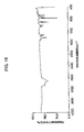
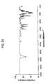
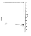
- FIGS. 2 and 3 are graphs showing IR and NMR spectra of compound I-1 in Example 1, respectively.
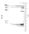
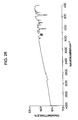
- FIGS. 4 and 5 are graphs showing IR and NMR spectra of compound II-1 in Example 2, respectively.
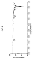
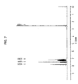
- FIGS. 6 and 7 are graphs showing IR and NMR spectra of compound VII-2 in Example 5, respectively.
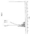
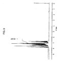
- FIGS. 8 and 9 are graphs showing IR and NMR spectra of compound VII-1 in Example 6, respectively.
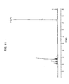
- FIGS. 10 and 11 are graphs showing IR and NMR spectra of compound VII-3 in Example 7, respectively.
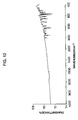
- FIGS. 12 and 13 are graphs showing IR and NMR spectra of compound VII-4 in Example 8, respectively.
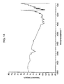
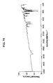
- FIGS. 14 and 15 are graphs showing IR and NMR spectra of compound VII-8 in Example 9, respectively.
- FIGS. 16 and 17 are graphs showing IR and NMR spectra of compound VII-12 in Example 10, respectively.
- FIGS. 18 and 19 are graphs showing IR and NMR spectra of compound VII-14 in Example 11, respectively.
- FIGS. 20 and 21 are graphs showing IR and NMR spectra of compound VII-15 in Example 12, respectively.
- FIGS. 22 and 23 are graphs showing IR and NMR spectra of compound VII-16 in Example 13, respectively.
- FIGS. 24 and 25 are graphs showing IR and NMR spectra of compound VII-24 in Example 14, respectively.
- FIGS. 26 and 27 are graphs showing IR and NMR spectra of compound VII-25 in Example 15, respectively.
- FIGS. 28 and 29 are graphs showing IR and NMR spectra of compound VII-26 in Example 16, respectively.
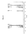
- FIGS. 30 and 31 are graphs showing IR and NMR spectra of compound I-20 in Example 17, respectively.
- FIGS. 32 and 33 are graphs showing IR and NMR spectra of compound VII-27 in Example 18, respectively.
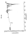
- FIGS. 34 and 35 are graphs showing IR and NMR spectra of compound VII-23 in Example 19, respectively.
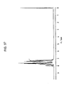
- FIGS. 36 and 37 are graphs showing IR and NMR spectra of compound I-17 in Example 20, respectively.
- novel phenylanthracene derivatives of the present invention are of formula (1).
- a 1 and A 2 each are a monophenylanthryl or diphenylanthryl group.
- a 1 and A 2 may be identical or different.
- the monophenylanthryl or diphenylanthryl group represented by A 1 and A 2 may be a substituted or unsubstituted one.
- exemplary substituents include alkyl, aryl, alkoxy, aryloxy, and amino groups, which may be further substituted. These substituents will be described later.
- the position of such substituents on the phenylanthryl group is not critical, the substituents are preferably positioned on the phenyl group bonded to the anthracene ring rather than on the anthracene ring.
- the phenyl group is bonded to the anthracene ring at its 9- and/or 10-position.
- L is a valence bond or a divalent linkage group.
- the preferred divalent linkage group is an arylene group which may have an intervening alkylene group, as will be described later.
- Preferred among the phenylanthracene derivatives of formula (1) are those of formulae (2) and (3).
- R 1 and R 2 are independently an alkyl, cycloalkyl, aryl, alkenyl, alkoxy, aryloxy, amino or heterocyclic group.
- the alkyl group represented by R 1 and R 2 may be a straight or branched, substituted or unsubstituted alkyl group, preferably having 1 to 10 carbon atoms, more preferably 1 to 4 carbon atoms. Especially preferred are unsubstituted alkyl groups having 1 to 4 carbon atoms, for example, methyl, ethyl, n- and i-propyl, and n-, i-, s- and t-butyl groups.
- Examples of the cycloalkyl group represented by R 1 and R 2 include cyclohexyl and cyclopentyl groups.
- the aryl group represented by R 1 and R 2 preferably has 6 to 20 carbon atoms and may have a substituent such as phenyl and tolyl.
- exemplary aryl groups are phenyl, o-, m-and p-tolyl, pyrenyl, naphthyl, anthryl, biphenyl, phenylanthryl, and tolylanthryl groups.
- the alkenyl group represented by R 1 and R 2 preferably has 6 to 50 carbon atoms in total and may be a substituted or unsubstituted one, preferably a substituted one wherein preferred substituents are aryl groups such as phenyl.
- Exemplary alkenyl groups are triphenylvinyl, tritolylvinyl and tribiphenylvinyl.
- the alkoxy group represented by R 1 and R 2 preferably has 1 to 6 carbon atoms in the alkyl moiety. Typical are methoxy and ethoxy groups.
- the alkoxy group may be a substituted one. Phenoxy is typical of the aryloxy group represented by R 1 and R 2 .
- the amino group represented by R 1 and R 2 may be a substituted or unsubstituted one, preferably substituted one.
- Exemplary substituents are alkyl groups such as methyl and ethyl and aryl groups such as phenyl.
- Examples of the amino group include diethylamino, diphenylamino, and di(m-tolyl)amino groups.
- Examples of the heterocyclic group represented by R 1 and R 2 include bipyridyl, pyrimidyl, quinolyl, pyridyl, thienyl, furyl, and oxadiazoyl groups. They may have a substituent such as methyl and phenyl.
- each of r1 and r2 is 0 or an integer of 1 to 5, preferably 0 or 1. Where each of r1 and r2 is an integer of 1 to 5, especially 1 or 2, each of R 1 and R 2 is preferably an alkyl, aryl, alkenyl, alkoxy, aryloxy or amino group.
- R 1 and R 2 may be identical or different. Where more than one group is included as R 1 (that is, r1 ⁇ 2), the R 1 groups may be identical or different or the R 1 groups, taken together, may form a ring such as a benzene ring. Likewise, where more than one group is included as R 2 (that is, r2 ⁇ 2), the R 2 groups may be identical or different or the R 2 groups, taken together, may form a ring such as a benzene ring. Those derivatives wherein the R 1 or R 2 groups form a ring are also preferred.
- L 1 is a valence bond or an arylene group.
- the arylene group represented by L 1 is preferably an unsubstituted one. Examples include ordinary arylene groups such as phenylene, biphenylene, and anthrylene while two or more directly bonded arylene groups are also included.
- L 1 is a valence bond, p-phenylene group, and 4,4'-biphenylene group.
- the arylene group represented by L 1 may be a group having two arylene groups separated by an alkylene group, -O-, -S- or -NR-.
- R is an alkyl or aryl group.
- Exemplary alkyl groups are methyl and ethyl and an exemplary aryl group is phenyl.
- R is an aryl group which is typically phenyl as just mentioned while it may be A 1 or A 2 or phenyl having A 1 or A 2 substituted thereon.
- Preferred alkylene groups are methylene and ethylene groups.
- R 3 and R 4 are as defined for R 1 and R 2 in formula (2), r3 and r4 are as defined for r1 and r2 in formula (2), and L 2 is as defined for L 1 in formula (2).
- Their preferred examples are also the same.
- R 3 and R 4 may be identical or different. Where more than one group is included as R 3 or R 4 , the R 3 groups may be identical or different as well as the R 4 groups. Alternatively, the R 3 or R 4 groups, taken together, may form a ring such as a benzene ring.
- the phenylanthracene derivatives according to the present invention can be prepared by coupling a halogenated diphenylanthracene compound with Ni(cod) 2 wherein cod represents 1,5-cyclooctadiene, or cross-coupling a Grignard reagent of a dihalogenated aryl with a nickel complex such as NiCl 2 (dppe) and NiCl 2 (dppp) wherein dppe represents diphenylphosphinoethane and dppp represents diphenylphosphinopropane.
- the phenylanthracene derivatives are prepared by a cross-coupling process involving reacting anthraquinone, benzoquinone, phenylanthrone or bianthrone with a Grignard reagent of aryl or a lithiated aryl followed by reduction.
- These compounds can be identified by elemental analysis, mass analysis, infrared absorption spectroscopy (IR), nuclear magnetic resonance spectroscopy ( 1 H and 13 C NMR), etc.
- the inventive compounds have a molecular weight of about 400 to about 2,000, preferably about 400 to about 1,000, a high melting point of about 200 to about 500°C, and a high glass transition temperature (Tg) of about 80 to about 250°C, preferably about 100 to 250°C, more preferably about 130 to 250°C, especially about 150 to 250°C.
- Tg glass transition temperature
- inventive vacuum deposition or the like they form a transparent, smooth film of quality which maintains a stable amorphous state even above room temperature and over a long period of time.
- the inventive compounds may be used alone or in admixture of two or more.
- the organic EL element of the invention includes at least one organic compound layer.
- the organic compound layer or at least one of organic compound layers contains the inventive compound.
- One exemplary structure of the organic EL element according to the present invention is shown in FIG. 1.
- the EL element generally designated at 1 in FIG. 1 includes on a substrate 2, an anode 3, a hole injecting and transporting layer 4, a light emitting layer 5, an electron injecting and transporting layer 6, and a cathode 7 stacked in the described order from bottom to top.
- the light emitting layer has multi-functions of injecting holes and electrons, transporting them, and recombining holes and electrons to create excitons.
- the hole injecting and transporting layer has functions of facilitating injection of holes from the anode, transporting them, and obstructing electron transportation.
- the electron injecting and transporting layer has functions of facilitating injection of electrons from the cathode, transporting them, and obstructing hole transportation.
- the hole and electron injecting and transporting layers are optionally provided by taking into account the magnitude of the respective functions of the compound used in the light emitting layer for electron injection and transportation and hole injection and transportation.
- the hole or electron injecting and transporting layer may be omitted because the light emitting layer itself can also serve as a hole or electron injecting and transporting layer.
- both the hole and electron injecting and transporting layers may be omitted.
- Each of the hole and electron injecting and transporting layers may consist of two sublayers, one sublayer having an injecting function and another sublayer having a transporting function.
- the inventive compound is preferably used in a light emitting layer because it is relatively neutral although it is also applicable to either a hole injecting and transporting layer or an electron injecting and transporting layer.
- a freedom of design of the recombination/light emitting region is available by controlling the film thickness in consideration of the carrier mobility and carrier density (which is dependent on ionization potential and electron affinity) of the light emitting layer, hole injecting and transporting layer, and electron injecting and transporting layer to be combined. This enables free design of luminous color, control of the luminance and spectrum of light emission by the interference of the electrodes, and control of the space distribution of light emission.
- the light emitting layer may additionally contain another luminescent material.
- the luminescent material may be selected from compounds as disclosed in JP-A 264692/1988, for example, quinacridone, rubrene, and styryl series dyes alone or in admixture. Such a luminescent material is preferably contained in the light emitting layer in an amount of less than 10 mol% of the inventive compound. By adding a selected luminescent material, the light emitted by the layer can be shifted to a longer wavelength side.
- the light emitting layer may further contain a singlet oxygen quencher.
- exemplary quenchers include nickel complexes, rubrene, diphenylisobenzofuran, and tertiary amines. Such a quencher is preferably present in an amount of less than 10 mol% of the inventive compound.
- any of various organic compounds used in conventional organic EL elements for example, the organic compounds described in JP-A 295695/1988, 191694/1990, and 000792/1991 may be used in the hole injecting and transporting layer and electron injecting and transporting layer.
- any of aromatic tertiary amines, hydrazone derivatives, carbazole derivatives, triazole derivatives, and imidazole derivatives may be used.
- organic metal complex derivatives such as aluminum quinolinol, oxadiazole derivatives, pyridine derivatives, pyrimidine derivatives, quinoline derivatives, quinoxaline derivatives, diphenylquinone derivatives, perylene derivatives, and fluorene derivatives may be used.
- the hole injecting and transporting layer is formed as comprising a hole injecting layer and a hole transporting layer
- two or more compounds are selected in a proper combination from the compounds commonly used in hole injecting and transporting layers.
- laminate layers such that a layer of a compound having a lower ionization potential may be disposed adjacent to the anode (ITO etc.).
- ITO etc. anode
- a compound having good thin film forming ability at the anode surface is also preferred.
- This order of lamination also applies where a plurality of hole injecting and transporting layers are provided. Such an order of lamination is effective for lowering drive voltage and preventing current leakage and development and growth of local dark spots.
- thin films of about 1 to 10 nm thick can be formed uniform and pinhole-free, which restrains any change in color tone of light emission and a drop of efficiency by re-absorption even if a compound having a low ionization potential and absorption in the visible range is used in the hole injecting layer.
- the electron injecting and transporting layer is formed as comprising an electron injecting layer and an electron transporting layer
- two or more compounds are selected in a proper combination from the compounds commonly used in electron injecting and transporting layers.
- the light emitting layer be a mix layer containing a mixture of a hole injecting and transporting compound and an electron injecting and transporting compound.
- the inventive compound is contained in the mix layer. Since the inventive compound is generally contained as a fluorescent material, in one embodiment wherein the inventive compound is an electron injecting and transporting compound, it is preferred to further add a hole injecting and transporting compound. In another embodiment wherein the inventive compound is a hole injecting and transporting compound, it is preferred to further add an electron injecting and transporting compound.
- the electron injecting and transporting compound and hole injecting and transporting compound are preferably mixed such that the weight ratio of electron injecting and transporting compound to hole injecting and transporting compound may range from 60:40 to 40:60, especially about 50:50.
- an electron injecting and transporting compound may be selected from the above-mentioned electron injecting and transporting compounds and a hole injecting and transporting compound may be selected from the above-mentioned hole injecting and transporting compounds. If desired, any of the inventive compounds may be selected.
- each of the electron injecting and transporting compound and hole injecting and transporting compound may be used alone or in admixture of two or more.
- the mix layer may be doped with the inventive compound or another fluorescent material for enhancing luminous intensity.
- a mix layer of an electron injecting and transporting compound and a hole injecting and transporting compound both other than the above-mentioned ones may be doped with the inventive compound.
- an EL element is improved in stability.
- the fluorescent material used in the light emitting layer may be selected from those capable of fluorescence at an equal or longer wavelength as compared with the inventive compound, for example, from those fluorescent materials which can be used in combination with the inventive compound in the light emitting layer.
- the inventive compound may be further used in the light emitting layer.
- the inventive compound may be further used in the light emitting layer which also serves as an electron injecting and transporting layer.
- the fluorescent material used in the light emitting layer may be selected from those capable of fluorescence at a longer wavelength as compared with the inventive compound, for example, from those fluorescent materials which can be used in combination with the inventive compound in the light emitting layer.
- the inventive compound may be further used in the light emitting layer.
- the inventive compound may be added and combined as an additional fluorescent material in an amount of less than 10 mol%.
- the thicknesses of the light emitting layer, hole injecting and transporting layer, and electron injecting and transporting layer are not critical and varies with a particular formation technique. Usually a single layer is 5 to 1,000 nm thick, especially 8 to 200 nm thick.
- the thicknesses of the hole injecting and transporting layer and electron injecting and transporting layer are equal to or range from 1/10 to 10 times the thickness of the light emitting layer although they depend on the design of a recombination/light emitting region.
- the electron or hole injecting and transporting layer is divided into an injecting layer and a transporting layer, preferably the injecting layer is at least 1 nm thick and the transporting layer is at least 20 nm thick.
- the upper limit of thickness is about 100 nm for the injecting layer and about 1,000 nm for the transporting layer.
- the cathode is preferably made of a material having a low work function, for example, Li, Na, Mg, Al, Ag, In and alloys containing at least one of these metals.
- the cathode should preferably be of fine grains, especially amorphous.
- the cathode is preferably 10 to 1,000 nm thick.
- the EL element In order that the EL element produce plane light emission, at least one of the electrodes should be transparent or translucent. Since the material of the cathode is limited as mentioned just above, it is preferred to select the material and thickness of the anode so as to provide a transmittance of at least 80% to the emitted radiation.
- the anode is preferably made of indium tin oxide (ITO), SnO 2 , Ni, Au, Pt, Pd, and doped polypyrrole.
- the anode preferably has a thickness of about 10 to 500 nm.
- the drive voltage should be low. To this end, ITO having 10 to 30 ⁇ /cm 2 or less than 10 ⁇ /cm 2 (commonly 5 to 10 ⁇ /cm 2 ) is preferred, for example.
- the substrate may be made of any desired material although a transparent or translucent material such as glass and resins is used in the illustrated embodiment wherein light exits from the substrate side.
- the substrate may be provided with a color filter layer or dielectric reflecting film for controlling emission light color. Where the substrate is made of an opaque material, the layer stacking order may be reversed from that shown in FIG. 1.
- the cathode and anode are preferably formed by gas phase deposition techniques such as vacuum evaporation and sputtering.
- the light emitting layer and hole and electron injecting and transporting layers are preferably formed by vacuum evaporation because homogeneous thin films are available.
- vacuum evaporation By utilizing vacuum evaporation, there is obtained a homogeneous thin film which is amorphous or has a grain size of less than 0.1 ⁇ m and typically upward of 0.01 ⁇ m. If the grain size is more than 0.1 ⁇ m, uneven light emission takes place and the drive voltage of the element must be increased with a substantial lowering of electric charge injection efficiency.
- the conditions for vacuum evaporation are not critical although a vacuum of 1 ⁇ 3 x 10 -3 N/m 2 (10 -5 Torr) or lower and an evaporation rate of 0.1 to 1 nm/sec. are preferred. It is preferred to successively form layers in vacuum because the successive formation in vacuum can avoid adsorption of impurities at the interface between the layers, thus ensuring higher quality and a lower drive voltage.
- boats having the compounds received therein are individually temperature controlled to achieve co-deposition while monitoring the film thickness by means of a quartz oscillator film thickness gage.
- the EL element of the invention is generally of the DC drive type while it can be of the AC or pulse drive type.
- the applied voltage is generally 2 to 20 volts.
- DSC differential scanning calorimetry
- mp is a melting point
- Tg is a glass transition temperature
- THF is tetrahydrofuran.
- reaction solution was poured into 1m (1N) aqueous hydrochloric acid, from which the product was extracted with toluene and chloroform, washed with water and then dried over magnesium sulfate.
- the product was precipitated from acetone again, recrystallized three times from chloroform, and purified through a silica column using toluene as the extracting solvent, yielding 0.53 g of a yellowish white solid. This yellowish white solid, 0.5 g, was purified through sublimation, yielding 0.23 g of a yellowish white solid having blue fluorescence. Elemental analysis C H Calcd. (%) 94.80 5.20 Found (%) 94.96 4.90
- reaction solution was poured into 1m (1N) aqueous hydrochloric acid, from which the product was extracted with toluene and chloroform, washed with water and then dried over magnesium sulfate. After the solvent was distilled off, the product was recrystallized from acetone/dichloromethane and purified through a silica column using toluene and hexanol as the extracting solvent, yielding 2.0 g of a yellowish white solid having blue-green fluorescence. This yellowish white solid, 1.0 g, was purified through sublimation, yielding 0.6 g of a pure yellowish white solid.
- the reaction solution was poured into 1m (1N) aqueous hydrochloric acid, from which the product was extracted with toluene and chloroform, washed with water and then dried over magnesium sulfate.
- the product was dissolved in 100 ml of acetic acid, to which an aqueous solution of hydrogen iodide was added dropwise. The solution was stirred for 4 hours.
- a hydrochloric acid solution of tin dichloride (SnCl 2 ) was added to the solution until the liberated iodine disappeared.
- the product was extracted with chloroform and toluene and dried over magnesium sulfate. After the solvent was distilled off, the product was purified through a silica column using toluene as the extracting solvent and recrystallized from acetone/toluene.
- a glass substrate having an ITO transparent electrode (anode) of 100 nm thick was subjected to ultrasonic cleaning with neutral detergent, acetone, and ethanol, pulled up from boiling ethanol, and dried.
- the substrate was secured by a holder in an evaporation chamber, which was evacuated to a vacuum of 1 ⁇ 3 x 10 -4 N/m 2 (1x10 -6 Torr).
- N,N'-diphenyl-N,N'-m-tolyl-4,4'-diamino-1,1'-biphenyl (designated TPD-1) was evaporated at a deposition rate of 0.2 nm/sec. to a thickness of 50 nm, forming a hole injecting and transporting layer.
- compound I-1 of Example 1 was evaporated at a deposition rate of 0.2 nm/sec. to a thickness of 50 nm, forming a light emitting layer.
- tris(8-quinolinolato)aluminum was evaporated at a deposition rate of 0.2 nm/sec. to a thickness of 10 nm, forming an electron injecting and transporting layer.
- MgAg weight ratio 10:1
- a glass substrate having an ITO transparent electrode (anode) of 100 nm thick was subjected to ultrasonic cleaning with neutral detergent, acetone, and ethanol, pulled up from boiling ethanol, and dried.
- the substrate was secured by a holder in an evaporation chamber, which was evacuated to a vacuum of 1 ⁇ 3 x 10 -4 N/m 2 (1x10 -6 Torr).
- poly(thiophene-2,5-diyl) was evaporated to a thickness of 10 nm, forming a hole injecting layer.
- N,N'-diphenyl-N,N'-m-tolyl-4,4'-diamino-1,1'-biphenyl (TPD-1) was evaporated at a deposition rate of 0.2 nm/sec. to a thickness of 50 nm, forming a hole transporting layer.
- tris(8-quinolinolato)aluminum was evaporated at a deposition rate of 0.2 nm/sec. to a thickness of 10 nm, forming an electron injecting and transporting layer.
- MgAg weight ratio 10:1
- An EL element was fabricated by the same procedure as in Example 22 except that the electron injecting and transporting layer was omitted.
- An EL element was fabricated by the same procedure as in Example 22 except that the hole transporting material TPD-1 was replaced by N,N,N',N'-tetrakis(3-biphenyl)-4,4'-diamino-1,1'-biphenyl (designated TPD-2).
- a hole transporting layer was formed as in Example 24 before a light emitting layer was formed by co-evaporating TPD-2 and compound I-1 of Example 1 in a weight ratio of 1:1 at a deposition rate of 0.2 nm/sec. to a thickness of 20 nm.
- compound I-1 of Example 1 was evaporated to a thickness of 50 nm, forming an electron transporting layer.
- tris(8-quinolinolato)aluminum was evaporated at a deposition rate of 0.2 nm/sec. to a thickness of 10 nm, forming an electron injecting layer.
- MgAg weight ratio 10:1
- a glass substrate having an ITO transparent electrode (anode) of 100 nm thick was subjected to ultrasonic cleaning with neutral detergent, acetone, and ethanol, pulled up from boiling ethanol, and dried.
- the substrate was secured by a holder in an evaporation chamber, which was evacuated to a vacuum of 1 ⁇ 6 x 10 -4 N/m 2 (1x10 -6 Torr).
- poly(thiophene-2,5-diyl) was evaporated to a thickness of 10 nm, forming a hole injecting layer.
- N,N'-diphenyl-N,N'-m-tolyl-4,4'-diamino-1,1'-biphenyl (TPD-1) was evaporated at a deposition rate of 0.2 nm/sec. to a thickness of 50 nm, forming a hole transporting layer.
- tris(8-quinolinolato)aluminum was evaporated at a deposition rate of 0.2 nm/sec. to a thickness of 10 nm, forming an electron injecting and transporting layer.
- MgAg weight ratio 10:1
- An EL element was fabricated by the same procedure as in Example 21 except that compound VII-2 of Example 5 was used instead of compound I-1.
- An EL element was fabricated by the same procedure as in Example 22 except that after formation of the light emitting layer, tris(8-quinolinolato)aluminum was evaporated at a deposition rate of 0.2 nm/sec. to a thickness of 20 nm to form an electron transporting layer and thereafter, tetrabutyldiphenoquinone was evaporated to a thickness of 10 nm to form an electron injecting layer.
- a glass substrate having an ITO transparent electrode (anode) of 100 nm thick was subjected to ultrasonic cleaning with neutral detergent, acetone, and ethanol, pulled up from boiling ethanol, and dried.
- the substrate was secured by a holder in an evaporation chamber, which was evacuated to a vacuum of 1 ⁇ 3 x 10 -4 N/m 2 (1x10 -6 Torr).
- poly(thiophene-2,5-diyl) was evaporated to a thickness of 10 nm, forming a hole injecting layer.
- N,N'-diphenyl-N,N'-m-tolyl-4,4'-diamino-1,1'-biphenyl (TPD-1) was evaporated at a deposition rate of 0.2 nm/sec. to a thickness of 50 nm, forming a hole transporting layer.
- tetraphenylcyclopentadiene was evaporated to a thickness of 50 nm to form a light emitting layer.
- compound I-1 of Example 1 was evaporated at a deposition rate of 0.2 nm/sec. to a thickness of 10 nm, forming an electron injecting and transporting layer.
- MgAg weight ratio 10:1
- Additional organic EL elements were fabricated in accordance with Examples 21 to 29 by appropriately selecting one or more compounds from the inventive compounds of formulae (I) to (X) and using them as the light emitting layer or the electron injecting and transporting layer in appropriate combinations other than the above-mentioned combinations. Equivalent results were obtained in accordance with the layer structure of the respective EL elements.
- a glass substrate having an ITO transparent electrode (anode) of 100 nm thick was subjected to ultrasonic cleaning with neutral detergent, acetone, and ethanol, pulled up from boiling ethanol, and dried.
- the substrate was secured by a holder in an evaporation chamber, which was evacuated to a vacuum of 1 ⁇ 3 x 10 -4 N/m 2 (1x10 -6 Torr).
- N,N'-diphenyl-N,N'-m-tolyl-4,4'-diamino-1,1'-biphenyl (TPD-1) was evaporated to a thickness of 50 nm, forming a hole injecting and transporting layer.
- 1,3-bis(5-(4-t-butylphenyl)-1,3,4-oxadiazo-2-yl)benzene (designated OXD-7) was evaporated at a deposition rate of 0.2 nm/sec. to a thickness of 50 nm, forming a light emitting layer.
- tris(8-quinolinolato)aluminum was evaporated at a deposition rate of 0.2 nm/sec. to a thickness of 10 nm, forming an electron injecting and transporting layer.
- MgAg weight ratio 10:1
- An organic EL element was fabricated in accordance with C. Adachi et al., Applied Phys. Lett., 56, 799 (1990) using 9,10-diphenylanthracene described therein as a light emitting layer. More specifically, in Comparative Example 1, the electron injecting and transporting layer was omitted and instead, 9,10-diphenylanthracene was evaporated to a thickness of 50 nm to form a light emitting layer also serving as an electron injecting and transporting layer.
- the organic compound layer was crystalline.
- emission of blue light was observed, but dielectric breakdown occurred shortly.
- phenylanthracene derivatives which are effective for forming good thin films in a less crystalline or amorphous state. They can be used as compounds for organic EL elements, especially as blue light emitting material and electron injecting and transporting material.
- organic EL elements using phenylanthracene derivatives according to the present invention are free of current leakage and eliminate development and growth of dark spots. These, combined with restrained crystallization in the film of phenylanthracene derivative, result in a reliable element capable of continuous light emission. Particularly when used in the light emitting layer, the phenylanthracene derivatives ensure emission of blue light at a high luminance of 10,000 cd/m 2 or more.
Description
- This invention generally relates to an organic electroluminescent (EL) element and more particularly, to an organic EL element of the type wherein an electric field is applied across an organic compound layer in a multilayer structure to emit light.
- Organic electroluminescent (EL) elements include a thin film containing a luminescent organic compound interleaved between a cathode and an anode. Electrons and holes are injected into the thin film where they are recombined to create excitons. Light is emitted by utilizing luminescence (phosphorescence or fluorescence) upon deactivation of excitons. The organic EL elements are characterized by plane light emission at a high luminance of about 100 to 100,000 cd/m2 with a low voltage of about 10 volts and light emission in a spectrum from blue to red color by a simple choice of the type of fluorescent material.
- The organic EL elements, however, are undesirably short in effective life, less durable during storage and less reliable because of the following factors.
- (1) Physical changes of organic compounds: Growth of crystal grain domains renders the interface non-uniform, which causes deterioration of electric charge injecting ability, short-circuiting and dielectric breakdown of the element. Particularly when a low molecular weight compound having a molecular weight of less than 500 is used, grains develop and grow, substantially detracting from film quality. Even when the interface with indium tin oxide (ITO) is rough, significant development and growth of grains occur to lower luminous efficiency and allow current leakage, ceasing to emit light. Local dark spots are also formed.
- (2) Oxidation and stripping of the cathode: Although metals having a low work function such as Na, Mg, and Al are used as the cathode in order to facilitate electron injection, these metals are reactive with oxygen and moisture in air. As a result, the cathode can be stripped from the organic compound layer, prohibiting electric charge injection. Particularly when a polymeric compound is applied as by spin coating, the residual solvent and decomposed products resulting from film formation promote oxidation reaction of the electrodes which can be stripped to create local dark spots.
- (3) Low luminous efficiency and increased heat build-up: Since electric current is conducted across an organic compound, the organic compound is placed under an electric field of high strength and cannot help heating. The heat causes melting, crystallization or decomposition of the organic compound, leading to deterioration or failure of the element.
- (4) Photo-chemical and electro-chemical changes of organic compound layers.
-
- With respect to blue light-emitting devices, in particular, there are available few blue light-emitting substances which can provide for reliable stable devices. In general, blue light-emitting substances are highly crystalline. For example, diphenylanthracene has high crystallinity despite a high fluorescent quantum yield. Using this compound as a light emitting material fails to manufacture a reliable device having high luminance and high efficiency. See C. Adachi et al., Applied Phys. Lett., 56, 799 (1990).
- Therefore, an object of the present invention is to provide a phenylanthracene derivative which is novel as an opto-electronic functional material and experiences minimal physical changes, photo-chemical changes and electrochemical changes.
- Another object of the present invention is to provide a novel and improved organic EL element using the phenyl-anthracene derivative, the element featuring high reliability, high luminous efficiency and an ability to emit a wide spectrum of light, especially blue light.
- A further object of the present invention is to provide a high reliability, high luminance light emitting element having an organic thin film formed by evaporation of a high molecular weight compound, the element featuring minimized voltage rise, luminance drop, current leakage, and development or growth of local dark spots during operation of the element.
- In a first aspect, the present invention provides a phenylanthracene derivative of the following general formula (1):
- In one preferred embodiment, the phenylanthracene derivative is of the following formula (2):wherein each of R1 and R2, which may be identical or different, is selected from the group consisting of an alkyl, cycloalkyl, aryl, alkenyl, alkoxy, aryloxy, amino and heterocyclic group, each of r1 and r2 is 0 or an integer of 1 to 5, and L1 is a valence bond or an arylene group which may have an intervening group in the form of an alkylene group, -O-, -S- or -NR- wherein R is an alkyl or aryl group. Where r1 is an integer of 2 to 5, the R1 groups may be identical or different or the R1 groups, taken together, may form a ring. Similarly, where r2 is an integer of 2 to 5, the R2 groups may be identical or different or the R2 groups, taken together, may form a ring.

- In one preferred embodiment, the phenylanthracene derivative is of the following formula (3):wherein each of R3 and R4, which may be identical or different, is selected from the group consisting of an alkyl, cycloalkyl, aryl, alkenyl, alkoxy, aryloxy, amino and heterocyclic group, each of r3 and r4 is 0 or an integer of 1 to 5, and L2 is a valence bond or an arylene group which may have an intervening group in the form of an alkylene group, -O-, -S- or -NR- wherein R is an alkyl or aryl group. Where r3 is an integer of 2 to 5, the R3 groups may be identical or different or the R3 groups, taken together, may form a ring. Where r4 is an integer of 2 to 5, the R4 groups may be identical or different or the R4 groups, taken together, may form a ring.

- In a second aspect, the present invention provides an organic electroluminescent (EL) element comprising at least one organic compound layer containing the phenylanthracene derivative defined above.
- In one preferred embodiment, the organic compound layer containing the phenylanthracene derivative is a light emitting layer. The organic EL element may further include at least one hole injecting layer, at least one hole transporting layer, and at least one electron injecting and transporting layer. Alternatively, the organic EL element may further include at least one hole injecting layer, at least one hole transporting layer, at least one electron transporting layer, and at least one electron injecting layer.
- In another preferred embodiment, the organic compound layer containing the phenylanthracene derivative is an electron injecting and transporting layer. In this case, the element further includes a light emitting layer.
- In a further preferred embodiment, the organic EL element includes at least one light emitting layer which is a mix layer formed of a mixture of an electron injecting and transporting compound and a hole injecting and transporting compound. The phenylanthracene derivative is contained in the mix layer.
- Where an inventive compound of formula (1), preferably formula (2) or (3) is used in a light emitting layer, the organic EL element of the present invention can emit light at a luminance as high as 10,000 cd/m2 or more in a stable manner. The element ensures stable driving with a current density of about 1,000 mA/cm2. The element is resistant to heat and durable.
- The inventive compound can be evaporated to deposit thin films in a stable amorphous state. Owing to good physical properties, the thin films are capable of uniformly emitting light. In the ambient air they remain stable over one year without crystallization. The compound can also be spin coated from a chloroform solution, forming stable amorphous thin films.
- The organic EL element is capable of efficient light emission with a low driving voltage. Note that the element emits light with a maximum wavelength of 400 nm to 700 nm.
- The foregoing aspects and other features of the invention are explained in the following description, taken in connection with the accompanying drawings.
- FIG. 1 is a side elevation of an exemplary organic EL element according to one embodiment of the invention.
- FIGS. 2 and 3 are graphs showing IR and NMR spectra of compound I-1 in Example 1, respectively.
- FIGS. 4 and 5 are graphs showing IR and NMR spectra of compound II-1 in Example 2, respectively.
- FIGS. 6 and 7 are graphs showing IR and NMR spectra of compound VII-2 in Example 5, respectively.
- FIGS. 8 and 9 are graphs showing IR and NMR spectra of compound VII-1 in Example 6, respectively.
- FIGS. 10 and 11 are graphs showing IR and NMR spectra of compound VII-3 in Example 7, respectively.
- FIGS. 12 and 13 are graphs showing IR and NMR spectra of compound VII-4 in Example 8, respectively.
- FIGS. 14 and 15 are graphs showing IR and NMR spectra of compound VII-8 in Example 9, respectively.
- FIGS. 16 and 17 are graphs showing IR and NMR spectra of compound VII-12 in Example 10, respectively.
- FIGS. 18 and 19 are graphs showing IR and NMR spectra of compound VII-14 in Example 11, respectively.
- FIGS. 20 and 21 are graphs showing IR and NMR spectra of compound VII-15 in Example 12, respectively.
- FIGS. 22 and 23 are graphs showing IR and NMR spectra of compound VII-16 in Example 13, respectively.
- FIGS. 24 and 25 are graphs showing IR and NMR spectra of compound VII-24 in Example 14, respectively.
- FIGS. 26 and 27 are graphs showing IR and NMR spectra of compound VII-25 in Example 15, respectively.
- FIGS. 28 and 29 are graphs showing IR and NMR spectra of compound VII-26 in Example 16, respectively.
- FIGS. 30 and 31 are graphs showing IR and NMR spectra of compound I-20 in Example 17, respectively.
- FIGS. 32 and 33 are graphs showing IR and NMR spectra of compound VII-27 in Example 18, respectively.
- FIGS. 34 and 35 are graphs showing IR and NMR spectra of compound VII-23 in Example 19, respectively.
- FIGS. 36 and 37 are graphs showing IR and NMR spectra of compound I-17 in Example 20, respectively.
- The novel phenylanthracene derivatives of the present invention are of formula (1).
- A1 and A2 each are a monophenylanthryl or diphenylanthryl group. A1 and A2 may be identical or different. The monophenylanthryl or diphenylanthryl group represented by A1 and A2 may be a substituted or unsubstituted one. Where substituted, exemplary substituents include alkyl, aryl, alkoxy, aryloxy, and amino groups, which may be further substituted. These substituents will be described later. Although the position of such substituents on the phenylanthryl group is not critical, the substituents are preferably positioned on the phenyl group bonded to the anthracene ring rather than on the anthracene ring. Preferably the phenyl group is bonded to the anthracene ring at its 9- and/or 10-position.
- In formula (1), L is a valence bond or a divalent linkage group. The preferred divalent linkage group is an arylene group which may have an intervening alkylene group, as will be described later.
- Preferred among the phenylanthracene derivatives of formula (1) are those of formulae (2) and (3).
- First, formula (2) is described.

- R1 and R2 are independently an alkyl, cycloalkyl, aryl, alkenyl, alkoxy, aryloxy, amino or heterocyclic group.
- The alkyl group represented by R1 and R2 may be a straight or branched, substituted or unsubstituted alkyl group, preferably having 1 to 10 carbon atoms, more preferably 1 to 4 carbon atoms. Especially preferred are unsubstituted alkyl groups having 1 to 4 carbon atoms, for example, methyl, ethyl, n- and i-propyl, and n-, i-, s- and t-butyl groups. Examples of the cycloalkyl group represented by R1 and R2 include cyclohexyl and cyclopentyl groups. The aryl group represented by R1 and R2 preferably has 6 to 20 carbon atoms and may have a substituent such as phenyl and tolyl. Exemplary aryl groups are phenyl, o-, m-and p-tolyl, pyrenyl, naphthyl, anthryl, biphenyl, phenylanthryl, and tolylanthryl groups. The alkenyl group represented by R1 and R2 preferably has 6 to 50 carbon atoms in total and may be a substituted or unsubstituted one, preferably a substituted one wherein preferred substituents are aryl groups such as phenyl. Exemplary alkenyl groups are triphenylvinyl, tritolylvinyl and tribiphenylvinyl. The alkoxy group represented by R1 and R2 preferably has 1 to 6 carbon atoms in the alkyl moiety. Typical are methoxy and ethoxy groups. The alkoxy group may be a substituted one. Phenoxy is typical of the aryloxy group represented by R1 and R2. The amino group represented by R1 and R2 may be a substituted or unsubstituted one, preferably substituted one. Exemplary substituents are alkyl groups such as methyl and ethyl and aryl groups such as phenyl. Examples of the amino group include diethylamino, diphenylamino, and di(m-tolyl)amino groups. Examples of the heterocyclic group represented by R1 and R2 include bipyridyl, pyrimidyl, quinolyl, pyridyl, thienyl, furyl, and oxadiazoyl groups. They may have a substituent such as methyl and phenyl.
- In formula (2), each of r1 and r2 is 0 or an integer of 1 to 5, preferably 0 or 1. Where each of r1 and r2 is an integer of 1 to 5, especially 1 or 2, each of R1 and R2 is preferably an alkyl, aryl, alkenyl, alkoxy, aryloxy or amino group.
- R1 and R2 may be identical or different. Where more than one group is included as R1 (that is, r1 ≥ 2), the R1 groups may be identical or different or the R1 groups, taken together, may form a ring such as a benzene ring. Likewise, where more than one group is included as R2 (that is, r2 ≥ 2), the R2 groups may be identical or different or the R2 groups, taken together, may form a ring such as a benzene ring. Those derivatives wherein the R1 or R2 groups form a ring are also preferred.
- L1 is a valence bond or an arylene group. The arylene group represented by L1 is preferably an unsubstituted one. Examples include ordinary arylene groups such as phenylene, biphenylene, and anthrylene while two or more directly bonded arylene groups are also included. Preferably L1 is a valence bond, p-phenylene group, and 4,4'-biphenylene group.
- The arylene group represented by L1 may be a group having two arylene groups separated by an alkylene group, -O-, -S- or -NR-. R is an alkyl or aryl group. Exemplary alkyl groups are methyl and ethyl and an exemplary aryl group is phenyl. Preferably R is an aryl group which is typically phenyl as just mentioned while it may be A1 or A2 or phenyl having A1 or A2 substituted thereon. Preferred alkylene groups are methylene and ethylene groups.
- Examples of the arylene group represented by L1 are shown below.


- Next, formula (3) is described.

- In formula (3), R3 and R4 are as defined for R1 and R2 in formula (2), r3 and r4 are as defined for r1 and r2 in formula (2), and L2 is as defined for L1 in formula (2). Their preferred examples are also the same.
- Also in formula (3), R3 and R4 may be identical or different. Where more than one group is included as R3 or R4, the R3 groups may be identical or different as well as the R4 groups. Alternatively, the R3 or R4 groups, taken together, may form a ring such as a benzene ring.
- Illustrative, non-limiting examples of the compounds formulae (2) and (3) are shown below. Examples are represented by general formulae (I) to (VII) wherein substituents R11 to R15, R21 to R25, R31 to R35, and R41 to R45 have the meaning and combination shown in Tables 1 to 7, respectively. Formulae (VIII), (IX), and (X) show specific structures.


- The phenylanthracene derivatives according to the present invention, which are sometimes referred to as inventive compounds, can be prepared by coupling a halogenated diphenylanthracene compound with Ni(cod)2 wherein cod represents 1,5-cyclooctadiene, or cross-coupling a Grignard reagent of a dihalogenated aryl with a nickel complex such as NiCl2(dppe) and NiCl2(dppp) wherein dppe represents diphenylphosphinoethane and dppp represents diphenylphosphinopropane. Alternatively, the phenylanthracene derivatives are prepared by a cross-coupling process involving reacting anthraquinone, benzoquinone, phenylanthrone or bianthrone with a Grignard reagent of aryl or a lithiated aryl followed by reduction. These compounds can be identified by elemental analysis, mass analysis, infrared absorption spectroscopy (IR), nuclear magnetic resonance spectroscopy (1H and 13C NMR), etc.
- In general, the inventive compounds have a molecular weight of about 400 to about 2,000, preferably about 400 to about 1,000, a high melting point of about 200 to about 500°C, and a high glass transition temperature (Tg) of about 80 to about 250°C, preferably about 100 to 250°C, more preferably about 130 to 250°C, especially about 150 to 250°C. By conventional vacuum deposition or the like, they form a transparent, smooth film of quality which maintains a stable amorphous state even above room temperature and over a long period of time. The inventive compounds may be used alone or in admixture of two or more.
- The organic EL element of the invention includes at least one organic compound layer. The organic compound layer or at least one of organic compound layers contains the inventive compound. One exemplary structure of the organic EL element according to the present invention is shown in FIG. 1. The EL element generally designated at 1 in FIG. 1 includes on a
substrate 2, ananode 3, a hole injecting and transportinglayer 4, alight emitting layer 5, an electron injecting and transportinglayer 6, and acathode 7 stacked in the described order from bottom to top. - The light emitting layer has multi-functions of injecting holes and electrons, transporting them, and recombining holes and electrons to create excitons. The hole injecting and transporting layer has functions of facilitating injection of holes from the anode, transporting them, and obstructing electron transportation. The electron injecting and transporting layer has functions of facilitating injection of electrons from the cathode, transporting them, and obstructing hole transportation. These two layers are effective for increasing the number of holes and electrons injected into the light emitting layer and confining holes and electrons therein for optimizing the recombination region to improve light emission efficiency. Therefore the hole and electron injecting and transporting layers are optionally provided by taking into account the magnitude of the respective functions of the compound used in the light emitting layer for electron injection and transportation and hole injection and transportation. For example, if the compound used in the light emitting layer has an enhanced hole or electron injecting and transporting function, the hole or electron injecting and transporting layer may be omitted because the light emitting layer itself can also serve as a hole or electron injecting and transporting layer. In some cases, both the hole and electron injecting and transporting layers may be omitted. Each of the hole and electron injecting and transporting layers may consist of two sublayers, one sublayer having an injecting function and another sublayer having a transporting function.
- The inventive compound is preferably used in a light emitting layer because it is relatively neutral although it is also applicable to either a hole injecting and transporting layer or an electron injecting and transporting layer.
- A freedom of design of the recombination/light emitting region is available by controlling the film thickness in consideration of the carrier mobility and carrier density (which is dependent on ionization potential and electron affinity) of the light emitting layer, hole injecting and transporting layer, and electron injecting and transporting layer to be combined. This enables free design of luminous color, control of the luminance and spectrum of light emission by the interference of the electrodes, and control of the space distribution of light emission.
- Described below is the embodiment wherein the inventive compounds are used in the light emitting layer. The light emitting layer may additionally contain another luminescent material. The luminescent material may be selected from compounds as disclosed in JP-A 264692/1988, for example, quinacridone, rubrene, and styryl series dyes alone or in admixture. Such a luminescent material is preferably contained in the light emitting layer in an amount of less than 10 mol% of the inventive compound. By adding a selected luminescent material, the light emitted by the layer can be shifted to a longer wavelength side.
- The light emitting layer may further contain a singlet oxygen quencher. Exemplary quenchers include nickel complexes, rubrene, diphenylisobenzofuran, and tertiary amines. Such a quencher is preferably present in an amount of less than 10 mol% of the inventive compound.
- In the preferred embodiment wherein the inventive compounds are used in the light emitting layer, any of various organic compounds used in conventional organic EL elements, for example, the organic compounds described in JP-A 295695/1988, 191694/1990, and 000792/1991 may be used in the hole injecting and transporting layer and electron injecting and transporting layer. For example, in the hole injecting and transporting layer, any of aromatic tertiary amines, hydrazone derivatives, carbazole derivatives, triazole derivatives, and imidazole derivatives may be used. For the electron injecting and transporting layer, organic metal complex derivatives such as aluminum quinolinol, oxadiazole derivatives, pyridine derivatives, pyrimidine derivatives, quinoline derivatives, quinoxaline derivatives, diphenylquinone derivatives, perylene derivatives, and fluorene derivatives may be used.
- Where the hole injecting and transporting layer is formed as comprising a hole injecting layer and a hole transporting layer, two or more compounds are selected in a proper combination from the compounds commonly used in hole injecting and transporting layers. In this regard, it is preferred to laminate layers such that a layer of a compound having a lower ionization potential may be disposed adjacent to the anode (ITO etc.). It is also preferred to use a compound having good thin film forming ability at the anode surface. This order of lamination also applies where a plurality of hole injecting and transporting layers are provided. Such an order of lamination is effective for lowering drive voltage and preventing current leakage and development and growth of local dark spots. Since evaporation is utilized in manufacturing elements, thin films of about 1 to 10 nm thick can be formed uniform and pinhole-free, which restrains any change in color tone of light emission and a drop of efficiency by re-absorption even if a compound having a low ionization potential and absorption in the visible range is used in the hole injecting layer.
- Where the electron injecting and transporting layer is formed as comprising an electron injecting layer and an electron transporting layer, two or more compounds are selected in a proper combination from the compounds commonly used in electron injecting and transporting layers. In this regard, it is preferred to laminate layers such that a layer of a compound having a greater electron affinity may be disposed adjacent to the cathode. This order of lamination also applies where a plurality of electron injecting and transporting layers are provided.
- In the practice of the invention, it is preferred that the light emitting layer be a mix layer containing a mixture of a hole injecting and transporting compound and an electron injecting and transporting compound. The inventive compound is contained in the mix layer. Since the inventive compound is generally contained as a fluorescent material, in one embodiment wherein the inventive compound is an electron injecting and transporting compound, it is preferred to further add a hole injecting and transporting compound. In another embodiment wherein the inventive compound is a hole injecting and transporting compound, it is preferred to further add an electron injecting and transporting compound. In the mix layer, the electron injecting and transporting compound and hole injecting and transporting compound are preferably mixed such that the weight ratio of electron injecting and transporting compound to hole injecting and transporting compound may range from 60:40 to 40:60, especially about 50:50.
- For this mixture, an electron injecting and transporting compound may be selected from the above-mentioned electron injecting and transporting compounds and a hole injecting and transporting compound may be selected from the above-mentioned hole injecting and transporting compounds. If desired, any of the inventive compounds may be selected. In the mix layer, each of the electron injecting and transporting compound and hole injecting and transporting compound may be used alone or in admixture of two or more. The mix layer may be doped with the inventive compound or another fluorescent material for enhancing luminous intensity.
- Alternatively, a mix layer of an electron injecting and transporting compound and a hole injecting and transporting compound both other than the above-mentioned ones may be doped with the inventive compound.
- With such a mix layer incorporated, an EL element is improved in stability.
- It is also preferable to use the inventive compound in the electron injecting and transporting layer. In this embodiment, the fluorescent material used in the light emitting layer may be selected from those capable of fluorescence at an equal or longer wavelength as compared with the inventive compound, for example, from those fluorescent materials which can be used in combination with the inventive compound in the light emitting layer. In this embodiment, the inventive compound may be further used in the light emitting layer. Alternatively, the inventive compound may be further used in the light emitting layer which also serves as an electron injecting and transporting layer.
- It is also preferable to use the inventive compound in the hole injecting and transporting layer. In this embodiment, the fluorescent material used in the light emitting layer may be selected from those capable of fluorescence at a longer wavelength as compared with the inventive compound, for example, from those fluorescent materials which can be used in combination with the inventive compound in the light emitting layer. In this embodiment, the inventive compound may be further used in the light emitting layer.
- Where a fluorescent material (other than the inventive compound) is used mainly in the light emitting layer in these embodiments, the inventive compound may be added and combined as an additional fluorescent material in an amount of less than 10 mol%.
- The thicknesses of the light emitting layer, hole injecting and transporting layer, and electron injecting and transporting layer are not critical and varies with a particular formation technique. Usually a single layer is 5 to 1,000 nm thick, especially 8 to 200 nm thick.
- The thicknesses of the hole injecting and transporting layer and electron injecting and transporting layer are equal to or range from 1/10 to 10 times the thickness of the light emitting layer although they depend on the design of a recombination/light emitting region. When the electron or hole injecting and transporting layer is divided into an injecting layer and a transporting layer, preferably the injecting layer is at least 1 nm thick and the transporting layer is at least 20 nm thick. The upper limit of thickness is about 100 nm for the injecting layer and about 1,000 nm for the transporting layer.
- In the practice of the invention, the cathode is preferably made of a material having a low work function, for example, Li, Na, Mg, Al, Ag, In and alloys containing at least one of these metals. The cathode should preferably be of fine grains, especially amorphous. The cathode is preferably 10 to 1,000 nm thick.
- In order that the EL element produce plane light emission, at least one of the electrodes should be transparent or translucent. Since the material of the cathode is limited as mentioned just above, it is preferred to select the material and thickness of the anode so as to provide a transmittance of at least 80% to the emitted radiation. For example, the anode is preferably made of indium tin oxide (ITO), SnO2, Ni, Au, Pt, Pd, and doped polypyrrole. The anode preferably has a thickness of about 10 to 500 nm. In order that the element be more reliable, the drive voltage should be low. To this end, ITO having 10 to 30 Ω/cm2 or less than 10 Ω/cm2 (commonly 5 to 10 Ω/cm2) is preferred, for example.
- The substrate may be made of any desired material although a transparent or translucent material such as glass and resins is used in the illustrated embodiment wherein light exits from the substrate side. The substrate may be provided with a color filter layer or dielectric reflecting film for controlling emission light color. Where the substrate is made of an opaque material, the layer stacking order may be reversed from that shown in FIG. 1.
- Next, it is described how to prepare the EL element using the phenylanthracene derivative of the present invention. The cathode and anode are preferably formed by gas phase deposition techniques such as vacuum evaporation and sputtering. The light emitting layer and hole and electron injecting and transporting layers are preferably formed by vacuum evaporation because homogeneous thin films are available. By utilizing vacuum evaporation, there is obtained a homogeneous thin film which is amorphous or has a grain size of less than 0.1 µm and typically upward of 0.01 µm. If the grain size is more than 0.1 µm, uneven light emission takes place and the drive voltage of the element must be increased with a substantial lowering of electric charge injection efficiency.
- The conditions for vacuum evaporation are not critical although a vacuum of 1·3 x 10-3 N/m2 (10-5 Torr) or lower and an evaporation rate of 0.1 to 1 nm/sec. are preferred. It is preferred to successively form layers in vacuum because the successive formation in vacuum can avoid adsorption of impurities at the interface between the layers, thus ensuring higher quality and a lower drive voltage.
- In the embodiment wherein the respective layers are formed by vacuum evaporation, where it is desired for a single layer to contain two or more compounds, boats having the compounds received therein are individually temperature controlled to achieve co-deposition while monitoring the film thickness by means of a quartz oscillator film thickness gage.
- The EL element of the invention is generally of the DC drive type while it can be of the AC or pulse drive type. The applied voltage is generally 2 to 20 volts.
- Examples of the present invention are given below by way of illustration and not by way of limitation. DSC is differential scanning calorimetry, mp is a melting point, Tg is a glass transition temperature, and THF is tetrahydrofuran.
- In a nitrogen atmosphere, 0.37 g (1.5 mmol) of bis(1,5-cyclooctadiene)nickel Ni(cod)2, 0.20 g (1.50 mmol) of 2,2'-bipyridine, and 0.20 ml of 1,5-cyclooctadiene were mixed with 20 ml of N,N-dimethylformamide. 1.00 g (3.00 mmol) of 2-chloro-9,10-diphenylanthracene was added to the mixture, which was stirred for 24 hours at 60°C. The reaction solution was poured into 1m (1N) aqueous hydrochloric acid, from which the product was extracted with toluene and chloroform, washed with water and then dried over magnesium sulfate. The product was precipitated from acetone again, recrystallized three times from chloroform, and purified through a silica column using toluene as the extracting solvent, yielding 0.53 g of a yellowish white solid. This yellowish white solid, 0.5 g, was purified through sublimation, yielding 0.23 g of a yellowish white solid having blue fluorescence.
Elemental analysis C H Calcd. (%) 94.80 5.20 Found (%) 94.96 4.90 - Mass analysis: m/e 658 (M+)
- IR absorption spectrum: FIG. 2
- NMR spectrum: FIG. 3
- DSC: mp 450°C, Tg 181°C
-
- In a nitrogen atmosphere, 0.37 g (1.5 mmol) of bis(1,5-cyclooctadiene)nickel Ni(cod)2, 0.20 g (1.50 mmol) of 2,2'-bipyridine, and 0.20 ml of 1,5-cyclooctadiene were mixed with 20 ml of N,N-dimethylformamide. 1.00 g (3.00 mmol) of 1-chloro-9,10-diphenylanthracene was added to the mixture, which was stirred for 24 hours at 60°C. The reaction solution was poured into 1m (1N) aqueous hydrochloric acid, from which the product was extracted with toluene and chloroform, washed with water and then dried over magnesium sulfate. The product was precipitated from acetone again, recrystallized three times from chloroform, and purified through a silica column using toluene as the extracting solvent, yielding 0.20 g of a yellowish white solid.
Elemental analysis C H Calcd. (%) 94.80 5.20 Found (%) 94.60 4.97 - Mass analysis: m/e 658 (M+)
- IR absorption spectrum: FIG. 4
- NMR spectrum: FIG. 5
-
- In a Schlenk flask purged with argon, 50 ml of THF solution of 2.22 g (5.46 mmol) of 4,4'-iodobiphenyl was added dropwise to 0.267 g (10 mmol) of activated magnesium, forming a Grignard reagent. To this reaction solution were added 0.4 g of NiCl2(dppe) and 4.00 g (10 mmol) of 2-chloro-9,10-diphenylanthracene. The reaction solution was refluxed at 60°C for 4 hours. The reaction solution was poured into 1m (1N) aqueous hydrochloric acid, from which the product was extracted with toluene and chloroform, washed with water and then dried over magnesium sulfate. After the solvent was distilled off, the product was recrystallized from acetone/dichloromethane and purified through a silica column using toluene and hexanol as the extracting solvent, yielding 2.0 g of a yellowish white solid having blue-green fluorescence. This yellowish white solid, 1.0 g, was purified through sublimation, yielding 0.6 g of a pure yellowish white solid.
- Mass analysis: m/e 586 (M+)
Elemental analysis C H Calcd. (%) 94.54 5.45 Found (%) 94.50 5.40 - DSC: mp 350°C, Tg 120°C
- Ionization potential: 5.95 eV
-
- Note that the compound was also identified from the results of an IR absorption spectrum and NMR spectrum.
- In a Schlenk flask purged with argon, 50 ml of a THF solution of 2.02 g (4.97 mmol) of 4,4'-iodobiphenyl was added dropwise to 0.267 g (10 mmol) of activated magnesium, forming a Grignard reagent. This reaction solution was added dropwise to a THF solution of 1.04 g (5 mmol) of anthraquinone and stirred for one hour. Thereafter a THF solution of phenylmagnesium iodide was added dropwise to the reaction solution, which was refluxed at 60°C for 2 hours. The reaction solution was poured into 1m (1N) aqueous hydrochloric acid, from which the product was extracted with toluene and chloroform, washed with water and then dried over magnesium sulfate. The product was dissolved in 100 ml of acetic acid, to which an aqueous solution of hydrogen iodide was added dropwise. The solution was stirred for 4 hours. A hydrochloric acid solution of tin dichloride (SnCl2) was added to the solution until the liberated iodine disappeared. The product was extracted with chloroform and toluene and dried over magnesium sulfate. After the solvent was distilled off, the product was purified through a silica column using toluene as the extracting solvent and recrystallized from acetone/toluene.
- Mass analysis: m/e 658 (M+)
Elemental analysis C H Calcd. (%) 94.80 5.20 Found (%) 94.58 5.10 -
- Note that the compound was also identified from the results of an IR absorption spectrum and NMR spectrum.
- In a Schlenk flask purged with argon, 1.0 g (2.6 mmol) of bianthrone was dissolved in 50 ml of THF, to which an ether solution of 6.0 mmol of 4-methylphenylmagnesium bromide was added dropwise. The solution was refluxed for 4 hours. The reaction solution was poured into an aqueous ammonium chloride solution, from which the product was extracted with toluene and chloroform, washed with water and then dried over magnesium sulfate. The product was dissolved in 100 ml of acetic acid, to which an aqueous solution of hydrogen iodide was added dropwise. The solution was stirred for 4 hours. A hydrochloric acid solution of tin dichloride (SnCl2) was added dropwise to the solution, which was stirred for a further 1 hour at 100°C. Thereafter water was added to the solution, from which the product was extracted with chloroform and toluene and dried over magnesium sulfate. After the solvent was distilled off, the product was washed with acetone and methanol, purified through a silica column using a mixture of toluene and hexane (1:4) as the extracting solvent, and recrystallized from toluene, yielding 0.8 g of a white solid.
- Mass analysis: m/e 535 (M+1)+
- IR absorption spectrum: FIG. 6
- NMR spectrum: FIG. 7
- DSC: mp 365°C, Tg 162°C
-
- On elemental analysis, the found values were well coincident with the calculated values.
- It was synthesized as in Example 5.
- Mass analysis: m/e 506 (M+)
- IR spectrum: FIG. 8
- NMR spectrum: FIG. 9
- DSC: mp 350°C, Tg 130°C
-
- On elemental analysis, the found values were well coincident with the calculated values.
- It was synthesized as in Example 5.
- Mass analysis: m/e 619 (M+1)+
- IR spectrum: FIG. 10
- NMR spectrum: FIG. 11
- DSC: mp 411°C
-
- On elemental analysis, the found values were well coincident with the calculated values.
- It was synthesized as in Example 5.
- Mass analysis: m/e 566 (M+1)+
- IR spectrum: FIG. 12
- NMR spectrum: FIG. 13
-
- On elemental analysis, the found values were well coincident with the calculated values.
- It was synthesized as in Example 5.
- Mass analysis: m/e 658 (M+)
- IR spectrum: FIG. 14
- NMR spectrum: FIG. 15
- DSC: mp 345°C, Tg 188°C
-
- On elemental analysis, the found values were well coincident with the calculated values.
- It was synthesized as in Example 5.
- Mass analysis: m/e 535 (M+1)+
- IR spectrum: FIG. 16
- NMR spectrum: FIG. 17
- DSC: mp 391°C, Tg 166°C
-
- On elemental analysis, the found values were well coincident with the calculated values.
- It was synthesized as in Example 5.
- Mass analysis: m/e 647 (M+1)+
- IR spectrum: FIG. 18
- NMR spectrum: FIG. 19
- DSC: sublimated at 414°C
-
- On elemental analysis, the found values were well coincident with the calculated values.
- It was synthesized as in Example 5.
- Mass analysis: m/e 659 (M+1)+
- IR spectrum: FIG. 20
- NMR spectrum: FIG. 21
- DSC: mp 323°C, Tg 165°C
-
- On elemental analysis, the found values were well coincident with the calculated values.
- It was synthesized as in Example 5.
- Mass analysis: m/e 659 (M+1)+
- IR spectrum: FIG. 22
- NMR spectrum: FIG. 23
- DSC: mp 295°C, Tg 141°C
-
- On elemental analysis, the found values were well coincident with the calculated values.
- It was synthesized as in Example 5.
- Mass analysis: m/e 618 (M+)
- IR spectrum: FIG. 24
- NMR spectrum: FIG. 25
- DSC: mp 273°C,
Tg 105°C -
- On elemental analysis, the found values were well coincident with the calculated values.
- It was synthesized as in Example 5.
- Mass analysis: m/e 567 (M+1)+
- IR spectrum: FIG. 26
- NMR spectrum: FIG. 27
-
- On elemental analysis, the found values were well coincident with the calculated values.
- It was synthesized as in Example 5.
- Mass analysis: m/e 606 (M+)
- IR spectrum: FIG. 28
- NMR spectrum: FIG. 29
- DSC: mp 453°C, Tg 235°C
-
- On elemental analysis, the found values were well coincident with the calculated values.
- It was synthesized as in Example 1.
- Mass analysis: m/e 883 (M+1)+
- IR spectrum: FIG. 30
- NMR spectrum: FIG. 31
- DSC: mp 342.6°C, Tg 103°C
-
- On elemental analysis, the found values were well coincident with the calculated values.
- It was synthesized as in Example 5.
- Mass analysis: m/e 896 (M+)
- IR spectrum: FIG. 32
- NMR spectrum: FIG. 33
- DSC: mp 361.5°C, Tg 164°C
-
- On elemental analysis, the found values were well coincident with the calculated values.
- It was synthesized as in Example 5.
- IR spectrum: FIG. 34
- NMR spectrum: FIG. 35
- DSC: mp 423°C, Tg 190°C
-
- On elemental analysis, the found values were well coincident with the calculated values.
- It was synthesized as in Example 1.
- IR spectrum: FIG. 36
- NMR spectrum: FIG. 37
- DSC: Tg 177°C
-
- On elemental analysis, the found values were well coincident with the calculated values.
- Other exemplary compounds represented by formulae (I) to (X) were synthesized in accordance with Examples 1 to 20. These compounds were identified from the results of elemental analysis, IR absorption spectrum, NMR spectrum, and mass analysis.
- A glass substrate having an ITO transparent electrode (anode) of 100 nm thick was subjected to ultrasonic cleaning with neutral detergent, acetone, and ethanol, pulled up from boiling ethanol, and dried. The substrate was secured by a holder in an evaporation chamber, which was evacuated to a vacuum of 1·3 x 10-4 N/m2 (1x10⁻⁶ Torr).
- Then N,N'-diphenyl-N,N'-m-tolyl-4,4'-diamino-1,1'-biphenyl (designated TPD-1) was evaporated at a deposition rate of 0.2 nm/sec. to a thickness of 50 nm, forming a hole injecting and transporting layer.
- Then compound I-1 of Example 1 was evaporated at a deposition rate of 0.2 nm/sec. to a thickness of 50 nm, forming a light emitting layer.
- With the vacuum kept, tris(8-quinolinolato)aluminum was evaporated at a deposition rate of 0.2 nm/sec. to a thickness of 10 nm, forming an electron injecting and transporting layer.
- With the vacuum kept, MgAg (weight ratio 10:1) was evaporated at a deposition rate of 0.2 nm/sec. to a thickness of 200 nm to form a cathode, obtaining an EL element.
- Electric current was conducted across the EL element with voltage applied. With a voltage of 15 V and a current density of 217 mA/cm2, emission of blue light (maximum wavelength λmax = 485 nm) at a luminance of 4,500 cd/m2 was observed. This light emission continued and remained stable over 500 hours in a dry nitrogen atmosphere without development or growth of local dark spots. The half life of luminance was 100 hours when the element was driven with a constant current of 10 mA/cm2.
- A glass substrate having an ITO transparent electrode (anode) of 100 nm thick was subjected to ultrasonic cleaning with neutral detergent, acetone, and ethanol, pulled up from boiling ethanol, and dried. The substrate was secured by a holder in an evaporation chamber, which was evacuated to a vacuum of 1·3 x 10-4 N/m2 (1x10⁻⁶ Torr).
- Then poly(thiophene-2,5-diyl) was evaporated to a thickness of 10 nm, forming a hole injecting layer.
- Then N,N'-diphenyl-N,N'-m-tolyl-4,4'-diamino-1,1'-biphenyl (TPD-1) was evaporated at a deposition rate of 0.2 nm/sec. to a thickness of 50 nm, forming a hole transporting layer.
- Then compound I-1 of Example 1 was evaporated to a thickness of 50 nm to form a light emitting layer.
- With the vacuum kept, tris(8-quinolinolato)aluminum was evaporated at a deposition rate of 0.2 nm/sec. to a thickness of 10 nm, forming an electron injecting and transporting layer.
- With the vacuum kept, MgAg (weight ratio 10:1) was evaporated at a deposition rate of 0.2 nm/sec. to a thickness of 200 nm to form a cathode, obtaining an EL element.
- Electric current was conducted across the EL element with voltage applied. With a voltage of 12 V and a current density of 625 mA/cm2, emission of blue light (maximum wavelength λmax = 485 nm) at a luminance of 10,000 cd/m2 was observed. This light emission continued and remained stable over 1,000 hours in a dry nitrogen atmosphere without development or growth of local dark spots. The half life of luminance was 400 hours when the element was driven with a constant current of 10 mA/cm2.
- An EL element was fabricated by the same procedure as in Example 22 except that the electron injecting and transporting layer was omitted.
- Electric current was conducted across the EL element with voltage applied. With a voltage of 12 V and a current density of 825 mA/cm2, emission of blue light (maximum wavelength λmax = 485 nm) at a luminance of 2,260 cd/m2 was observed. This light emission continued and remained stable over 500 hours in a dry nitrogen atmosphere without development or growth of local dark spots. The half life of luminance was 100 hours when the element was driven with a constant current of 10 mA/cm2.
- An EL element was fabricated by the same procedure as in Example 22 except that the hole transporting material TPD-1 was replaced by N,N,N',N'-tetrakis(3-biphenyl)-4,4'-diamino-1,1'-biphenyl (designated TPD-2).
- Electric current was conducted across the EL element with voltage applied. With a voltage of 12 V and a current density of 675 mA/cm2, emission of blue light (maximum wavelength λmax = 485 nm) at a luminance of 5,500 cd/m2 was observed. This light emission continued and remained stable over 1,000 hours in a dry nitrogen atmosphere without development or growth of local dark spots. The half life of luminance was 600 hours when the element was driven with a constant current of 10 mA/cm2.
- A hole transporting layer was formed as in Example 24 before a light emitting layer was formed by co-evaporating TPD-2 and compound I-1 of Example 1 in a weight ratio of 1:1 at a deposition rate of 0.2 nm/sec. to a thickness of 20 nm.
- With the vacuum kept, compound I-1 of Example 1 was evaporated to a thickness of 50 nm, forming an electron transporting layer.
- With the vacuum kept, tris(8-quinolinolato)aluminum was evaporated at a deposition rate of 0.2 nm/sec. to a thickness of 10 nm, forming an electron injecting layer.
- With the vacuum kept, MgAg (weight ratio 10:1) was evaporated at a deposition rate of 0.2 nm/sec. to a thickness of 200 nm to form a cathode, obtaining an EL element.
- Electric current was conducted across the EL element with voltage applied. With a voltage of 12 V and a current density of 540 mA/cm2, emission of blue light (maximum wavelength λmax = 480 nm) at a luminance of 12,000 cd/m2 was observed. This light emission continued and remained stable over 5,000 hours in a dry nitrogen atmosphere without development or growth of local dark spots and current leakage. The half life of luminance was 1,500 hours when the element was driven with a constant current of 10 mA/cm2.
- A glass substrate having an ITO transparent electrode (anode) of 100 nm thick was subjected to ultrasonic cleaning with neutral detergent, acetone, and ethanol, pulled up from boiling ethanol, and dried. The substrate was secured by a holder in an evaporation chamber, which was evacuated to a vacuum of 1·6 x 10-4 N/m2 (1x10⁻⁶ Torr).
- Then poly(thiophene-2,5-diyl) was evaporated to a thickness of 10 nm, forming a hole injecting layer.
- Then N,N'-diphenyl-N,N'-m-tolyl-4,4'-diamino-1,1'-biphenyl (TPD-1) was evaporated at a deposition rate of 0.2 nm/sec. to a thickness of 50 nm, forming a hole transporting layer.
- Then compound II-1 of Example 2 was evaporated to a thickness of 50 nm to form a light emitting layer.
- With the vacuum kept, tris(8-quinolinolato)aluminum was evaporated at a deposition rate of 0.2 nm/sec. to a thickness of 10 nm, forming an electron injecting and transporting layer.
- With the vacuum kept, MgAg (weight ratio 10:1) was evaporated at a deposition rate of 0.2 nm/sec. to a thickness of 200 nm to form a cathode, obtaining an EL element.
- Electric current was conducted across the EL element with voltage applied. With a voltage of 12 V and a current density of 625 mA/cm2, emission of blue-green light (maximum wavelength λmax = 495 nm) at a luminance of 12,000 cd/m2 was observed. This light emission continued and remained stable over 1,000 hours in a dry nitrogen atmosphere without development or growth of local dark spots. The half life of luminance was 100 hours when the element was driven with a constant current of 10 mA/cm2.
- An EL element was fabricated by the same procedure as in Example 21 except that compound VII-2 of Example 5 was used instead of compound I-1.
- Electric current was conducted across the EL element with voltage applied. With a voltage of 14 V and a current density of 450 mA/cm2, emission of blue light (maximum wavelength λmax = 460 nm) at a luminance of 1,921 cd/m2 was observed. This light emission continued and remained stable over 1,000 hours in a dry nitrogen atmosphere without development or growth of local dark spots. The half life of luminance was 300 hours when the element was driven with a constant current of 10 mA/cm2.
- An EL element was fabricated by the same procedure as in Example 22 except that after formation of the light emitting layer, tris(8-quinolinolato)aluminum was evaporated at a deposition rate of 0.2 nm/sec. to a thickness of 20 nm to form an electron transporting layer and thereafter, tetrabutyldiphenoquinone was evaporated to a thickness of 10 nm to form an electron injecting layer.
- Electric current was conducted across the EL element with voltage applied. With a voltage of 12 V and a current density of 625 mA/cm2, emission of blue light (maximum wavelength λmax = 485 nm) at a luminance of 10,000 cd/m2 was observed. This light emission continued and remained stable over 1,000 hours in a dry nitrogen atmosphere without development or growth of local dark spots. The half life of luminance was 80 hours when the element was driven with a constant current of 10 mA/cm2.
- A glass substrate having an ITO transparent electrode (anode) of 100 nm thick was subjected to ultrasonic cleaning with neutral detergent, acetone, and ethanol, pulled up from boiling ethanol, and dried. The substrate was secured by a holder in an evaporation chamber, which was evacuated to a vacuum of 1·3 x 10-4 N/m2 (1x10⁻⁶ Torr).
- Then poly(thiophene-2,5-diyl) was evaporated to a thickness of 10 nm, forming a hole injecting layer.
- Then N,N'-diphenyl-N,N'-m-tolyl-4,4'-diamino-1,1'-biphenyl (TPD-1) was evaporated at a deposition rate of 0.2 nm/sec. to a thickness of 50 nm, forming a hole transporting layer.
- Then tetraphenylcyclopentadiene was evaporated to a thickness of 50 nm to form a light emitting layer.
- With the vacuum kept, compound I-1 of Example 1 was evaporated at a deposition rate of 0.2 nm/sec. to a thickness of 10 nm, forming an electron injecting and transporting layer.
- With the vacuum kept, MgAg (weight ratio 10:1) was evaporated at a deposition rate of 0.2 nm/sec. to a thickness of 200 nm to form a cathode, obtaining an EL element.
- Electric current was conducted across the EL element with voltage applied. With a voltage of 12 V and a current density of 100 mA/cm2, emission of blue light (maximum wavelength λmax = 460 nm) at a luminance of 800 cd/m2 was observed. This light emission continued and remained stable over 100 hours in a dry nitrogen atmosphere without development or growth of local dark spots. The half life of luminance was 10 hours when the element was driven with a constant current of 10 mA/cm2.
- Additional organic EL elements were fabricated in accordance with Examples 21 to 29 by appropriately selecting one or more compounds from the inventive compounds of formulae (I) to (X) and using them as the light emitting layer or the electron injecting and transporting layer in appropriate combinations other than the above-mentioned combinations. Equivalent results were obtained in accordance with the layer structure of the respective EL elements.
- A glass substrate having an ITO transparent electrode (anode) of 100 nm thick was subjected to ultrasonic cleaning with neutral detergent, acetone, and ethanol, pulled up from boiling ethanol, and dried. The substrate was secured by a holder in an evaporation chamber, which was evacuated to a vacuum of 1·3 x 10-4 N/m2 (1x10⁻⁶ Torr).
- Then N,N'-diphenyl-N,N'-m-tolyl-4,4'-diamino-1,1'-biphenyl (TPD-1) was evaporated to a thickness of 50 nm, forming a hole injecting and transporting layer.
- With the vacuum kept, 1,3-bis(5-(4-t-butylphenyl)-1,3,4-oxadiazo-2-yl)benzene (designated OXD-7) was evaporated at a deposition rate of 0.2 nm/sec. to a thickness of 50 nm, forming a light emitting layer.
- With the vacuum kept, tris(8-quinolinolato)aluminum was evaporated at a deposition rate of 0.2 nm/sec. to a thickness of 10 nm, forming an electron injecting and transporting layer.
- With the vacuum kept, MgAg (weight ratio 10:1) was evaporated at a deposition rate of 0.2 nm/sec. to a thickness of 200 nm to form a cathode, obtaining an EL element.
- Electric current was conducted across the EL element with voltage applied. With a voltage of 14 V and a current density of 127 mA/cm2, emission of blue light (maximum wavelength λmax = 480 nm) at a luminance of 550 cd/m2 was observed. When this light emission continued in a dry nitrogen atmosphere, development and growth of local dark spots was observed at 10 hours of operation and dielectric breakdown occurred at 20 hours of operation. The half life of luminance was 20 minutes on driving with a constant current of 10 mA/cm2.
- An organic EL element was fabricated in accordance with C. Adachi et al., Applied Phys. Lett., 56, 799 (1990) using 9,10-diphenylanthracene described therein as a light emitting layer. More specifically, in Comparative Example 1, the electron injecting and transporting layer was omitted and instead, 9,10-diphenylanthracene was evaporated to a thickness of 50 nm to form a light emitting layer also serving as an electron injecting and transporting layer.
- In this EL element, the organic compound layer was crystalline. When voltage was applied in an electrically short-circuit condition, emission of blue light was observed, but dielectric breakdown occurred shortly.
- There have been described phenylanthracene derivatives which are effective for forming good thin films in a less crystalline or amorphous state. They can be used as compounds for organic EL elements, especially as blue light emitting material and electron injecting and transporting material.
- In fact, organic EL elements using phenylanthracene derivatives according to the present invention are free of current leakage and eliminate development and growth of dark spots. These, combined with restrained crystallization in the film of phenylanthracene derivative, result in a reliable element capable of continuous light emission. Particularly when used in the light emitting layer, the phenylanthracene derivatives ensure emission of blue light at a high luminance of 10,000 cd/m2 or more.
- Although some preferred embodiments have been described, many modifications and variations may be made thereto in the light of the above teachings. It is therefore to be understood that within the scope of the appended claims, the invention may be practiced otherwise than as specifically described.
Claims (9)
- A phenylanthracene derivative of the following general formula (1):
- The phenylanthracene derivative of claim 1 which is of the following formula (2):wherein each of R1 and R2, which may be identical or different, is selected from the group consisting of an alkyl, cycloalkyl, aryl, alkenyl, alkoxy, aryloxy, amino and heterocyclic group,
 each of r1 and r2 is 0 or an integer of 1 to 5,where r1 or r2 is an integer of at least 2, the R1 groups or R2 groups may be identical or different or the R1 groups or R2 groups, taken together, may form a ring, andL1 is a valence bond or an arylene group which may have an intervening group in the form of an alkylene group, -O-, -S- or -NR- wherein R is an alkyl or aryl group.
 - The phenylanthracene derivative of claim 2 which is of the following formula (3):wherein each of R3 and R4, which may be identical or different, is selected from the group consisting of an alkyl, cycloalkyl, aryl, alkenyl, alkoxy, aryloxy, amino and heterocyclic group,
 each of r3 and r4 is 0 or an integer of 1 to 5,where r3 or r4 is an integer of at least 2, the R3 groups or R4 groups may be identical or different or the R3 groups or R4 groups, taken together, may form a ring, andL2 is a valence bond or an arylene group which may have an intervening group in the form of an alkylene group, -O-, -S- or -NR- wherein R is an alkyl or aryl group.
 - An organic electroluminescent element (1) comprising at least one organic compound layer containing the phenylanthracene derivative of claim 1, 2 or 3.
- The organic electroluminescent element of claim 4 wherein said organic compound layer containing the phenylanthracene derivative is a light emitting layer (5).
- The organic electroluminescent element of claim 5 further comprising at least one hole injecting layer, at least one hole transporting layer, and at least one electron injecting and transporting layer (6).
- The organic electroluminescent element of claim 5 or 6 further comprising at least one hole injecting layer, at least one hole transporting layer, at least one electron transporting layer, and at least one electron injecting layer.
- The organic electroluminescent element of any one of claims 4 to 7 wherein said organic compound layer containing the phenylanthracene derivative is an electron injecting and transporting layer (4) and said element further includes a light emitting layer (5).
- The organic electroluminescent element of any one of claims 4 to 8 comprising at least one light emitting layer (5) which is a mix layer of an electron injecting and transporting compound and a hole injecting and transporting compound, said mix layer containing the phenylanthracene derivative.
Applications Claiming Priority (3)
| Application Number | Priority Date | Filing Date | Title |
|---|---|---|---|
| JP11056994 | 1994-04-26 | ||
| JP11056994 | 1994-04-26 | ||
| JP110569/94 | 1994-04-26 |
Publications (3)
| Publication Number | Publication Date |
|---|---|
| EP0681019A2 EP0681019A2 (en) | 1995-11-08 |
| EP0681019A3 EP0681019A3 (en) | 1995-11-15 |
| EP0681019B1 true EP0681019B1 (en) | 1999-09-01 |
Family
ID=14539162
Family Applications (1)
| Application Number | Title | Priority Date | Filing Date |
|---|---|---|---|
| EP95302767A Expired - Lifetime EP0681019B1 (en) | 1994-04-26 | 1995-04-25 | Phenylanthracene derivative and organic EL element |
Country Status (3)
| Country | Link |
|---|---|
| US (1) | US5635308A (en) |
| EP (1) | EP0681019B1 (en) |
| DE (1) | DE69511755T2 (en) |
Cited By (53)
| Publication number | Priority date | Publication date | Assignee | Title |
|---|---|---|---|---|
| WO2011015265A2 (en) | 2009-08-04 | 2011-02-10 | Merck Patent Gmbh | Electronic devices comprising multi cyclic hydrocarbons |
| WO2011076326A1 (en) | 2009-12-22 | 2011-06-30 | Merck Patent Gmbh | Electroluminescent functional surfactants |
| WO2011076314A1 (en) | 2009-12-22 | 2011-06-30 | Merck Patent Gmbh | Electroluminescent formulations |
| WO2011076323A1 (en) | 2009-12-22 | 2011-06-30 | Merck Patent Gmbh | Formulations comprising phase-separated functional materials |
| US7985353B2 (en) | 2005-05-21 | 2011-07-26 | Merck Patent Gmbh | Oligomeric is polyacene and semiconductor formulations |
| DE102010009193A1 (en) | 2010-02-24 | 2011-08-25 | Merck Patent GmbH, 64293 | Fluorine-fluorine associates |
| WO2011110275A2 (en) | 2010-03-11 | 2011-09-15 | Merck Patent Gmbh | Radiative fibers |
| WO2011110277A1 (en) | 2010-03-11 | 2011-09-15 | Merck Patent Gmbh | Fibers in therapy and cosmetics |
| US8063399B2 (en) | 2007-11-19 | 2011-11-22 | E. I. Du Pont De Nemours And Company | Electroactive materials |
| WO2011147522A1 (en) | 2010-05-27 | 2011-12-01 | Merck Patent Gmbh | Compositions comprising quantum dots |
| WO2012013270A1 (en) | 2010-07-26 | 2012-02-02 | Merck Patent Gmbh | Nanocrystals in devices |
| WO2012013272A1 (en) | 2010-07-26 | 2012-02-02 | Merck Patent Gmbh | Quantum dots and hosts |
| WO2012110178A1 (en) | 2011-02-14 | 2012-08-23 | Merck Patent Gmbh | Device and method for treatment of cells and cell tissue |
| WO2012126566A1 (en) | 2011-03-24 | 2012-09-27 | Merck Patent Gmbh | Organic ionic functional materials |
| WO2012152366A1 (en) | 2011-05-12 | 2012-11-15 | Merck Patent Gmbh | Organic ionic compounds, compositions and electronic devices |
| WO2013113349A1 (en) | 2012-01-30 | 2013-08-08 | Merck Patent Gmbh | Nanocrystals on fibers |
| WO2016034262A1 (en) | 2014-09-05 | 2016-03-10 | Merck Patent Gmbh | Formulations and electronic devices |
| WO2016107663A1 (en) | 2014-12-30 | 2016-07-07 | Merck Patent Gmbh | Formulations and electronic devices |
| WO2016155866A1 (en) | 2015-03-30 | 2016-10-06 | Merck Patent Gmbh | Formulation of an organic functional material comprising a siloxane solvent |
| WO2016198141A1 (en) | 2015-06-12 | 2016-12-15 | Merck Patent Gmbh | Esters containing non-aromatic cycles as solvents for oled formulations |
| WO2017036572A1 (en) | 2015-08-28 | 2017-03-09 | Merck Patent Gmbh | Formulation of an organic functional material comprising an epoxy group containing solvent |
| WO2017097391A1 (en) | 2015-12-10 | 2017-06-15 | Merck Patent Gmbh | Formulations containing ketones comprising non-aromatic cycles |
| WO2017102049A1 (en) | 2015-12-16 | 2017-06-22 | Merck Patent Gmbh | Formulations containing a mixture of at least two different solvents |
| WO2017102048A1 (en) | 2015-12-15 | 2017-06-22 | Merck Patent Gmbh | Esters containing aromatic groups as solvents for organic electronic formulations |
| WO2017102052A1 (en) | 2015-12-16 | 2017-06-22 | Merck Patent Gmbh | Formulations containing a solid solvent |
| WO2017140404A1 (en) | 2016-02-17 | 2017-08-24 | Merck Patent Gmbh | Formulation of an organic functional material |
| WO2017157783A1 (en) | 2016-03-15 | 2017-09-21 | Merck Patent Gmbh | Receptacle comprising a formulation containing at least one organic semiconductor |
| WO2017194435A1 (en) | 2016-05-11 | 2017-11-16 | Merck Patent Gmbh | Compositions for electrochemical cells |
| WO2017216129A1 (en) | 2016-06-16 | 2017-12-21 | Merck Patent Gmbh | Formulation of an organic functional material |
| WO2017216128A1 (en) | 2016-06-17 | 2017-12-21 | Merck Patent Gmbh | Formulation of an organic functional material |
| WO2018001928A1 (en) | 2016-06-28 | 2018-01-04 | Merck Patent Gmbh | Formulation of an organic functional material |
| WO2018024719A1 (en) | 2016-08-04 | 2018-02-08 | Merck Patent Gmbh | Formulation of an organic functional material |
| WO2018077660A1 (en) | 2016-10-31 | 2018-05-03 | Merck Patent Gmbh | Formulation of an organic functional material |
| WO2018077662A1 (en) | 2016-10-31 | 2018-05-03 | Merck Patent Gmbh | Formulation of an organic functional material |
| WO2018087346A1 (en) | 2016-11-14 | 2018-05-17 | Merck Patent Gmbh | Compounds with an acceptor and a donor group |
| WO2018104202A1 (en) | 2016-12-06 | 2018-06-14 | Merck Patent Gmbh | Preparation process for an electronic device |
| WO2018108760A1 (en) | 2016-12-13 | 2018-06-21 | Merck Patent Gmbh | Formulation of an organic functional material |
| WO2018114883A1 (en) | 2016-12-22 | 2018-06-28 | Merck Patent Gmbh | Mixtures comprising at least two organofunctional compounds |
| WO2018138318A1 (en) | 2017-01-30 | 2018-08-02 | Merck Patent Gmbh | Method for forming an organic element of an electronic device |
| WO2018138319A1 (en) | 2017-01-30 | 2018-08-02 | Merck Patent Gmbh | Method for forming an organic electroluminescence (el) element |
| WO2018178136A1 (en) | 2017-03-31 | 2018-10-04 | Merck Patent Gmbh | Printing method for an organic light emitting diode (oled) |
| WO2018189050A1 (en) | 2017-04-10 | 2018-10-18 | Merck Patent Gmbh | Formulation of an organic functional material |
| WO2018202603A1 (en) | 2017-05-03 | 2018-11-08 | Merck Patent Gmbh | Formulation of an organic functional material |
| WO2019016184A1 (en) | 2017-07-18 | 2019-01-24 | Merck Patent Gmbh | Formulation of an organic functional material |
| WO2019115573A1 (en) | 2017-12-15 | 2019-06-20 | Merck Patent Gmbh | Formulation of an organic functional material |
| WO2019162483A1 (en) | 2018-02-26 | 2019-08-29 | Merck Patent Gmbh | Formulation of an organic functional material |
| WO2020094538A1 (en) | 2018-11-06 | 2020-05-14 | Merck Patent Gmbh | Method for forming an organic element of an electronic device |
| WO2021213917A1 (en) | 2020-04-21 | 2021-10-28 | Merck Patent Gmbh | Emulsions comprising organic functional materials |
| WO2021213918A1 (en) | 2020-04-21 | 2021-10-28 | Merck Patent Gmbh | Formulation of an organic functional material |
| WO2021259824A1 (en) | 2020-06-23 | 2021-12-30 | Merck Patent Gmbh | Method for producing a mixture |
| WO2022122607A1 (en) | 2020-12-08 | 2022-06-16 | Merck Patent Gmbh | An ink system and a method for inkjet printing |
| WO2022223675A1 (en) | 2021-04-23 | 2022-10-27 | Merck Patent Gmbh | Formulation of an organic functional material |
| WO2023057327A1 (en) | 2021-10-05 | 2023-04-13 | Merck Patent Gmbh | Method for forming an organic element of an electronic device |
Families Citing this family (215)
| Publication number | Priority date | Publication date | Assignee | Title |
|---|---|---|---|---|
| JPH0890832A (en) * | 1994-09-27 | 1996-04-09 | Oki Electric Ind Co Ltd | Light emitting element array and optical head |
| JP3712760B2 (en) * | 1995-05-17 | 2005-11-02 | Tdk株式会社 | Organic EL device |
| DE69625018T2 (en) * | 1995-09-25 | 2003-04-10 | Toyo Ink Mfg Co | Light-emitting substance for organic electroluminescent device, and organic electroluminescent device with this light-emitting substance suitable therefor |
| US5811834A (en) * | 1996-01-29 | 1998-09-22 | Toyo Ink Manufacturing Co., Ltd. | Light-emitting material for organo-electroluminescence device and organo-electroluminescence device for which the light-emitting material is adapted |
| DE69723538T2 (en) * | 1996-11-29 | 2004-06-09 | Idemitsu Kosan Co. Ltd. | Organic electroluminescent device |
| US6344283B1 (en) * | 1996-12-28 | 2002-02-05 | Tdk Corporation | Organic electroluminescent elements |
| US6582837B1 (en) * | 1997-07-14 | 2003-06-24 | Nec Corporation | Organic electroluminescence device |
| JP4514841B2 (en) * | 1998-02-17 | 2010-07-28 | 淳二 城戸 | Organic electroluminescent device |
| US5972247A (en) * | 1998-03-20 | 1999-10-26 | Eastman Kodak Company | Organic electroluminescent elements for stable blue electroluminescent devices |
| US5935721A (en) * | 1998-03-20 | 1999-08-10 | Eastman Kodak Company | Organic electroluminescent elements for stable electroluminescent |
| JP3370011B2 (en) * | 1998-05-19 | 2003-01-27 | 三洋電機株式会社 | Organic electroluminescence device |
| JP2956691B1 (en) * | 1998-05-22 | 1999-10-04 | 日本電気株式会社 | Organic electroluminescence device |
| JP3357857B2 (en) * | 1998-07-24 | 2002-12-16 | 出光興産株式会社 | Organic electroluminescence device and method of manufacturing the same |
| US6465115B2 (en) * | 1998-12-09 | 2002-10-15 | Eastman Kodak Company | Electroluminescent device with anthracene derivatives hole transport layer |
| US6656608B1 (en) * | 1998-12-25 | 2003-12-02 | Konica Corporation | Electroluminescent material, electroluminescent element and color conversion filter |
| US7871713B2 (en) | 1998-12-25 | 2011-01-18 | Konica Corporation | Electroluminescent material, electroluminescent element and color conversion filter |
| DE69943334D1 (en) * | 1998-12-28 | 2011-05-19 | Idemitsu Kosan Co | METHOD FOR SELECTION OF ORGANIC COMPOUNDS FOR ORGANIC ELECTROLUMINESCENT PLANT |
| EP1167488B1 (en) * | 1999-09-21 | 2007-04-25 | Idemitsu Kosan Company Limited | Organic electroluminescent device and organic luminous medium |
| US6268072B1 (en) * | 1999-10-01 | 2001-07-31 | Eastman Kodak Company | Electroluminescent devices having phenylanthracene-based polymers |
| US6361887B1 (en) * | 1999-10-20 | 2002-03-26 | Eastman Kodak Company | Electroluminescent devices having naphthylanthracene-based polymers |
| US6576340B1 (en) * | 1999-11-12 | 2003-06-10 | E. I. Du Pont De Nemours And Company | Acid dyeable polyester compositions |
| ATE517964T1 (en) | 1999-12-20 | 2011-08-15 | Panasonic Corp | THIN FILM ELECTROLUMINESCENT DEVICE |
| JP4255610B2 (en) * | 1999-12-28 | 2009-04-15 | 出光興産株式会社 | White organic electroluminescence device |
| CN1226250C (en) * | 2000-03-29 | 2005-11-09 | 出光兴产株式会社 | Anthracene derivative and electroluminescent device using the same |
| JP4094203B2 (en) * | 2000-03-30 | 2008-06-04 | 出光興産株式会社 | Organic electroluminescence device and organic light emitting medium |
| JP3969941B2 (en) * | 2000-09-01 | 2007-09-05 | 三洋電機株式会社 | Organic light emitting device |
| US7053255B2 (en) * | 2000-11-08 | 2006-05-30 | Idemitsu Kosan Co., Ltd. | Substituted diphenylanthracene compounds for organic electroluminescence devices |
| JP2002164178A (en) * | 2000-11-27 | 2002-06-07 | Idemitsu Kosan Co Ltd | Organic electroluminescent element |
| JP4220669B2 (en) * | 2000-12-26 | 2009-02-04 | 出光興産株式会社 | Organic electroluminescence device |
| SG2009086778A (en) | 2000-12-28 | 2016-11-29 | Semiconductor Energy Lab Co Ltd | Luminescent device |
| US6479172B2 (en) * | 2001-01-26 | 2002-11-12 | Xerox Corporation | Electroluminescent (EL) devices |
| TW582121B (en) | 2001-02-08 | 2004-04-01 | Semiconductor Energy Lab | Light emitting device |
| JP3870102B2 (en) * | 2001-02-22 | 2007-01-17 | キヤノン株式会社 | Organic light emitting device |
| CN100431193C (en) * | 2001-06-06 | 2008-11-05 | 出光兴产株式会社 | Organic electroluminescent device |
| ATE547499T1 (en) * | 2001-07-11 | 2012-03-15 | Fujifilm Corp | LIGHT EMITTING DEVICE AND AROMATIC COMPOUND |
| US6638644B2 (en) * | 2001-08-28 | 2003-10-28 | Eastman Kodak Company | Electroluminescent devices having diarylanthracene polymers |
| US6613457B2 (en) * | 2001-08-28 | 2003-09-02 | Eastman Kodak Company | Electroluminescent devices having diarylanthracene ladder polymers in emissive layers |
| KR100528322B1 (en) * | 2001-09-28 | 2005-11-15 | 삼성에스디아이 주식회사 | Blue Electroluminescent Polymer And Organo-electroluminescent Device Using Thereof |
| KR20010103124A (en) * | 2001-10-22 | 2001-11-23 | 박균하 | Anthracene compound and chemiluminescent composition using the anthracene |
| KR100528323B1 (en) * | 2001-11-16 | 2005-11-15 | 삼성에스디아이 주식회사 | Blue Electroluminescent Polymer And Organo-electroluminescent Device Manufactured By Using The Same |
| WO2005011333A1 (en) * | 2003-07-28 | 2005-02-03 | Idemitsu Kosan Co., Ltd. | White organic electroluminescence element |
| WO2003080761A1 (en) * | 2002-03-25 | 2003-10-02 | Idemitsu Kosan Co., Ltd. | Material for organic electroluminescent element and organic electroluminescent element employing the same |
| JP4170655B2 (en) * | 2002-04-17 | 2008-10-22 | 出光興産株式会社 | Novel aromatic compound and organic electroluminescence device using the same |
| ATE555182T1 (en) | 2002-08-23 | 2012-05-15 | Idemitsu Kosan Co | ORGANIC ELECTROLUMINESCENCE DEVICE AND ANTHRACENE DERIVATIVE |
| JP2004265623A (en) * | 2003-02-12 | 2004-09-24 | Denso Corp | Organic electroluminescent element |
| CA2425817A1 (en) * | 2003-04-17 | 2004-10-17 | Queen's University At Kingston | Organic luminescent compounds and methods of making and using same |
| JP4487587B2 (en) * | 2003-05-27 | 2010-06-23 | 株式会社デンソー | Organic EL device and method for manufacturing the same |
| JP4035482B2 (en) * | 2003-06-27 | 2008-01-23 | キヤノン株式会社 | Substituted anthryl derivative and organic light emitting device using the same |
| JP3848306B2 (en) * | 2003-06-27 | 2006-11-22 | キヤノン株式会社 | Anthryl derivative-substituted compound and organic light emitting device using the same |
| JP3848307B2 (en) | 2003-06-27 | 2006-11-22 | キヤノン株式会社 | Aminoanthryl derivative-substituted compound and organic light-emitting device using the same |
| JP3840235B2 (en) * | 2003-06-27 | 2006-11-01 | キヤノン株式会社 | Organic light emitting device |
| US6852429B1 (en) | 2003-08-06 | 2005-02-08 | Canon Kabushiki Kaisha | Organic electroluminescent device based on pyrene derivatives |
| US20050079383A1 (en) * | 2003-10-14 | 2005-04-14 | Lightronik Technology Inc. | Organic light emitting medium containing 9, 9' -bianthry-10,10' -phenanthrcene and device containing the medium |
| KR100710170B1 (en) | 2003-12-30 | 2007-04-20 | 엘지.필립스 엘시디 주식회사 | The organic electro-luminescence device and method for fabricating of the same |
| KR100577262B1 (en) * | 2004-01-06 | 2006-05-10 | 엘지전자 주식회사 | organic electroluminescence device |
| US20100025661A1 (en) * | 2004-07-02 | 2010-02-04 | Guofang Wang | Luminescent material and organic electroluminescent device using the same |
| CN100519492C (en) * | 2004-09-02 | 2009-07-29 | Lg化学株式会社 | Anthracene derivatives and organic light emitting device using the same as a light emitting material |
| JP4599142B2 (en) * | 2004-11-26 | 2010-12-15 | キヤノン株式会社 | Organic light emitting device |
| JP4955971B2 (en) | 2004-11-26 | 2012-06-20 | キヤノン株式会社 | Aminoanthryl derivative-substituted pyrene compound and organic light-emitting device |
| US7402346B2 (en) | 2004-12-07 | 2008-07-22 | Lg. Philips Lcd Co., Ltd. | Organic electroluminescent devices |
| JPWO2006062078A1 (en) * | 2004-12-08 | 2008-06-12 | 出光興産株式会社 | Organic electroluminescence device |
| EP1847521A4 (en) * | 2005-02-10 | 2009-05-27 | Idemitsu Kosan Co | Bisanthracene derivative and organic electroluminescent device using same |
| KR20070114760A (en) * | 2005-03-28 | 2007-12-04 | 이데미쓰 고산 가부시키가이샤 | Anthrylarylene derivative, material for organic electroluminescent device, and organic electroluminescent device using same |
| TWI287568B (en) * | 2005-04-08 | 2007-10-01 | Au Optronics Corp | Silicon-contained anthracene compound for organic electroluminescent device |
| EP1986247A1 (en) | 2005-05-12 | 2008-10-29 | MERCK PATENT GmbH | Polyacene and semiconductor Formulation |
| US8017252B2 (en) | 2005-06-22 | 2011-09-13 | Semiconductor Energy Laboratory Co., Ltd. | Light emitting device and electronic appliance using the same |
| US9666826B2 (en) | 2005-11-30 | 2017-05-30 | Global Oled Technology Llc | Electroluminescent device including an anthracene derivative |
| EP1957604B1 (en) | 2005-12-08 | 2015-09-23 | Merck Patent GmbH | Novel materials for organic electroluminescent devices |
| DE102005058557A1 (en) * | 2005-12-08 | 2007-06-14 | Merck Patent Gmbh | Organic electroluminescent device |
| CN101374789B (en) * | 2006-01-27 | 2014-04-30 | Lg化学株式会社 | New anthracene derivatives, preparation method thereof and organic light emitting diode using the same |
| JP2007230951A (en) * | 2006-03-02 | 2007-09-13 | Canon Inc | Silyl compound, luminescent material and organic electroluminescent element using the same |
| KR100872692B1 (en) * | 2006-03-06 | 2008-12-10 | 주식회사 엘지화학 | New anthracene derivatives and organic electronic device using the same |
| JPWO2007116828A1 (en) * | 2006-04-03 | 2009-08-20 | 出光興産株式会社 | Bisanthracene derivative and organic electroluminescence device using the same |
| KR100864154B1 (en) * | 2006-04-21 | 2008-10-16 | 주식회사 엘지화학 | New anthracene derivatives, preparation method thereof and organic electronic device using the same |
| US20070252517A1 (en) * | 2006-04-27 | 2007-11-01 | Eastman Kodak Company | Electroluminescent device including an anthracene derivative |
| US7935854B2 (en) | 2006-10-03 | 2011-05-03 | Semiconductor Energy Laboratory Co., Ltd. | Stilbene derivative, light-emitting element, display apparatus, and electronic appliance |
| US20090322211A1 (en) * | 2007-05-14 | 2009-12-31 | Semiconductor Energy Laboratory Co., Ltd. | Light-Emitting Material, Light-Emitting Device, and Electronic Apparatus |
| US20080286445A1 (en) * | 2007-05-17 | 2008-11-20 | Semiconductor Energy Laboratory Co., Ltd. | Composition, and method of fabricating light-emitting element |
| EP2176374A2 (en) | 2007-06-01 | 2010-04-21 | E. I. Du Pont de Nemours and Company | Charge transport materials for luminescent applications |
| KR20100017832A (en) * | 2007-06-18 | 2010-02-16 | 이데미쓰 고산 가부시키가이샤 | Trinaphthyl monoamine or derivative thereof, organic electroluminescent device using the same, and organic electroluminescent material-containing solution |
| EP2031036B1 (en) | 2007-08-31 | 2012-06-27 | Semiconductor Energy Laboratory Co., Ltd. | Light-emitting element, light-emitting device, and electronic appliance |
| US8076009B2 (en) | 2007-10-26 | 2011-12-13 | Global Oled Technology, Llc. | OLED device with fluoranthene electron transport materials |
| WO2009084585A1 (en) * | 2007-12-28 | 2009-07-09 | Idemitsu Kosan Co., Ltd. | Aromatic diamine derivative and organic electroluminescent device using the same |
| KR20090105495A (en) * | 2008-04-02 | 2009-10-07 | (주)그라쎌 | Novel organic electroluminescent compounds and organic electroluminescent device using the same |
| US8343381B1 (en) | 2008-05-16 | 2013-01-01 | E I Du Pont De Nemours And Company | Hole transport composition |
| JP5501656B2 (en) | 2008-05-16 | 2014-05-28 | 株式会社半導体エネルギー研究所 | Composition, thin film manufacturing method, and light emitting element manufacturing method |
| JPWO2010018843A1 (en) * | 2008-08-12 | 2012-01-26 | 出光興産株式会社 | Aromatic amine derivative and organic electroluminescence device using the same |
| EP2352802A4 (en) | 2008-12-01 | 2012-10-31 | Du Pont | Electroactive materials |
| JP2012510474A (en) | 2008-12-01 | 2012-05-10 | イー・アイ・デュポン・ドウ・ヌムール・アンド・カンパニー | Electroactive materials |
| WO2010065700A2 (en) | 2008-12-04 | 2010-06-10 | E. I. Du Pont De Nemours And Company | Electroactive materials |
| CN101475433B (en) * | 2009-01-22 | 2011-12-07 | 河北德隆泰化工有限公司 | Anthryl derivative and preparation thereof |
| DE102009005746A1 (en) | 2009-01-23 | 2010-07-29 | Merck Patent Gmbh | Materials for organic electroluminescent devices |
| US8216697B2 (en) | 2009-02-13 | 2012-07-10 | Global Oled Technology Llc | OLED with fluoranthene-macrocyclic materials |
| DE102009009277B4 (en) | 2009-02-17 | 2023-12-07 | Merck Patent Gmbh | Organic electronic device, process for its production and use of compounds |
| US8759818B2 (en) | 2009-02-27 | 2014-06-24 | E I Du Pont De Nemours And Company | Deuterated compounds for electronic applications |
| US8147989B2 (en) | 2009-02-27 | 2012-04-03 | Global Oled Technology Llc | OLED device with stabilized green light-emitting layer |
| US8206842B2 (en) | 2009-04-06 | 2012-06-26 | Global Oled Technology Llc | Organic element for electroluminescent devices |
| CN101857548B (en) * | 2009-04-28 | 2012-12-05 | 广东阿格蕾雅光电材料有限公司 | Two-aromatic amino terminated dianthracene compound, preparation method and application thereof |
| CN102421858A (en) | 2009-06-22 | 2012-04-18 | 默克专利有限公司 | Conducting formulation |
| DE102009030847A1 (en) | 2009-06-26 | 2010-12-30 | Merck Patent Gmbh | Polymers containing substituted Anthracenyleinheiten, blends containing these polymers and devices containing these polymers or blends |
| DE102009042693A1 (en) | 2009-09-23 | 2011-03-24 | Merck Patent Gmbh | Materials for electronic devices |
| EP2493887A4 (en) | 2009-10-29 | 2013-06-19 | Du Pont | Deuterated compounds for electronic applications |
| DE102009053191A1 (en) | 2009-11-06 | 2011-05-12 | Merck Patent Gmbh | Materials for electronic devices |
| JP5840621B2 (en) | 2009-12-23 | 2016-01-06 | メルク パテント ゲーエムベーハー | Composition comprising organic semiconductor compound |
| CN102668152A (en) | 2009-12-23 | 2012-09-12 | 默克专利有限公司 | Compositions comprising polymeric binders |
| DE102010005697A1 (en) | 2010-01-25 | 2011-07-28 | Merck Patent GmbH, 64293 | Connections for electronic devices |
| DE102010009903A1 (en) | 2010-03-02 | 2011-09-08 | Merck Patent Gmbh | Connections for electronic devices |
| DE102010013068A1 (en) | 2010-03-26 | 2011-09-29 | Merck Patent Gmbh | Connections for electronic devices |
| KR101736987B1 (en) | 2010-04-06 | 2017-05-18 | 삼성디스플레이 주식회사 | Heterocyclic compound and organic light emitting device comprising the same |
| EP2559078A1 (en) | 2010-04-12 | 2013-02-20 | Merck Patent GmbH | Composition having improved performance |
| EP2559079B1 (en) | 2010-04-12 | 2020-04-01 | Merck Patent GmbH | Composition and method for preparation of organic electronic devices |
| EP2576724B1 (en) | 2010-05-27 | 2019-04-24 | Merck Patent GmbH | Method for preparation of organic electronic devices |
| JP5575547B2 (en) | 2010-05-28 | 2014-08-20 | 双葉電子工業株式会社 | Organic EL device |
| DE102010024335A1 (en) | 2010-06-18 | 2011-12-22 | Merck Patent Gmbh | Connections for electronic devices |
| DE102010024542A1 (en) | 2010-06-22 | 2011-12-22 | Merck Patent Gmbh | Materials for electronic devices |
| DE102010033548A1 (en) | 2010-08-05 | 2012-02-09 | Merck Patent Gmbh | Materials for electronic devices |
| DE102010048074A1 (en) | 2010-10-09 | 2012-04-12 | Merck Patent Gmbh | Materials for electronic devices |
| DE102010048607A1 (en) | 2010-10-15 | 2012-04-19 | Merck Patent Gmbh | Connections for electronic devices |
| KR101810045B1 (en) | 2010-10-25 | 2017-12-19 | 삼성디스플레이 주식회사 | Heterocyclic compound and Organic light emitting device containing same |
| US8455867B2 (en) | 2010-10-26 | 2013-06-04 | Samsung Display Co., Ltd. | Organic light-emitting device |
| US8546793B2 (en) | 2010-10-26 | 2013-10-01 | Samsung Display Co., Ltd. | Organic light-emitting device |
| JP5727038B2 (en) | 2010-12-20 | 2015-06-03 | イー・アイ・デュポン・ドウ・ヌムール・アンド・カンパニーE.I.Du Pont De Nemours And Company | Compositions for electronic technology applications |
| EP2663567B1 (en) | 2011-01-13 | 2016-06-01 | Merck Patent GmbH | Compounds for organic electroluminescent devices |
| DE102011011539A1 (en) | 2011-02-17 | 2012-08-23 | Merck Patent Gmbh | Connections for electronic devices |
| US9876171B2 (en) | 2011-04-13 | 2018-01-23 | Merck Patent Gmbh | Materials for electronic devices |
| KR102013465B1 (en) | 2011-04-13 | 2019-08-22 | 메르크 파텐트 게엠베하 | Compounds for electronic devices |
| CN103502388B (en) | 2011-04-18 | 2016-06-01 | 默克专利有限公司 | For the compound of electron device |
| KR101894024B1 (en) | 2011-04-22 | 2018-09-03 | 삼성디스플레이 주식회사 | Heterocyclic compound and Organic light emitting device comprising the same |
| CN102225881B (en) * | 2011-04-28 | 2014-12-10 | 西安近代化学研究所 | 9,9<,>-bisanthracene derivative and preparation method thereof |
| WO2012149992A1 (en) | 2011-05-04 | 2012-11-08 | Merck Patent Gmbh | Device for preserving fresh goods |
| KR101885696B1 (en) | 2011-05-09 | 2018-09-11 | 삼성디스플레이 주식회사 | Heterocyclic compound, organic light-emitting diode comprising the same and flat display device |
| KR101511168B1 (en) | 2011-06-16 | 2015-04-10 | 삼성디스플레이 주식회사 | A condensed-cyclic compound and an organic light emitting diode comprising the same |
| KR20120139073A (en) | 2011-06-16 | 2012-12-27 | 삼성디스플레이 주식회사 | Novel heterocyclic compound and organic light emitting device containing same |
| KR101872407B1 (en) | 2011-06-22 | 2018-08-01 | 삼성디스플레이 주식회사 | Heterocyclic compound, organic light-emitting diode comprising the same and flat display device |
| KR101881081B1 (en) | 2011-06-22 | 2018-08-20 | 삼성디스플레이 주식회사 | Heterocyclic compound, organic light-emitting diode comprising the same and flat display device |
| KR101885697B1 (en) | 2011-06-28 | 2018-08-07 | 삼성디스플레이 주식회사 | Heterocyclic compound, organic light-emitting diode comprising the same and flat display device |
| KR101885699B1 (en) | 2011-06-29 | 2018-08-07 | 삼성디스플레이 주식회사 | Novel heterocyclic compound and Organic light emitting device containing same |
| KR101940103B1 (en) | 2011-06-29 | 2019-01-21 | 삼성디스플레이 주식회사 | Novel heterocyclic compound and organic light emitting device containing same |
| KR20130007162A (en) | 2011-06-29 | 2013-01-18 | 삼성디스플레이 주식회사 | Novel heterocyclic compound and organic light emitting device containing same |
| KR20130015400A (en) | 2011-08-03 | 2013-02-14 | 삼성디스플레이 주식회사 | Heterocyclic compound and organic light-emitting diode comprising the same |
| US9403795B2 (en) | 2011-08-05 | 2016-08-02 | Samsung Display Co., Ltd. | Carbazole-based compound and organic light-emitting diode comprising the same |
| KR101937257B1 (en) | 2011-08-22 | 2019-01-11 | 삼성디스플레이 주식회사 | Novel heterocyclic compound and organic light emitting device containing same |
| KR101891773B1 (en) | 2011-10-18 | 2018-08-27 | 삼성디스플레이 주식회사 | Novel heterocyclic compound and organic light emitting device containing same |
| KR101971198B1 (en) | 2011-10-19 | 2019-04-23 | 삼성디스플레이 주식회사 | Heterocyclic compound, organic light-emitting diode comprising the same, and flat display device comprising the organic light-emitting diode |
| KR102045197B1 (en) | 2011-10-27 | 2019-11-18 | 메르크 파텐트 게엠베하 | Materials for electronic devices |
| KR20130049075A (en) | 2011-11-03 | 2013-05-13 | 삼성디스플레이 주식회사 | Novel heterocyclic compound and organic light emitting device containing same |
| KR101937259B1 (en) | 2011-11-10 | 2019-01-11 | 삼성디스플레이 주식회사 | Styrly-based compound, composition containding the styryl-based compound and organic light emitting diode comprising the same |
| KR101952707B1 (en) | 2012-01-03 | 2019-06-03 | 삼성디스플레이 주식회사 | Novel compound and organic light emitting device containing same |
| KR102015765B1 (en) | 2012-02-14 | 2019-10-21 | 메르크 파텐트 게엠베하 | Spirobifluorene compounds for organic electroluminescent devices |
| KR101990553B1 (en) | 2012-04-17 | 2019-06-19 | 삼성디스플레이 주식회사 | Novel compound for organic light emitting device and organic light emitting device comprising the same |
| KR101722027B1 (en) | 2012-05-03 | 2017-04-03 | 삼성디스플레이 주식회사 | A condensed-cyclic compound and an organic light emitting diode comprising the same |
| KR102079249B1 (en) | 2012-06-12 | 2020-02-20 | 삼성디스플레이 주식회사 | Novel compound for organic light emitting device and organic light emitting device comprising the same |
| US9559310B2 (en) | 2012-07-11 | 2017-01-31 | Samsung Display Co., Ltd. | Compound with electron injection and/or electron transport capabilities and organic light-emitting device including the same |
| KR101740486B1 (en) | 2012-07-25 | 2017-05-29 | 삼성디스플레이 주식회사 | Heteroring compound and organic light-emitting device including the same |
| KR101994837B1 (en) | 2012-07-26 | 2019-07-02 | 삼성디스플레이 주식회사 | Novel heterocycle compound and organic light emitting device comprising the same |
| KR101695350B1 (en) | 2012-08-01 | 2017-01-13 | 삼성디스플레이 주식회사 | Heteroring compound and organic light-emitting device including the same |
| KR102075523B1 (en) | 2012-08-03 | 2020-02-11 | 삼성디스플레이 주식회사 | Novel condensation compound and organic light emitting device comprising the same |
| KR101950474B1 (en) | 2012-08-22 | 2019-02-21 | 삼성디스플레이 주식회사 | Organic light emitting diode |
| KR101989059B1 (en) | 2012-08-22 | 2019-06-14 | 삼성디스플레이 주식회사 | Cascade-type compound and organic light emitting diode comprising the same |
| KR102024117B1 (en) | 2012-09-17 | 2019-09-24 | 삼성디스플레이 주식회사 | Condensed compound and organic light emitting diode comprising the same |
| KR102098736B1 (en) | 2012-10-19 | 2020-04-09 | 삼성디스플레이 주식회사 | Compound for organic light emitting device and organic light emitting device comprising the same |
| KR102086546B1 (en) | 2012-10-19 | 2020-03-10 | 삼성디스플레이 주식회사 | Compound for organic light emitting device and organic light emitting device comprising the same |
| KR101848885B1 (en) | 2012-10-29 | 2018-04-16 | 삼성디스플레이 주식회사 | Amine-based compound and organic light emitting diode comprising the same |
| KR102098737B1 (en) | 2012-10-30 | 2020-04-09 | 삼성디스플레이 주식회사 | Heterocyclic compound and organic light emitting device comprising the same |
| KR102006879B1 (en) | 2012-10-30 | 2019-08-05 | 삼성디스플레이 주식회사 | Compound and organic light emitting device comprising the same |
| KR102120890B1 (en) | 2012-11-01 | 2020-06-10 | 삼성디스플레이 주식회사 | Heterocyclic compound and organic light emitting diode comprising the same |
| KR102096047B1 (en) | 2012-11-05 | 2020-04-02 | 삼성디스플레이 주식회사 | Novel heterocyclic compound for organic light emitting device and organic light emitting device comprising the same |
| KR20140058755A (en) | 2012-11-05 | 2014-05-15 | 삼성디스플레이 주식회사 | Heterocyclic compound and organic light emitting device comprising the same |
| KR102052070B1 (en) | 2012-11-19 | 2019-12-05 | 삼성디스플레이 주식회사 | Amine-based compound and organic light emitting diode comprising the same |
| KR102000208B1 (en) | 2012-12-20 | 2019-07-16 | 삼성디스플레이 주식회사 | Organic light emitting device |
| KR102055685B1 (en) | 2012-12-27 | 2019-12-16 | 삼성디스플레이 주식회사 | Organic light emitting diode comprising the same |
| KR102055684B1 (en) | 2012-12-27 | 2020-01-23 | 삼성디스플레이 주식회사 | Organic light emitting diode comprising the same |
| KR102086551B1 (en) | 2013-01-11 | 2020-05-28 | 삼성디스플레이 주식회사 | Organic light emitting diode comprising amine-based compounds and pyrene-based compounds |
| KR102083984B1 (en) | 2013-01-28 | 2020-04-16 | 삼성디스플레이 주식회사 | Silicon-based compound and Organic light emitting diode comprising the same |
| KR102137472B1 (en) | 2013-02-08 | 2020-07-27 | 삼성디스플레이 주식회사 | Organic light emitting diode comprising the same |
| KR102131961B1 (en) | 2013-02-08 | 2020-07-09 | 삼성디스플레이 주식회사 | Organic light emitting diode comprising the same |
| KR102086547B1 (en) | 2013-02-13 | 2020-05-28 | 삼성디스플레이 주식회사 | Organic light emitting diode comprising the same |
| KR102090707B1 (en) | 2013-02-25 | 2020-03-19 | 삼성디스플레이 주식회사 | Pyrene-based compound and organic light emitting diode comprising the same |
| KR102050484B1 (en) | 2013-03-04 | 2019-12-02 | 삼성디스플레이 주식회사 | Anthracene derivatives and organic light emitting diodes comprising the derivatives |
| KR102107106B1 (en) | 2013-05-09 | 2020-05-07 | 삼성디스플레이 주식회사 | Styryl-based compound and organic light emitting diode comprising the same |
| KR102050481B1 (en) | 2013-05-23 | 2019-12-02 | 삼성디스플레이 주식회사 | Organic light emitting diode |
| KR102065588B1 (en) | 2013-05-23 | 2020-01-14 | 삼성디스플레이 주식회사 | Organic light emitting diode |
| KR102111561B1 (en) | 2013-05-23 | 2020-05-19 | 삼성디스플레이 주식회사 | Organic light emitting diode |
| KR20140142088A (en) | 2013-06-03 | 2014-12-11 | 삼성디스플레이 주식회사 | Aryl amine-based compound and Organic light emitting diode comprising the same |
| KR102269131B1 (en) | 2013-07-01 | 2021-06-25 | 삼성디스플레이 주식회사 | Compound and organic light emitting device comprising same |
| KR102253439B1 (en) | 2013-07-30 | 2021-05-20 | 삼성디스플레이 주식회사 | Heterocyclic compound and organic light emitting device comprising same |
| KR102086555B1 (en) | 2013-08-14 | 2020-03-10 | 삼성디스플레이 주식회사 | Anthracene-based compounds and Organic light emitting device comprising the same |
| KR102162796B1 (en) * | 2013-08-22 | 2020-10-08 | 삼성디스플레이 주식회사 | Organic light emitting devices |
| KR102173042B1 (en) | 2013-08-22 | 2020-11-03 | 삼성디스플레이 주식회사 | Heterocycle compound and organic light emitting device comprising same |
| KR102191990B1 (en) | 2013-09-10 | 2020-12-17 | 삼성디스플레이 주식회사 | Condensed compound and organic light emitting diode comprising the same |
| KR102162791B1 (en) | 2013-09-17 | 2020-10-08 | 삼성디스플레이 주식회사 | Organic light emitting diode comprising the same |
| JP6716457B2 (en) | 2013-12-06 | 2020-07-01 | メルク パテント ゲーエムベーハー | Compositions containing polymeric binders containing acrylate and/or methacrylate units |
| CN103664495B (en) * | 2013-12-10 | 2016-07-06 | 京东方科技集团股份有限公司 | Anthracene derivative and preparation method, application and organic luminescent device |
| US10062850B2 (en) | 2013-12-12 | 2018-08-28 | Samsung Display Co., Ltd. | Amine-based compounds and organic light-emitting devices comprising the same |
| KR20150132795A (en) | 2014-05-16 | 2015-11-26 | 삼성디스플레이 주식회사 | Organic light emitting device |
| KR102261640B1 (en) | 2014-05-19 | 2021-06-08 | 삼성디스플레이 주식회사 | Condensed-cyclic compound and organic light emitting device comprising the same |
| KR102256931B1 (en) | 2014-06-05 | 2021-05-28 | 삼성디스플레이 주식회사 | Amine-based compounds and organic light-emitting device including the same |
| KR102283458B1 (en) | 2014-07-16 | 2021-07-30 | 삼성디스플레이 주식회사 | Compound and organic light emitting device comprising same |
| KR102291489B1 (en) | 2014-11-10 | 2021-08-20 | 삼성디스플레이 주식회사 | Compound and Organic light emitting device comprising same |
| KR102369299B1 (en) | 2014-12-31 | 2022-03-03 | 삼성디스플레이 주식회사 | Compound and organic light emitting device comprising same |
| KR102343145B1 (en) | 2015-01-12 | 2021-12-27 | 삼성디스플레이 주식회사 | Condensed compound and organic light-emitting device comprising the same |
| WO2016120007A1 (en) | 2015-01-30 | 2016-08-04 | Merck Patent Gmbh | Formulations with a low particle content |
| KR20160099157A (en) * | 2015-02-11 | 2016-08-22 | 삼성디스플레이 주식회사 | An organic light emitting device |
| US11730053B2 (en) | 2015-05-06 | 2023-08-15 | Samsung Display Co., Ltd. | Organic light-emitting device |
| WO2017008883A1 (en) | 2015-07-15 | 2017-01-19 | Merck Patent Gmbh | Composition comprising organic semiconducting compounds |
| KR102441556B1 (en) | 2015-09-11 | 2022-09-08 | 삼성디스플레이 주식회사 | Compound and Organic light emitting device comprising same |
| KR102516053B1 (en) | 2015-10-22 | 2023-03-31 | 삼성디스플레이 주식회사 | Compound and Organic light emitting device comprising same |
| KR102606275B1 (en) | 2015-10-27 | 2023-12-05 | 삼성디스플레이 주식회사 | Organic light emitting device |
| CN106565434B (en) * | 2016-10-28 | 2020-02-14 | 吉林奥来德光电材料股份有限公司 | Anthracene compound, preparation method thereof and organic light-emitting device |
| TWI813576B (en) | 2017-07-03 | 2023-09-01 | 德商麥克專利有限公司 | Formulations with a low content of phenol type impurities |
| EP3470398B1 (en) * | 2017-10-13 | 2022-05-04 | Novaled GmbH | Organic electronic device comprising an organic semiconductor layer |
| US11603479B2 (en) | 2018-06-15 | 2023-03-14 | Merck Kgaa | Formulation of an organic functional material |
| JP2022502829A (en) | 2018-09-24 | 2022-01-11 | メルク パテント ゲーエムベーハー | Methods for Producing Granular Materials |
| JP7463005B2 (en) | 2020-01-09 | 2024-04-08 | エルジー・ケム・リミテッド | Bisanthracene derivatives having soluble substituents and organic electroluminescent devices using the same |
| EP4340969A1 (en) | 2021-05-21 | 2024-03-27 | Merck Patent GmbH | Method for the continuous purification of at least one functional material and device for the continuous purification of at least one functional material |
Family Cites Families (4)
| Publication number | Priority date | Publication date | Assignee | Title |
|---|---|---|---|---|
| JPH02251841A (en) * | 1989-03-27 | 1990-10-09 | Hitachi Ltd | Novel compound, reversible organic optical recording material and optical recording medium using this material |
| JP2886218B2 (en) * | 1989-11-20 | 1999-04-26 | パイオニア株式会社 | EL device |
| JPH06116552A (en) * | 1992-10-02 | 1994-04-26 | Sekisui Chem Co Ltd | Organic electroluminescent element |
| JPH06206865A (en) * | 1992-10-14 | 1994-07-26 | Chisso Corp | New anthracene compound and electroluminescent element using the compound |
-
1995
- 1995-04-25 EP EP95302767A patent/EP0681019B1/en not_active Expired - Lifetime
- 1995-04-25 DE DE69511755T patent/DE69511755T2/en not_active Expired - Lifetime
- 1995-04-26 US US08/427,873 patent/US5635308A/en not_active Expired - Lifetime
Cited By (60)
| Publication number | Priority date | Publication date | Assignee | Title |
|---|---|---|---|---|
| US7985353B2 (en) | 2005-05-21 | 2011-07-26 | Merck Patent Gmbh | Oligomeric is polyacene and semiconductor formulations |
| US8063399B2 (en) | 2007-11-19 | 2011-11-22 | E. I. Du Pont De Nemours And Company | Electroactive materials |
| US8652655B2 (en) | 2007-11-19 | 2014-02-18 | E I Du Pont De Nemours And Company | Electroactive materials |
| US8889269B2 (en) | 2007-11-19 | 2014-11-18 | E I Du Pont De Nemours And Company | Electroactive materials |
| WO2011015265A2 (en) | 2009-08-04 | 2011-02-10 | Merck Patent Gmbh | Electronic devices comprising multi cyclic hydrocarbons |
| WO2011076326A1 (en) | 2009-12-22 | 2011-06-30 | Merck Patent Gmbh | Electroluminescent functional surfactants |
| WO2011076314A1 (en) | 2009-12-22 | 2011-06-30 | Merck Patent Gmbh | Electroluminescent formulations |
| WO2011076323A1 (en) | 2009-12-22 | 2011-06-30 | Merck Patent Gmbh | Formulations comprising phase-separated functional materials |
| DE102010009193A1 (en) | 2010-02-24 | 2011-08-25 | Merck Patent GmbH, 64293 | Fluorine-fluorine associates |
| WO2011103953A1 (en) | 2010-02-24 | 2011-09-01 | Merck Patent Gmbh | Fluorine-fluorine associates |
| DE102010009193B4 (en) | 2010-02-24 | 2022-05-19 | MERCK Patent Gesellschaft mit beschränkter Haftung | Composition containing fluorine-fluorine associates, processes for their production, their use and organic electronic devices containing them |
| WO2011110275A2 (en) | 2010-03-11 | 2011-09-15 | Merck Patent Gmbh | Radiative fibers |
| WO2011110277A1 (en) | 2010-03-11 | 2011-09-15 | Merck Patent Gmbh | Fibers in therapy and cosmetics |
| WO2011147522A1 (en) | 2010-05-27 | 2011-12-01 | Merck Patent Gmbh | Compositions comprising quantum dots |
| EP3309236A1 (en) | 2010-05-27 | 2018-04-18 | Merck Patent GmbH | Compositions comprising quantum dots |
| WO2012013270A1 (en) | 2010-07-26 | 2012-02-02 | Merck Patent Gmbh | Nanocrystals in devices |
| WO2012013272A1 (en) | 2010-07-26 | 2012-02-02 | Merck Patent Gmbh | Quantum dots and hosts |
| WO2012110178A1 (en) | 2011-02-14 | 2012-08-23 | Merck Patent Gmbh | Device and method for treatment of cells and cell tissue |
| WO2012126566A1 (en) | 2011-03-24 | 2012-09-27 | Merck Patent Gmbh | Organic ionic functional materials |
| WO2012152366A1 (en) | 2011-05-12 | 2012-11-15 | Merck Patent Gmbh | Organic ionic compounds, compositions and electronic devices |
| WO2013113349A1 (en) | 2012-01-30 | 2013-08-08 | Merck Patent Gmbh | Nanocrystals on fibers |
| WO2016034262A1 (en) | 2014-09-05 | 2016-03-10 | Merck Patent Gmbh | Formulations and electronic devices |
| WO2016107663A1 (en) | 2014-12-30 | 2016-07-07 | Merck Patent Gmbh | Formulations and electronic devices |
| WO2016155866A1 (en) | 2015-03-30 | 2016-10-06 | Merck Patent Gmbh | Formulation of an organic functional material comprising a siloxane solvent |
| WO2016198141A1 (en) | 2015-06-12 | 2016-12-15 | Merck Patent Gmbh | Esters containing non-aromatic cycles as solvents for oled formulations |
| WO2017036572A1 (en) | 2015-08-28 | 2017-03-09 | Merck Patent Gmbh | Formulation of an organic functional material comprising an epoxy group containing solvent |
| WO2017097391A1 (en) | 2015-12-10 | 2017-06-15 | Merck Patent Gmbh | Formulations containing ketones comprising non-aromatic cycles |
| WO2017102048A1 (en) | 2015-12-15 | 2017-06-22 | Merck Patent Gmbh | Esters containing aromatic groups as solvents for organic electronic formulations |
| EP4084109A1 (en) | 2015-12-15 | 2022-11-02 | Merck Patent GmbH | Esters containing aromatic groups as solvents for organic electronic formulations |
| WO2017102052A1 (en) | 2015-12-16 | 2017-06-22 | Merck Patent Gmbh | Formulations containing a solid solvent |
| WO2017102049A1 (en) | 2015-12-16 | 2017-06-22 | Merck Patent Gmbh | Formulations containing a mixture of at least two different solvents |
| WO2017140404A1 (en) | 2016-02-17 | 2017-08-24 | Merck Patent Gmbh | Formulation of an organic functional material |
| WO2017157783A1 (en) | 2016-03-15 | 2017-09-21 | Merck Patent Gmbh | Receptacle comprising a formulation containing at least one organic semiconductor |
| WO2017194435A1 (en) | 2016-05-11 | 2017-11-16 | Merck Patent Gmbh | Compositions for electrochemical cells |
| WO2017216129A1 (en) | 2016-06-16 | 2017-12-21 | Merck Patent Gmbh | Formulation of an organic functional material |
| WO2017216128A1 (en) | 2016-06-17 | 2017-12-21 | Merck Patent Gmbh | Formulation of an organic functional material |
| WO2018001928A1 (en) | 2016-06-28 | 2018-01-04 | Merck Patent Gmbh | Formulation of an organic functional material |
| WO2018024719A1 (en) | 2016-08-04 | 2018-02-08 | Merck Patent Gmbh | Formulation of an organic functional material |
| WO2018077660A1 (en) | 2016-10-31 | 2018-05-03 | Merck Patent Gmbh | Formulation of an organic functional material |
| WO2018077662A1 (en) | 2016-10-31 | 2018-05-03 | Merck Patent Gmbh | Formulation of an organic functional material |
| WO2018087346A1 (en) | 2016-11-14 | 2018-05-17 | Merck Patent Gmbh | Compounds with an acceptor and a donor group |
| EP4271163A2 (en) | 2016-11-14 | 2023-11-01 | Merck Patent GmbH | Compounds with an acceptor and a donor group |
| WO2018104202A1 (en) | 2016-12-06 | 2018-06-14 | Merck Patent Gmbh | Preparation process for an electronic device |
| WO2018108760A1 (en) | 2016-12-13 | 2018-06-21 | Merck Patent Gmbh | Formulation of an organic functional material |
| WO2018114883A1 (en) | 2016-12-22 | 2018-06-28 | Merck Patent Gmbh | Mixtures comprising at least two organofunctional compounds |
| WO2018138319A1 (en) | 2017-01-30 | 2018-08-02 | Merck Patent Gmbh | Method for forming an organic electroluminescence (el) element |
| WO2018138318A1 (en) | 2017-01-30 | 2018-08-02 | Merck Patent Gmbh | Method for forming an organic element of an electronic device |
| WO2018178136A1 (en) | 2017-03-31 | 2018-10-04 | Merck Patent Gmbh | Printing method for an organic light emitting diode (oled) |
| WO2018189050A1 (en) | 2017-04-10 | 2018-10-18 | Merck Patent Gmbh | Formulation of an organic functional material |
| WO2018202603A1 (en) | 2017-05-03 | 2018-11-08 | Merck Patent Gmbh | Formulation of an organic functional material |
| WO2019016184A1 (en) | 2017-07-18 | 2019-01-24 | Merck Patent Gmbh | Formulation of an organic functional material |
| WO2019115573A1 (en) | 2017-12-15 | 2019-06-20 | Merck Patent Gmbh | Formulation of an organic functional material |
| WO2019162483A1 (en) | 2018-02-26 | 2019-08-29 | Merck Patent Gmbh | Formulation of an organic functional material |
| WO2020094538A1 (en) | 2018-11-06 | 2020-05-14 | Merck Patent Gmbh | Method for forming an organic element of an electronic device |
| WO2021213917A1 (en) | 2020-04-21 | 2021-10-28 | Merck Patent Gmbh | Emulsions comprising organic functional materials |
| WO2021213918A1 (en) | 2020-04-21 | 2021-10-28 | Merck Patent Gmbh | Formulation of an organic functional material |
| WO2021259824A1 (en) | 2020-06-23 | 2021-12-30 | Merck Patent Gmbh | Method for producing a mixture |
| WO2022122607A1 (en) | 2020-12-08 | 2022-06-16 | Merck Patent Gmbh | An ink system and a method for inkjet printing |
| WO2022223675A1 (en) | 2021-04-23 | 2022-10-27 | Merck Patent Gmbh | Formulation of an organic functional material |
| WO2023057327A1 (en) | 2021-10-05 | 2023-04-13 | Merck Patent Gmbh | Method for forming an organic element of an electronic device |
Also Published As
| Publication number | Publication date |
|---|---|
| DE69511755D1 (en) | 1999-10-07 |
| US5635308A (en) | 1997-06-03 |
| EP0681019A3 (en) | 1995-11-15 |
| EP0681019A2 (en) | 1995-11-08 |
| DE69511755T2 (en) | 2000-01-13 |
Similar Documents
| Publication | Publication Date | Title |
|---|---|---|
| EP0681019B1 (en) | Phenylanthracene derivative and organic EL element | |
| JP3816969B2 (en) | Organic EL device | |
| JP3654909B2 (en) | Organic EL device | |
| US5540999A (en) | EL element using polythiophene | |
| US6203933B1 (en) | Organic EL element | |
| JP3838816B2 (en) | Compound for organic EL device and organic EL device | |
| JP4286898B2 (en) | Organic EL device | |
| JP3508984B2 (en) | Organic compound and light emitting device using the organic compound | |
| JP3965063B2 (en) | Organic electroluminescence device | |
| JP4364130B2 (en) | Organic EL device | |
| WO1999057221A1 (en) | Compounds for organic el element and organic el element | |
| JP2003026616A (en) | Compound for organic el(electroluminescent) device and organic el device using it | |
| JP3642606B2 (en) | Organic EL device | |
| JP3742176B2 (en) | Compound for organic EL device and organic EL device | |
| JP4190542B2 (en) | Phenylanthracene derivative | |
| JP4320020B2 (en) | Organic EL device | |
| JP3999781B2 (en) | Organic EL device | |
| JP3927221B2 (en) | EL device using polythiophene | |
| JP4267670B2 (en) | Manufacturing method of organic EL element | |
| JP4109292B2 (en) | Compounds for organic EL devices | |
| JP4200152B2 (en) | Organic EL device |
Legal Events
| Date | Code | Title | Description |
|---|---|---|---|
| PUAI | Public reference made under article 153(3) epc to a published international application that has entered the european phase |
Free format text: ORIGINAL CODE: 0009012 |
|
| PUAL | Search report despatched |
Free format text: ORIGINAL CODE: 0009013 |
|
| AK | Designated contracting states |
Kind code of ref document: A2 Designated state(s): DE FR GB NL |
|
| AK | Designated contracting states |
Kind code of ref document: A3 Designated state(s): DE FR GB NL |
|
| 17P | Request for examination filed |
Effective date: 19960504 |
|
| 17Q | First examination report despatched |
Effective date: 19971107 |
|
| GRAG | Despatch of communication of intention to grant |
Free format text: ORIGINAL CODE: EPIDOS AGRA |
|
| GRAG | Despatch of communication of intention to grant |
Free format text: ORIGINAL CODE: EPIDOS AGRA |
|
| GRAH | Despatch of communication of intention to grant a patent |
Free format text: ORIGINAL CODE: EPIDOS IGRA |
|
| GRAH | Despatch of communication of intention to grant a patent |
Free format text: ORIGINAL CODE: EPIDOS IGRA |
|
| GRAA | (expected) grant |
Free format text: ORIGINAL CODE: 0009210 |
|
| AK | Designated contracting states |
Kind code of ref document: B1 Designated state(s): DE FR GB NL |
|
| ET | Fr: translation filed | ||
| REF | Corresponds to: |
Ref document number: 69511755 Country of ref document: DE Date of ref document: 19991007 |
|
| PLBE | No opposition filed within time limit |
Free format text: ORIGINAL CODE: 0009261 |
|
| STAA | Information on the status of an ep patent application or granted ep patent |
Free format text: STATUS: NO OPPOSITION FILED WITHIN TIME LIMIT |
|
| 26N | No opposition filed | ||
| REG | Reference to a national code |
Ref country code: GB Ref legal event code: IF02 |
|
| PGFP | Annual fee paid to national office [announced via postgrant information from national office to epo] |
Ref country code: FR Payment date: 20090417 Year of fee payment: 15 |
|
| REG | Reference to a national code |
Ref country code: FR Ref legal event code: ST Effective date: 20101230 |
|
| PG25 | Lapsed in a contracting state [announced via postgrant information from national office to epo] |
Ref country code: FR Free format text: LAPSE BECAUSE OF NON-PAYMENT OF DUE FEES Effective date: 20100430 |
|
| REG | Reference to a national code |
Ref country code: DE Ref legal event code: R082 Ref document number: 69511755 Country of ref document: DE Representative=s name: PATENTANWAELTE OPPERMANN & OPPERMANN, DE |
|
| REG | Reference to a national code |
Ref country code: NL Ref legal event code: SD Effective date: 20120807 |
|
| REG | Reference to a national code |
Ref country code: GB Ref legal event code: 732E Free format text: REGISTERED BETWEEN 20120823 AND 20120829 |
|
| REG | Reference to a national code |
Ref country code: DE Ref legal event code: R082 Ref document number: 69511755 Country of ref document: DE Effective date: 20120814 Ref country code: DE Ref legal event code: R081 Ref document number: 69511755 Country of ref document: DE Owner name: FUTABA CORPORATION, MOBARA-SHI, JP Free format text: FORMER OWNER: TDK CORP., TOKYO, JP Effective date: 20120814 Ref country code: DE Ref legal event code: R081 Ref document number: 69511755 Country of ref document: DE Owner name: FUTABA CORPORATION, JP Free format text: FORMER OWNER: TDK CORP., TOKYO, JP Effective date: 20120814 |
|
| REG | Reference to a national code |
Ref country code: DE Ref legal event code: R082 Ref document number: 69511755 Country of ref document: DE |
|
| PGFP | Annual fee paid to national office [announced via postgrant information from national office to epo] |
Ref country code: GB Payment date: 20140423 Year of fee payment: 20 |
|
| PGFP | Annual fee paid to national office [announced via postgrant information from national office to epo] |
Ref country code: NL Payment date: 20140308 Year of fee payment: 20 Ref country code: DE Payment date: 20140430 Year of fee payment: 20 |
|
| REG | Reference to a national code |
Ref country code: DE Ref legal event code: R071 Ref document number: 69511755 Country of ref document: DE |
|
| REG | Reference to a national code |
Ref country code: GB Ref legal event code: PE20 Expiry date: 20150424 |
|
| PG25 | Lapsed in a contracting state [announced via postgrant information from national office to epo] |
Ref country code: GB Free format text: LAPSE BECAUSE OF EXPIRATION OF PROTECTION Effective date: 20150424 |