EP0682370B1 - Storage device - Google Patents
Storage device Download PDFInfo
- Publication number
- EP0682370B1 EP0682370B1 EP95303162A EP95303162A EP0682370B1 EP 0682370 B1 EP0682370 B1 EP 0682370B1 EP 95303162 A EP95303162 A EP 95303162A EP 95303162 A EP95303162 A EP 95303162A EP 0682370 B1 EP0682370 B1 EP 0682370B1
- Authority
- EP
- European Patent Office
- Prior art keywords
- array
- column
- line
- cell
- floating gate
- Prior art date
- Legal status (The legal status is an assumption and is not a legal conclusion. Google has not performed a legal analysis and makes no representation as to the accuracy of the status listed.)
- Expired - Lifetime
Links
Images


Classifications
-
- H—ELECTRICITY
- H01—ELECTRIC ELEMENTS
- H01L—SEMICONDUCTOR DEVICES NOT COVERED BY CLASS H10
- H01L21/00—Processes or apparatus adapted for the manufacture or treatment of semiconductor or solid state devices or of parts thereof
- H01L21/70—Manufacture or treatment of devices consisting of a plurality of solid state components formed in or on a common substrate or of parts thereof; Manufacture of integrated circuit devices or of parts thereof
- H01L21/77—Manufacture or treatment of devices consisting of a plurality of solid state components or integrated circuits formed in, or on, a common substrate
- H01L21/78—Manufacture or treatment of devices consisting of a plurality of solid state components or integrated circuits formed in, or on, a common substrate with subsequent division of the substrate into plural individual devices
- H01L21/82—Manufacture or treatment of devices consisting of a plurality of solid state components or integrated circuits formed in, or on, a common substrate with subsequent division of the substrate into plural individual devices to produce devices, e.g. integrated circuits, each consisting of a plurality of components
- H01L21/84—Manufacture or treatment of devices consisting of a plurality of solid state components or integrated circuits formed in, or on, a common substrate with subsequent division of the substrate into plural individual devices to produce devices, e.g. integrated circuits, each consisting of a plurality of components the substrate being other than a semiconductor body, e.g. being an insulating body
-
- H—ELECTRICITY
- H10—SEMICONDUCTOR DEVICES; ELECTRIC SOLID-STATE DEVICES NOT OTHERWISE PROVIDED FOR
- H10B—ELECTRONIC MEMORY DEVICES
- H10B20/00—Read-only memory [ROM] devices
-
- H—ELECTRICITY
- H10—SEMICONDUCTOR DEVICES; ELECTRIC SOLID-STATE DEVICES NOT OTHERWISE PROVIDED FOR
- H10B—ELECTRONIC MEMORY DEVICES
- H10B69/00—Erasable-and-programmable ROM [EPROM] devices not provided for in groups H10B41/00 - H10B63/00, e.g. ultraviolet erasable-and-programmable ROM [UVEPROM] devices
-
- H—ELECTRICITY
- H01—ELECTRIC ELEMENTS
- H01L—SEMICONDUCTOR DEVICES NOT COVERED BY CLASS H10
- H01L27/00—Devices consisting of a plurality of semiconductor or other solid-state components formed in or on a common substrate
- H01L27/02—Devices consisting of a plurality of semiconductor or other solid-state components formed in or on a common substrate including semiconductor components specially adapted for rectifying, oscillating, amplifying or switching and having at least one potential-jump barrier or surface barrier; including integrated passive circuit elements with at least one potential-jump barrier or surface barrier
- H01L27/12—Devices consisting of a plurality of semiconductor or other solid-state components formed in or on a common substrate including semiconductor components specially adapted for rectifying, oscillating, amplifying or switching and having at least one potential-jump barrier or surface barrier; including integrated passive circuit elements with at least one potential-jump barrier or surface barrier the substrate being other than a semiconductor body, e.g. an insulating body
- H01L27/1203—Devices consisting of a plurality of semiconductor or other solid-state components formed in or on a common substrate including semiconductor components specially adapted for rectifying, oscillating, amplifying or switching and having at least one potential-jump barrier or surface barrier; including integrated passive circuit elements with at least one potential-jump barrier or surface barrier the substrate being other than a semiconductor body, e.g. an insulating body the substrate comprising an insulating body on a semiconductor body, e.g. SOI
-
- H—ELECTRICITY
- H01—ELECTRIC ELEMENTS
- H01L—SEMICONDUCTOR DEVICES NOT COVERED BY CLASS H10
- H01L2924/00—Indexing scheme for arrangements or methods for connecting or disconnecting semiconductor or solid-state bodies as covered by H01L24/00
- H01L2924/0001—Technical content checked by a classifier
- H01L2924/0002—Not covered by any one of groups H01L24/00, H01L24/00 and H01L2224/00
Definitions
- the present invention relates to solid-state storage devices, particularly one-time programmable read only memory (OT-PROM) cells, arrays and circuits including the same, and methods for programming and reading such arrays.
- O-PROM one-time programmable read only memory
- a storage device so-called a flash memory, which is programmable and can hold information, has received a lot of attention.
- This storage device is superior to the DRAM in terms of the degree of integration.
- an OT-PROM (one time PROMs) in which information can be written only once has been proposed in Japanese Laid-Open Patent Application No. 62-188260 (inventor: Levi Gersburg (phonetic)) and Japanese Laid-Open Patent Application No. 62-49651 (inventors: Brian E. Cook, Douglas P. Berlet (phonetic)).
- a wiring metal is connected in series with a main electrode (the source or drain for a MOSFET; the emitter for a bipolar transistor) of a transistor via an a-Si layer.
- a storage device such as a DRAM using a semiconductor has the following problems.
- the OT-PROM in which information can be written only once is excellent in that the state after information is written is permanent .
- one kind of OT-PROM has required an a-Si layer and a contact area between the a-Si layer and a wiring layer per bit.
- formation of contact holes is difficult to achieve as compared to formation of line patterns.
- Even if a 0.8- ⁇ m rule process is used, the contact size is on the 1- ⁇ m 2 order which is about 20% larger than 0.8 ⁇ m.
- the wiring width must be larger than each contact hole, the area per bit cannot be reduced. For these reasons, it is difficult to realize a large storage capacity in the proposed memories. Also, since a large current flows through the a-Si layer in a write operation, the consumption power is high, and it is difficult to apply such a memory to portable equipment.
- OT-PROM is described in European Patent Application EP-A-0089457 in which there is disclosed a single gate PMOS transistor cell wherein the gate insulator has thinner and thicker portions adjacent the drain and the source, respectively.
- the gate electrode, channel and the thinner portion of the gate insulator adjacent to the drain serve as an antifuse which is irreversibly changeable from a high resistance state to a low resistance state.
- OT-PROM is described in published Japanese Patent Application JP-A-51-147135.
- the principal features of the memory cell, a double insulated gate FET, are recited in the preamble of claim 1 attached.
- the antifuse provided is constituted by the floating gate, the channel and a thinner portion of the floating gate insulator layer at the source end of the channel.
- the memory cell of the present invention is characterised in that: the capacitance between the floating gate and the channel is greater than the capacitance between the control gate and the floating gate and the antifuse is formed of the control gate, the control gate insulator layer, and the floating gate.
- the memory cell claimed is a transistor having a source, a drain, a channel, an insulated floating gate and an insulated control gate it is acknowledged that United States Patent US-A-4,332,077 discloses an EEPROM having the same.
- the control gate overlaps with both a portion of the floating gate and a portion of the channel at the drain end thereof.
- the capacitance between the floating gate and the channel is greater than that between the control gate and the floating gate.
- the memory cell is programmed by causing a transfer of charge between the floating gate and the channel by Ford-Norheim tunnelling.
- the control gate insulator remains insulative, having at all times a high resistance state. The same is true of the floating gate insulator.
- source and drain semiconductor regions of a second conductivity type are formed each end of a channel semiconductor region of a first conductivity type, and a gate electrode structure is formed over the channel region.
- the gate electrode is designed to have a structure having two stacked gate electrodes, namely a floating gate and a control gate.
- information is stored.
- the device performance can be further improved.
- Fig. 1 shows an equivalent circuit of fundamental blocks of a storage device according to the present invention.
- the circuit shown in Fig. 1 has memory cells 11, 12, 13, 14, 21, 22, 23, 24, 31, 32, 33, 34, 41, 42, 43, and 44, and this embodiment exemplifies a 4 ⁇ 4 cell structure for the sake of simplicity (note that the detailed structure of each cell will be described in detail later).
- Each memory cell has a control gate 1 (serving as a floating gate 2, a channel 3, defined in a well or island, a source 5 and drain 6 forming thus a double insulated gate FET.
- the control gates of the memory cells of each row are connected via a word line 4.
- the sources and drains of the cells are connected in series with each other in units of columns.
- These cells are connected to a column decoder 7 as means for selecting each read column, a column decoder 8 as means for selecting each write bit line, a row driver 9 for driving each word line, a row decoder 10 for selecting each word line, a sense amplifier 15, and a buffer amplifier 16.
- Column address buffers 17 and 18 supply address inputs 20 to the column decoders 7 and 8.
- Switches SW1 to SW13 comprise MOSFETs. Of these switches, the switches SW9, SW10, SW12, and SW13 are ON/OFF-controlled by pulses ⁇ 1, ⁇ 2, ⁇ 3, ⁇ 4, and ⁇ 5.
- the circuit receives a row address strobe signal ( RAS ) 26, a column address strobe signal ( CAS ) 27, a write enable signal ( WE ) 28, and an input data signal (D IN ) 29, and outputs an output data signal (D OUT ) 30.
- RAS , CAS , and WE are shown in Fig. 1.
- this storage device two different address signals are time-divisionally input from a single input pin.
- the CAS signal 27 changes from high level to low level to fetch the column address into the chip.
- the RAS signal 26 changes from high level to low level to fetch the row address into the chip. With this control, the number of address pins can be halved. Whether the chip is in a read or write mode is determined depending on high or low level of the WE signal 28.
- CG1, CG2, CG3, and CG4 represent the first, second, third, and fourth word line potentials in Fig. 1.
- BL1, BL2, BL3, and BL4 represent the pulses respectively input to the switches SW5 to SW8 as n-MOSFETs.
- Fig. 2 exemplifies pulses generated when information is written in the cell 21 in the storage device of this embodiment.
- the column decoder-1 8 respectively sets the pulses BL1, BL2, BL3, and BL4 at high level, low level, low level, and low level, thereby setting the switch SW5 in an ON state, and setting other switches SW6, SW7, and SW8 in an OFF state.
- the well potential of the first column having a write target cell is held at the GND level as the low-potential reference voltage, and the well potentials of the remaining second to fourth columns are set in a floating state.
- the switches SW9, SW10, SW11, SW12, and SW13 also comprise n-type MOSFETs, and pulses ⁇ 1, ⁇ 2, ⁇ 3, ⁇ 4, and ⁇ 5 are respectively set at low level, high level, high level, high level, and low level, as shown in Fig. 2.
- the switches SW1 to SW4 comprise p-type MOSFETs, and all pulses from the column decoder-2 7 are set at low level, thereby holding the source and drain potentials of the respective cells at the GND potential as the low-potential reference voltage.
- the row driver 9 applies a pulse with an amplitude of 10 V to only a word line connected to the write target cell 21.
- the power supply voltage is 3.3 V
- a high voltage can be easily generated by a booster circuit in the chip.
- a bias of about 6.6 V is applied across the control gate 1 and the floating gate 2 of the cell 21, and the resistance between the control gate 1 and the floating gate 2 changes from a high-resistance state to a low-resistance state in several ten ns, thus completing the write operation.
- the storage device of the present invention is a novel one since the gate structure of the transistor provided to each cell has a stacked structure of a floating gate and a control gate, and the storage device achieves the write operation by changing the resistance between the floating gate and the control gate (to a low resistance) by a pulse applied to the control gate.
- each cell portion is assumed to be a p-type MOSFET but may be an n-type MOSFET.
- the column decoder-2 7 applies pulses for setting the transistor of only the switch SW1 in an ON state, and setting the transistors of other switches SW2, SW3, and SW4 in an OFF state to the gates of the switches.
- the switches SW12, SW13, and SW5 are set in OFF, ON, and ON states, so that the well potential of the column to be subjected to the read operation is fixed at the highest potential when the cell transistor is a PMOS. Needless to say, when the cell transistor is an NMOS, the fixed well potential is the lowest potential.
- the pulse ⁇ 1 is set at high level to pre-charge the source-drain paths of the cells 11, 21, 31, and 41 to V CC level. This operation can be achieved when all the word lines are set at 0 V and the p-type MOSFETs of the respective cells are set in an ON state.
- the pulse ⁇ 1 is set at low level, and a pulse CG1 of an amplitude of 3.3 V is applied to a word line connected to the cell 11, as shown in Fig. 3, so as to read out information from the cell 11. Since no information is written in the cell 11, the floating potential is 1.1 V which is determined by dividing the capacitances of the control gate and the floating gate of the cell.
- the threshold value of the p-type MOSFET of this embodiment is set to be -1.8 V, and even when the above-mentioned pulse is applied, the p-type MOSFET of the cell 11 remains in an ON state. Therefore, when the pulse ⁇ 3 is applied, since all the p-type MOSFETs of the first column are in an ON state, the output from the sense amplifier 15 decreases, as indicated by 35 in Fig. 3, and it is determined that no information is written in the cell 11. Next, the pulse ⁇ 1 is applied again to pre-charge the cells, and thereafter, the pulse CG2 is set at high level to read out information from the cell 21.
- the control gate and the floating gate of the cell 21 are connected to each other in a low-resistance state, and the pulse of 3.3 V is directly applied to the cell 21. Therefore, the p-MOSFET of the cell 21 is set in an OFF state. As a result, even when the pulse ⁇ 3 is applied, the sense amplifier output is kept at high level, as indicated by 36 in Fig. 3, and it is determined that information is written in the cell 21. By repeating the same operation, the outputs from the cells 31 and 41 are at low level, as indicated by 37 and 38 in Fig. 3, and no information is written in these cells.
- the pulses ⁇ 2, ⁇ 3, and ⁇ 4 are set at high level, and the pulses ⁇ 1 and ⁇ 5 are set at low level, thereby setting not only the control gates of the cells but also the sources, drains, and the wells of them at 0 V.
- the floating gate potential is stably reset to 0 V as an initial state, thus preventing an operation error. More specifically, in a standby state, all the sources, drains, control gates, and wells are set at 0 V, and even when a small leakage current flows through the floating gate, the gate is always automatically reset to 0 V, thus stabilizing the operation.
- V BD is the voltage across the floating gate 2 and the control gate 1 when the resistance between them changes from a high-resistance state to a low-resistance state
- V th is the threshold value of the MOSFET
- C FG is the capacitance formed between the floating gate 2
- C CG is the capacitance formed between the floating gate 2 and the control gate 1
- V 1 and V 2 are the voltages to be applied to the control gate respectively in the write and read modes.
- Fig. 4 is a plan view of the memory cell portion of the present invention.
- the cell portion comprises word lines 51, 52, and 53 consisting of poly-Si and W-polyside, p + -type layers 54 and 55 which form the sources and drains of the p-type MOSFETs, floating gates 56 and 57 consisting of poly-Si, and channel portions 58 of the p-type MOSFETs.
- Figs. 5A and 5B respectively show an X 1 -X 1 ' section and a Y 1 -Y 1 ' section of Fig. 4.
- the same reference numerals in Figs. 5A and 5B denote the same parts as in Fig. 4, and a detailed description thereof will be omitted.
- a gate insulating layer 59 for the p-type MOSFETs preferably consists of: a combination of a nitride film, and a thermal oxide film of Si or an oxide film formed by Lp-CVD to achieve a large capacity; a thermal oxynitride film formed in an atmosphere of O 2 , NH 3 , and N 2 O; or Ta 2 O 5 with a high dielectric constant.
- a 10 nm (100- ⁇ ) thick film with an effective dielectric constant of 5 was formed by combining an oxide film and a nitride film, and was used as the insulating film.
- the cell portion also comprises a p-type substrate 60, and a high-concentration n + -type layer 63 formed below the n-type well.
- n + -type layer 63 is not always required.
- An insulating layer 61 is formed between the floating gate and the control gate.
- a 5nm (50- ⁇ ) thick poly-Si film is formed to serve as the insulating film 61 by thermal oxidation of the floating gate.
- the floating gate is formed to have an area larger than the overlapping area of the control gate and the floating gate, and the practical capacitance between the floating gate and the underlying Si layer is set to be higher than that between the control gate and the floating gate.
- a desired voltage is applied across the control gate and the floating gate upon application of a write pulse.
- Figs. 6A to 6D The method of manufacturing the structure according to the present invention will be described below with reference to Figs. 6A to 6D. Note that the same reference numerals in Figs. 6A to 6D denote the same parts as in Figs. 4 to 5B.
- a substrate having an impurity concentration of 10 14 to 10 17 cm -3 can be used as the p-type Si substrate 60.
- a substrate having an impurity concentration of 10 16 cm -3 is preferable.
- a field oxide film 64 for element isolation is formed by a selective oxidation or modified selective oxidation method (when an Si film is oxidized after a groove is formed in the Si film where a field oxide film is to be formed by etching, the bird's beak is narrowed, and the isolation width can be decreased).
- a well having an impurity concentration about 2 to 7 times the substrate concentration is formed by ion implantation.
- the depth of the well is level with the bottom level of the field oxide film 64, i.e., the well is considerably shallower than a conventional one.
- an 8.5 nm (85- ⁇ ) thick thermal oxide film is formed by Wet oxidation at 750°C to 1,100°C, and is subjected to a heat treatment in an NH 3 atmosphere at 950°C to 1,100°C for 90 seconds, and in an O 2 or N 2 O atmosphere at 1,150°C for 90 seconds, thus essentially forming an SiON film having a thickness of about 10 nm (100 ⁇ ).
- 400 nm (4,000- ⁇ ) thick poly-Si films 57 and 66 as the first layer are formed by Lp-CVD, and are subjected to ion implantation and annealing to dope an impurity in the poly-Si films.
- n + -type layers 65 serving as the source and drain of the n-type MOSFET, and p + -type layers 54 serving as the source and drain of the p-type MOSFET are formed.
- the n- and p-MOSFETs preferably have LDD and GOLD structures formed in low-temperature operations, respectively.
- the oxide film formed on the poly-Si surface is peeled using dilute hydrogen fluoride.
- a chemical oxide film having a thickness of about 1 nm (10 ⁇ ) to 5 nm (50 ⁇ ) is formed in pure water added with ozone (O 3 ), an acid (H 2 SO 4 , HCl) added with hydrogen peroxide water, or alkali (NH 4 OH), and is subjected to a heat treatment in a high-purity Ar or N 2 atmosphere at 500°C to 600°C for 30 minutes.
- an O 2 atmosphere is also mixed.
- a very thin oxide film is formed although it has a thickness different from that formed by an impurity in the poly-Si surface of the first layer.
- a poly-Si film as the second layer is formed by Lp-CVD again.
- An impurity is then doped in the same manner as in the previous process, and the resultant structure is patterned to form the word lines 51.
- W-polyside or the like is preferably used to achieve a low resistance.
- an insulating interlayer 70 such as BPSG, a contact 67, a metal wiring line 68, a passivation film are formed as in a conventional LSI process, and the resultant structure is patterned to form a pad portion 69, thus completing the manufacturing process of this embodiment.
- the number of masks used for forming the structure of this embodiment is half or less that required for manufacturing conventional memories such as DRAMs, SRAMs, flash E 2 PROMs, and the like. Therefore, not only the area per bit is decreased, but also the processes are very simple, resulting in high yield and low cost.
- a single well structure has been exemplified. However, the present invention is not limited to this.
- the method of the present invention is also effective for a double well structure including n- and p-type wells, a structure formed with a channel stop layer in an isolation portion, and a structure adopting trench isolation in some cases.
- the chemical oxide film is annealed at a low temperature (500°C to 600°C) to form a film which has a withstand voltage about half or less than that of a thermal oxide film of bulk Si, and suffers only small variation.
- a thermal oxide film having a thickness of about 10 nm (100 ⁇ ) may be formed to assure a desired withstand voltage, and the capacitance can be lowered as the film thickness can be increased.
- a memory according to the first embodiment of the present invention has the following merits:
- Figs. 7A to 8C show the second embodiment of the present invention.
- An Si wafer was used as the substrate of the first embodiment, while in the second embodiment, an SOI substrate was used.
- Figs. 7A and 7B show the sectional structures (corresponding to Figs. 5A and 5B) of a memory cell portion, and Figs. 8A to 8C show the manufacturing method. Note that the same reference numerals in Figs. 7A to 8C denote the same parts as in Figs. 4 to 6D showing the first embodiment, and-a detailed description thereof will be omitted.
- An SOI substrate 71 can use a high-quality SOI wafer such as SIMOX, a laminated SOI wafer, an SOI wafer which is manufactured by laminating, on a wafer having an insulating layer surface, a wafer which is formed by forming a porous layer on an Si surface, and forming an epitaxial film on the porous surface, and the like.
- the conductivity type of the substrate may be either n or p conductivity type, as long as the bias of the substrate is controlled so as not to turn on a parasitic MOS transistor formed via an SOI oxide film 72 (a MOS transistor formed when the oxide film 72 is considered as a gate insulating layer).
- Transistors in the cell portion are isolated in an island pattern, as indicated by 76 in Fig. 7A.
- an isolation width 73 in a direction parallel to the word lines can be smaller than that obtained using conventional selective oxidation or modified selective oxidation, and the area per bit can be further reduced. For this reason, the chip size can be reduced, thus attaining low cost and high yield.
- Adjacent wells are completely isolated by an insulating layer, and the operation can be stabilized.
- a channel portion 76 and a floating gate portion 56 of a TFT in the cell portion are vertically stacked, a step between adjacent cells undesirably becomes large. For this reason, an insulating layer 74 for planarization is formed between adjacent cells, so that word lines 75 can be formed flat.
- the capacitance of the well can be smaller than that obtained when a bulk substrate is used.
- the voltage between the control gate and the floating gate can be reduced for a non-write bit, write errors hardly occur, and the margin of the structure process can be widened.
- n-type wells 77 and p-type wells 78 are formed in corresponding regions on the SOI substrate 71, regions 79 and 80 where n- and p-type MOSFETs are to be manufactured are patterned. Then, the first poly-Si layer, and the sources and drains of the n- and p-type MOSFETs are formed following the same processes as in the first embodiment. After this, a TEOS insulating layer is formed, and is etched back to expose the upper portions of highest floating gates 57.
- the oxide film on the surface of the first poly-Si layer is temporarily removed using dilute hydrogen fluoride, and a thin insulating layer is formed on the surface by chemical oxidation or low-temperature thermal oxidation, thus forming word lines 51.
- a planarized structure is obtained, and even when the pattern size of an upper metal wiring line 68 is reduced, high yield is attained.
- Fig. 9A is a plan view of a memory cell
- Fig. 9B shows an X 2 X 2 ' section of this plan view
- Fig. 9C shows a Y 2 Y 2 ' section of this plan view.
- 9A to 9C comprises word lines 91, 92, and 93, p + -type diffusion layers 94 and 95 which serve as the sources and drains of p-type MOSFETs which are NAND-connected, floating gates 96 and 97 of the MOSFETs, n-type well layers 98 and 99 of the MOSFETs, a p-type substrate 81, n + -type buried layers 82 and 83, a metal layer 101 (e.g., a Ta-based metal layer (Ta, TaN)) formed on the surface of each floating gate, and an insulating layer 102 including the metal.
- the floating gate 96 and 97 have opposing portions sandwiching the well layers 98 and 99 therebetween, respectively.
- the floating gates 96 and 97 are formed to have a small two-dimensional size so as to further reduce the cell area per bit in practice, and this structure is suitable for high integration.
- the transistors in the cell portion have three-dimensional structures, as shown in Fig. 9B, and the floating gate capacitance can be increased by utilizing not only upper portions 103 of the transistors but also side wall portions 104.
- This structure performs an SOI operation unlike a conventional bulk FET since the channel portions 98 and 99 are controlled by the parallel floating gates 96 and 97.
- the effective carrier mobility is high, a high-speed read operation can be attained.
- a short channel effect which occurs upon miniaturization of the transistors can be suppressed, and a compact structure can be easily realized.
- the channels are controlled by the two side gates, a high electric field is hardly applied, and the potential can be controlled. Therefore, the floating gate capacitance can be increased while simply reducing the two-dimensional size of the floating gate, thus realizing miniaturization.
- this transistor structure is most suitable for miniaturization.
- the OFF operation is delayed by minority carriers remaining in the channel portion.
- the n + -type layer is formed immediately below the channel, and can prevent the minority carriers from remaining, a higher-speed memory operation can be realized.
- the third feature of the structure according to the third embodiment of the present invention is that the word lines 91 to 93 are patterned to have sizes larger than the floating gates 96 and 97. With this structure, upon patterning of the word lines, the surface of each floating gate can be prevented from being exposed to an etching plasma or the like, and the reliability of the insulating withstand voltage between the floating gates and the word lines can be further improved.
- the fourth feature of the structure according to the third embodiment of the present invention is that the floating gates 96 and 97 are polyside films consisting of TaSi x to have a low resistance although each floating gate has a very small film thickness, and the high-quality insulating layer covering the metal is formed in self-alignment on the surface layer of each floating gate.
- the word line and the floating gate must be changed to a low-resistance state at a desired withstand voltage (e.g., 5 V), and a high-resistance state must be reliably maintained at 3 V.
- a desired withstand voltage e.g., 5 V
- a leakage current begins to flow undesirably.
- a dense film having a wide bandgap and high insulating characteristics in at least a portion of the structure.
- a metal layer of Ta, TaN, Ni, or Zr, or a polyside layer is formed on the surface of the first poly-Si layer serving as the floating gate, and an insulating layer covering the metal layer is formed before formation of the second poly-Si layer.
- the error rate of the memory can be further lowered, and a memory with high reliability and high stability can be realized.
- Figs. 9A to 9C have exemplified a case wherein the memory structure is formed on a bulk Si substrate. However, since an equivalent structure can be formed even on an SOI substrate, and element isolation is facilitated, as has been described in the second embodiment, a description of the manufacturing method in Figs. 10 to 16 will be made using an SOI substrate. For the sake of descriptive simplicity, all cells are assumed to be p-type TFTs.
- an n + -type layer serving as an n-type buried layer is formed on a region, where a p-type MOSFET is to be manufactured, on the surface of an SOI wafer 105.
- an ion implantation method as indicated by 106 in Fig. 10, a method in which an impurity is doped upon formation of a laminated wafer, or the like may be used.
- the film thickness of an Si layer which forms the n + -type layer is preferably as small as possible, e.g. several hundred nm (several thousand ⁇ ).
- a 1- ⁇ m thick epitaxial film 108 is grown on an n + -type layer 107.
- Film growth is preferably performed at low temperature and at high speed to prevent an impurity from being redistributed or auto-doped from the n + -type layer.
- the epitaxial process may not often be required depending on the concentration of the epitaxial layer 108 since it increases cost.
- the layers 107 and 108 are patterned by anisotropic etching except for a portion 109 serving as an active layer.
- patterning on the order of 0.35 ⁇ m can be realized using a phase shift mask, modified illumination, or the like in an i-line stepper.
- a stepper using an ArF excimer laser, EB lithography, and the like are suitable for micropatterning.
- an oxynitride film 110 is formed on the surface of the portion 109.
- the Si surface is oxidized in an O 2 atmosphere at 1,100°C for 50 seconds, it is then subjected to a treatment in an NH 3 atmosphere at 900°C for 60 seconds and in an N 2 O atmosphere at 1,100°C for 30 seconds.
- a poly-Si film serving as a floating gate and a metal layer are subsequently formed, as indicated by 111 in Fig. 13. More specifically, a 200 nm (2,000- ⁇ ) thick poly-Si film is formed at 620°C, and a 150 nm (1,500- ⁇ ) Ta film is grown thereon by sputtering. Then, phosphorus is ion-implanted in the surface of the Ta metal film, thus forming a Ta polyside layer containing metal Ta in its surface layer.
- a floating gate is patterned.
- boron is ion-implanted, as indicated by 113 in Fig. 14, thereby forming the source and drain.
- a TEOS layer 114 is formed, and after a resist is coated thereon, the layer is etched back to expose a surface 115 of the floating gate 112.
- the resultant structure is subjected to a heat treatment in an O 2 atmosphere at 200°C to 400°C, thereby forming an insulating oxide film containing a Ta metal.
- a method which also uses plasma irradiation may be used. The treatment is performed at a pressure of 4 Pa (30 mtorr) and at a temperature of 450°C while supplying Ar and O 2 gases at 300 and 8 sccm.
- the second poly-Si layer of a word line 116 is patterned to cover the insulating oxide film on the floating gate surface. Thereafter, an insulating interlayer such as BPSG is formed, and a contact hole, a wiring metal, and a passivation insulating layer are formed. Finally, a pad is etched to complete the sample chip.
- a insulating interlayer such as BPSG
- Fig. 17 shows an equivalent circuit of several cells of a portion of the fourth embodiment.
- the circuit comprises buried bit lines 120 and 121, and buried source lines 122 and 123, which consist of diffusion layers. Contacts in units of cells are not formed to reduce each cell area.
- the bit and source lines are connected to a common source line 126 and main bit lines 127 and 128 via selection transistors 124 and 125 at a desired period according to an application, such as 8 bits, 32 bits, 64 bits, or the like.
- the circuit also comprises word lines 129, 130, and 131.
- a transistor 132 of the cell portion comprises an n-type MOSFET, and the diffusion layers of the source and drain have n + conductivity type.
- P-type well layers 133 and 134 are arranged in units of columns, and each two adjacent columns are isolated from each other.
- the threshold value of the n-type MOSFET is set at about 1.5 V.
- the well potentials of all the cells are fixed to be a lowest potential value, a voltage applied to a read word line is set at 2.0 V, and a voltage applied to non-read word lines is set at 0 V.
- the effective gate bias of a written cell becomes 2 V, the channel is turned on, and the bit line is set at the source potential, e.g., 0 V.
- the effective gate bias of each non-written cell becomes 1.2 V equal to or lower than the threshold value, since it is subjected to capacitance division with the floating gate.
- the transistor of the cell is set in an OFF state, and the bit line is kept at V DD .
- a sense amplifier reads out changes in potential of these bit lines as in the first embodiment.
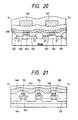
- Fig. 18 is a plan view of a memory cell portion
- Fig. 19 is a sectional view taken along a line X 3 X 3 ' of Fig. 18
- Fig. 20 is a sectional view taken along a line X 4 X 4 ' of Fig. 18,
- Fig. 21 is a sectional view taken along a line Y 3 Y 3 ' of Fig. 18.
- Figs. 18 to 21 denote the same regions as in Fig. 17, and a detailed description thereof will be omitted.
- This embodiment exemplifies a structure on a bulk Si substrate.
- the structure of this embodiment can also be manufactured on an SOI substrate.
- Wells in each two adjacent columns are isolated from each other by a selective oxide film 145, and floating gates in each two adjacent rows are isolated from each other by a thin selective oxide film 144.
- the buried bit lines are connected to metal wiring layers 146 and 147 for global bit lines at every 8 to 64 bits.
- Cells have floating gates 140 to 143.
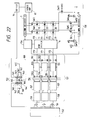
- the fifth embodiment of the present invention will be described below with reference to Fig. 22.
- the same reference numerals in Fig. 22 denote the same parts as in the above embodiments, and a detailed description thereof will be omitted.
- the circuit shown in Fig. 22 comprises a memory unit 150 described in the first embodiment, an SRAM unit 151, a scanning circuit 152 for sequentially reading out data from the SRAM, an EXOR circuit 153 for verifying the readout result of the memory of the present invention by comparing it with data from the SRAM, and a control circuit 154 for controlling the driving operation of the memory unit 150 in accordance with an output from the EXOR circuit.
- the SRAM unit 151 includes CMOS SRAM memory cell portions 155 which preferably comprise p-type MOS load memory cells since they require low consumption power.
- the SRAM unit 151 also includes MOS switches TR1, TR2, TR3, and TR4 for controlling the driving operations of the SRAM memory cells, common data lines 156, sense amplifiers 157, output buffers 158, and switches 159 for selecting the outputs from the output buffers.
- the EXOR circuit 153 comprises gates 160, 161, 166, 167, and 168, which are input to CMOS inverters via floating gates 162, p-type MOS transistors 163, and n-type MOS transistors 164.
- An output 165 from the first CMOS inverter is input to a gate 166 of the second CMOS inverter.
- An output 169 from the second CMOS inverter is input to the control circuit 154.
- Word lines 170, 171, and 172 are commonly arranged in the memory cell unit of the present invention, and the SRAM memory unit.
- Data are written in a desired column of the memory unit 150, and the same data are written in the SRAM cells in the SRAM memory unit 151.
- the memory unit 150 is set in a read mode, and the data in the column are sequentially read out using a sense amplifier 15.
- the scanning circuit 152 reads out the corresponding bits from the SRAM cells of the SRAM memory unit 151 via the sense amplifiers 157, and these readout outputs are input to the gates 160 and 161 of the EXOR circuit 153.
- the output from the EXOR circuit 153 changes to high level when the values input to the gates 160 and 161 are different from each other, and changes to low level when they are equal to each other, whether or not data are normally written in and read out from the memory unit 150 can be checked based on the output from the EXOR circuit 153.
- the EXOR circuit 153 is a CMOS circuit having multiple input gates via the floating gates, and can be manufactured based on a structure equivalent to that of the memory unit 150. In addition, the EXOR circuit 153 can realize high-performance processing using a smaller number of transistors. In this embodiment, an EXOR logic operation is executed.
- a majority logic of input data can be realized by two transistors (n-type and p-type MOS transistors). By utilizing this majority logic, parity check operations of input and readout 8-bit data can also be attained.
- At least one bit of a data string may be assigned as an error check bit of the data string, and is confirmed when the data string is read out.
- the SRAM memory unit has a memory size equal to that of one column of the memory unit 150.
- the present invention is not limited to this size.
- the memory size may be increased to a level as a buffer memory to achieve high-speed random access and write operations.
- the buffer memory comprises an SRAM.
- a DRAM, a flash memory, or the like may be arranged on a single chip to perform the above-mentioned operation.
- the above-mentioned arrangement of the fifth embodiment has the following merits.
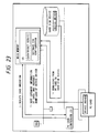
- the storage device of the present invention is applied to an external storage card (PC card) for, e.g., a personal computer.
- PC card an external storage card for, e.g., a personal computer.
- Fig. 23 is a diagram showing the relationship between a card and a system when the present invention is applied to a PC card.
- a device driver for a PC card to be used resides in a main memory.
- the number of device drives to be resided in the main memory unit increases, and some application software programs cannot operate due to the large total capacity of the resident device drivers.
- a ROM unit is also arranged on the chip to store the device driver of the card and CIS information (card-information-structure), i.e., the type and capacity of the card, identification information and configuration information of the card, and the like.
- CIS information card-information-structure
- the card of this embodiment has a function of notifying card insertion, and executing down-loading in accordance with a device driver down-load instruction, as shown in Fig. 12.
- An interface between the card and the main body has a 68-pin connector, and complies with a data bus width of 32 bits, a clock frequency of 16 MHz, a maximum data transfer rate of 60 Mbytes/s, and the like in accordance with the formats of PCMCIA (the standardization group in U.S.A.) and JEIDA (Japan Electronic Industry Development Association).
- the seventh embodiment of the present invention will be described below with reference to Fig. 24.
- the seventh embodiment is directed to an IC card which inputs/outputs information based on light.
- the IC card comprises a storage device 180 of the present invention, a battery 181, a semiconductor laser 182, a photodetector 185, a control circuit 186 for controlling the storage device mounted on a board 179, the laser, and the photodetector, a transparent resin package 183, and a lens 184.
- the IC card of the present invention exchanges all kinds of information to be exchanged with an external circuit such as data to be written, data to be read out, control clocks, and the like on the basis of light, and all the remaining functions are executed by the control circuit 186 arranged on the board 179.
- alignment marks for aligning an optical system are formed on the board 179.
- the IC card of this embodiment is set in a reader/writer of this card, the card is set at a desired position at high speed.
- the IC card of this embodiment has the following merits.
- the eighth embodiment of the present invention is directed to a storage device incorporating a programmable logic array in which the first poly-Si layer constituting the floating gates of the storage device of the present invention, and the second poly-Si layer constituting word lines are arranged in a matrix, a large number of AND gates and OR gates are arranged, and lines at each intersection of the matrix are changed from a high-resistance state to a low-resistance state to be substantially connected to each other, thereby freely setting a logic according to the intended application purpose of each user.
- the resistance between the lines can be changed to a low-resistance state in correspondence with the bias to be applied to lines arranged in a matrix.
- the storage device incorporates a programmable logic array
- an operation according to the specifications of each user can be realized without changing the mask, thus reducing cost and shortening the delivery period to users.
- the storage device of the present invention has the following effects: a larger capacity and a smaller cell area per bit than those of the conventional semiconductor storage device, permanently stable written information, low consumption voltage, low-voltage driving, storage and holding without any battery, high reliability, an easy driving method and high operability, high-speed read/write operations, a low error rate, wide use environments, a short manufacturing process, high yield, and high performance of a chip realized by integrating other types of storage devices, logic circuits, and the like as peripheral circuits on a single chip, and the like.
- the storage device of the present invention can be generally used not only as storage devices for computers but also as storage media for audio/video information, and can replace commercially available audio tapes, video tapes, CD-ROMs, and the like by utilizing higher performance characteristics than them.
- the storage device of the present invention is suitable for an external storage device for portable equipment, electronic publishing, a controller, and an electronic video/image memory, e.g., a system which stores an output from a still video camera, FAX, copy machine, or the like in a card constituted by the storage device of the present invention to allow a user to easily carry video data.
- the abbreviation 'GOLD' means Gate-drain Overlapped Lightly Doped drain.
Description
- The present invention relates to solid-state storage devices, particularly one-time programmable read only memory (OT-PROM) cells, arrays and circuits including the same, and methods for programming and reading such arrays.
- In recent years, along with the development of information/video industries, media and devices for storing information have been extensively developed. Of these media and devices, storage devices such as DRAMs, SRAMs, and the like have large storage capacities even though they have compact, lightweight, and low-power structure, and allow high-accuracy read/write operations at high speed. For these reasons, these devices are used in equipment in various fields.
- Also, recently, a storage device, so-called a flash memory, which is programmable and can hold information, has received a lot of attention. This storage device is superior to the DRAM in terms of the degree of integration.
- On the other hand, an OT-PROM (one time PROMs) in which information can be written only once has been proposed in Japanese Laid-Open Patent Application No. 62-188260 (inventor: Levi Gersburg (phonetic)) and Japanese Laid-Open Patent Application No. 62-49651 (inventors: Brian E. Cook, Douglas P. Berlet (phonetic)). In the arrangement of the OT-PROM, a wiring metal is connected in series with a main electrode (the source or drain for a MOSFET; the emitter for a bipolar transistor) of a transistor via an a-Si layer. By changing the a-Si layer from a high-resistance state to a low-resistance state, a storage operation is achieved.
- However, a storage device such as a DRAM using a semiconductor has the following problems.
- 1. Semiconductor storage devices represented by DRAMs and SRAMs suffer a high rate of chip cost increase along with an increase in storage capacity, and also suffer higher bit cost than those of floppy disks, magnetic tapes, and CD-ROMs. For these reasons, such a storage device cannot be actually used as a high store capacity storage medium.
- 2. At present, the storage capacity is at the 256-Mbit level even at the research level, and is insufficient as an information volume for images.
- 3. When information is stored in a DRAM or SRAM, the DRAM or SRAM must be kept supplied with a power supply voltage, and it is difficult to apply it to portable equipment. Under these circumstances, a battery built-in device is applied to such equipment.
-
- On the other hand, a flash memory which is superior to a DRAM in terms of degree of integration,also has the following problems.
- 1. Since a charge is written in or erased from a floating gate by injection of a Ford-Nordheiom (FN) tunnel current, hot electrons, or the like, the reliability of an insulating layer which is subjected to a charge input/output operation is degraded as the number of times of use increases.
- 2. The FN tunnel current density, J, is expressed
by:
- 3. The FN tunnel current strongly depends on the film quality and thickness of the insulating film, and the proper write or erase time undesirably varies among samples and bits. For this reason, in practice, after chips are manufactured, the chips are classified into a plurality of groups in an inspection process, and are operated at timings suitable for these groups. Thus, the load on the inspection process is heavy, resulting in high cost.
- 4. As the storage capacity increases, the floating gate area decreases. For this reason, the floating gate capacity decreases proportionally, and the floating gate potential changes largely even by a small leakage current. Therefore, in order to assure a desired capacity, an affordable reduction in floating gate area is limited, and this limitation disturbs an increase in capacity.
-
- Furthermore, the OT-PROM in which information can be written only once is excellent in that the state after information is written is permanent . However, one kind of OT-PROM has required an a-Si layer and a contact area between the a-Si layer and a wiring layer per bit. In a semiconductor process, formation of contact holes is difficult to achieve as compared to formation of line patterns. Even if a 0.8-µm rule process is used, the contact size is on the 1-µm2 order which is about 20% larger than 0.8 µm. Since the wiring width must be larger than each contact hole, the area per bit cannot be reduced. For these reasons, it is difficult to realize a large storage capacity in the proposed memories. Also, since a large current flows through the a-Si layer in a write operation, the consumption power is high, and it is difficult to apply such a memory to portable equipment.
- Another kind of OT-PROM is described in European Patent Application EP-A-0089457 in which there is disclosed a single gate PMOS transistor cell wherein the gate insulator has thinner and thicker portions adjacent the drain and the source, respectively. The gate electrode, channel and the thinner portion of the gate insulator adjacent to the drain serve as an antifuse which is irreversibly changeable from a high resistance state to a low resistance state.
- Yet another kind of OT-PROM is described in published Japanese Patent Application JP-A-51-147135. The principal features of the memory cell, a double insulated gate FET, are recited in the preamble of claim 1 attached. However, in the case of this published disclosure, the antifuse provided is constituted by the floating gate, the channel and a thinner portion of the floating gate insulator layer at the source end of the channel.
- The memory cell of the present invention is characterised in that:
the capacitance between the floating gate and the channel is greater than the capacitance between the control gate and the floating gate and the antifuse is formed of the control gate, the control gate insulator layer, and the floating gate. - Other aspects of the present invention include the memory arrays, circuits, and methods of programming and of reading such arrays as set forth in the appended claims.
- Insofar as in the arrays claimed an antifuse is provided in each cell at the intersection of each wordline and bit line, it is mentioned that there is disclosed a matrix wired array of antifuses in IEEE Electron Device Letters, Vol. 13, No. 1, January 1992 pages 53-55, the article "A Sublithographic Antifuse Structure for Field Programmable Gate Array Applications" by Chen, K.L. et al. A detailed description of antifuse construction is given therein.
- Insofar as the memory cell claimed is a transistor having a source, a drain, a channel, an insulated floating gate and an insulated control gate it is acknowledged that United States Patent US-A-4,332,077 discloses an EEPROM having the same. In the transistor cell described therein the control gate overlaps with both a portion of the floating gate and a portion of the channel at the drain end thereof. The capacitance between the floating gate and the channel is greater than that between the control gate and the floating gate. The memory cell is programmed by causing a transfer of charge between the floating gate and the channel by Ford-Norheim tunnelling. The control gate insulator remains insulative, having at all times a high resistance state. The same is true of the floating gate insulator.
- Since an ON current of a transistor does not flow via an anti-fuse unlike in a conventional anti-fuse ROM, an operation error caused by heat can be prevented, and high reliability can be guaranteed.
-
- Fig. 1 is a circuit diagram showing the circuit arrangement of a storage device according to the present invention;
- Fig. 2 is a timing chart showing the write operation according to the first embodiment of the present invention;
- Fig. 3 is a timing chart showing the read operation according to the first embodiment of the present invention;
- Fig. 4 is a plan view showing a cell portion according to the first embodiment of the present invention;
- Figs. 5A and 5B are sectional views showing the cell portion according to the first embodiment of the present invention;
- Figs. 6A to 6D are sectional views showing the processes in the manufacturing method according to the first embodiment of the present invention;
- Figs. 7A and 7B are sectional views showing a cell portion according to the second embodiment of the present invention;
- Figs. 8A to 8C are sectional views showing the processes in the manufacturing method according to the second embodiment of the present invention;
- Figs. 9A to 9C are respectively a plan view and sectional views showing a cell portion according to the third embodiment of the present invention;
- Fig. 10 is a perspective view showing a process in the manufacturing method according to the third embodiment of the present invention;
- Fig. 11 is a perspective view showing a process in the manufacturing method according to the third embodiment of the present invention;
- Fig. 12 is a perspective view showing a process in the manufacturing method according to the third embodiment of the present invention;
- Fig. 13 is a perspective view showing a process in the manufacturing method according to the third embodiment of the present invention;
- Fig. 14 is a perspective view showing a process in the manufacturing method according to the third embodiment of the present invention;
- Fig. 15 is a perspective view showing a process in the manufacturing method according to the third embodiment of the present invention;
- Fig. 16 is a perspective view showing a process in the manufacturing method according to the third embodiment of the present invention;
- Fig. 17 is a circuit diagram showing an equivalent circuit of a cell portion according to the fourth embodiment of the present invention;
- Fig. 18 is a plan view showing the cell portion according to the fourth embodiment of the present invention;
- Fig. 19 is a sectional view showing the cell portion according to the fourth embodiment of the present invention;
- Fig. 20 is a sectional view showing the cell portion according to the fourth embodiment of the present invention;
- Fig. 21 is a sectional view showing the cell portion according to the fourth embodiment of the present invention;
- Fig. 22 is a circuit diagram showing an equivalent circuit according to the fifth embodiment of the present invention;
- Fig. 23 is a block diagram of a system upon application to a PC card according to the sixth embodiment of the present invention; and
- Fig. 24 is a perspective view showing a storage device according to the seventh embodiment of the present invention.
-
- According to one preferred aspect of the present invention, source and drain semiconductor regions of a second conductivity type are formed each end of a channel semiconductor region of a first conductivity type, and a gate electrode structure is formed over the channel region. Furthermore, the gate electrode is designed to have a structure having two stacked gate electrodes, namely a floating gate and a control gate. In addition, by utilising the difference between the resistances between the stacked gate electrodes, information is stored.
- When the transistors are arranged in a matrix as needed, a large-capacity memory can be realized.
- As will be described later, by improving the structure of the transistor, the structure of the stacked gate electrode, and the like, the device performance can be further improved.
- The preferred embodiments of the present invention will be described in detail hereinafter with reference to the accompanying drawings.
- Fig. 1 shows an equivalent circuit of fundamental blocks of a storage device according to the present invention. The circuit shown in Fig. 1 has memory cells 11, 12, 13, 14, 21, 22, 23, 24, 31, 32, 33, 34, 41, 42, 43, and 44, and this embodiment exemplifies a 4 × 4 cell structure for the sake of simplicity (note that the detailed structure of each cell will be described in detail later).
- Each memory cell has a control gate 1 (serving as a floating gate 2, a channel 3, defined in a well or island, a source 5 and drain 6 forming thus a double insulated gate FET. The control gates of the memory cells of each row are connected via a word line 4. The sources and drains of the cells are connected in series with each other in units of columns. These cells are connected to a column decoder 7 as means for selecting each read column, a column decoder 8 as means for selecting each write bit line, a row driver 9 for driving each word line, a row decoder 10 for selecting each word line, a sense amplifier 15, and a buffer amplifier 16. Column address buffers 17 and 18 supply address inputs 20 to the column decoders 7 and 8. Switches SW1 to SW13 comprise MOSFETs. Of these switches, the switches SW9, SW10, SW12, and SW13 are ON/OFF-controlled by pulses 1, 2, 3, 4, and 5. The circuit receives a row address strobe signal (
RAS ) 26, a column address strobe signal (CAS ) 27, a write enable signal (WE ) 28, and an input data signal (DIN) 29, and outputs an output data signal (DOUT) 30. Note thatRAS ,CAS , andWE are shown in Fig. 1. - The operation of this storage device will be described below. In this device, two different address signals are time-divisionally input from a single input pin. After the column address is determined, the
CAS signal 27 changes from high level to low level to fetch the column address into the chip. After the row address is determined, theRAS signal 26 changes from high level to low level to fetch the row address into the chip. With this control, the number of address pins can be halved. Whether the chip is in a read or write mode is determined depending on high or low level of theWE signal 28. - In the read mode, after an elapse of a predetermined period of time from the change in
RAS signal, significant output data is obtained from a DOUT terminal 30. In the write mode, data is written from a DIN terminal 29. - The write operation will be described in detail below with reference to the timing chart shown in Fig. 2. The power supply voltage of this chip is set to be 3.3 V to achieve low power consumption. In Fig. 2, CG1, CG2, CG3, and CG4 represent the first, second, third, and fourth word line potentials in Fig. 1. Also, BL1, BL2, BL3, and BL4 represent the pulses respectively input to the switches SW5 to SW8 as n-MOSFETs. Fig. 2 exemplifies pulses generated when information is written in the cell 21 in the storage device of this embodiment. Before the write operation, the column decoder-1 8 respectively sets the pulses BL1, BL2, BL3, and BL4 at high level, low level, low level, and low level, thereby setting the switch SW5 in an ON state, and setting other switches SW6, SW7, and SW8 in an OFF state. In this state, the well potential of the first column having a write target cell is held at the GND level as the low-potential reference voltage, and the well potentials of the remaining second to fourth columns are set in a floating state.
- On the other hand, the switches SW9, SW10, SW11, SW12, and SW13 also comprise n-type MOSFETs, and pulses 1, 2, 3, 4, and 5 are respectively set at low level, high level, high level, high level, and low level, as shown in Fig. 2. The switches SW1 to SW4 comprise p-type MOSFETs, and all pulses from the column decoder-2 7 are set at low level, thereby holding the source and drain potentials of the respective cells at the GND potential as the low-potential reference voltage.
- Then, the row driver 9 applies a pulse with an amplitude of 10 V to only a word line connected to the write target cell 21. In this case, although the power supply voltage is 3.3 V, since no current flows, a high voltage can be easily generated by a booster circuit in the chip. Upon application of this write pulse, a bias of about 6.6 V is applied across the control gate 1 and the floating gate 2 of the cell 21, and the resistance between the control gate 1 and the floating gate 2 changes from a high-resistance state to a low-resistance state in several ten ns, thus completing the write operation. Even when the above-mentioned pulse is applied across the control gate and the floating gate of each of the cells 22, 23, and 24 connected to the same word line, since only a bias as low as about 0.1 to 0.5 V is applied across these gates, the resistance between the control gate and the floating gate of each cell remains in a high-resistance state. For this reason, no information is written in these cells. This is because the voltage is mainly applied to the well and the substrate and is not applied across the control gate and the floating gate since the switches SW6 to SW8 are set in an OFF state, and the well potentials of the second, third, and fourth columns are set in a floating state, as described above. After the completion of the write operation, the word line potential is reset to 0 V, as indicated by CG2 in Fig. 2.
- As has been described above, the storage device of the present invention is a novel one since the gate structure of the transistor provided to each cell has a stacked structure of a floating gate and a control gate, and the storage device achieves the write operation by changing the resistance between the floating gate and the control gate (to a low resistance) by a pulse applied to the control gate.
- The read operation of the present invention will be described below with reference to the timing chart shown in Fig. 3. The transistors constituting the respective cells are assumed to be p-type MOSFETs, and their threshold value is set to be -1.8 V. In this embodiment, each cell portion is assumed to be a p-type MOSFET but may be an n-type MOSFET.
- Assume that a column to be subjected to the read operation is the first column in Fig. 1, information has already been written in only the cell 21 in this column, and no information is written in other cells 11, 31, and 41.
- In order to read out information from the first column, the column decoder-2 7 applies pulses for setting the transistor of only the switch SW1 in an ON state, and setting the transistors of other switches SW2, SW3, and SW4 in an OFF state to the gates of the switches. In the read operation, the switches SW12, SW13, and SW5 are set in OFF, ON, and ON states, so that the well potential of the column to be subjected to the read operation is fixed at the highest potential when the cell transistor is a PMOS. Needless to say, when the cell transistor is an NMOS, the fixed well potential is the lowest potential.
- First, the pulse 1 is set at high level to pre-charge the source-drain paths of the cells 11, 21, 31, and 41 to VCC level. This operation can be achieved when all the word lines are set at 0 V and the p-type MOSFETs of the respective cells are set in an ON state. The pulse 1 is set at low level, and a pulse CG1 of an amplitude of 3.3 V is applied to a word line connected to the cell 11, as shown in Fig. 3, so as to read out information from the cell 11. Since no information is written in the cell 11, the floating potential is 1.1 V which is determined by dividing the capacitances of the control gate and the floating gate of the cell. As described above, the threshold value of the p-type MOSFET of this embodiment is set to be -1.8 V, and even when the above-mentioned pulse is applied, the p-type MOSFET of the cell 11 remains in an ON state. Therefore, when the pulse 3 is applied, since all the p-type MOSFETs of the first column are in an ON state, the output from the sense amplifier 15 decreases, as indicated by 35 in Fig. 3, and it is determined that no information is written in the cell 11. Next, the pulse 1 is applied again to pre-charge the cells, and thereafter, the pulse CG2 is set at high level to read out information from the cell 21. Since the pulse has an amplitude of 3.3 V, and information has already been written in the cell 21, the control gate and the floating gate of the cell 21 are connected to each other in a low-resistance state, and the pulse of 3.3 V is directly applied to the cell 21. Therefore, the p-MOSFET of the cell 21 is set in an OFF state. As a result, even when the pulse 3 is applied, the sense amplifier output is kept at high level, as indicated by 36 in Fig. 3, and it is determined that information is written in the cell 21. By repeating the same operation, the outputs from the cells 31 and 41 are at low level, as indicated by 37 and 38 in Fig. 3, and no information is written in these cells.
- After the read operation, the pulses 2, 3, and 4 are set at high level, and the pulses 1 and 5 are set at low level, thereby setting not only the control gates of the cells but also the sources, drains, and the wells of them at 0 V. With this operation, the floating gate potential is stably reset to 0 V as an initial state, thus preventing an operation error. More specifically, in a standby state, all the sources, drains, control gates, and wells are set at 0 V, and even when a small leakage current flows through the floating gate, the gate is always automatically reset to 0 V, thus stabilizing the operation.
- Note that a more stable write operation is assured if the following relations are satisfied:
CFG is the capacitance formed between the floating gate 2, and the source/drain region and the well region of the MOSFET, CCG is the capacitance formed between the floating gate 2 and the control gate 1, and V1 and V2 are the voltages to be applied to the control gate respectively in the write and read modes. - Fig. 4 is a plan view of the memory cell portion of the present invention. The cell portion comprises word lines 51, 52, and 53 consisting of poly-Si and W-polyside, p+-type layers 54 and 55 which form the sources and drains of the p-type MOSFETs, floating gates 56 and 57 consisting of poly-Si, and channel portions 58 of the p-type MOSFETs. Figs. 5A and 5B respectively show an X1-X1' section and a Y1-Y1' section of Fig. 4. The same reference numerals in Figs. 5A and 5B denote the same parts as in Fig. 4, and a detailed description thereof will be omitted.
- A gate insulating layer 59 for the p-type MOSFETs preferably consists of: a combination of a nitride film, and a thermal oxide film of Si or an oxide film formed by Lp-CVD to achieve a large capacity; a thermal oxynitride film formed in an atmosphere of O2, NH3, and N2O; or Ta2O5 with a high dielectric constant. In this embodiment, a 10 nm (100-Å) thick film with an effective dielectric constant of 5 was formed by combining an oxide film and a nitride film, and was used as the insulating film.
- The cell portion also comprises a p-type substrate 60, and a high-concentration n+-type layer 63 formed below the n-type well. When the number of p-type MOSFETs to be connected in series with each other is small, if the resistance of the n-type channel sufficient, the n+-type layer 63 is not always required. An insulating layer 61 is formed between the floating gate and the control gate. In this embodiment, a 5nm (50-Å) thick poly-Si film is formed to serve as the insulating film 61 by thermal oxidation of the floating gate. With this structure, the capacitance per unit area between the control gate and the floating gate is higher (about 1.5 times) than that between the floating gate and the lower Si layer. However, as can be seen from Figs. 4 to 5B, the floating gate is formed to have an area larger than the overlapping area of the control gate and the floating gate, and the practical capacitance between the floating gate and the underlying Si layer is set to be higher than that between the control gate and the floating gate. Thus, a desired voltage is applied across the control gate and the floating gate upon application of a write pulse.
- The method of manufacturing the structure according to the present invention will be described below with reference to Figs. 6A to 6D. Note that the same reference numerals in Figs. 6A to 6D denote the same parts as in Figs. 4 to 5B.
- As the p-type Si substrate 60, a substrate having an impurity concentration of 1014 to 1017 cm-3 can be used. In this case, in consideration of the width between wells to be divided, and the capacitance formed in each well, a substrate having an impurity concentration of 1016 cm-3 is preferable. As shown in Fig. 6A, a field oxide film 64 for element isolation is formed by a selective oxidation or modified selective oxidation method (when an Si film is oxidized after a groove is formed in the Si film where a field oxide film is to be formed by etching, the bird's beak is narrowed, and the isolation width can be decreased). Thereafter, patterning for forming the n-type well 58 is performed, and a well having an impurity concentration about 2 to 7 times the substrate concentration is formed by ion implantation. In this case, in order to assure the withstand voltage between adjacent n-type wells, the depth of the well is level with the bottom level of the field oxide film 64, i.e., the well is considerably shallower than a conventional one. In the next step, as shown in Fig. 6B, an 8.5 nm (85-Å) thick thermal oxide film is formed by Wet oxidation at 750°C to 1,100°C, and is subjected to a heat treatment in an NH3 atmosphere at 950°C to 1,100°C for 90 seconds, and in an O2 or N2O atmosphere at 1,150°C for 90 seconds, thus essentially forming an SiON film having a thickness of about 10 nm (100Å). Then, 400 nm (4,000-Å) thick poly-Si films 57 and 66 as the first layer are formed by Lp-CVD, and are subjected to ion implantation and annealing to dope an impurity in the poly-Si films. Thereafter, n+-type layers 65 serving as the source and drain of the n-type MOSFET, and p+-type layers 54 serving as the source and drain of the p-type MOSFET are formed. In order to relax electric fields at the source and drain terminals upon miniaturization, the n- and p-MOSFETs preferably have LDD and GOLD structures formed in low-temperature operations, respectively.
- Subsequently, as shown in Fig. 6B, the oxide film formed on the poly-Si surface is peeled using dilute hydrogen fluoride. After the peeling, a chemical oxide film having a thickness of about 1 nm (10Å) to 5 nm (50 Å) is formed in pure water added with ozone (O3), an acid (H2SO4, HCl) added with hydrogen peroxide water, or alkali (NH4OH), and is subjected to a heat treatment in a high-purity Ar or N2 atmosphere at 500°C to 600°C for 30 minutes. When the thickness of the oxide film is to be slightly increased, an O2 atmosphere is also mixed. With this operation, a very thin oxide film is formed although it has a thickness different from that formed by an impurity in the poly-Si surface of the first layer. On this wafer, a poly-Si film as the second layer is formed by Lp-CVD again. An impurity is then doped in the same manner as in the previous process, and the resultant structure is patterned to form the word lines 51. When the word line length is large, W-polyside or the like is preferably used to achieve a low resistance. Finally, as shown in Figs. 6C and 6D, an insulating interlayer 70 such as BPSG, a contact 67, a metal wiring line 68, a passivation film are formed as in a conventional LSI process, and the resultant structure is patterned to form a pad portion 69, thus completing the manufacturing process of this embodiment. The number of masks used for forming the structure of this embodiment is half or less that required for manufacturing conventional memories such as DRAMs, SRAMs, flash E2PROMs, and the like. Therefore, not only the area per bit is decreased, but also the processes are very simple, resulting in high yield and low cost. In the description of the manufacturing method of this structure, a single well structure has been exemplified. However, the present invention is not limited to this. The method of the present invention is also effective for a double well structure including n- and p-type wells, a structure formed with a channel stop layer in an isolation portion, and a structure adopting trench isolation in some cases.
- In this structure, as the insulating layer between the first and second poly-Si layers, the chemical oxide film is annealed at a low temperature (500°C to 600°C) to form a film which has a withstand voltage about half or less than that of a thermal oxide film of bulk Si, and suffers only small variation. In this case, when an oxygen ion-implantation film is formed on the surface of the first poly-Si layer, an oxide film having a defective layer containing oxygen is obtained, and the withstand voltage is lowered with high controllability. In this case, in place of a chemical oxide film, a thermal oxide film having a thickness of about 10 nm (100Å) may be formed to assure a desired withstand voltage, and the capacitance can be lowered as the film thickness can be increased.
- As described above, a memory according to the first embodiment of the present invention has the following merits:
- 1) The memory structure is simple, and the area of one cell portion is determined by only the word line and the patterning precision of an Si active layer. Therefore, since the area per cell can be equal to or smaller than that of a conventional memory without forming a contact, the bit cost can be lowered.
- 2) The number of masks required for forming this structure is about half that for DRAMs, SRAMs, flash RAMs, and the like, thus achieving further cost reduction. Also, since processes are simple, problems of dust, and pattern errors occur, thus improving the yield.
- 3) The write operation is achieved by breakdown of the insulating layer between the first and second poly-Si layers. Since the withstand voltage of the poly-Si oxide film is low due to the presence of the C-Si oxide film, and the withstand voltage can be stably set to be a desired value with high controllability upon combination with a new process technique such as a chemical oxidation method, or an oxygen doping method, write errors hardly occur.
- 4) Written information is permanent. Therefore, neither a power supply to be connected to a memory nor a complicated operation such as a refresh operation are required.
- 5) The write time is very short, several 10 ns or less
- 6) Since the read and write states do not so strongly depend on environmental conditions (flash memories, DRAMs, and the like strongly depend on a leakage current), application variations can be extensively explored.
-
- The second embodiment of the present invention will be described below with reference to Figs. 7A to 8C. An Si wafer was used as the substrate of the first embodiment, while in the second embodiment, an SOI substrate was used. Figs. 7A and 7B show the sectional structures (corresponding to Figs. 5A and 5B) of a memory cell portion, and Figs. 8A to 8C show the manufacturing method. Note that the same reference numerals in Figs. 7A to 8C denote the same parts as in Figs. 4 to 6D showing the first embodiment, and-a detailed description thereof will be omitted. An SOI substrate 71 can use a high-quality SOI wafer such as SIMOX, a laminated SOI wafer, an SOI wafer which is manufactured by laminating, on a wafer having an insulating layer surface, a wafer which is formed by forming a porous layer on an Si surface, and forming an epitaxial film on the porous surface, and the like. The conductivity type of the substrate may be either n or p conductivity type, as long as the bias of the substrate is controlled so as not to turn on a parasitic MOS transistor formed via an SOI oxide film 72 (a MOS transistor formed when the oxide film 72 is considered as a gate insulating layer). Transistors in the cell portion are isolated in an island pattern, as indicated by 76 in Fig. 7A.
- With this structure, an isolation width 73 in a direction parallel to the word lines can be smaller than that obtained using conventional selective oxidation or modified selective oxidation, and the area per bit can be further reduced. For this reason, the chip size can be reduced, thus attaining low cost and high yield.
- Adjacent wells are completely isolated by an insulating layer, and the operation can be stabilized.
- As can be seen from Figs. 7A and 7B, since a channel portion 76 and a floating gate portion 56 of a TFT in the cell portion are vertically stacked, a step between adjacent cells undesirably becomes large. For this reason, an insulating layer 74 for planarization is formed between adjacent cells, so that word lines 75 can be formed flat.
- In the structure of the second embodiment, since the insulating layer is formed below the well, the capacitance of the well can be smaller than that obtained when a bulk substrate is used. As a result, in the write mode, the voltage between the control gate and the floating gate can be reduced for a non-write bit, write errors hardly occur, and the margin of the structure process can be widened.
- The manufacturing method according to the second embodiment of the present invention will be described below with reference to Figs. 8A to 8C. After n-type wells 77 and p-type wells 78 are formed in corresponding regions on the SOI substrate 71, regions 79 and 80 where n- and p-type MOSFETs are to be manufactured are patterned. Then, the first poly-Si layer, and the sources and drains of the n- and p-type MOSFETs are formed following the same processes as in the first embodiment. After this, a TEOS insulating layer is formed, and is etched back to expose the upper portions of highest floating gates 57. After this, the oxide film on the surface of the first poly-Si layer is temporarily removed using dilute hydrogen fluoride, and a thin insulating layer is formed on the surface by chemical oxidation or low-temperature thermal oxidation, thus forming word lines 51. Thus, a planarized structure is obtained, and even when the pattern size of an upper metal wiring line 68 is reduced, high yield is attained.
- The third embodiment of the present invention will be described below with reference to Figs. 9A to 9C.
- Fig. 9A is a plan view of a memory cell, Fig. 9B shows an X2X2' section of this plan view, and Fig. 9C shows a Y2Y2' section of this plan view. The memory cell portion shown in Figs. 9A to 9C comprises word lines 91, 92, and 93, p+-type diffusion layers 94 and 95 which serve as the sources and drains of p-type MOSFETs which are NAND-connected, floating gates 96 and 97 of the MOSFETs, n-type well layers 98 and 99 of the MOSFETs, a p-type substrate 81, n+-type buried layers 82 and 83, a metal layer 101 (e.g., a Ta-based metal layer (Ta, TaN)) formed on the surface of each floating gate, and an insulating layer 102 including the metal. As can be seen from Figs. 9B and 9C, the floating gate 96 and 97 have opposing portions sandwiching the well layers 98 and 99 therebetween, respectively.
- The outstanding feature of this structure as compared with the first and second embodiments is that the floating gates 96 and 97 are formed to have a small two-dimensional size so as to further reduce the cell area per bit in practice, and this structure is suitable for high integration. The reason why this structure is realized is that the transistors in the cell portion have three-dimensional structures, as shown in Fig. 9B, and the floating gate capacitance can be increased by utilizing not only upper portions 103 of the transistors but also side wall portions 104.
- The second feature of the third embodiment will be described below.
- This structure performs an SOI operation unlike a conventional bulk FET since the channel portions 98 and 99 are controlled by the parallel floating gates 96 and 97. Thus, since the effective carrier mobility is high, a high-speed read operation can be attained. In addition, a short channel effect which occurs upon miniaturization of the transistors can be suppressed, and a compact structure can be easily realized. This is because the channels are controlled by the two side gates, a high electric field is hardly applied, and the potential can be controlled. Therefore, the floating gate capacitance can be increased while simply reducing the two-dimensional size of the floating gate, thus realizing miniaturization. In addition, this transistor structure is most suitable for miniaturization.
- As a problem of an SOI transistor, immediately after the transistor is switched from ON to OFF, the OFF operation is delayed by minority carriers remaining in the channel portion. However, in this structure, since the n+-type layer is formed immediately below the channel, and can prevent the minority carriers from remaining, a higher-speed memory operation can be realized.
- The third feature of the structure according to the third embodiment of the present invention is that the word lines 91 to 93 are patterned to have sizes larger than the floating gates 96 and 97. With this structure, upon patterning of the word lines, the surface of each floating gate can be prevented from being exposed to an etching plasma or the like, and the reliability of the insulating withstand voltage between the floating gates and the word lines can be further improved.
- The fourth feature of the structure according to the third embodiment of the present invention is that the floating gates 96 and 97 are polyside films consisting of TaSix to have a low resistance although each floating gate has a very small film thickness, and the high-quality insulating layer covering the metal is formed in self-alignment on the surface layer of each floating gate. In the memory structure of the present invention, the word line and the floating gate must be changed to a low-resistance state at a desired withstand voltage (e.g., 5 V), and a high-resistance state must be reliably maintained at 3 V. When the structure is adjusted to obtain a desired withstand voltage using a thin insulating layer, a leakage current begins to flow undesirably.
- Therefore, it is important to form a dense film having a wide bandgap and high insulating characteristics in at least a portion of the structure. In this case, a metal layer of Ta, TaN, Ni, or Zr,
or a polyside layer is formed on the surface of the first poly-Si layer serving as the floating gate, and an insulating layer covering the metal layer is formed before formation of the second poly-Si layer. With this structure, an insulating layer which can assure a desired withstand voltage and can reduce the leakage current by 50% or more as compared to a conventional structure can be formed. - As a result, the error rate of the memory can be further lowered, and a memory with high reliability and high stability can be realized.
- The method of manufacturing the memory according to the third embodiment of the present invention will be described below with reference to Figs. 10 to 16. Figs. 9A to 9C have exemplified a case wherein the memory structure is formed on a bulk Si substrate. However, since an equivalent structure can be formed even on an SOI substrate, and element isolation is facilitated, as has been described in the second embodiment, a description of the manufacturing method in Figs. 10 to 16 will be made using an SOI substrate. For the sake of descriptive simplicity, all cells are assumed to be p-type TFTs.
- As shown in Fig. 10, an n+-type layer serving as an n-type buried layer is formed on a region, where a p-type MOSFET is to be manufactured, on the surface of an SOI wafer 105. In this formation, an ion implantation method, as indicated by 106 in Fig. 10, a method in which an impurity is doped upon formation of a laminated wafer, or the like may be used. The film thickness of an Si layer which forms the n+-type layer is preferably as small as possible, e.g. several hundred nm (several thousand Å).
- As shown in Fig. 11, a 1-µm thick epitaxial film 108 is grown on an n+-type layer 107. Film growth is preferably performed at low temperature and at high speed to prevent an impurity from being redistributed or auto-doped from the n+-type layer. The epitaxial process may not often be required depending on the concentration of the epitaxial layer 108 since it increases cost.
- As shown in Fig. 12, the layers 107 and 108 are patterned by anisotropic etching except for a portion 109 serving as an active layer. As the resist patterning, patterning on the order of 0.35 µm can be realized using a phase shift mask, modified illumination, or the like in an i-line stepper. Also, a stepper using an ArF excimer laser, EB lithography, and the like are suitable for micropatterning.
- Subsequently, as shown in Fig. 13, an oxynitride film 110 is formed on the surface of the portion 109.
- After the Si surface is oxidized in an O2 atmosphere at 1,100°C for 50 seconds, it is then subjected to a treatment in an NH3 atmosphere at 900°C for 60 seconds and in an N2O atmosphere at 1,100°C for 30 seconds. After the insulating layer is formed, a poly-Si film serving as a floating gate and a metal layer are subsequently formed, as indicated by 111 in Fig. 13. More specifically, a 200 nm (2,000-Å) thick poly-Si film is formed at 620°C, and a 150 nm (1,500-Å) Ta film is grown thereon by sputtering. Then, phosphorus is ion-implanted in the surface of the Ta metal film, thus forming a Ta polyside layer containing metal Ta in its surface layer.
- In the next step, as indicated by 112 in Fig. 14, a floating gate is patterned. Using the resist mask for the floating gate, boron is ion-implanted, as indicated by 113 in Fig. 14, thereby forming the source and drain.
- Thereafter, as shown in Fig. 15, a TEOS layer 114 is formed, and after a resist is coated thereon, the layer is etched back to expose a surface 115 of the floating gate 112. After the exposed portion is washed to temporarily remove the insulating film on the surface layer containing Ta, the resultant structure is subjected to a heat treatment in an O2 atmosphere at 200°C to 400°C, thereby forming an insulating oxide film containing a Ta metal. In the formation of the insulating oxide film, a method which also uses plasma irradiation may be used. The treatment is performed at a pressure of 4 Pa (30 mtorr) and at a temperature of 450°C while supplying Ar and O2 gases at 300 and 8 sccm.
- As shown in Fig. 16, the second poly-Si layer of a word line 116 is patterned to cover the insulating oxide film on the floating gate surface. Thereafter, an insulating interlayer such as BPSG is formed, and a contact hole, a wiring metal, and a passivation insulating layer are formed. Finally, a pad is etched to complete the sample chip.
- In the above description, a structure in which a metal layer is stacked on the floating gate surface has been exemplified. Alternatively, an oxide film on a single poly-Si layer may be used as in the first and second embodiments.
- When a layer having the same conductivity type as that of the well layer and a higher concentration than the well layer is formed on an upper edge portion of the well layer, changes in threshold value at the edge portion, and withstand voltage errors at the edge portion can be effectively prevented.
- The fourth embodiment of the present invention will be described below with reference to Fig. 17 and Figs. 18 to 21. In the fourth embodiment, cells are arranged in a NOR matrix to improve characteristics associated with functions such as a random access function. Fig. 17 shows an equivalent circuit of several cells of a portion of the fourth embodiment. The circuit comprises buried bit lines 120 and 121, and buried source lines 122 and 123, which consist of diffusion layers. Contacts in units of cells are not formed to reduce each cell area. The bit and source lines are connected to a common source line 126 and main bit lines 127 and 128 via selection transistors 124 and 125 at a desired period according to an application, such as 8 bits, 32 bits, 64 bits, or the like. The circuit also comprises word lines 129, 130, and 131. A transistor 132 of the cell portion comprises an n-type MOSFET, and the diffusion layers of the source and drain have n+ conductivity type. P-type well layers 133 and 134 are arranged in units of columns, and each two adjacent columns are isolated from each other.
- The driving method for this device will be explained below. First, the write operation will be described. When a write bit is assumed to be the transistor cell 132 of Fig. 17, the buried source line 122, buried bit line 120, and p-type well 133 of this transistor are fixed at 0 V, and at least the well potentials (134 in Fig. 17) of other columns are set in a floating state. When a pulse of 10 V is applied to the word line 129, a voltage of about 6 V is applied across the floating gate of the transistor 132 and the word line 129, and the floating gate and the word line 129 change to a low-resistance state. On the other hand, only a bias of 1 V or less is applied across the floating gate of a transistor 135 and the word line 129 since the well 134 is set in the floating state, thus maintaining a high-resistance state. The respective word lines are simultaneously driven to achieve parallel write operations.
- The read operation will be described below. The threshold value of the n-type MOSFET is set at about 1.5 V. In the read operation, the well potentials of all the cells are fixed to be a lowest potential value, a voltage applied to a read word line is set at 2.0 V, and a voltage applied to non-read word lines is set at 0 V. Before reading, the respective bit lines are pre-charged to VDD = 2 V to turn off the bit line switches (transistors) 125, and a word line to be selected is set at 2 V. The effective gate bias of a written cell becomes 2 V, the channel is turned on, and the bit line is set at the source potential, e.g., 0 V. On the other hand, the effective gate bias of each non-written cell becomes 1.2 V equal to or lower than the threshold value, since it is subjected to capacitance division with the floating gate. As a result, the transistor of the cell is set in an OFF state, and the bit line is kept at VDD. A sense amplifier reads out changes in potential of these bit lines as in the first embodiment.
- The two-dimensional structure and sectional structure of the fourth embodiment will be explained below with reference to Figs. 18 to 21. Fig. 18 is a plan view of a memory cell portion, Fig. 19 is a sectional view taken along a line X3X3' of Fig. 18, Fig. 20 is a sectional view taken along a line X4X4' of Fig. 18, and Fig. 21 is a sectional view taken along a line Y3Y3' of Fig. 18.
- The same reference numerals in Figs. 18 to 21 denote the same regions as in Fig. 17, and a detailed description thereof will be omitted. This embodiment exemplifies a structure on a bulk Si substrate. However, as in the above-mentioned embodiments, the structure of this embodiment can also be manufactured on an SOI substrate. Wells in each two adjacent columns are isolated from each other by a selective oxide film 145, and floating gates in each two adjacent rows are isolated from each other by a thin selective oxide film 144. The buried bit lines are connected to metal wiring layers 146 and 147 for global bit lines at every 8 to 64 bits. Cells have floating gates 140 to 143.
- When the NOR matrix of the fourth embodiment is adopted, various read and write methods are realized, and the memory of this embodiment can be applied to various systems.
- The fifth embodiment of the present invention will be described below with reference to Fig. 22. The same reference numerals in Fig. 22 denote the same parts as in the above embodiments, and a detailed description thereof will be omitted. The circuit shown in Fig. 22 comprises a memory unit 150 described in the first embodiment, an SRAM unit 151, a scanning circuit 152 for sequentially reading out data from the SRAM, an EXOR circuit 153 for verifying the readout result of the memory of the present invention by comparing it with data from the SRAM, and a control circuit 154 for controlling the driving operation of the memory unit 150 in accordance with an output from the EXOR circuit. The SRAM unit 151 includes CMOS SRAM memory cell portions 155 which preferably comprise p-type MOS load memory cells since they require low consumption power. The SRAM unit 151 also includes MOS switches TR1, TR2, TR3, and TR4 for controlling the driving operations of the SRAM memory cells, common data lines 156, sense amplifiers 157, output buffers 158, and switches 159 for selecting the outputs from the output buffers. The EXOR circuit 153 comprises gates 160, 161, 166, 167, and 168, which are input to CMOS inverters via floating gates 162, p-type MOS transistors 163, and n-type MOS transistors 164. An output 165 from the first CMOS inverter is input to a gate 166 of the second CMOS inverter. An output 169 from the second CMOS inverter is input to the control circuit 154. Word lines 170, 171, and 172 are commonly arranged in the memory cell unit of the present invention, and the SRAM memory unit.
- The operation method of the fifth embodiment of the present invention will be described below. Data are written in a desired column of the memory unit 150, and the same data are written in the SRAM cells in the SRAM memory unit 151. The memory unit 150 is set in a read mode, and the data in the column are sequentially read out using a sense amplifier 15. In synchronism with this read operation, the scanning circuit 152 reads out the corresponding bits from the SRAM cells of the SRAM memory unit 151 via the sense amplifiers 157, and these readout outputs are input to the gates 160 and 161 of the EXOR circuit 153. Since the output from the EXOR circuit 153 changes to high level when the values input to the gates 160 and 161 are different from each other, and changes to low level when they are equal to each other, whether or not data are normally written in and read out from the memory unit 150 can be checked based on the output from the EXOR circuit 153.
- The EXOR circuit 153 is a CMOS circuit having multiple input gates via the floating gates, and can be manufactured based on a structure equivalent to that of the memory unit 150. In addition, the EXOR circuit 153 can realize high-performance processing using a smaller number of transistors. In this embodiment, an EXOR logic operation is executed. Alternatively, when input gates for 8-bit inputs are arranged via the floating gates to constitute the same CMOS inverters as above, a majority logic of input data can be realized by two transistors (n-type and p-type MOS transistors). By utilizing this majority logic, parity check operations of input and readout 8-bit data can also be attained.
- The description of the operation of the circuit shown in Fig. 22 will be continued. When an operation error is confirmed based on the output result 169, the SRAM data are written again in the next column of the memory unit 150. With this control, an operation for correcting write and read errors can be realized.
- At least one bit of a data string may be assigned as an error check bit of the data string, and is confirmed when the data string is read out.
- In the arrangement shown in Fig. 22, the SRAM memory unit has a memory size equal to that of one column of the memory unit 150. However, the present invention is not limited to this size. For example, the memory size may be increased to a level as a buffer memory to achieve high-speed random access and write operations. In the above description, the buffer memory comprises an SRAM. Alternatively, a DRAM, a flash memory, or the like may be arranged on a single chip to perform the above-mentioned operation.
- The above-mentioned arrangement of the fifth embodiment has the following merits.
- 1) The error rate is very low.
- 2) Whether or not data is normally written can be confirmed on the chip.
- 3) The logic circuit for performing confirmation can be manufactured to have the same structure as that of the memory of the present invention without adding any new processes.
- 4) The logic circuit can be constituted by a smaller number of transistors than conventional logic circuits. For this reason, since a peripheral circuit can be realized in a small area, low cost and high performance can be attained.
- 5) Since a memory (SRAM, DRAM, flash memory, or the like) having a structure different from the memory structure of the present invention is incorporated, high-speed random access and write operations can be realized.
-
- In the sixth embodiment of the present invention, the storage device of the present invention is applied to an external storage card (PC card) for, e.g., a personal computer.
- An application of the present invention will be explained below. Fig. 23 is a diagram showing the relationship between a card and a system when the present invention is applied to a PC card.
- In an existing notebook type personal computer or portable information communication equipment which can cope with a PC card, a device driver for a PC card to be used resides in a main memory. When a personal computer or portable information communication equipment uses a plurality of types of PC cards, the number of device drives to be resided in the main memory unit increases, and some application software programs cannot operate due to the large total capacity of the resident device drivers.
- In a card constituted by using the memory chip of the present invention, a ROM unit is also arranged on the chip to store the device driver of the card and CIS information (card-information-structure), i.e., the type and capacity of the card, identification information and configuration information of the card, and the like. Thus, the card of this embodiment has a function of notifying card insertion, and executing down-loading in accordance with a device driver down-load instruction, as shown in Fig. 12.
- An interface between the card and the main body has a 68-pin connector, and complies with a data bus width of 32 bits, a clock frequency of 16 MHz, a maximum data transfer rate of 60 Mbytes/s, and the like in accordance with the formats of PCMCIA (the standardization group in U.S.A.) and JEIDA (Japan Electronic Industry Development Association).
- The seventh embodiment of the present invention will be described below with reference to Fig. 24. The seventh embodiment is directed to an IC card which inputs/outputs information based on light. The IC card comprises a storage device 180 of the present invention, a battery 181, a semiconductor laser 182, a photodetector 185, a control circuit 186 for controlling the storage device mounted on a board 179, the laser, and the photodetector, a transparent resin package 183, and a lens 184. The IC card of the present invention exchanges all kinds of information to be exchanged with an external circuit such as data to be written, data to be read out, control clocks, and the like on the basis of light, and all the remaining functions are executed by the control circuit 186 arranged on the board 179.
- Although not shown in Fig. 24, alignment marks for aligning an optical system are formed on the board 179. When the IC card of this embodiment is set in a reader/writer of this card, the card is set at a desired position at high speed.
- The IC card of this embodiment has the following merits.
- 1) Unlike a conventional IC card, the card of this embodiment has high reliability since it is free from a problem of a contact error of contact pins, a problem of low reliability of pins, and the like.
- 2) IC card mounting can be realized with very low cost since the IC card comprises a transparent resin package obtained by simple integral molding.
- 3) Since the modulation frequency of the semiconductor laser is high, information can be input/output at a high bit rate, and low consumption power can be attained.
-
- The eighth embodiment of the present invention is directed to a storage device incorporating a programmable logic array in which the first poly-Si layer constituting the floating gates of the storage device of the present invention, and the second poly-Si layer constituting word lines are arranged in a matrix, a large number of AND gates and OR gates are arranged, and lines at each intersection of the matrix are changed from a high-resistance state to a low-resistance state to be substantially connected to each other, thereby freely setting a logic according to the intended application purpose of each user. The resistance between the lines can be changed to a low-resistance state in correspondence with the bias to be applied to lines arranged in a matrix.
- When the storage device incorporates a programmable logic array, an operation according to the specifications of each user can be realized without changing the mask, thus reducing cost and shortening the delivery period to users.
- The storage device of the present invention has the following effects: a larger capacity and a smaller cell area per bit than those of the conventional semiconductor storage device, permanently stable written information, low consumption voltage, low-voltage driving, storage and holding without any battery, high reliability, an easy driving method and high operability, high-speed read/write operations, a low error rate, wide use environments, a short manufacturing process, high yield, and high performance of a chip realized by integrating other types of storage devices, logic circuits, and the like as peripheral circuits on a single chip, and the like. The storage device of the present invention can be generally used not only as storage devices for computers but also as storage media for audio/video information, and can replace commercially available audio tapes, video tapes, CD-ROMs, and the like by utilizing higher performance characteristics than them. Also, the storage device of the present invention is suitable for an external storage device for portable equipment, electronic publishing, a controller, and an electronic video/image memory, e.g., a system which stores an output from a still video camera, FAX, copy machine, or the like in a card constituted by the storage device of the present invention to allow a user to easily carry video data.
- As used herein, the abbreviation 'GOLD' means Gate-drain Overlapped Lightly Doped drain.
Claims (26)
- A one-time programmable read only memory (OT-PROM) cell (11) comprising:characterised in that:a source (5;54;94);a drain (6;54;94);a channel (3;58;76;98) of opposite conductivity type to said source and drain;a floating gate (2; 56; 96) located over said channel;a floating gate insulator layer (59;104) disposed between said floating gate and said channel;a control gate (1;51;75-91) located over said floating gate; anda control gate insulator layer (61;101 & 102) disposed between said control gate and said floating gate;said cell having an antifuse (51,61,56;75,61,56;91, 101,102,96) which is convertible irreversibly from a high-resistance state to a low-resistance state;
the capacitance CFG between said floating gate (2;56;96) and said channel (3;58;76;98) is greater than the capacitance CCG between said control gate (1;51; 75;91) and said floating gate (2;56;96) and said antifuse (51,61,56; 75,61,56; 91,101,102,96) is formed of said control gate (1;51;75;91), said control gate insulator layer (61; 101 & 102), and said floating gate (2;56;96). - A cell according to claim 1 wherein the capacitance per unit area between said control gate (1;51;75;91) and said floating gate (2;56;96) is higher than that between said floating gate (2;56;96) and said channel (3;58;76;98), the area of said floating gate (2;56;96) thus being larger than the overlapping area of said control gate (1;51;75;91) and said floating gate(2;56;96).
- A cell according to claim 2 wherein said floating gate is interposed between said control gate and said channel leaving no area of direct overlap between said control gate and said channel.
- A cell according to any of claims 1 to 3 wherein said source and drain are defined in a well (58;133) region of a semiconductor substrate (60;-), said channel being a part of said well, extending between said source and said drain.
- A cell according to any of claims 1 to 3 wherein said source (54) and drain (54) are defined in an isolated portion (80) of a semiconductive active layer (77,78) on an insulative substrate (71), said channel being a part of said isolated portion (80) of said semiconductive active layer, extending between said source and said drain.
- A cell according to either of claims 4 or 5 wherein said floating gate insulator layer (104;113) and said floating gate (96;112) extend vertically down each side of said channel (98;108) to increase the capacitance therebetween.
- A cell according to any preceding claim wherein said floating gate insulator layer is of silicon oxynitride (SiON) and said floating gate is of doped polycrystalline silicon (poly-Si).
- A cell according to any preceding claim, being once programmed and having thus said antifuse in said low-resistance state.
- An OT-PROM memory array comprising:a plurality of memory cells (11-44) arranged in rows and columns, each cell being a cell as claimed in any one of the preceding claims 1 to 7;a plurality of word lines extending in parallel in the row direction, respective word lines connecting the control gates of the cells arranged in respective rows; anda plurality of bit lines extending in parallel in the column direction, respective bit lines connecting the channels of the cells arranged in respective columns.
- An array according to claim 9 wherein in each column the cells (11-41; 12-42, 13-43, 14-44) are connected in series.
- An array according to claim 10 wherein the adjacent cells in each column have a common source/drain electrode (54) therebetween.
- An array according to claim 9 wherein in each column the cells (11-41; 12-42, 13-43, 14-44) are connected in parallel, in each column the sources of the cells being connected to a source line (122,123) and the drains of the cells being connected to a drain line (120,121).
- An array according to claim 12 wherein in each column the sources are co-extensive and define the source line and the drains are co-extensive and define the drain line.
- An array according to any of claims 9 to 13 comprising as said plurality of memory cells, cells as claimed in either of claims 4 or 5, wherein in each column said wells (58;98) or said isolated regions (76;108) are co-extensive.
- An array according to claim 14 wherein said co-extensive wells (58;98) or isolated regions (108) are shunted with a higher concentration impurity semiconductor (63;82; 107) of the same conductivity type.
- An array according to any of claims 9 to 15 once programmed and having thus the antifuses of selected cells in said low-resistance state, and the antifuses of non-selected cells in said high-resistance state.
- A method of programming the array of any of claims 9 to 15 whereby the antifuse of a selected cell is changed from said high resistance state to said low resistance state, said method being performed by:-grounding the sources and the drains of all said cells;grounding the bit line of the column of cells including the selected cell;isolating the bit lines of the columns of cells not including the selected cell so that the channels thereof are at a floating potential; andapplying a writing pulse of voltage V1 to the wordline of the row of cells including the selected cell, whilst the wordlines of the rows of cells not including the selected cell are grounded, the pulse voltage V1 being related to the breakdown voltage VBD of the control gate insulating layer of the selected cell by the following inequality relationship:
- A memory programming circuit for performing the method of claim 17, said circuit comprising:the array of any of claims 9 to 15;a row decoder (10) and a row driver (9), cooperative therewith, for applying the pulse voltage V1 to the wordline of the row including the selected cell, and for grounding the wordlines of the rows not including the selected cell;a ground line (-,SW12);an array of switches (SW5-SW8) interposed between the bit lines of said array and said ground line;a column decoder (8) arranged to control said array of switches to ground the bit line of the column including the selected cell whilst isolating the bit lines of the columns not including the selected cell;grounding means (7, SW1-SW4, SW10,SW11) for grounding the sources and drains of all said cells; andaddress means (18 to 20) to supply the row and column addresses of the selected cell to said row decoder and said column decoder.
- A method of reading the array of claim 16 performed by:setting the bit-line of a selected column at supply voltage VCC;precharging the source and drain of each cell of the selected column to the supply voltage;applying a reading pulse of voltage V2 to the wordline of a selected row, wherein V2 satisfies the following inequalities:V2 > Vth; V2 < Vth (1 + CFG/CCG) where Vth is the threshold value of the transistor having the source, drain, channel and floating gate of the selected cell, grounding the end source or source line of the selected row; andsensing the voltage on the end drain or drainline to read the voltage of the cell included in the selected row and selected column.
- A memory reading circuit for performing the method of claim 19, said circuit comprising:the array of claim 16;a row decoder (10) and a row driver (9), cooperative therewith, for grounding the wordlines during precharging, for applying the reading pulse V2 to the wordline of the selected row, and for grounding the wordlines of the non-selected rows during reading;a sense line;a first switch array (SW1-SW4) interposed between said sense line and the end drains or drain lines of said array;a first column decoder (7) for controlling said first switch array to connect the end drains or draw line of a selected column to said sense line for precharging and for sensing;a common line connected to the end sources or sense lines;a channel bias line;a second switch array (SW5-SW8) interposed between the bit lines of said array and said channel bias line;a second column decoder (8) for controlling said second switch array to connect the bit line of the selected column to said channel bias line whilst isolating the bit lines of non-selected columns from said bit line; switching means (SW9-SW13) for switching the sense line to the supply voltage VCC for precharging, for isolating the sense line from supply voltage and from ground for sensing, and for grounding the sense line after sensing, for isolating the common line during precharging, and for grounding the common line during reading, for switching the channel bias line to supply voltage VCC for precharging and reading, and for grounding the channel bias line during resetting;control means (25) for controlling the operation of said switching means in accordance with the method of claim 19; and address means (17-20) to supply the row & column addresses of a selected cell to said row decoder and said first and second column decoders.
- A memory circuit for performing the method of each of claims 17 and 19, said circuit comprising:an array according to any of claims 9 to 15;a row decoder (10), and a row driver (9) cooperative therewith, for applying said voltages to the wordlines of selected rows and for grounding non-selected rows of said array;a sense line;a first array of switches (SW1-SW4) interposed between said sense line and the end drain or drain lines of the columns of said array;a first column decoder (7) for controlling said first array of switches;a common line connected to the end sources or source lines of said array;a channel bias line;a second array of switches (SW5-SW8) interposed between said channel bias line and the bit lines of the array;a second column decoder for controlling the second array of switches;address means to supply the row and column addresses of a selected cell to said row decoder and said first and second column decoders;switching means for isolating said sense line, common line and channel bias line from supply voltage VCC and ground, and for switching them to supply voltage VCC or ground; andcontrol means for co-ordinating operation of said address means and switching means in accordance with the method of claims 17 and 19.
- A memory circuit as claimed in claim 21 having said memory array (hereinafter said first memory array);a second memory array of SRAM, DRAM or flash memory type ;and means for writing and reading data therein;data input means for supplying same data to be written both in said first memory array and in said second memory array; anda comparator for comparing the results of reading said first and second memory arrays.
- A memory circuit according to claim 22 arranged for storing the results of comparison by said comparator in said first memory array.
- A memory circuit according to either of claims 22 or 23, wherein said memory circuit is a NOR logic gate comprised of transistors which are replicas of the cells of said first memory array.
- A memory circuit according to any preceding claim 18 to 24 mounted on a card.
- A memory circuit according to claim 25 having a light receiving element and a light-emitting element arranged for inputting and outputting information.
Applications Claiming Priority (3)
| Application Number | Priority Date | Filing Date | Title |
|---|---|---|---|
| JP9970894 | 1994-05-13 | ||
| JP9970894A JP3273582B2 (en) | 1994-05-13 | 1994-05-13 | Storage device |
| JP99708/94 | 1994-05-13 |
Publications (2)
| Publication Number | Publication Date |
|---|---|
| EP0682370A1 EP0682370A1 (en) | 1995-11-15 |
| EP0682370B1 true EP0682370B1 (en) | 2000-09-06 |
Family
ID=14254575
Family Applications (1)
| Application Number | Title | Priority Date | Filing Date |
|---|---|---|---|
| EP95303162A Expired - Lifetime EP0682370B1 (en) | 1994-05-13 | 1995-05-10 | Storage device |
Country Status (5)
| Country | Link |
|---|---|
| US (2) | US5808336A (en) |
| EP (1) | EP0682370B1 (en) |
| JP (1) | JP3273582B2 (en) |
| KR (1) | KR100209817B1 (en) |
| DE (1) | DE69518693T2 (en) |
Cited By (47)
| Publication number | Priority date | Publication date | Assignee | Title |
|---|---|---|---|---|
| EP1837900A3 (en) * | 2006-03-21 | 2008-10-15 | Semiconductor Energy Laboratory Co., Ltd. | Nonvolatile semiconductor memory device |
| US7683430B2 (en) | 2005-12-19 | 2010-03-23 | Innovative Silicon Isi Sa | Electrically floating body memory cell and array, and method of operating or controlling same |
| US7733693B2 (en) | 2003-05-13 | 2010-06-08 | Innovative Silicon Isi Sa | Semiconductor memory device and method of operating same |
| US7732816B2 (en) | 2001-06-18 | 2010-06-08 | Innovative Silicon Isi Sa | Semiconductor device |
| US7736959B2 (en) | 2003-07-22 | 2010-06-15 | Innovative Silicon Isi Sa | Integrated circuit device, and method of fabricating same |
| US7924630B2 (en) | 2008-10-15 | 2011-04-12 | Micron Technology, Inc. | Techniques for simultaneously driving a plurality of source lines |
| US7933142B2 (en) | 2006-05-02 | 2011-04-26 | Micron Technology, Inc. | Semiconductor memory cell and array using punch-through to program and read same |
| US7933140B2 (en) | 2008-10-02 | 2011-04-26 | Micron Technology, Inc. | Techniques for reducing a voltage swing |
| US7940559B2 (en) | 2006-04-07 | 2011-05-10 | Micron Technology, Inc. | Memory array having a programmable word length, and method of operating same |
| US7947543B2 (en) | 2008-09-25 | 2011-05-24 | Micron Technology, Inc. | Recessed gate silicon-on-insulator floating body device with self-aligned lateral isolation |
| US7957206B2 (en) | 2008-04-04 | 2011-06-07 | Micron Technology, Inc. | Read circuitry for an integrated circuit having memory cells and/or a memory cell array, and method of operating same |
| US7969779B2 (en) | 2006-07-11 | 2011-06-28 | Micron Technology, Inc. | Integrated circuit including memory array having a segmented bit line architecture and method of controlling and/or operating same |
| US8014195B2 (en) | 2008-02-06 | 2011-09-06 | Micron Technology, Inc. | Single transistor memory cell |
| US8064274B2 (en) | 2007-05-30 | 2011-11-22 | Micron Technology, Inc. | Integrated circuit having voltage generation circuitry for memory cell array, and method of operating and/or controlling same |
| US8069377B2 (en) | 2006-06-26 | 2011-11-29 | Micron Technology, Inc. | Integrated circuit having memory array including ECC and column redundancy and method of operating the same |
| US8085594B2 (en) | 2007-06-01 | 2011-12-27 | Micron Technology, Inc. | Reading technique for memory cell with electrically floating body transistor |
| US8139418B2 (en) | 2009-04-27 | 2012-03-20 | Micron Technology, Inc. | Techniques for controlling a direct injection semiconductor memory device |
| US8174881B2 (en) | 2009-11-24 | 2012-05-08 | Micron Technology, Inc. | Techniques for reducing disturbance in a semiconductor device |
| US8189376B2 (en) | 2008-02-08 | 2012-05-29 | Micron Technology, Inc. | Integrated circuit having memory cells including gate material having high work function, and method of manufacturing same |
| US8194487B2 (en) | 2007-09-17 | 2012-06-05 | Micron Technology, Inc. | Refreshing data of memory cells with electrically floating body transistors |
| US8199595B2 (en) | 2009-09-04 | 2012-06-12 | Micron Technology, Inc. | Techniques for sensing a semiconductor memory device |
| US8213226B2 (en) | 2008-12-05 | 2012-07-03 | Micron Technology, Inc. | Vertical transistor memory cell and array |
| US8223574B2 (en) | 2008-11-05 | 2012-07-17 | Micron Technology, Inc. | Techniques for block refreshing a semiconductor memory device |
| US8264041B2 (en) | 2007-01-26 | 2012-09-11 | Micron Technology, Inc. | Semiconductor device with electrically floating body |
| US8310893B2 (en) | 2009-12-16 | 2012-11-13 | Micron Technology, Inc. | Techniques for reducing impact of array disturbs in a semiconductor memory device |
| US8315099B2 (en) | 2009-07-27 | 2012-11-20 | Micron Technology, Inc. | Techniques for providing a direct injection semiconductor memory device |
| US8319294B2 (en) | 2009-02-18 | 2012-11-27 | Micron Technology, Inc. | Techniques for providing a source line plane |
| US8349662B2 (en) | 2007-12-11 | 2013-01-08 | Micron Technology, Inc. | Integrated circuit having memory cell array, and method of manufacturing same |
| US8369177B2 (en) | 2010-03-05 | 2013-02-05 | Micron Technology, Inc. | Techniques for reading from and/or writing to a semiconductor memory device |
| US8391060B2 (en) | 2000-04-27 | 2013-03-05 | Semiconductor Energy Laboratory Co., Ltd. | Nonvolatile memory and semiconductor device |
| US8411513B2 (en) | 2010-03-04 | 2013-04-02 | Micron Technology, Inc. | Techniques for providing a semiconductor memory device having hierarchical bit lines |
| US8411524B2 (en) | 2010-05-06 | 2013-04-02 | Micron Technology, Inc. | Techniques for refreshing a semiconductor memory device |
| US8416636B2 (en) | 2010-02-12 | 2013-04-09 | Micron Technology, Inc. | Techniques for controlling a semiconductor memory device |
| US8498157B2 (en) | 2009-05-22 | 2013-07-30 | Micron Technology, Inc. | Techniques for providing a direct injection semiconductor memory device |
| US8508994B2 (en) | 2009-04-30 | 2013-08-13 | Micron Technology, Inc. | Semiconductor device with floating gate and electrically floating body |
| US8518774B2 (en) | 2007-03-29 | 2013-08-27 | Micron Technology, Inc. | Manufacturing process for zero-capacitor random access memory circuits |
| US8531878B2 (en) | 2011-05-17 | 2013-09-10 | Micron Technology, Inc. | Techniques for providing a semiconductor memory device |
| US8537610B2 (en) | 2009-07-10 | 2013-09-17 | Micron Technology, Inc. | Techniques for providing a semiconductor memory device |
| US8536628B2 (en) | 2007-11-29 | 2013-09-17 | Micron Technology, Inc. | Integrated circuit having memory cell array including barriers, and method of manufacturing same |
| US8547738B2 (en) | 2010-03-15 | 2013-10-01 | Micron Technology, Inc. | Techniques for providing a semiconductor memory device |
| US8576631B2 (en) | 2010-03-04 | 2013-11-05 | Micron Technology, Inc. | Techniques for sensing a semiconductor memory device |
| US8710566B2 (en) | 2009-03-04 | 2014-04-29 | Micron Technology, Inc. | Techniques for forming a contact to a buried diffusion layer in a semiconductor memory device |
| US8729620B2 (en) | 2006-03-21 | 2014-05-20 | Semiconductor Energy Laboratory Co., Ltd. | Nonvolatile semiconductor memory device |
| US8748959B2 (en) | 2009-03-31 | 2014-06-10 | Micron Technology, Inc. | Semiconductor memory device |
| US8873283B2 (en) | 2005-09-07 | 2014-10-28 | Micron Technology, Inc. | Memory cell and memory cell array having an electrically floating body transistor, and methods of operating same |
| US9559216B2 (en) | 2011-06-06 | 2017-01-31 | Micron Technology, Inc. | Semiconductor memory device and method for biasing same |
| TWI751606B (en) * | 2019-09-17 | 2022-01-01 | 日商鎧俠股份有限公司 | Semiconductor storage device |
Families Citing this family (43)
| Publication number | Priority date | Publication date | Assignee | Title |
|---|---|---|---|---|
| US5485031A (en) | 1993-11-22 | 1996-01-16 | Actel Corporation | Antifuse structure suitable for VLSI application |
| JPH08222648A (en) * | 1995-02-14 | 1996-08-30 | Canon Inc | Memory |
| DE19530363A1 (en) * | 1995-08-18 | 1997-02-20 | Deutsche Telekom Ag | module |
| KR100248123B1 (en) * | 1997-03-04 | 2000-03-15 | 구본준 | Thin-film transistor and method for manufacturing thereof |
| US7196929B1 (en) | 1997-07-29 | 2007-03-27 | Micron Technology Inc | Method for operating a memory device having an amorphous silicon carbide gate insulator |
| US6031263A (en) | 1997-07-29 | 2000-02-29 | Micron Technology, Inc. | DEAPROM and transistor with gallium nitride or gallium aluminum nitride gate |
| US6965123B1 (en) * | 1997-07-29 | 2005-11-15 | Micron Technology, Inc. | Transistor with variable electron affinity gate and methods of fabrication and use |
| US6794255B1 (en) | 1997-07-29 | 2004-09-21 | Micron Technology, Inc. | Carburized silicon gate insulators for integrated circuits |
| US6746893B1 (en) | 1997-07-29 | 2004-06-08 | Micron Technology, Inc. | Transistor with variable electron affinity gate and methods of fabrication and use |
| US7154153B1 (en) | 1997-07-29 | 2006-12-26 | Micron Technology, Inc. | Memory device |
| US6936849B1 (en) | 1997-07-29 | 2005-08-30 | Micron Technology, Inc. | Silicon carbide gate transistor |
| FR2767219B1 (en) | 1997-08-08 | 1999-09-17 | Commissariat Energie Atomique | ELECTRICALLY COMPATIBLE PROGRAMMABLE AND ERASABLE NON-VOLATILE MEMORY DEVICE WITH A CMOS / SELF-MANUFACTURING PROCESS |
| JP3558510B2 (en) * | 1997-10-30 | 2004-08-25 | シャープ株式会社 | Nonvolatile semiconductor memory device |
| JP2000174148A (en) * | 1998-12-09 | 2000-06-23 | Mitsubishi Electric Corp | Nonvolatile semiconductor storage device and its manufacture |
| EP1703521A1 (en) * | 1999-02-01 | 2006-09-20 | Hitachi, Ltd. | Semiconductor integrated circuit and nonvolatile memory element |
| ATE344535T1 (en) * | 1999-07-06 | 2006-11-15 | Elmos Semiconductor Ag | CMOS COMPATIBLE SOI PROCESS |
| US6901006B1 (en) | 1999-07-14 | 2005-05-31 | Hitachi, Ltd. | Semiconductor integrated circuit device including first, second and third gates |
| JP2001070246A (en) * | 1999-09-02 | 2001-03-21 | Nidek Co Ltd | Ophthalmologic device |
| US6583902B1 (en) | 1999-12-09 | 2003-06-24 | Alvesta, Inc. | Modular fiber-optic transceiver |
| WO2001042801A1 (en) * | 1999-12-09 | 2001-06-14 | Alvesta, Inc. | Method and apparatus for combined alignment and heat drain of stacked processing stages |
| IT1311314B1 (en) * | 1999-12-14 | 2002-03-12 | St Microelectronics Srl | OPTIMIZED REPROGRAMMING METHOD FOR NON-VOLATILE MEMORY CELLS, IN PARTICULAR OF THE FLASH EEPROM TYPE. |
| US20020113268A1 (en) * | 2000-02-01 | 2002-08-22 | Jun Koyama | Nonvolatile memory, semiconductor device and method of manufacturing the same |
| US6552396B1 (en) * | 2000-03-14 | 2003-04-22 | International Business Machines Corporation | Matched transistors and methods for forming the same |
| TW442979B (en) * | 2000-04-28 | 2001-06-23 | Unipac Optoelectronics Corp | Manufacturing method of thin-film transistor |
| FR2809526B1 (en) * | 2000-05-24 | 2003-07-25 | St Microelectronics Sa | REDUCED ROM MEMORY |
| US6515889B1 (en) * | 2000-08-31 | 2003-02-04 | Micron Technology, Inc. | Junction-isolated depletion mode ferroelectric memory |
| US6350653B1 (en) | 2000-10-12 | 2002-02-26 | International Business Machines Corporation | Embedded DRAM on silicon-on-insulator substrate |
| US6774426B2 (en) * | 2000-12-19 | 2004-08-10 | Micron Technology, Inc. | Flash cell with trench source-line connection |
| DE60233486D1 (en) * | 2001-05-07 | 2009-10-08 | Advanced Micro Devices Inc | FLOATING GATE MEMORY BUILDING PART USING COMPOUND MOLECULAR MATERIAL |
| TW520506B (en) * | 2001-08-09 | 2003-02-11 | Macronix Int Co Ltd | Structure of non-volatile memory |
| US6882573B2 (en) * | 2002-08-13 | 2005-04-19 | General Semiconductor, Inc. | DMOS device with a programmable threshold voltage |
| JP3941943B2 (en) * | 2003-03-12 | 2007-07-11 | 力旺電子股▲ふん▼有限公司 | ROM |
| EP1818989A3 (en) * | 2006-02-10 | 2010-12-01 | Semiconductor Energy Laboratory Co., Ltd. | Nonvolatile semiconductor storage device and manufacturing method thereof |
| EP1837917A1 (en) * | 2006-03-21 | 2007-09-26 | Semiconductor Energy Laboratory Co., Ltd. | Nonvolatile semiconductor memory device |
| KR101488516B1 (en) * | 2006-03-21 | 2015-02-02 | 가부시키가이샤 한도오따이 에네루기 켄큐쇼 | Nonvolatile semiconductor memory device |
| US7786526B2 (en) * | 2006-03-31 | 2010-08-31 | Semiconductor Energy Laboratory Co., Ltd. | Nonvolatile semiconductor memory device |
| EP1840947A3 (en) * | 2006-03-31 | 2008-08-13 | Semiconductor Energy Laboratory Co., Ltd. | Nonvolatile semiconductor memory device |
| US8022460B2 (en) * | 2006-03-31 | 2011-09-20 | Semiconductor Energy Laboratory Co., Ltd. | Nonvolatile semiconductor memory device |
| US7554854B2 (en) * | 2006-03-31 | 2009-06-30 | Semiconductor Energy Laboratory Co., Ltd. | Method for deleting data from NAND type nonvolatile memory |
| US7285480B1 (en) * | 2006-04-07 | 2007-10-23 | International Business Machines Corporation | Integrated circuit chip with FETs having mixed body thicknesses and method of manufacture thereof |
| US8773933B2 (en) | 2012-03-16 | 2014-07-08 | Micron Technology, Inc. | Techniques for accessing memory cells |
| JP5545809B2 (en) * | 2009-10-19 | 2014-07-09 | 旭化成エレクトロニクス株式会社 | Manufacturing method of semiconductor device |
| US8394700B2 (en) * | 2010-04-22 | 2013-03-12 | Semiconductor Components Industries, Llc | Device including memory array and method thereof |
Family Cites Families (17)
| Publication number | Priority date | Publication date | Assignee | Title |
|---|---|---|---|---|
| US3422321A (en) * | 1966-06-20 | 1969-01-14 | Sperry Rand Corp | Oxygenated silicon nitride semiconductor devices and silane method for making same |
| JPS51147135A (en) * | 1975-06-12 | 1976-12-17 | Nec Corp | Non-voratile semiconductor memory |
| JPS607295B2 (en) | 1975-06-13 | 1985-02-23 | 株式会社日立製作所 | data processing equipment |
| US4332077A (en) * | 1979-08-10 | 1982-06-01 | Rca Corporation | Method of making electrically programmable control gate injected floating gate solid state memory transistor |
| EP0089457A3 (en) * | 1982-03-23 | 1986-01-22 | Texas Instruments Incorporated | Avalanche fuse element as programmable memory |
| DE3363683D1 (en) * | 1982-03-23 | 1986-07-03 | Badische Maschf Gmbh | Method and device for compacting foundry moulding sand |
| JPS6249651A (en) * | 1985-06-25 | 1987-03-04 | テキサス インスツルメンツインコ−ポレイテツド | Antifuse, making thereof, electrically programmable memory cell and programming thereof |
| JPS62188260A (en) | 1985-10-18 | 1987-08-17 | レヴイ ガ−ズバ−グ | Electrically programmable read only memory |
| JPS62188620A (en) * | 1986-02-10 | 1987-08-18 | Mitsubishi Heavy Ind Ltd | Controlling method of table shaft for nc hobbing machine |
| US4757359A (en) * | 1986-04-07 | 1988-07-12 | American Microsystems, Inc. | Thin oxide fuse |
| JPH088314B2 (en) * | 1989-10-11 | 1996-01-29 | 株式会社東芝 | Nonvolatile semiconductor memory device and manufacturing method thereof |
| US5331197A (en) * | 1991-04-23 | 1994-07-19 | Canon Kabushiki Kaisha | Semiconductor memory device including gate electrode sandwiching a channel region |
| JPH061095A (en) * | 1992-06-19 | 1994-01-11 | Toshiba Corp | Memory card |
| JPH06334155A (en) * | 1993-05-27 | 1994-12-02 | Sharp Corp | Semiconductor memory device and manufacture thereof |
| US5457652A (en) * | 1994-04-01 | 1995-10-10 | National Semiconductor Corporation | Low voltage EEPROM |
| JPH08222648A (en) * | 1995-02-14 | 1996-08-30 | Canon Inc | Memory |
| US5491657A (en) * | 1995-02-24 | 1996-02-13 | Advanced Micro Devices, Inc. | Method for bulk (or byte) charging and discharging an array of flash EEPROM memory cells |
-
1994
- 1994-05-13 JP JP9970894A patent/JP3273582B2/en not_active Expired - Fee Related
-
1995
- 1995-05-05 US US08/435,803 patent/US5808336A/en not_active Expired - Fee Related
- 1995-05-10 EP EP95303162A patent/EP0682370B1/en not_active Expired - Lifetime
- 1995-05-10 DE DE69518693T patent/DE69518693T2/en not_active Expired - Fee Related
- 1995-05-12 KR KR1019950011655A patent/KR100209817B1/en not_active IP Right Cessation
-
1998
- 1998-08-07 US US09/130,370 patent/US6324101B1/en not_active Expired - Fee Related
Cited By (63)
| Publication number | Priority date | Publication date | Assignee | Title |
|---|---|---|---|---|
| US8391060B2 (en) | 2000-04-27 | 2013-03-05 | Semiconductor Energy Laboratory Co., Ltd. | Nonvolatile memory and semiconductor device |
| US7732816B2 (en) | 2001-06-18 | 2010-06-08 | Innovative Silicon Isi Sa | Semiconductor device |
| US7733693B2 (en) | 2003-05-13 | 2010-06-08 | Innovative Silicon Isi Sa | Semiconductor memory device and method of operating same |
| US7736959B2 (en) | 2003-07-22 | 2010-06-15 | Innovative Silicon Isi Sa | Integrated circuit device, and method of fabricating same |
| US8873283B2 (en) | 2005-09-07 | 2014-10-28 | Micron Technology, Inc. | Memory cell and memory cell array having an electrically floating body transistor, and methods of operating same |
| US7683430B2 (en) | 2005-12-19 | 2010-03-23 | Innovative Silicon Isi Sa | Electrically floating body memory cell and array, and method of operating or controlling same |
| US8729620B2 (en) | 2006-03-21 | 2014-05-20 | Semiconductor Energy Laboratory Co., Ltd. | Nonvolatile semiconductor memory device |
| EP1837900A3 (en) * | 2006-03-21 | 2008-10-15 | Semiconductor Energy Laboratory Co., Ltd. | Nonvolatile semiconductor memory device |
| US8134867B2 (en) | 2006-04-07 | 2012-03-13 | Micron Technology, Inc. | Memory array having a programmable word length, and method of operating same |
| US7940559B2 (en) | 2006-04-07 | 2011-05-10 | Micron Technology, Inc. | Memory array having a programmable word length, and method of operating same |
| US7933142B2 (en) | 2006-05-02 | 2011-04-26 | Micron Technology, Inc. | Semiconductor memory cell and array using punch-through to program and read same |
| US8295078B2 (en) | 2006-05-02 | 2012-10-23 | Micron Technology, Inc. | Semiconductor memory cell and array using punch-through to program and read same |
| US8402326B2 (en) | 2006-06-26 | 2013-03-19 | Micron Technology, Inc. | Integrated circuit having memory array including ECC and column redundancy and method of operating same |
| US8069377B2 (en) | 2006-06-26 | 2011-11-29 | Micron Technology, Inc. | Integrated circuit having memory array including ECC and column redundancy and method of operating the same |
| US7969779B2 (en) | 2006-07-11 | 2011-06-28 | Micron Technology, Inc. | Integrated circuit including memory array having a segmented bit line architecture and method of controlling and/or operating same |
| US8395937B2 (en) | 2006-07-11 | 2013-03-12 | Micron Technology, Inc. | Integrated circuit including memory array having a segmented bit line architecture and method of controlling and/or operating same |
| US8264041B2 (en) | 2007-01-26 | 2012-09-11 | Micron Technology, Inc. | Semiconductor device with electrically floating body |
| US8518774B2 (en) | 2007-03-29 | 2013-08-27 | Micron Technology, Inc. | Manufacturing process for zero-capacitor random access memory circuits |
| US8064274B2 (en) | 2007-05-30 | 2011-11-22 | Micron Technology, Inc. | Integrated circuit having voltage generation circuitry for memory cell array, and method of operating and/or controlling same |
| US8659948B2 (en) | 2007-06-01 | 2014-02-25 | Micron Technology, Inc. | Techniques for reading a memory cell with electrically floating body transistor |
| US8085594B2 (en) | 2007-06-01 | 2011-12-27 | Micron Technology, Inc. | Reading technique for memory cell with electrically floating body transistor |
| US8194487B2 (en) | 2007-09-17 | 2012-06-05 | Micron Technology, Inc. | Refreshing data of memory cells with electrically floating body transistors |
| US8446794B2 (en) | 2007-09-17 | 2013-05-21 | Micron Technology, Inc. | Refreshing data of memory cells with electrically floating body transistors |
| US8536628B2 (en) | 2007-11-29 | 2013-09-17 | Micron Technology, Inc. | Integrated circuit having memory cell array including barriers, and method of manufacturing same |
| US8349662B2 (en) | 2007-12-11 | 2013-01-08 | Micron Technology, Inc. | Integrated circuit having memory cell array, and method of manufacturing same |
| US8014195B2 (en) | 2008-02-06 | 2011-09-06 | Micron Technology, Inc. | Single transistor memory cell |
| US8325515B2 (en) | 2008-02-06 | 2012-12-04 | Micron Technology, Inc. | Integrated circuit device |
| US8189376B2 (en) | 2008-02-08 | 2012-05-29 | Micron Technology, Inc. | Integrated circuit having memory cells including gate material having high work function, and method of manufacturing same |
| US8274849B2 (en) | 2008-04-04 | 2012-09-25 | Micron Technology, Inc. | Read circuitry for an integrated circuit having memory cells and/or a memory cell array, and method of operating same |
| US7957206B2 (en) | 2008-04-04 | 2011-06-07 | Micron Technology, Inc. | Read circuitry for an integrated circuit having memory cells and/or a memory cell array, and method of operating same |
| US7947543B2 (en) | 2008-09-25 | 2011-05-24 | Micron Technology, Inc. | Recessed gate silicon-on-insulator floating body device with self-aligned lateral isolation |
| US8790968B2 (en) | 2008-09-25 | 2014-07-29 | Micron Technology, Inc. | Recessed gate silicon-on-insulator floating body device with self-aligned lateral isolation |
| US8315083B2 (en) | 2008-10-02 | 2012-11-20 | Micron Technology Inc. | Techniques for reducing a voltage swing |
| US7933140B2 (en) | 2008-10-02 | 2011-04-26 | Micron Technology, Inc. | Techniques for reducing a voltage swing |
| US7924630B2 (en) | 2008-10-15 | 2011-04-12 | Micron Technology, Inc. | Techniques for simultaneously driving a plurality of source lines |
| US8223574B2 (en) | 2008-11-05 | 2012-07-17 | Micron Technology, Inc. | Techniques for block refreshing a semiconductor memory device |
| US8213226B2 (en) | 2008-12-05 | 2012-07-03 | Micron Technology, Inc. | Vertical transistor memory cell and array |
| US8319294B2 (en) | 2009-02-18 | 2012-11-27 | Micron Technology, Inc. | Techniques for providing a source line plane |
| US8710566B2 (en) | 2009-03-04 | 2014-04-29 | Micron Technology, Inc. | Techniques for forming a contact to a buried diffusion layer in a semiconductor memory device |
| US8748959B2 (en) | 2009-03-31 | 2014-06-10 | Micron Technology, Inc. | Semiconductor memory device |
| US8400811B2 (en) | 2009-04-27 | 2013-03-19 | Micron Technology, Inc. | Techniques for providing a direct injection semiconductor memory device having ganged carrier injection lines |
| US8351266B2 (en) | 2009-04-27 | 2013-01-08 | Micron Technology, Inc. | Techniques for controlling a direct injection semiconductor memory device |
| US8139418B2 (en) | 2009-04-27 | 2012-03-20 | Micron Technology, Inc. | Techniques for controlling a direct injection semiconductor memory device |
| US8508970B2 (en) | 2009-04-27 | 2013-08-13 | Micron Technology, Inc. | Techniques for providing a direct injection semiconductor memory device |
| US8508994B2 (en) | 2009-04-30 | 2013-08-13 | Micron Technology, Inc. | Semiconductor device with floating gate and electrically floating body |
| US8498157B2 (en) | 2009-05-22 | 2013-07-30 | Micron Technology, Inc. | Techniques for providing a direct injection semiconductor memory device |
| US8537610B2 (en) | 2009-07-10 | 2013-09-17 | Micron Technology, Inc. | Techniques for providing a semiconductor memory device |
| US9076543B2 (en) | 2009-07-27 | 2015-07-07 | Micron Technology, Inc. | Techniques for providing a direct injection semiconductor memory device |
| US8587996B2 (en) | 2009-07-27 | 2013-11-19 | Micron Technology, Inc. | Techniques for providing a direct injection semiconductor memory device |
| US8315099B2 (en) | 2009-07-27 | 2012-11-20 | Micron Technology, Inc. | Techniques for providing a direct injection semiconductor memory device |
| US8199595B2 (en) | 2009-09-04 | 2012-06-12 | Micron Technology, Inc. | Techniques for sensing a semiconductor memory device |
| US8174881B2 (en) | 2009-11-24 | 2012-05-08 | Micron Technology, Inc. | Techniques for reducing disturbance in a semiconductor device |
| US8310893B2 (en) | 2009-12-16 | 2012-11-13 | Micron Technology, Inc. | Techniques for reducing impact of array disturbs in a semiconductor memory device |
| US8416636B2 (en) | 2010-02-12 | 2013-04-09 | Micron Technology, Inc. | Techniques for controlling a semiconductor memory device |
| US8411513B2 (en) | 2010-03-04 | 2013-04-02 | Micron Technology, Inc. | Techniques for providing a semiconductor memory device having hierarchical bit lines |
| US8576631B2 (en) | 2010-03-04 | 2013-11-05 | Micron Technology, Inc. | Techniques for sensing a semiconductor memory device |
| US8369177B2 (en) | 2010-03-05 | 2013-02-05 | Micron Technology, Inc. | Techniques for reading from and/or writing to a semiconductor memory device |
| US8547738B2 (en) | 2010-03-15 | 2013-10-01 | Micron Technology, Inc. | Techniques for providing a semiconductor memory device |
| US8411524B2 (en) | 2010-05-06 | 2013-04-02 | Micron Technology, Inc. | Techniques for refreshing a semiconductor memory device |
| US8630126B2 (en) | 2010-05-06 | 2014-01-14 | Micron Technology, Inc. | Techniques for refreshing a semiconductor memory device |
| US8531878B2 (en) | 2011-05-17 | 2013-09-10 | Micron Technology, Inc. | Techniques for providing a semiconductor memory device |
| US9559216B2 (en) | 2011-06-06 | 2017-01-31 | Micron Technology, Inc. | Semiconductor memory device and method for biasing same |
| TWI751606B (en) * | 2019-09-17 | 2022-01-01 | 日商鎧俠股份有限公司 | Semiconductor storage device |
Also Published As
| Publication number | Publication date |
|---|---|
| KR100209817B1 (en) | 1999-07-15 |
| JP3273582B2 (en) | 2002-04-08 |
| KR950034801A (en) | 1995-12-28 |
| US6324101B1 (en) | 2001-11-27 |
| US5808336A (en) | 1998-09-15 |
| JPH07307400A (en) | 1995-11-21 |
| EP0682370A1 (en) | 1995-11-15 |
| DE69518693T2 (en) | 2001-05-31 |
| DE69518693D1 (en) | 2000-10-12 |
Similar Documents
| Publication | Publication Date | Title |
|---|---|---|
| EP0682370B1 (en) | Storage device | |
| KR100234502B1 (en) | Semiconductor memory device | |
| US7622355B2 (en) | Write once read only memory employing charge trapping in insulators | |
| US7369435B2 (en) | Write once read only memory employing floating gates | |
| US7230848B2 (en) | Vertical NROM having a storage density of 1 bit per 1F2 | |
| US7257022B2 (en) | Nanocrystal write once read only memory for archival storage | |
| JP3118063B2 (en) | Nonvolatile storage element, nonvolatile storage device using the same, and method of manufacturing nonvolatile storage element | |
| US6952362B2 (en) | Ferroelectric write once read only memory for archival storage | |
| EP0908954B1 (en) | Semiconductor memory device and manufacturing method thereof | |
| US7110297B2 (en) | Semiconductor storage device and mobile electronic apparatus | |
| US6121079A (en) | Method for manufacturing a semiconductor memory device | |
| US6825527B2 (en) | Semiconductor memory device and manufacturing method | |
| JPH05205487A (en) | Nonvolatile storage element and nonvolatile storage device employing these elements and driving method of the device | |
| JPH05206411A (en) | Nonvolatile memory element and nonvolatile memory device utilizing the same as well as driving method of nonvolatile memory device | |
| JP3155816B2 (en) | Nonvolatile storage element, nonvolatile storage device using the same, and method of driving nonvolatile storage device |
Legal Events
| Date | Code | Title | Description |
|---|---|---|---|
| PUAI | Public reference made under article 153(3) epc to a published international application that has entered the european phase |
Free format text: ORIGINAL CODE: 0009012 |
|
| AK | Designated contracting states |
Kind code of ref document: A1 Designated state(s): DE FR GB IT NL |
|
| 17P | Request for examination filed |
Effective date: 19960328 |
|
| 17Q | First examination report despatched |
Effective date: 19980616 |
|
| GRAG | Despatch of communication of intention to grant |
Free format text: ORIGINAL CODE: EPIDOS AGRA |
|
| GRAG | Despatch of communication of intention to grant |
Free format text: ORIGINAL CODE: EPIDOS AGRA |
|
| GRAH | Despatch of communication of intention to grant a patent |
Free format text: ORIGINAL CODE: EPIDOS IGRA |
|
| GRAH | Despatch of communication of intention to grant a patent |
Free format text: ORIGINAL CODE: EPIDOS IGRA |
|
| GRAA | (expected) grant |
Free format text: ORIGINAL CODE: 0009210 |
|
| AK | Designated contracting states |
Kind code of ref document: B1 Designated state(s): DE FR GB IT NL |
|
| REF | Corresponds to: |
Ref document number: 69518693 Country of ref document: DE Date of ref document: 20001012 |
|
| ITF | It: translation for a ep patent filed |
Owner name: SOCIETA' ITALIANA BREVETTI S.P.A. |
|
| ET | Fr: translation filed | ||
| PLBE | No opposition filed within time limit |
Free format text: ORIGINAL CODE: 0009261 |
|
| STAA | Information on the status of an ep patent application or granted ep patent |
Free format text: STATUS: NO OPPOSITION FILED WITHIN TIME LIMIT |
|
| 26N | No opposition filed | ||
| REG | Reference to a national code |
Ref country code: GB Ref legal event code: IF02 |
|
| PGFP | Annual fee paid to national office [announced via postgrant information from national office to epo] |
Ref country code: GB Payment date: 20050426 Year of fee payment: 11 |
|
| PGFP | Annual fee paid to national office [announced via postgrant information from national office to epo] |
Ref country code: NL Payment date: 20050513 Year of fee payment: 11 |
|
| PGFP | Annual fee paid to national office [announced via postgrant information from national office to epo] |
Ref country code: FR Payment date: 20050520 Year of fee payment: 11 |
|
| PGFP | Annual fee paid to national office [announced via postgrant information from national office to epo] |
Ref country code: DE Payment date: 20050720 Year of fee payment: 11 |
|
| PG25 | Lapsed in a contracting state [announced via postgrant information from national office to epo] |
Ref country code: GB Free format text: LAPSE BECAUSE OF NON-PAYMENT OF DUE FEES Effective date: 20060510 |
|
| PGFP | Annual fee paid to national office [announced via postgrant information from national office to epo] |
Ref country code: IT Payment date: 20060531 Year of fee payment: 12 |
|
| PG25 | Lapsed in a contracting state [announced via postgrant information from national office to epo] |
Ref country code: NL Free format text: LAPSE BECAUSE OF NON-PAYMENT OF DUE FEES Effective date: 20061201 Ref country code: DE Free format text: LAPSE BECAUSE OF NON-PAYMENT OF DUE FEES Effective date: 20061201 |
|
| GBPC | Gb: european patent ceased through non-payment of renewal fee |
Effective date: 20060510 |
|
| NLV4 | Nl: lapsed or anulled due to non-payment of the annual fee |
Effective date: 20061201 |
|
| REG | Reference to a national code |
Ref country code: FR Ref legal event code: ST Effective date: 20070131 |
|
| PG25 | Lapsed in a contracting state [announced via postgrant information from national office to epo] |
Ref country code: FR Free format text: LAPSE BECAUSE OF NON-PAYMENT OF DUE FEES Effective date: 20060531 |
|
| PG25 | Lapsed in a contracting state [announced via postgrant information from national office to epo] |
Ref country code: IT Free format text: LAPSE BECAUSE OF NON-PAYMENT OF DUE FEES Effective date: 20070510 |