EP0683406A1 - Color filter, manufacturing method, and liquid crystal display - Google Patents
Color filter, manufacturing method, and liquid crystal display Download PDFInfo
- Publication number
- EP0683406A1 EP0683406A1 EP95303358A EP95303358A EP0683406A1 EP 0683406 A1 EP0683406 A1 EP 0683406A1 EP 95303358 A EP95303358 A EP 95303358A EP 95303358 A EP95303358 A EP 95303358A EP 0683406 A1 EP0683406 A1 EP 0683406A1
- Authority
- EP
- European Patent Office
- Prior art keywords
- ink
- layer
- colored
- color filter
- color
- Prior art date
- Legal status (The legal status is an assumption and is not a legal conclusion. Google has not performed a legal analysis and makes no representation as to the accuracy of the status listed.)
- Granted
Links
Images


Classifications
-
- G—PHYSICS
- G02—OPTICS
- G02F—OPTICAL DEVICES OR ARRANGEMENTS FOR THE CONTROL OF LIGHT BY MODIFICATION OF THE OPTICAL PROPERTIES OF THE MEDIA OF THE ELEMENTS INVOLVED THEREIN; NON-LINEAR OPTICS; FREQUENCY-CHANGING OF LIGHT; OPTICAL LOGIC ELEMENTS; OPTICAL ANALOGUE/DIGITAL CONVERTERS
- G02F1/00—Devices or arrangements for the control of the intensity, colour, phase, polarisation or direction of light arriving from an independent light source, e.g. switching, gating or modulating; Non-linear optics
- G02F1/01—Devices or arrangements for the control of the intensity, colour, phase, polarisation or direction of light arriving from an independent light source, e.g. switching, gating or modulating; Non-linear optics for the control of the intensity, phase, polarisation or colour
- G02F1/13—Devices or arrangements for the control of the intensity, colour, phase, polarisation or direction of light arriving from an independent light source, e.g. switching, gating or modulating; Non-linear optics for the control of the intensity, phase, polarisation or colour based on liquid crystals, e.g. single liquid crystal display cells
- G02F1/133—Constructional arrangements; Operation of liquid crystal cells; Circuit arrangements
- G02F1/1333—Constructional arrangements; Manufacturing methods
- G02F1/1335—Structural association of cells with optical devices, e.g. polarisers or reflectors
- G02F1/133509—Filters, e.g. light shielding masks
- G02F1/133514—Colour filters
- G02F1/133516—Methods for their manufacture, e.g. printing, electro-deposition or photolithography
-
- B—PERFORMING OPERATIONS; TRANSPORTING
- B41—PRINTING; LINING MACHINES; TYPEWRITERS; STAMPS
- B41J—TYPEWRITERS; SELECTIVE PRINTING MECHANISMS, i.e. MECHANISMS PRINTING OTHERWISE THAN FROM A FORME; CORRECTION OF TYPOGRAPHICAL ERRORS
- B41J2/00—Typewriters or selective printing mechanisms characterised by the printing or marking process for which they are designed
- B41J2/005—Typewriters or selective printing mechanisms characterised by the printing or marking process for which they are designed characterised by bringing liquid or particles selectively into contact with a printing material
- B41J2/01—Ink jet
-
- G—PHYSICS
- G02—OPTICS
- G02B—OPTICAL ELEMENTS, SYSTEMS OR APPARATUS
- G02B5/00—Optical elements other than lenses
- G02B5/20—Filters
- G02B5/201—Filters in the form of arrays
-
- B—PERFORMING OPERATIONS; TRANSPORTING
- B41—PRINTING; LINING MACHINES; TYPEWRITERS; STAMPS
- B41J—TYPEWRITERS; SELECTIVE PRINTING MECHANISMS, i.e. MECHANISMS PRINTING OTHERWISE THAN FROM A FORME; CORRECTION OF TYPOGRAPHICAL ERRORS
- B41J2202/00—Embodiments of or processes related to ink-jet or thermal heads
- B41J2202/01—Embodiments of or processes related to ink-jet heads
- B41J2202/09—Ink jet technology used for manufacturing optical filters
Definitions
- the present invention relates to a method of manufacturing a color filter by forming and arranging a plurality of colored filter elements on a transparent substrate, the color filter, a liquid crystal display apparatus, and an apparatus having the liquid crystal display apparatus.
- the first method is a coloring method, which is the most popular method.
- a water-soluble polymer material as a colorable material is coated on a glass substrate, and the coating is patterned into a desired shape by a photolithography process. The obtained pattern is dipped in a color bath to obtain a colored pattern. This process is repeated three times to form R, G, and B color filter layers.
- the second method is a pigment dispersion method, which is currently replacing the coloring method.
- a pigment-dispersed photosensitive resin layer is formed on a substrate and patterned into a single-color pattern. This process is repeated three times to obtain R, G, and B color filter layers.
- the third method is an electrodeposition method.
- a transparent electrode is patterned on a substrate, and the resultant structure is dipped in an electrodeposition coating fluid containing a pigment, a resin, an electrolyte, and the like to be colored in the first color by electrodeposition. This process is repeated three times to form R, G, and B color filter layers. Finally, these layers are calcined.
- the fourth method is a method of dispersing a pigment in a thermosetting resin, performing a print operation three times to form R, G, and B coatings separately, and thermosetting the resins, thereby forming colored layers.
- a protective layer is generally formed on the colored layers.
- the present invention has been made in consideration of the above situation, and has as its object to provide a color filter manufacturing method which can manufacture a low-cost color filter without causing any ink blurring, any color mixing, and any color omission.
- a color filter manufacturing method of the present invention is characterized by the following arrangement.
- a color filter of the present invention is characterized by the following arrangement.
- a color filter formed by forming a layer to be colored on a transparent substrate, and discharging an ink colored in a predetermined color to the layer for coloring the layer, wherein when a thickness of the layer to be colored is assumed to be d ( ⁇ m) and a volume of the ink discharged at one discharge is to be Vo (pl: pico-liter), the color filter is manufactured by adjusting the thickness of the layer to be colored and the volume of the ink so as to establish d > Vo/500.
- a liquid crystal display apparatus of the present invention is characterized by the following arrangement.
- a liquid crystal display apparatus using a color filter formed by forming a layer to be colored on a transparent substrate, and discharging an ink colored in a predetermined color to the layer for coloring the layer comprising: a color filter manufactured by adjusting a thickness of the layer to be colored and a volume of the ink to establish d > Vo/500 when the thickness of the layer to be colored is assumed to be d ( ⁇ m) and the volume of the ink discharged at one discharge is to be Vo (pl: pico-liter); and a substrate opposing the color filer, wherein a liquid crystal compound is sealed between the substrates.
- An apparatus having a liquid crystal display apparatus of the present invention is characterized by the following arrangement.
- an apparatus having a liquid crystal display apparatus using a color filter formed by forming a layer to be colored on a transparent substrate, and discharging an ink colored in a predetermined color to the layer for coloring the layer comprising: a liquid crystal display apparatus having a color filter manufactured by adjusting a thickness of the layer to be colored and a volume of the ink to establish d > Vo/500 when the thickness of the layer to be colored is assumed to be d ( ⁇ m) and the volume of the ink discharged at one discharge is to be Vo (pl: pico-liter), and a substrate opposing the color filer, wherein a liquid crystal compound is sealed between the substrates; and image signal output means for outputting an image signal to the liquid crystal display apparatus.
- Figs. 1A and 1B are partial enlarged views of color filters manufactured by a manufacturing method according to the present invention.
- Each color filter 10 is mounted on the front surface of a color liquid crystal display or the like used for a portable personal computer or the like.
- filter elements 10a colored in R (red), G (green), and B (blue) are two-dimensionally arranged in a matrix form.
- the filter elements 10a are arranged in a simple matrix form.
- the filter elements 10a are arranged in a staggered form.
- a black light-shielding grating 10b is formed between the respective filter elements 10a to make the boundaries between the filter elements 10a clear so as to provide a clear screen.
- each filter element is formed in a rectangular shape having shorter sides of 50 to 100 ⁇ m and longer sides of 150 to 450 ⁇ m.
- Fig. 2 is a side sectional view of the color filter 10 in Fig. 1A or 1B.
- the light-shielding grating 10b is formed on a glass substrate 12 constituting the main body of the color filter 10.
- the filter elements 10a of the respective colors are formed on the light-shielding grating 10b.
- chromium is deposited on the glass substrate 12 by sputtering, and the resultant film is formed into a matrix pattern by photolithography. This pattern is the light-shielding grating 10b.
- a layer 14 to be colored is formed on the light-shielding grating 10b.
- the layer 14 consists of a cellulose, an acrylic resin, gelatin, or the like and absorbs a fluid. Droplets (to be referred to as an ink hereinafter) containing a coloring material (dye) are sprayed on the filter element formation regions of the layer 14 by a recording head of the ink-jet system. With this process, the layer 14 is colored to form the color filter elements 10a.
- a color liquid crystal panel is formed by joining the color filter substrate 12 to a counter substrate 54 and sealing a liquid crystal compound 52 therebetween.
- TFTs Thin Film Transistors; not shown
- transparent pixel electrodes 53 are formed on the inner surface of one substrate 54 of the liquid crystal panel in a matrix form.
- the color filter 10 is placed on the inner surface of the other substrate 12 such that the R, G, and B coloring materials are positioned to oppose the pixel electrodes.
- a transparent counter electrode (common electrode) 50 is formed on the entire surface of the color filter 10.
- the light-shielding grating 10b is generally formed on the color filter substrate 12 side (see Fig. 10).
- a BM (black matrix) on-array type liquid crystal panel such a grating is formed on the TFT substrate side opposing the color filter substrate (see Fig. 11).
- Aligning films 51 are formed within the planes of the two substrates. By performing a rubbing process for the aligning films 51, the liquid crystal molecules can be aligned in a predetermined direction.
- Polarizing plates 55 are bonded to the outer surface of the respective glass substrates.
- the liquid crystal compound 52 is filled in the gap (about 2 to 5 ⁇ m) between these glass substrates.
- a display operation is performed by causing the liquid crystal compound to serve as an optical shutter for changing the transmittance for light emitted from the backlight.
- Fig. 12 is a block diagram showing the schematic arrangement of an information processing apparatus serving as a wordprocessor, a personal computer, a facsimile apparatus, and a copying machine, to which the above liquid crystal panel is applied.
- reference numeral 1801 denotes a control unit for controlling the overall apparatus.
- the control unit 1801 includes a CPU such as a microprocessor and various I/O ports, and performs control by outputting/inputting control signals, data signals, and the like to/from the respective units.
- Reference numeral 1802 denotes a display unit for displaying various menus, document information, and image data read by an image reader 1807, and the like on the display screen; 1803, a transparent, pressure-sensitive touch panel mounted on the display unit 1802. By pressing the surface of the touch panel 1803 with a finger of the user or the like, an item input operation, a coordinate position input operation, or the like can be performed on the display unit 1802.
- Reference numeral 1804 denotes an FM (Frequency Modulation) sound source unit for storing music information, created by a music editor or the like, in a memory unit 1810 or an external memory unit 1812 as digital data, and reading out the information from such a memory, thereby performing FM modulation of the information.
- An electrical signal from the FM sound source unit 1804 is converted into an audible sound by a speaker unit 1805.
- a printer unit 1806 is used as an output terminal for the wordprocessor, the personal computer, the facsimile apparatus, and the copying machine.
- Reference numeral 1807 denotes an image reader unit for photoelectrically reading original data.
- the image reader unit 1807 is arranged midway along the original convey passage and designed to read originals for facsimile and copy operations and other various originals.
- Reference numeral 1808 denotes a transmission/reception unit for the facsimile (FAX) apparatus.
- the transmission/reception unit 1808 transmits original data read by the image reader unit 1807 by facsimile, and receives and decodes a sent facsimile signal.
- the transmission/reception unit 1808 has an interface function for external units.
- Reference numeral 1809 denotes a telephone unit having a general telephone function and various telephone functions such as an answering function.
- Reference numeral 1810 denotes a memory unit including a ROM for storing system programs, manager programs, application programs, fonts, and dictionaries, a RAM for storing an application program loaded from the external memory unit 1812 and document information, a video RAM, and the like.
- Reference numeral 1811 denotes a keyboard unit for inputting document information and various commands.
- Reference numeral 1812 denotes an external memory unit using a floppy disk, a hard disk, and the like as a memory medium.
- the external memory unit 1812 serves to store document information, music and speech information, application programs of the user, and the like.
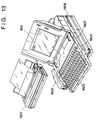
- Fig. 13 is a perspective view of the information processing apparatus in Fig. 12.
- reference numeral 1901 denotes a flat panel display using the above liquid crystal panel, which displays various menus, graphic pattern information, document information, and the like.
- a coordinate input or item designation input operation can be performed on the flat panel display 1901 by pressing the surface of the touch panel 1803 with a finger of the user or the like.
- Reference numeral 1902 denotes a handset used when the apparatus is used as a telephone set.
- a keyboard 1903 is detachably connected to the main body via a cord and is used to perform various document functions and input various data. This keyboard 1903 has various function keys 1904.
- Reference numeral 1905 denotes an insertion port through which a floppy disk is inserted into the external memory unit 1812.
- Reference numeral 1906 denotes an original table on which an original to be read by the image reader unit 1807 is placed. The read original is discharged from the rear portion of the apparatus. In a facsimile receiving operation, received data is printed out by an ink-jet printer 1907.
- the above information processing apparatus When the above information processing apparatus is to serve as a personal computer or a wordprocessor, various kinds of information input through the keyboard unit 1811 are processed by the control unit 1801 in accordance with a predetermined program, and the resultant information is output, as an image, to the printer unit 1806.
- facsimile information input through the transmission/reception unit 1808 via a communication line is subjected to reception processing in the control unit 1801 in accordance with a predetermined program, and the resultant information is output, as a received image, to the printer unit 1806.
- an original is read by the image reader unit 1807, and the read original data is output, as an image to be copied, to the printer unit 1806 via the control unit 1801.
- original data read by the image reader unit 1807 is subjected to transmission processing in the control unit 1801 in accordance with a predetermined program, and the resultant data is transmitted to a communication line via the transmission/reception unit 1808.
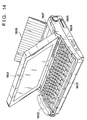
- the above information processing apparatus may be designed as an integrated apparatus incorporating an ink-jet printer in the main body, as shown in Fig. 14. In this case, the portability of the apparatus can be improved.
- the same reference numerals in Fig. 14 denote parts having the same functions as those in Fig. 13.
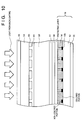
- Fig. 3 shows the structure of an ink-jet head IJH for spraying ink on the layer 14 in the color filter as described above.
- the ink-jet head IJH mainly comprises a heater board 104 as a board on which a plurality of heaters 102 for heating an ink are formed, and a ceiling plate 106 mounted on the heater board 104.
- a plurality of discharging openings 108 are formed in the ceiling plate 106.
- Tunnel-like fluid passages 110 communicating with the discharging openings 108 are formed therebehind.
- the respective fluid passages 110 are isolated from the adjacent fluid passages via partition walls 112.
- the respective fluid passages 110 are commonly connected to one ink chamber 114 at the rear side of the fluid passages.
- An ink is supplied to the ink chamber 114 via an ink inlet 116. This ink is supplied from the ink chamber 114 to each fluid passage 110.
- the heater board 104 and the ceiling plate 106 are positioned such that the position of each heater 102 coincides with that of a corresponding fluid passage 110, and are assembled into the state shown in Fig. 3.
- Fig. 3 shows only two heaters 102, the heater 102 is arranged in correspondence with each fluid passage 110.
- a predetermined driving signal is supplied to the heater 102 in the assembled state shown in Fig. 3, an ink above the heater 102 is boiled to produce a bubble, and the ink is pushed and discharged from the discharging opening 108 upon volume expansion of the ink. Therefore, the size of a bubble can be adjusted by controlling a driving pulse applied to the heater 102, e.g., controlling the magnitude of power. That is, the volume of the ink discharged from each discharging opening can be arbitrarily controlled.
- Fig. 4 is a timing chart for explaining a method of controlling the amount of ink discharged by changing power supplied to each heater in this manner.
- the two pulses are a preheat pulse and a main heat pulse (to be simply referred to as a heat pulse hereinafter).
- the preheat pulse is a pulse for heating an ink to a predetermined temperature before the ink is actually discharged.
- the pulse width of this pulse is set to be smaller than a minimum pulse width t5 required to discharge the ink. Therefore, the ink is not discharged by this preheat pulse.
- the preheat pulse is applied to each heater 102 to increase the initial temperature of the ink to a predetermined temperature in advance so as to always make the amount of ink discharged constant when a constant heat pulse is applied to the heater 102 afterward.
- the temperature of the ink may be adjusted in advance by adjusting the width of a preheat pulse. In this case, for the same heat pulse, the amount of ink discharged can be changed.
- the start time required to discharge the ink upon application of the heat pulse can be shortened to improve the responsibility.
- the heat pulse is a pulse for actually discharging the ink.
- the pulse width of the heat pulse is set to be larger than the minimum pulse width t5 required to discharge the ink.
- Energy generated by each heater 102 is proportional to the width (application time) of a heat pulse. Therefore, variations in the characteristics of the heaters 102 can be adjusted by adjusting the width of each heat pulse.
- the amount of ink discharged can also be adjusted by adjusting the interval between a preheat pulse and a heat pulse to control the dispersed state of heat upon application of the preheat pulse.
- the amount of ink discharged can be controlled both by adjusting the application time of a preheat pulse and by adjusting the interval between application of a preheat pulse and that of a heat pulse. Therefore, by adjusting the application time of a preheat pulse or the interval between application of a preheat pulse and that of a heat pulse as needed, the amount of ink discharged or the responsibility of discharging of the ink with respect to an applied pulse can be arbitrarily adjusted.
- an ink is discharged in different amounts from discharging openings (nozzles) 108a, 108b, and 108c upon application of the same amount of energy, as shown in Fig. 4. More specifically, assume that when a predetermined amount of energy is applied at a predetermined temperature, the amount of ink discharged from the nozzle 108a is 36 pl (pico-liters); the amount of ink discharged from the nozzle 108b, 40 pl; and the amount of ink discharged from the nozzle 108c, 40 pl, and the resistance of heaters 102a and 102b corresponding to the nozzles 108a and 108b is 200 ⁇ , and the resistance of a heater 102c corresponding to the nozzle 108c is 210 ⁇ . Assume that the amounts of ink discharged from the nozzles 108a, 108b, and 108c are to be adjusted to 40 pl.
- the widths of a preheat pulse and a heat pulse may be adjusted to adjust the amounts of ink discharged from the nozzles 108a, 108b, and 108c to the same amount.
- Various combinations of the widths of preheat pulses and heat pulses are conceivable. In this case, the amounts of energy generated by heat pulses are made equal for the three nozzles, and the amounts of ink discharged are adjusted by adjusting the widths of preheat pulses.
- the amounts of energy generated by heat pulses can be made equal by applying voltage pulses having the same width to the heaters 102a and 102b.
- the width of each voltage pulse is set to be t3 which is larger than the width t5.
- An ink is discharged in different amounts, i.e., 36 pl and 40 pl, from the nozzles 108a and 108b upon application of the same amount of energy.
- a preheat pulse having a width t2 larger than a width t1 of a preheat pulse applied to the heater 102b is applied to the heater 102a.
- the amounts of ink discharged from the heaters 108a and 108b can be adjusted to 40 pl.
- the heater 102c for the nozzle 108c has a resistance of 210 ⁇ , which is higher than the resistance of the two remaining heaters 102a and 102b. For this reason, in order to cause the heater 102c to generate the same amount of energy as that generated by the two remaining heaters, the width of a heat pulse must be set to be larger than that of the above heat pulse. In this case, therefore, the width of the heat pulse is set to be t4 which is larger than the width t3. Since the amounts of ink discharged from the nozzles 108b and 108c upon application of a predetermined amount of energy are the same, the width of a preheat pulse required is equal to that of a preheat pulse applied to the heater 102b. That is, a preheat pulse having the width t1 is applied to the heater 102c.
- the same amount of ink can be discharged from the nozzles 108a, 108b, and 108c which discharge an ink in different amounts upon application of a predetermined amount of energy.
- the amounts of ink discharged may be intentionally made to differ from each other.
- Fig. 5 shows the arrangement of an apparatus for manufacturing the color filter shown in Figs. 1A or 1B and 2.
- a manufacturing apparatus 20 comprises an X-Y table 22 mounted on a base (not shown) and capable of moving in the X and Y directions in Fig. 5, and an ink-jet head IJH fixed on a base via a support member (not shown) above the X-Y table 22.
- a glass substrate 12 on which a light-shielding grating 10b and a layer 14 to be colored (see Fig. 2) are formed by the above method is placed on the X-Y table 22.
- the ink-jet head IJH includes a red head 120a for discharging a red ink, a green head 120b for discharging a green ink, and a blue head 120c for discharging a blue ink. These heads 120a, 120b, and 120c are designed to discharge inks independently.
- an R (red), G (green), or B (blue) ink is discharged into a desired frame of the light-shielding grating 10b while the X-Y table 22 moves with respect to the ink-jet head IJH in the X and Y directions. In this manner, each frame of the light-shielding grating 10b is colored to complete a color filter.
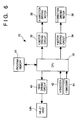
- Fig. 6 is a block diagram showing the arrangement of the manufacturing apparatus 20.
- X- and Y-direction driving motors 36 and 38 for driving the X-Y table 22 in the X and Y directions are connected to a CPU 30 for controlling the overall operation of the manufacturing apparatus 20 via X and Y motor driving circuits 32 and 34.
- the ink-jet head IJH is also connected to the CPU 30 via a head driving circuit 40.
- X and Y encoders 42 and 44 for detecting the position of the X-Y table 22 is connected to the CPU 30. With this arrangement, position information on the X-Y table 22 is input to the CPU 30.
- a control program in a program memory 46 is input to the CPU 30.
- the CPU 30 moves the X-Y table 22 in accordance with this control program and position information from the X and Y encoders 42 and 44. With this operation, a desired grating frame on the glass substrate 12 is brought to a position below the ink-jet head IJH, and an ink having a desired color is discharged into the frame to color it. A color filter is manufactured by performing this operation for each frame of the light-shielding grating 10b.
- Figs. 7 to 9 are sectional views showing the concept of a color filter manufacturing method of this embodiment.
- the light-shielding grating 10b is formed on the glass substrate 12 cleaned by a normal method, as shown in Fig. 7.
- the layer 14 to be colored is formed thereon.
- a material is dissolved or dispersed in a proper solvent to obtain a coating solution.
- the coating solution prepared in this manner is coated by a roller coater method, a blade coater method, an air-knife coater method, a rod bar coater method, a spin coater method, and the like.
- the resultant structure is baked by an oven, a hotplate, or the like to evaporate the solvent, thereby forming a film.
- a thickness (d ⁇ m) of the dry film must satisfy a relation d > Vo/500 with respect to an amount Vo pl (pico-liters) of ink discharged at one discharge (one droplet) from an ink-jet head to be used.
- the light-shielding grating 10b need not be performed on the glass substrate 12.
- the layer 14 to be colored may be formed on the glass substrate 12, and then the light-shielding grating 10b may be formed thereon by photolithography or an ink-jet method.
- the material of the layer 14 to be colored must have ink reception ability, a high dot resolution, and excellent transparency.
- the material of the layer 14 to be colored must have good adhesion properties with the protective film and a process resistance such as heat resistance.
- a preferable example of the material of the layer 14 to be colored is an ink reception layer (layer to be colored) material used for a well-known ink-jet OHP film, but other examples are polyvinyl alcohol, polyvinyl pyrrolidone, a starch, casein, albumin, sodium alginate, gelatin, polyacrylamide, carboxymethyl cellulose, methyl cellulose, hydroxyethyl cellulose, hydroxypropyl cellulose, polyvinyl acetate, polyacrylic acid, and derivatives of these examples.
- the material of the layer 14 to be colored is not limited to them, as a matter of course. Of these examples, hydroxypropyl cellulose and a derivative thereof are preferably used from the viewpoint of the process resistance such as heat resistance.
- these examples are excellent in adhesion properties and heat resistance, and can be easily used in a manufacturing process. From the viewpoint of the transparency and the ink reception ability, these examples are preferably used as the layer to be colored of a color filter. In addition, these examples have a high dot resolution. For this reason, if the conditions of the present invention are satisfied, i.e., the thickness (d ⁇ m) of a dry film satisfies the relation d > Vo/500 with respect to the amount Vo (pl: pico-liter) of ink discharged at one discharge (one droplet) from the ink-jet head to be used, inks of three different colors (red, green, and blue) will not mix with each other in the layer 14 to be colored.
- a crosslinking agent such as methylol melamine, methylol hydroxypropylene urea, dimethylol urea, and isocyanate, which is not limited to them, may be mixed in the material of a layer to be colored.
- the resultant structure may be heated or set by light irradiation.
- Preferable examples of the material of the layer 14 to be colored are acrylic-based polymers containing a crosslinkable monomer unit, such as N-methylolacrylamide, which can improve the process resistance.
- a crosslinkable monomer unit such as N-methylolacrylamide
- a suitable color filter can be formed if the above relation d > Vo/500 is established when the thickness of the material of the layer 14 to be colored is d ( ⁇ m) and the amount of ink discharged is Vo (pl: pico-liter).
- the ink permeability of the layer 14 to be colored its penetration degree and speed are not particularly limited as long as the layer 14 to be colored can absorb an ink to be used. It is enough for the layer 14 to be colored to have almost the same penetration degree and speed as those of a general material to be recorded for an ink-jet printer. More specifically, when a 50-pl ink is discharged to a layer to be colored having a thickness of 1 ⁇ m, a time required for the ink to penetrate the layer to be colored is preferably about 5 minutes to 1 hour at most. According to the embodiment, the layer 14 to be colored has an absorbency of which an ink no longer exists as fluid on the surface of the layer one hour after the ink is discharged.
- the surface of the layer 14 As a means of determining, it is suggested to view the surface of the layer 14 to be colored with a microscope. By viewing the surface of the layer with a microscope, it can be determined whether or not the ink still exists as fluid on the surface of the layer, for instance, whether the ink flows out of the substrate when the glass substrate 12 is tilted.
- the number of ink droplets discharged to one film element is preferably 1 to 7 when the volume of one droplet is assumed to be 40 pl.
- one filter element is colored by a plurality of ink droplets
- the droplets can be discharged and overlaid on a same spot or can be discharged on a different spot by shifting the spot little by little.
- R (red), G (green), and B (blue) inks are discharged to the layer 14 to be colored which is formed in the above manner in accordance with the pattern of the light-shielding grating 10b by the ink-jet method.
- both the pattern of the light-shielding grating 10b and the pattern of R, G, and B may be formed by discharging the inks by the ink-jet system.
- the volume of each ink dot at this time is Vo (pl: pico-liter), as described above.
- the ink-jet system comprises a system using heat energy and a system using mechanical energy, either of which can be suitably used.
- An ink is not particularly limited as long as it can be used for the ink-jet system.
- the dyes or pigments of R, G, and B may be selected in accordance with application purposes. Any solvent composition can be used as long as it can be used for the ink-jet system, and a composition is not particularly limited.
- a dye and a pigment can be suitably used as coloring materials.
- the above relation is hardly affected by the kind of coloring material, but depends on an ink solvent.
- an ink solvent to be used are water generally used as an ink-jet ink, and a water-soluble organic solvent used by being mixed with water.
- the water-soluble organic solvent are alkyl alcohols having 1 to 4 carbon atoms (e.g., methyl alcohol, ethyl alcohol, n-propyl alcohol, isopropyl alcohol, n-butyl alcohol, sec-butyl alcohol, and tert-butyl alcohol), amides (e.g., dimethylformamide and dimethylacetamide), ketones or ketoalcohols (e.g., acetone and diacetone alcohol), ethers (e.g., tetrahydrofuran and dioxane), polyalkylene glycols (e.g., polyethylene glycol and polypropylene glycol), alkylene glycols containing an alkylene group having 2 to 6 carbon atoms (e.g., ethylene glycol, propylene glycol, butylene glycol,
- alkyl alcohols containing an alkylene group having 2 to 6 carbon atoms e.g., ethylene glycol, propylene glycol, butylene glycol, triethylene glycol, 1,2,6-hexanetriol, thiodiglycol, hexylene glycol, and diethylene glycol
- an additive such as a surfactant may be added to the ink.
- a protective film 15 is coated on the layer 14 to be colored to which the ink is discharged by the ink-jet system. This arrangement can greatly improve the process resistance, and particularly resistance to solvents. If the layer 14 to be colored itself has a sufficient process resistance, the protective film 15 can be eliminated, but generally formed.
- a coating method may be the same as that of coating the layer to be colored.
- the material of the protective film 15 is not particularly limited as long as it is a protective film material used for a general color filter. An acrylic or epoxy thermosetting/photosetting material can be suitably used.
- the coated substrate is baked by an oven, a hotplate, or the like to form a film.
- the thickness of this protective film which is determined by required properties and the like, is about 0.1 to 10 ⁇ m.
- the color filter formed by the above ink-jet method the number of steps is greatly decreased.
- the color filter can be manufactured at a reduced material cost. It has satisfactory process resistances such as heat resistance and resistance to solvents, and also satisfactory ink reception ability and dot resolution. Therefore, the color filter performance is very high as a color liquid crystal display free from ink blurring, color mixing, and white omissions.
- thermosetting resin composition consisting of a mixture of hydroxypropyl cellulose (HPC-H available from Nihon Soda) and dimethylol hydroxyethylene urea (Sumitex resin NS-11 available from Sumitomo Kasei) was spin-coated on a glass substrate on which a light-shielding grating was formed so as to have a dry film thickness of 0.6 ⁇ m.
- the resultant structure was pre-baked at 110°C for 10 minutes.
- This structure served as a layer to be colored.
- the layer to be colored was colored in the matrix pattern of R, G, and B with pigment inks. The amount of ink discharged of each color was 40 pl at that time.
- a liquid crystal color filter was formed in the same manner as in Example 1 except for a thermosetting resin composition consisting of a mixture of hydroxyethyl cellulose (AH-15 available from Fuji Chemical) and methylated methylolmelamine (M-6 available from Sumitomo Kasei).
- a thermosetting resin composition consisting of a mixture of hydroxyethyl cellulose (AH-15 available from Fuji Chemical) and methylated methylolmelamine (M-6 available from Sumitomo Kasei).
- a liquid crystal color filter was formed in the same manner as in Example 1 except that an ink was a dye ink.
- This structure served as a layer to be colored.
- the layer to be colored was colored in the matrix pattern of R, G, and B with pigment inks. The amount of ink discharged of each color was 50 pl at that time.
- a liquid crystal color filter was formed in the same manner as in Example 4 except that an ink was a dye ink.
- liquid crystal color filters formed in Examples 1 to 5 were observed with an optical microscope. Any faults such as discoloration, mixing of R, G, and B colors, color nonuniformity, ink blurring, and white omissions were not observed.
- a series of operations e.g., formation of ITO and aligning films and sealing of a liquid crystal material, were performed by using the obtained color filter, thereby forming a color-liquid crystal driving apparatus.
- the manufactured color liquid crystal driving apparatus was driven within a temperature range of 0°C to 40°C continuously for 1,000 hours, no failure occurred. Further, when this color liquid crystal driving apparatus was set on an OHP and driven to perform a reflection operation continuously for 1,000 hours, no change in transmittance and color tone was confirmed.
- a liquid crystal color filter was formed in the same manner as in Example 1 except that a resin composition for a layer to be colored was coated to have a dry film thickness of 0.05 ⁇ m.
- a liquid crystal color filter was formed in the same manner as in Example 4 except that a resin composition for a layer to be colored was coated to have a dry film thickness of 0.08 ⁇ m.
- the liquid crystal color filters formed in Comparative Examples 1 and 2 were observed with an optical microscope. No discoloration occurred but faults of color nonuniformity and color mixing were observed.
- the thickness of the layer to be colored is to be d ( ⁇ m), and that the volume of a droplet is to be Vo pl (pico-liters). If d > Vo/500, preferably d > Vo/200, and more preferably d > Vo/100 are established, ink blurring which may occur in a very thin layer to be colored is prevented to prevent color mixing between adjacent filter elements, and the like. Therefore, a color filter can be manufactured without causing any ink blurring and any color mixing.
- the ink-jet head is fixed, and the X-Y stage is moved.
- the ink-jet head may be moved while the stage is fixed.
- a so-called piezoelectric type head using mechanical energy converters such as piezoelectric elements may be used as the ink-jet head.
- the volume of the ink discharged can be easily adjusted by adjusting the applied voltage of a driving pulse.
- the ink volume can be adjusted by adjusting both or either of bipolar driving pulses.
- the present invention can be applied to a single-color filter and a filter of a type having a plurality of single-color filters of different colors stacked on each other.
- the present invention is applied to the print apparatus of the system, among various ink-jet recording systems, which has a means (e.g., an electricity-to-heat converter or laser light) for generating heat energy as energy used to discharge an ink, and changes the state of an ink by using the heat energy.
- a means e.g., an electricity-to-heat converter or laser light
- heat energy as energy used to discharge an ink
- changes the state of an ink by using the heat energy e.g., a high-density, high-definition recording operation can be realized.
- the on-demand type apparatus is employed because of the structure arranged in such a manner that one or more drive signals, which rapidly raise the temperature of an electricity-to-heat converter disposed to face a sheet or a fluid passage which holds the fluid (ink) to a level higher than levels at which film boiling takes place are applied to the electricity-to-heat converter in accordance with recording information so as to generate heat energy in the electricity-to-heat converter and to cause the heat effecting surface of the recording head to take place film boiling so that bubbles can be formed in the fluid (ink) to correspond to the one or more drive signals.
- one or more drive signals which rapidly raise the temperature of an electricity-to-heat converter disposed to face a sheet or a fluid passage which holds the fluid (ink) to a level higher than levels at which film boiling takes place are applied to the electricity-to-heat converter in accordance with recording information so as to generate heat energy in the electricity-to-heat converter and to cause the heat effecting surface of the recording head to take place film boiling so that bubbles can be formed in
- the enlargement/contraction of the bubble will cause the fluid (ink) to be discharged through a discharging opening so that one or more droplets are formed. If a pulse shape drive signal is employed, the bubble can be enlarged/contracted immediately and properly, causing a further preferred effect to be obtained because the fluid (ink) can be discharged while revealing excellent responsibility.
- a structure having an arrangement that the heat effecting surface is disposed in a bent region and disclosed in U.S. Patent No. 4,558,333 or 4,459,600 may be employed.
- the following structures may be employed: a structure having an arrangement that a common slit is formed to serve as a discharge section of a plurality of electricity-to-heat converters and disclosed in Japanese Patent Laid-Open No. 59-123670; and a structure disclosed in Japanese Patent Laid-Open No. 59-138461 in which an opening for absorbing pressure waves of heat energy is disposed to correspond to the discharge section.
- a recording head of the full line type having a length corresponding to the maximum width of a recording medium which can be recorded by the recording apparatus
- either the construction which satisfies its length by a combination of a plurality of recording heads as disclosed in the above specifications or the construction as a single full line type recording head which has integrally been formed can be used.
- the invention is effective for a recording head of the freely exchangeable chip type which enables electrical connection to the recording apparatus main body or supply of ink from the main device by being mounted onto the apparatus main body, or for the case by use of a recording head of the cartridge type provided integrally on the recording head itself.
- the recording head restoring means and the auxiliary means provided as the component of the present invention because the effect of the present invention can be further stabled.
- a recording head capping means a cleaning means, a pressurizing or suction means, an electricity-to-heat converter, an another heating element or a sub-heating means constituted by combining them and a sub-emitting mode in which an emitting is performed independently from the recording emitting in order to stably perform the recording operation.
- a fluid ink is employed in the aforesaid embodiment of the present invention
- an ink which is solidified at the room temperature or lower and as well as softened at the room temperature an ink in the form of a fluid at the room temperature, or an ink which is formed into a fluid when the recording signal is supplied may be employed because the aforesaid ink-jet method is ordinarily arranged in such a manner that the temperature of ink is controlled in a range from 30°C or higher to 70°C or lower so as to make the viscosity of the ink to be included in a stable discharge range.
- an ink which is solidified when it is caused to stand, and liquified when heat energy is supplied in accordance with a recording signal can be adapted to the present invention to positively prevent a temperature rise caused by heat energy by utilizing the temperature rise as energy of state transition from the solid state to the liquid state or to prevent ink evaporation.
- an ink which is liquified when heat energy is supplied in accordance with a recording signal so as to be discharged in the form of fluid ink, or an ink which is liquified only after heat energy is supplied, e.g., an ink which starts to solidify when it reaches a recording medium, can be adapted to the present invention.
- the ink may be of a type which is held as fluid or solid material in a recess of a porous sheet or a through hole at a position to face the electricity-to-heat converter as disclosed in Japanese Patent Laid-Open No. 54-56847 or Japanese Patent Laid-Open No. 60-71260. It is the most preferred way for the ink to be adapted to the aforesaid film boiling method.
- the thickness of the layer to be colored is to be d( ⁇ m), and that the volume of a droplet is to be Vo (pl: pico-liters). If d > Vo/500 is established, ink blurring which occurs in a very thin layer to be colored is prevented to prevent color mixing between adjacent filter elements, and the like. Therefore, a color filter can be manufactured without causing any ink blurring and any color mixing.
- droplets are discharged by using the ink-jet head.
- a color filter having filter elements in a plurality of colors can be manufactured by one step, achieving a reduction in cost of the color filter.
Abstract
Description
- The present invention relates to a method of manufacturing a color filter by forming and arranging a plurality of colored filter elements on a transparent substrate, the color filter, a liquid crystal display apparatus, and an apparatus having the liquid crystal display apparatus.
- With recent advances in personal computers, especially portable personal computers, the demand tends to arise for liquid crystal displays, especially color liquid crystal displays. However, in order to further popularize the use of liquid crystal displays, a reduction in cost must be achieved. Especially, it is required to reduce the cost of a color filter which occupies a large proportion of the total cost. Various methods have been tried to satisfy the required characteristics of color filters while meeting the above requirements. However, any method capable of satisfying all the requirements has not been established. The respective methods will be described below. The first method is a coloring method, which is the most popular method. In the coloring method, a water-soluble polymer material as a colorable material is coated on a glass substrate, and the coating is patterned into a desired shape by a photolithography process. The obtained pattern is dipped in a color bath to obtain a colored pattern. This process is repeated three times to form R, G, and B color filter layers.
- The second method is a pigment dispersion method, which is currently replacing the coloring method. In this method, a pigment-dispersed photosensitive resin layer is formed on a substrate and patterned into a single-color pattern. This process is repeated three times to obtain R, G, and B color filter layers.
- The third method is an electrodeposition method. In this method, a transparent electrode is patterned on a substrate, and the resultant structure is dipped in an electrodeposition coating fluid containing a pigment, a resin, an electrolyte, and the like to be colored in the first color by electrodeposition. This process is repeated three times to form R, G, and B color filter layers. Finally, these layers are calcined.
- The fourth method is a method of dispersing a pigment in a thermosetting resin, performing a print operation three times to form R, G, and B coatings separately, and thermosetting the resins, thereby forming colored layers. In either of the above methods, a protective layer is generally formed on the colored layers.
- The point common to these methods is that the same process must be repeated three times to obtain layers colored in three colors, i.e., R, G, and B. This causes an increase in cost. In addition, as the number of processes increases, the yield decreases. In the electrodeposition method, limitations are imposed on pattern shapes which can be formed. For this reason, with the existing techniques, this method cannot be applied to TFTs. In the print method, a pattern with a fine pitch cannot be formed because of poor resolution and poor evenness.
- In order to eliminate these drawbacks, methods of manufacturing color filters by an ink-jet system are disclosed in Japanese Patent Laid-Open Nos. 59-75205, 63-235901, 1-217320, and 4-123005.
- The above manufacturing methods by the conventional ink-jet system cannot manufacture a satisfactory color filter in view of ink blurring, color mixing between adjacent filter elements, white omissions, and the like.
- The present invention has been made in consideration of the above situation, and has as its object to provide a color filter manufacturing method which can manufacture a low-cost color filter without causing any ink blurring, any color mixing, and any color omission.
- It is another object of the present invention to provide a color filter manufactured by the above manufacturing method, a liquid crystal display apparatus, and an apparatus having this liquid crystal display apparatus.
- In order to solve the above problems and achieve the above objects, a color filter manufacturing method of the present invention is characterized by the following arrangement.
- That is, there is provided a manufacturing method for a color filter formed by forming a layer to be colored on a transparent substrate, and discharging an ink colored in a predetermined color to the layer for coloring the layer, wherein when a thickness of the layer to be colored is assumed to be d (µm) and a volume of the ink discharged at one discharge is to be Vo (pl: pico-liter), the thickness of the layer to be colored and the volume of the ink are adjusted to establish d > Vo/500.
- A color filter of the present invention is characterized by the following arrangement.
- That is, there is provided a color filter formed by forming a layer to be colored on a transparent substrate, and discharging an ink colored in a predetermined color to the layer for coloring the layer, wherein when a thickness of the layer to be colored is assumed to be d (µm) and a volume of the ink discharged at one discharge is to be Vo (pl: pico-liter), the color filter is manufactured by adjusting the thickness of the layer to be colored and the volume of the ink so as to establish d > Vo/500.
- A liquid crystal display apparatus of the present invention is characterized by the following arrangement.
- That is, there is provided a liquid crystal display apparatus using a color filter formed by forming a layer to be colored on a transparent substrate, and discharging an ink colored in a predetermined color to the layer for coloring the layer, comprising: a color filter manufactured by adjusting a thickness of the layer to be colored and a volume of the ink to establish d > Vo/500 when the thickness of the layer to be colored is assumed to be d (µm) and the volume of the ink discharged at one discharge is to be Vo (pl: pico-liter); and a substrate opposing the color filer, wherein a liquid crystal compound is sealed between the substrates.
- An apparatus having a liquid crystal display apparatus of the present invention is characterized by the following arrangement.
- That is, there is provided an apparatus having a liquid crystal display apparatus using a color filter formed by forming a layer to be colored on a transparent substrate, and discharging an ink colored in a predetermined color to the layer for coloring the layer, comprising: a liquid crystal display apparatus having a color filter manufactured by adjusting a thickness of the layer to be colored and a volume of the ink to establish d > Vo/500 when the thickness of the layer to be colored is assumed to be d (µm) and the volume of the ink discharged at one discharge is to be Vo (pl: pico-liter), and a substrate opposing the color filer, wherein a liquid crystal compound is sealed between the substrates; and image signal output means for outputting an image signal to the liquid crystal display apparatus.
- Other objects and advantages besides those discussed above shall be apparent to those skilled in the art from the description of a preferred embodiment of the invention which follows. In the description, reference is made to accompanying drawings, which form a part thereof, and which illustrate an example of the invention. Such example, however, is not exhaustive of the various embodiments of the invention, and therefore reference is made to the claims which follow the description for determining the scope of the invention.
-
- Figs. 1A and 1B are partial enlarged views showing color filters manufactured by a manufacturing method and apparatus according to the present invention;
- Fig. 2 is a side sectional view showing the color filter in Fig. 1A or 1B;
- Fig. 3 is a view showing the structure of an ink-jet head IJH for spraying an ink on a layer to be colored;
- Fig. 4 is a timing chart for explaining a method of controlling the amount of ink discharged by changing power supplied to a heater;
- Fig. 5 is a perspective view showing the arrangement of an apparatus for manufacturing the color filter shown in Figs. 1A or 1B and 2;
- Fig. 6 is a block diagram showing the arrangement of the color filter manufacturing apparatus;
- Fig. 7 is a sectional view showing a method of manufacturing a liquid crystal color filter;
- Fig. 8 is a sectional view showing the method of manufacturing the liquid crystal color filter;
- Fig. 9 is a sectional view showing the method of manufacturing the liquid crystal color filter;
- Fig. 10 is a side sectional view showing the structure of a color liquid crystal panel;
- Fig. 11 is a side sectional view showing the structure of a color liquid crystal panel;
- Fig. 12 is a block diagram showing an information processing apparatus using a liquid crystal panel;
- Fig. 13 is a perspective view showing an information processing apparatus using a liquid crystal panel; and
- Fig. 14 is a perspective view showing an information processing apparatus using a liquid crystal panel.
- The preferred embodiment of the present invention will be described in detail below with reference to the accompanying drawings.
- Figs. 1A and 1B are partial enlarged views of color filters manufactured by a manufacturing method according to the present invention.
- Each
color filter 10 is mounted on the front surface of a color liquid crystal display or the like used for a portable personal computer or the like. As shown in Figs. 1A and 1B,filter elements 10a colored in R (red), G (green), and B (blue) are two-dimensionally arranged in a matrix form. In the color filter shown in Fig. 1A, thefilter elements 10a are arranged in a simple matrix form. In the color filter shown in Fig. 1B, thefilter elements 10a are arranged in a staggered form. A black light-shielding grating 10b is formed between therespective filter elements 10a to make the boundaries between thefilter elements 10a clear so as to provide a clear screen. Note that according to the embodiment, each filter element is formed in a rectangular shape having shorter sides of 50 to 100 µm and longer sides of 150 to 450 µm. - Fig. 2 is a side sectional view of the
color filter 10 in Fig. 1A or 1B. The light-shielding grating 10b is formed on aglass substrate 12 constituting the main body of thecolor filter 10. Thefilter elements 10a of the respective colors are formed on the light-shielding grating 10b. - In manufacturing the
color filter 10, chromium is deposited on theglass substrate 12 by sputtering, and the resultant film is formed into a matrix pattern by photolithography. This pattern is the light-shielding grating 10b. Alayer 14 to be colored is formed on the light-shielding grating 10b. Thelayer 14 consists of a cellulose, an acrylic resin, gelatin, or the like and absorbs a fluid. Droplets (to be referred to as an ink hereinafter) containing a coloring material (dye) are sprayed on the filter element formation regions of thelayer 14 by a recording head of the ink-jet system. With this process, thelayer 14 is colored to form thecolor filter elements 10a. - In general, a color liquid crystal panel is formed by joining the
color filter substrate 12 to acounter substrate 54 and sealing aliquid crystal compound 52 therebetween. TFTs (Thin Film Transistors; not shown) andtransparent pixel electrodes 53 are formed on the inner surface of onesubstrate 54 of the liquid crystal panel in a matrix form. Thecolor filter 10 is placed on the inner surface of theother substrate 12 such that the R, G, and B coloring materials are positioned to oppose the pixel electrodes. A transparent counter electrode (common electrode) 50 is formed on the entire surface of thecolor filter 10. The light-shielding grating 10b is generally formed on thecolor filter substrate 12 side (see Fig. 10). However, in a BM (black matrix) on-array type liquid crystal panel, such a grating is formed on the TFT substrate side opposing the color filter substrate (see Fig. 11). Aligningfilms 51 are formed within the planes of the two substrates. By performing a rubbing process for the aligningfilms 51, the liquid crystal molecules can be aligned in a predetermined direction. Polarizingplates 55 are bonded to the outer surface of the respective glass substrates. Theliquid crystal compound 52 is filled in the gap (about 2 to 5 µm) between these glass substrates. As a blacklight, a combination of a fluorescent lamp (not shown) and a scattering plate (not shown) is generally used. A display operation is performed by causing the liquid crystal compound to serve as an optical shutter for changing the transmittance for light emitted from the backlight. - A case wherein the above liquid crystal panel is applied to an information processing apparatus will be described below with reference to Figs. 12 to 14.
- Fig. 12 is a block diagram showing the schematic arrangement of an information processing apparatus serving as a wordprocessor, a personal computer, a facsimile apparatus, and a copying machine, to which the above liquid crystal panel is applied.
- Referring to Fig. 12,
reference numeral 1801 denotes a control unit for controlling the overall apparatus. Thecontrol unit 1801 includes a CPU such as a microprocessor and various I/O ports, and performs control by outputting/inputting control signals, data signals, and the like to/from the respective units.Reference numeral 1802 denotes a display unit for displaying various menus, document information, and image data read by animage reader 1807, and the like on the display screen; 1803, a transparent, pressure-sensitive touch panel mounted on thedisplay unit 1802. By pressing the surface of thetouch panel 1803 with a finger of the user or the like, an item input operation, a coordinate position input operation, or the like can be performed on thedisplay unit 1802. -
Reference numeral 1804 denotes an FM (Frequency Modulation) sound source unit for storing music information, created by a music editor or the like, in amemory unit 1810 or anexternal memory unit 1812 as digital data, and reading out the information from such a memory, thereby performing FM modulation of the information. An electrical signal from the FMsound source unit 1804 is converted into an audible sound by aspeaker unit 1805. Aprinter unit 1806 is used as an output terminal for the wordprocessor, the personal computer, the facsimile apparatus, and the copying machine. -
Reference numeral 1807 denotes an image reader unit for photoelectrically reading original data. Theimage reader unit 1807 is arranged midway along the original convey passage and designed to read originals for facsimile and copy operations and other various originals. -
Reference numeral 1808 denotes a transmission/reception unit for the facsimile (FAX) apparatus. The transmission/reception unit 1808 transmits original data read by theimage reader unit 1807 by facsimile, and receives and decodes a sent facsimile signal. The transmission/reception unit 1808 has an interface function for external units.Reference numeral 1809 denotes a telephone unit having a general telephone function and various telephone functions such as an answering function. -
Reference numeral 1810 denotes a memory unit including a ROM for storing system programs, manager programs, application programs, fonts, and dictionaries, a RAM for storing an application program loaded from theexternal memory unit 1812 and document information, a video RAM, and the like. -
Reference numeral 1811 denotes a keyboard unit for inputting document information and various commands. -
Reference numeral 1812 denotes an external memory unit using a floppy disk, a hard disk, and the like as a memory medium. Theexternal memory unit 1812 serves to store document information, music and speech information, application programs of the user, and the like. - Fig. 13 is a perspective view of the information processing apparatus in Fig. 12.
- Referring to Fig. 13,
reference numeral 1901 denotes a flat panel display using the above liquid crystal panel, which displays various menus, graphic pattern information, document information, and the like. A coordinate input or item designation input operation can be performed on theflat panel display 1901 by pressing the surface of thetouch panel 1803 with a finger of the user or the like.Reference numeral 1902 denotes a handset used when the apparatus is used as a telephone set. Akeyboard 1903 is detachably connected to the main body via a cord and is used to perform various document functions and input various data. Thiskeyboard 1903 hasvarious function keys 1904.Reference numeral 1905 denotes an insertion port through which a floppy disk is inserted into theexternal memory unit 1812. -
Reference numeral 1906 denotes an original table on which an original to be read by theimage reader unit 1807 is placed. The read original is discharged from the rear portion of the apparatus. In a facsimile receiving operation, received data is printed out by an ink-jet printer 1907. - When the above information processing apparatus is to serve as a personal computer or a wordprocessor, various kinds of information input through the
keyboard unit 1811 are processed by thecontrol unit 1801 in accordance with a predetermined program, and the resultant information is output, as an image, to theprinter unit 1806. - When the information processing apparatus is to serve as the receiver of the facsimile apparatus, facsimile information input through the transmission/
reception unit 1808 via a communication line is subjected to reception processing in thecontrol unit 1801 in accordance with a predetermined program, and the resultant information is output, as a received image, to theprinter unit 1806. - When the information processing apparatus is to serve as the copying machine, an original is read by the
image reader unit 1807, and the read original data is output, as an image to be copied, to theprinter unit 1806 via thecontrol unit 1801. Note that when the information processing apparatus is to serve as the receiver of the facsimile apparatus, original data read by theimage reader unit 1807 is subjected to transmission processing in thecontrol unit 1801 in accordance with a predetermined program, and the resultant data is transmitted to a communication line via the transmission/reception unit 1808. - Note that the above information processing apparatus may be designed as an integrated apparatus incorporating an ink-jet printer in the main body, as shown in Fig. 14. In this case, the portability of the apparatus can be improved. The same reference numerals in Fig. 14 denote parts having the same functions as those in Fig. 13.
- Fig. 3 shows the structure of an ink-jet head IJH for spraying ink on the
layer 14 in the color filter as described above. - Referring to Fig. 3, the ink-jet head IJH mainly comprises a
heater board 104 as a board on which a plurality ofheaters 102 for heating an ink are formed, and aceiling plate 106 mounted on theheater board 104. A plurality of dischargingopenings 108 are formed in theceiling plate 106. Tunnel-likefluid passages 110 communicating with the dischargingopenings 108 are formed therebehind. The respectivefluid passages 110 are isolated from the adjacent fluid passages viapartition walls 112. The respectivefluid passages 110 are commonly connected to oneink chamber 114 at the rear side of the fluid passages. An ink is supplied to theink chamber 114 via anink inlet 116. This ink is supplied from theink chamber 114 to eachfluid passage 110. - The
heater board 104 and theceiling plate 106 are positioned such that the position of eachheater 102 coincides with that of acorresponding fluid passage 110, and are assembled into the state shown in Fig. 3. Although Fig. 3 shows only twoheaters 102, theheater 102 is arranged in correspondence with eachfluid passage 110. When a predetermined driving signal is supplied to theheater 102 in the assembled state shown in Fig. 3, an ink above theheater 102 is boiled to produce a bubble, and the ink is pushed and discharged from the dischargingopening 108 upon volume expansion of the ink. Therefore, the size of a bubble can be adjusted by controlling a driving pulse applied to theheater 102, e.g., controlling the magnitude of power. That is, the volume of the ink discharged from each discharging opening can be arbitrarily controlled. - Fig. 4 is a timing chart for explaining a method of controlling the amount of ink discharged by changing power supplied to each heater in this manner.
- In this embodiment, two types of constant-voltage pulses are applied to each
heater 102 to adjust the amount of ink discharged. The two pulses are a preheat pulse and a main heat pulse (to be simply referred to as a heat pulse hereinafter). The preheat pulse is a pulse for heating an ink to a predetermined temperature before the ink is actually discharged. The pulse width of this pulse is set to be smaller than a minimum pulse width t5 required to discharge the ink. Therefore, the ink is not discharged by this preheat pulse. The preheat pulse is applied to eachheater 102 to increase the initial temperature of the ink to a predetermined temperature in advance so as to always make the amount of ink discharged constant when a constant heat pulse is applied to theheater 102 afterward. In contrast to this, the temperature of the ink may be adjusted in advance by adjusting the width of a preheat pulse. In this case, for the same heat pulse, the amount of ink discharged can be changed. In addition, by heating ink before application of a heat pulse, the start time required to discharge the ink upon application of the heat pulse can be shortened to improve the responsibility. - The heat pulse is a pulse for actually discharging the ink. The pulse width of the heat pulse is set to be larger than the minimum pulse width t5 required to discharge the ink. Energy generated by each
heater 102 is proportional to the width (application time) of a heat pulse. Therefore, variations in the characteristics of theheaters 102 can be adjusted by adjusting the width of each heat pulse. - Note that the amount of ink discharged can also be adjusted by adjusting the interval between a preheat pulse and a heat pulse to control the dispersed state of heat upon application of the preheat pulse.
- As is apparent from the above description, the amount of ink discharged can be controlled both by adjusting the application time of a preheat pulse and by adjusting the interval between application of a preheat pulse and that of a heat pulse. Therefore, by adjusting the application time of a preheat pulse or the interval between application of a preheat pulse and that of a heat pulse as needed, the amount of ink discharged or the responsibility of discharging of the ink with respect to an applied pulse can be arbitrarily adjusted.
- Such adjustment of the amount of ink discharged will be described in detail next.
- Assume that an ink is discharged in different amounts from discharging openings (nozzles) 108a, 108b, and 108c upon application of the same amount of energy, as shown in Fig. 4. More specifically, assume that when a predetermined amount of energy is applied at a predetermined temperature, the amount of ink discharged from the
nozzle 108a is 36 pl (pico-liters); the amount of ink discharged from thenozzle nozzle heaters nozzles heater 102c corresponding to thenozzle 108c is 210 Ω. Assume that the amounts of ink discharged from thenozzles - The widths of a preheat pulse and a heat pulse may be adjusted to adjust the amounts of ink discharged from the
nozzles - Since the
heaters nozzles heaters nozzles nozzle 108a, a preheat pulse having a width t2 larger than a width t1 of a preheat pulse applied to theheater 102b is applied to theheater 102a. With this operation, the amounts of ink discharged from theheaters - The
heater 102c for thenozzle 108c has a resistance of 210 Ω, which is higher than the resistance of the two remainingheaters heater 102c to generate the same amount of energy as that generated by the two remaining heaters, the width of a heat pulse must be set to be larger than that of the above heat pulse. In this case, therefore, the width of the heat pulse is set to be t4 which is larger than the width t3. Since the amounts of ink discharged from thenozzles heater 102b. That is, a preheat pulse having the width t1 is applied to theheater 102c. - In the above manner, the same amount of ink can be discharged from the
nozzles - Fig. 5 shows the arrangement of an apparatus for manufacturing the color filter shown in Figs. 1A or 1B and 2.
- Referring to Fig. 5, a
manufacturing apparatus 20 comprises an X-Y table 22 mounted on a base (not shown) and capable of moving in the X and Y directions in Fig. 5, and an ink-jet head IJH fixed on a base via a support member (not shown) above the X-Y table 22. Aglass substrate 12 on which a light-shielding grating 10b and alayer 14 to be colored (see Fig. 2) are formed by the above method is placed on the X-Y table 22. The ink-jet head IJH includes ared head 120a for discharging a red ink, agreen head 120b for discharging a green ink, and a blue head 120c for discharging a blue ink. Theseheads - In the
manufacturing apparatus 20 having the above arrangement, an R (red), G (green), or B (blue) ink is discharged into a desired frame of the light-shielding grating 10b while the X-Y table 22 moves with respect to the ink-jet head IJH in the X and Y directions. In this manner, each frame of the light-shielding grating 10b is colored to complete a color filter. - Fig. 6 is a block diagram showing the arrangement of the
manufacturing apparatus 20. - Referring to Fig. 6, X- and Y-
direction driving motors CPU 30 for controlling the overall operation of themanufacturing apparatus 20 via X and Ymotor driving circuits CPU 30 via ahead driving circuit 40. Furthermore, X andY encoders CPU 30. With this arrangement, position information on the X-Y table 22 is input to theCPU 30. In addition, a control program in aprogram memory 46 is input to theCPU 30. TheCPU 30 moves the X-Y table 22 in accordance with this control program and position information from the X andY encoders glass substrate 12 is brought to a position below the ink-jet head IJH, and an ink having a desired color is discharged into the frame to color it. A color filter is manufactured by performing this operation for each frame of the light-shielding grating 10b. - Figs. 7 to 9 are sectional views showing the concept of a color filter manufacturing method of this embodiment.
- By the above method, the light-shielding grating 10b is formed on the
glass substrate 12 cleaned by a normal method, as shown in Fig. 7. Thelayer 14 to be colored is formed thereon. As a method of forming thelayer 14 to be colored, a material is dissolved or dispersed in a proper solvent to obtain a coating solution. The coating solution prepared in this manner is coated by a roller coater method, a blade coater method, an air-knife coater method, a rod bar coater method, a spin coater method, and the like. The resultant structure is baked by an oven, a hotplate, or the like to evaporate the solvent, thereby forming a film. At this time, a thickness (d µm) of the dry film must satisfy a relation d > Vo/500 with respect to an amount Vo pl (pico-liters) of ink discharged at one discharge (one droplet) from an ink-jet head to be used. - The light-shielding grating 10b need not be performed on the
glass substrate 12. As is well known, thelayer 14 to be colored may be formed on theglass substrate 12, and then the light-shielding grating 10b may be formed thereon by photolithography or an ink-jet method. - The material of the
layer 14 to be colored must have ink reception ability, a high dot resolution, and excellent transparency. In addition, when a transparent substrate or a protective film is to be used, the material of thelayer 14 to be colored must have good adhesion properties with the protective film and a process resistance such as heat resistance. - A preferable example of the material of the
layer 14 to be colored is an ink reception layer (layer to be colored) material used for a well-known ink-jet OHP film, but other examples are polyvinyl alcohol, polyvinyl pyrrolidone, a starch, casein, albumin, sodium alginate, gelatin, polyacrylamide, carboxymethyl cellulose, methyl cellulose, hydroxyethyl cellulose, hydroxypropyl cellulose, polyvinyl acetate, polyacrylic acid, and derivatives of these examples. The material of thelayer 14 to be colored is not limited to them, as a matter of course. Of these examples, hydroxypropyl cellulose and a derivative thereof are preferably used from the viewpoint of the process resistance such as heat resistance. These examples are excellent in adhesion properties and heat resistance, and can be easily used in a manufacturing process. From the viewpoint of the transparency and the ink reception ability, these examples are preferably used as the layer to be colored of a color filter. In addition, these examples have a high dot resolution. For this reason, if the conditions of the present invention are satisfied, i.e., the thickness (d µm) of a dry film satisfies the relation d > Vo/500 with respect to the amount Vo (pl: pico-liter) of ink discharged at one discharge (one droplet) from the ink-jet head to be used, inks of three different colors (red, green, and blue) will not mix with each other in thelayer 14 to be colored. - In order to improve the process resistance, a crosslinking agent such as methylol melamine, methylol hydroxypropylene urea, dimethylol urea, and isocyanate, which is not limited to them, may be mixed in the material of a layer to be colored. Upon printing by an ink-jet system, the resultant structure may be heated or set by light irradiation.
- Preferable examples of the material of the
layer 14 to be colored are acrylic-based polymers containing a crosslinkable monomer unit, such as N-methylolacrylamide, which can improve the process resistance. When each of these examples is used for a layer to be colored, the layer to be colored which is colored by the ink-jet system is heated or set by light irradiation. - A suitable color filter can be formed if the above relation d > Vo/500 is established when the thickness of the material of the
layer 14 to be colored is d (µm) and the amount of ink discharged is Vo (pl: pico-liter). - As for the ink permeability of the
layer 14 to be colored, its penetration degree and speed are not particularly limited as long as thelayer 14 to be colored can absorb an ink to be used. It is enough for thelayer 14 to be colored to have almost the same penetration degree and speed as those of a general material to be recorded for an ink-jet printer. More specifically, when a 50-pl ink is discharged to a layer to be colored having a thickness of 1 µm, a time required for the ink to penetrate the layer to be colored is preferably about 5 minutes to 1 hour at most. According to the embodiment, thelayer 14 to be colored has an absorbency of which an ink no longer exists as fluid on the surface of the layer one hour after the ink is discharged. As a means of determining, it is suggested to view the surface of thelayer 14 to be colored with a microscope. By viewing the surface of the layer with a microscope, it can be determined whether or not the ink still exists as fluid on the surface of the layer, for instance, whether the ink flows out of the substrate when theglass substrate 12 is tilted. - The number of ink droplets discharged to one film element is preferably 1 to 7 when the volume of one droplet is assumed to be 40 pl. In particular, when one filter element is colored by a plurality of ink droplets, there is a time difference between a discharging operation of one ink droplet to a layer to be colored and that of the next ink droplet. Therefore, the next ink droplet is discharged after the first ink droplet is absorbed in the layer to be colored to a certain degree, realizing high-quality coloring free from color nonuniformity. When one filter element is to be colored by a plurality of ink droplets, the droplets can be discharged and overlaid on a same spot or can be discharged on a different spot by shifting the spot little by little.
- As shown in Fig. 8, R (red), G (green), and B (blue) inks are discharged to the
layer 14 to be colored which is formed in the above manner in accordance with the pattern of the light-shielding grating 10b by the ink-jet method. Alternatively, as described above, both the pattern of the light-shielding grating 10b and the pattern of R, G, and B may be formed by discharging the inks by the ink-jet system. The volume of each ink dot at this time is Vo (pl: pico-liter), as described above. The ink-jet system comprises a system using heat energy and a system using mechanical energy, either of which can be suitably used. - An ink is not particularly limited as long as it can be used for the ink-jet system. The dyes or pigments of R, G, and B may be selected in accordance with application purposes. Any solvent composition can be used as long as it can be used for the ink-jet system, and a composition is not particularly limited.
- A dye and a pigment can be suitably used as coloring materials. The above relation is hardly affected by the kind of coloring material, but depends on an ink solvent.
- Preferable examples of an ink solvent to be used are water generally used as an ink-jet ink, and a water-soluble organic solvent used by being mixed with water. Examples of the water-soluble organic solvent are alkyl alcohols having 1 to 4 carbon atoms (e.g., methyl alcohol, ethyl alcohol, n-propyl alcohol, isopropyl alcohol, n-butyl alcohol, sec-butyl alcohol, and tert-butyl alcohol), amides (e.g., dimethylformamide and dimethylacetamide), ketones or ketoalcohols (e.g., acetone and diacetone alcohol), ethers (e.g., tetrahydrofuran and dioxane), polyalkylene glycols (e.g., polyethylene glycol and polypropylene glycol), alkylene glycols containing an alkylene group having 2 to 6 carbon atoms (e.g., ethylene glycol, propylene glycol, butylene glycol, triethylene glycol, 1,2,6-hexanetriol, thiodiglycol, hexylene glycol, and diethylene glycol), lower alkyl ethers of a polyhydric alcohol (e.g., glycerine, ethylene glycol monomethyl (or monoethyl) ether, diethylene glycol methyl (or ethyl) ether, and triethylene glycol monomethyl (or monoethyl) ether), N-methyl-2-pyrrolidone, 2-pyrrolidone, and 1.3-dimethyl-2-imidazolidinon. The ink solvent is not particularly limited as long as it does not cause any problem in ink discharging performance of the ink-jet head.
- Of these examples, more preferable examples are alkyl alcohols containing an alkylene group having 2 to 6 carbon atoms (e.g., ethylene glycol, propylene glycol, butylene glycol, triethylene glycol, 1,2,6-hexanetriol, thiodiglycol, hexylene glycol, and diethylene glycol), and N-methyl-2-pyrrolidone. By using one or a plurality of these solvents, the effect of the present invention can be achieved sufficiently. In addition, an additive such as a surfactant may be added to the ink.
- As shown in Fig. 9, a
protective film 15 is coated on thelayer 14 to be colored to which the ink is discharged by the ink-jet system. This arrangement can greatly improve the process resistance, and particularly resistance to solvents. If thelayer 14 to be colored itself has a sufficient process resistance, theprotective film 15 can be eliminated, but generally formed. - A coating method may be the same as that of coating the layer to be colored. The material of the
protective film 15 is not particularly limited as long as it is a protective film material used for a general color filter. An acrylic or epoxy thermosetting/photosetting material can be suitably used. - Further, the coated substrate is baked by an oven, a hotplate, or the like to form a film. The thickness of this protective film, which is determined by required properties and the like, is about 0.1 to 10 µm.
- According to the color filter formed by the above ink-jet method, the number of steps is greatly decreased. The color filter can be manufactured at a reduced material cost. It has satisfactory process resistances such as heat resistance and resistance to solvents, and also satisfactory ink reception ability and dot resolution. Therefore, the color filter performance is very high as a color liquid crystal display free from ink blurring, color mixing, and white omissions.
- Examples in which color filters are manufactured by the manufacturing method of this embodiment will be described next.
- A thermosetting resin composition consisting of a mixture of hydroxypropyl cellulose (HPC-H available from Nihon Soda) and dimethylol hydroxyethylene urea (Sumitex resin NS-11 available from Sumitomo Kasei) was spin-coated on a glass substrate on which a light-shielding grating was formed so as to have a dry film thickness of 0.6 µm. The resultant structure was pre-baked at 110°C for 10 minutes. This structure served as a layer to be colored. By the above-mentioned manufacturing apparatus, the layer to be colored was colored in the matrix pattern of R, G, and B with pigment inks. The amount of ink discharged of each color was 40 pl at that time. The resultant structure was baked at 230°C for 1 hour to advance a crosslinking reaction, setting the layer to be colored. Subsequently, the resultant structure was washed to remove dust. Upon drying, a two-pack thermosetting resin material was spin-coated thereon to have a film thickness of 1 µm. The resultant structure was heat-treated at 250°C for 30 minutes to set the coated material. As a result, a liquid crystal color filter was formed. A relation between the thickness of the layer to be colored and the volume of a droplet was 0.6 = 40/66.7 > 40/500 = 0.08.
- A liquid crystal color filter was formed in the same manner as in Example 1 except for a thermosetting resin composition consisting of a mixture of hydroxyethyl cellulose (AH-15 available from Fuji Chemical) and methylated methylolmelamine (M-6 available from Sumitomo Kasei).
- A liquid crystal color filter was formed in the same manner as in Example 1 except that an ink was a dye ink.
- A resin composition consisting of a mixture of hydroxypropyl cellulose (HPC-H available from Nihon Sotatsu) and dimethylol hydroxyethylene (Sumitex resin NS-3spe available from Sumitomo Kasei) was spin-coated on a glass substrate on which a light-shielding grating was formed so as to have a dry film thickness of 0.5 µm. The resultant structure was pre-baked at 120°C for 10 minutes. This structure served as a layer to be colored. By the above-mentioned manufacturing apparatus, the layer to be colored was colored in the matrix pattern of R, G, and B with pigment inks. The amount of ink discharged of each color was 50 pl at that time. The resultant structure was heated at 220°C for 50 minutes to advance a crosslinking reaction, setting the layer to be colored. Subsequently, the resultant structure was washed to remove dust. Upon drying, a two-pack thermosetting resin material was spin-coated thereon to have a film thickness of 1 µm. The resultant structure was heat-treated at 250°C for 30 minutes to set the coated material. As a result, a liquid crystal color filter was formed. A relation between the thickness of the layer to be colored and the volume of a droplet was 0.5 = 50/100 > 50/500 = 0.1.
- A liquid crystal color filter was formed in the same manner as in Example 4 except that an ink was a dye ink.
- The liquid crystal color filters formed in Examples 1 to 5 were observed with an optical microscope. Any faults such as discoloration, mixing of R, G, and B colors, color nonuniformity, ink blurring, and white omissions were not observed.
- A series of operations, e.g., formation of ITO and aligning films and sealing of a liquid crystal material, were performed by using the obtained color filter, thereby forming a color-liquid crystal driving apparatus. When the manufactured color liquid crystal driving apparatus was driven within a temperature range of 0°C to 40°C continuously for 1,000 hours, no failure occurred. Further, when this color liquid crystal driving apparatus was set on an OHP and driven to perform a reflection operation continuously for 1,000 hours, no change in transmittance and color tone was confirmed.
- A liquid crystal color filter was formed in the same manner as in Example 1 except that a resin composition for a layer to be colored was coated to have a dry film thickness of 0.05 µm. A relation between the thickness of the layer to be colored and the volume of a droplet was 0.05 = 40/800 < 40/500 = 0.08.
-
- A liquid crystal color filter was formed in the same manner as in Example 4 except that a resin composition for a layer to be colored was coated to have a dry film thickness of 0.08 µm. A relation between the thickness of the layer to be colored and the volume of a droplet was 0.08 = 50/625 < 50/500 = 0.1.
- The liquid crystal color filters formed in Comparative Examples 1 and 2 were observed with an optical microscope. No discoloration occurred but faults of color nonuniformity and color mixing were observed.
- As has been described above, according to this embodiment, assume that the thickness of the layer to be colored is to be d (µm), and that the volume of a droplet is to be Vo pl (pico-liters). If d > Vo/500, preferably d > Vo/200, and more preferably d > Vo/100 are established, ink blurring which may occur in a very thin layer to be colored is prevented to prevent color mixing between adjacent filter elements, and the like. Therefore, a color filter can be manufactured without causing any ink blurring and any color mixing.
Various changes and modifications of the above embodiment can be made without departing the scope and spirit of the invention. - For example, in the above embodiments, the ink-jet head is fixed, and the X-Y stage is moved. However, the ink-jet head may be moved while the stage is fixed. As the ink-jet head, a so-called piezoelectric type head using mechanical energy converters such as piezoelectric elements may be used. In this case, the volume of the ink discharged can be easily adjusted by adjusting the applied voltage of a driving pulse. When a bipolar driving operation is to be performed, the ink volume can be adjusted by adjusting both or either of bipolar driving pulses.
- The present invention can be applied to a single-color filter and a filter of a type having a plurality of single-color filters of different colors stacked on each other.
- According to the above description, the present invention is applied to the print apparatus of the system, among various ink-jet recording systems, which has a means (e.g., an electricity-to-heat converter or laser light) for generating heat energy as energy used to discharge an ink, and changes the state of an ink by using the heat energy. According to this system, a high-density, high-definition recording operation can be realized.
- As for the typical structure and principle, it is preferable that the basic structure disclosed in, for example, U.S. Patent No. 4,723,129 or 4,740,796 is employed. The aforesaid method can be adapted to both a so-called on-demand type apparatus and a continuous type apparatus. In particular, a satisfactory effect can be obtained when the on-demand type apparatus is employed because of the structure arranged in such a manner that one or more drive signals, which rapidly raise the temperature of an electricity-to-heat converter disposed to face a sheet or a fluid passage which holds the fluid (ink) to a level higher than levels at which film boiling takes place are applied to the electricity-to-heat converter in accordance with recording information so as to generate heat energy in the electricity-to-heat converter and to cause the heat effecting surface of the recording head to take place film boiling so that bubbles can be formed in the fluid (ink) to correspond to the one or more drive signals. The enlargement/contraction of the bubble will cause the fluid (ink) to be discharged through a discharging opening so that one or more droplets are formed. If a pulse shape drive signal is employed, the bubble can be enlarged/contracted immediately and properly, causing a further preferred effect to be obtained because the fluid (ink) can be discharged while revealing excellent responsibility.
- It is preferable that a pulse drive signal disclosed in U.S. Patent No. 4,463,359 or 4,345,262 is employed. If conditions disclosed in U.S. Patent No. 4,313,124 which is an invention relating to the temperature rising ratio at the heat effecting surface are employed, a satisfactory recording result can be obtained.
- As an alternative to the structure (linear fluid passage or perpendicular fluid passage) of the recording head disclosed in each of the aforesaid inventions and having an arrangement that discharge ports, fluid passages and electricity-to-heat converters are combined, a structure having an arrangement that the heat effecting surface is disposed in a bent region and disclosed in U.S. Patent No. 4,558,333 or 4,459,600 may be employed. In addition, the following structures may be employed: a structure having an arrangement that a common slit is formed to serve as a discharge section of a plurality of electricity-to-heat converters and disclosed in Japanese Patent Laid-Open No. 59-123670; and a structure disclosed in Japanese Patent Laid-Open No. 59-138461 in which an opening for absorbing pressure waves of heat energy is disposed to correspond to the discharge section.
- Furthermore, as a recording head of the full line type having a length corresponding to the maximum width of a recording medium which can be recorded by the recording apparatus, either the construction which satisfies its length by a combination of a plurality of recording heads as disclosed in the above specifications or the construction as a single full line type recording head which has integrally been formed can be used.
- In addition, the invention is effective for a recording head of the freely exchangeable chip type which enables electrical connection to the recording apparatus main body or supply of ink from the main device by being mounted onto the apparatus main body, or for the case by use of a recording head of the cartridge type provided integrally on the recording head itself.
- It is preferred to additionally employ the recording head restoring means and the auxiliary means provided as the component of the present invention because the effect of the present invention can be further stabled. Specifically, it is preferable to employ a recording head capping means, a cleaning means, a pressurizing or suction means, an electricity-to-heat converter, an another heating element or a sub-heating means constituted by combining them and a sub-emitting mode in which an emitting is performed independently from the recording emitting in order to stably perform the recording operation.
- Although a fluid ink is employed in the aforesaid embodiment of the present invention, an ink which is solidified at the room temperature or lower and as well as softened at the room temperature, an ink in the form of a fluid at the room temperature, or an ink which is formed into a fluid when the recording signal is supplied may be employed because the aforesaid ink-jet method is ordinarily arranged in such a manner that the temperature of ink is controlled in a range from 30°C or higher to 70°C or lower so as to make the viscosity of the ink to be included in a stable discharge range.
- Furthermore, an ink which is solidified when it is caused to stand, and liquified when heat energy is supplied in accordance with a recording signal can be adapted to the present invention to positively prevent a temperature rise caused by heat energy by utilizing the temperature rise as energy of state transition from the solid state to the liquid state or to prevent ink evaporation. In any case, an ink which is liquified when heat energy is supplied in accordance with a recording signal so as to be discharged in the form of fluid ink, or an ink which is liquified only after heat energy is supplied, e.g., an ink which starts to solidify when it reaches a recording medium, can be adapted to the present invention. In the aforesaid case, the ink may be of a type which is held as fluid or solid material in a recess of a porous sheet or a through hole at a position to face the electricity-to-heat converter as disclosed in Japanese Patent Laid-Open No. 54-56847 or Japanese Patent Laid-Open No. 60-71260. It is the most preferred way for the ink to be adapted to the aforesaid film boiling method.
- As has been described above, according to this embodiment, assume that the thickness of the layer to be colored is to be d(µm), and that the volume of a droplet is to be Vo (pl: pico-liters). If d > Vo/500 is established, ink blurring which occurs in a very thin layer to be colored is prevented to prevent color mixing between adjacent filter elements, and the like. Therefore, a color filter can be manufactured without causing any ink blurring and any color mixing.
- In addition, droplets are discharged by using the ink-jet head. With this arrangement, a color filter having filter elements in a plurality of colors can be manufactured by one step, achieving a reduction in cost of the color filter.
- The present invention is not limited to the above embodiments and various changes and modifications can be made within the spirit and scope of the present invention. Therefore, to apprise the public of the scope of the present invention the following claims are made.
Claims (16)
- A manufacturing method for a color filter (10) formed by forming a layer (14) to be colored on a transparent substrate (12), and discharging an ink colored in a predetermined color to said layer for coloring said layer, characterized in that
when a thickness of said layer to be colored is assumed to be d (µm) and a volume of said ink to be discharged at one discharge is to be Vo (pl: pico-liter), the thickness of said layer to be colored and the volume of said ink are adjusted to establish d > Vo/500. - The method according to claim 1, wherein the thickness of said layer to be colored and the volume of said ink are further adjusted to establish d > Vo/200.
- The method according to claim 2, wherein the thickness of said layer to be colored and the volume of said ink are further adjusted to establish d > Vo/100.
- The method according to claim 1, wherein the predetermined color comprises three colors of red, green, and blue, or four colors of red, green, blue, and black.
- The method according to claim 1, wherein discharge of said ink to said layer to be colored is performed using an ink-jet head (IJH) for discharging an ink to perform coloring.
- The method according to claim 5, wherein said ink-jet head is a head for discharging an ink by using heat energy, said ink-jet head having a heat energy generator (102) for generating heat energy applied to an ink.
- The method according to claim 6, wherein the volume of said ink to be discharged is controlled by changing a driving pulse applied to said heat energy generator.
- The method according to claim 1, wherein said layer to be colored is divided into a plurality of rectangular filter elements (10a), and each filter element is formed in a rectangular shape having shorter sides of 50 to 100 µm and longer sides of 150 to 450 µm.
- A color filter formed by forming a layer (14) to be colored on a transparent substrate (12), and discharging an ink colored in a predetermined color to said layer for coloring said layer, characterized in that
when a thickness of said layer to be colored is assumed to be d (µm) and a volume of said ink discharged at one discharge is to be Vo (pl: pico-liter), said color filter is manufactured by adjusting the thickness of said layer to be colored and the volume of said ink so as to establish d > Vo/500. - The color filter according to claim 9, wherein said layer to be colored is divided into a plurality of rectangular filter elements (10a), and each filter element is formed in a rectangular shape having shorter sides of 50 to 100 µm and longer sides of 150 to 450 µm.
- A liquid crystal display apparatus using a color filter (10) formed by forming a layer (14) to be colored on a transparent substrate (12), and discharging an ink colored in a predetermined color to said layer for coloring said layer, characterized by comprising:
a color filter (10) manufactured by adjusting a thickness of said layer to be colored and a volume of said ink to establish d > Vo/500 when the thickness of said layer to be colored is assumed to be d (µm) and the volume of said ink discharged at one discharge is to be Vo (pl: pico-liter); and
a substrate (54) opposing said color filer,
wherein a liquid crystal compound (52) is sealed between said substrates. - The liquid crystal display apparatus according to claim 11, wherein said layer to be colored is divided into a plurality of rectangular filter elements (10a), and each filter element is formed in a rectangular shape having shorter sides of 50 to 100 µm and longer sides of 150 to 450 µm.
- An apparatus having a liquid crystal display apparatus using a color filter (10) formed by forming a layer (14) to be colored on a transparent substrate (12), and discharging an ink colored in a predetermined color to said layer for coloring said layer, characterized by comprising:
a liquid crystal display apparatus (1901) having a color filter (10) manufactured by adjusting a thickness of said layer to be colored and a volume of said ink to be discharged to establish d > Vo/500 when the thickness of said layer to be colored is assumed to be d (µm) and the volume of said ink discharged at one discharge is to be Vo (pl: pico-liter), and a substrate (54) opposing said color filer, wherein a liquid crystal compound (52) is sealed between said substrates; and
image signal output means (1801) for outputting an image signal to said liquid crystal display apparatus. - The apparatus having a liquid crystal display apparatus according to claim 13, wherein said layer to be colored is divided into a plurality of rectangular filter elements (10a), and each filter element is formed in a rectangular shape having shorter sides of 50 to 100 µm and longer sides of 150 to 450 µm.
- A method of forming a color filter by introducing a color material such as an ink or dye into a layer so that the thickness d of the layer is greater than about 1/500th, of the volume Vo of the coloring material introduced at one time.
- A color filter, a display incorporating such a color filter or apparatus incorporating such a color filter wherein the color filter comprises a layer having a thickness d greater than about 1/500th of the volume of the coloring material introduced at one time.
Applications Claiming Priority (6)
| Application Number | Priority Date | Filing Date | Title |
|---|---|---|---|
| JP10682494 | 1994-05-20 | ||
| JP106824/94 | 1994-05-20 | ||
| JP108535/95 | 1995-05-02 | ||
| JP10853595 | 1995-05-02 | ||
| JP116767/95 | 1995-05-16 | ||
| JP11676795A JP2839134B2 (en) | 1994-05-20 | 1995-05-16 | Method of manufacturing color filter, method of manufacturing liquid crystal display device, method of manufacturing device having liquid crystal display device, and method of reducing color mixture between adjacent colored portions of color filter |
Publications (2)
| Publication Number | Publication Date |
|---|---|
| EP0683406A1 true EP0683406A1 (en) | 1995-11-22 |
| EP0683406B1 EP0683406B1 (en) | 1998-09-09 |
Family
ID=27310841
Family Applications (1)
| Application Number | Title | Priority Date | Filing Date |
|---|---|---|---|
| EP95303358A Expired - Lifetime EP0683406B1 (en) | 1994-05-20 | 1995-05-19 | Method of manufacturing a colour filter and a liquid crystal display |
Country Status (4)
| Country | Link |
|---|---|
| US (1) | US6025898A (en) |
| EP (1) | EP0683406B1 (en) |
| JP (1) | JP2839134B2 (en) |
| DE (1) | DE69504569T2 (en) |
Cited By (8)
| Publication number | Priority date | Publication date | Assignee | Title |
|---|---|---|---|---|
| EP0735388A2 (en) * | 1995-03-31 | 1996-10-02 | Canon Kabushiki Kaisha | Color filter manufacturing method and apparatus therefor |
| EP0754553A2 (en) * | 1995-07-19 | 1997-01-22 | Canon Kabushiki Kaisha | Color filter manufacturing method and apparatus |
| EP0832743A2 (en) * | 1996-09-30 | 1998-04-01 | Canon Kabushiki Kaisha | Ink-jet printer and printing method, auxiliary member, ink-jet head, warp correction method, ink-jet head unit and color-mixture reducing method |
| EP0895101A2 (en) * | 1997-07-28 | 1999-02-03 | Canon Kabushiki Kaisha | Color-filter manufacturing method, color filter, display apparatus, and apparatus including the display apparatus |
| EP1093156A2 (en) * | 1999-10-13 | 2001-04-18 | Semiconductor Energy Laboratory Co., Ltd. | Thin film forming apparatus |
| US6872672B2 (en) | 1999-06-28 | 2005-03-29 | Semiconductor Energy Laboratory Co., Ltd. | Method of manufacturing an electro-optical device |
| US7279194B2 (en) | 2000-02-04 | 2007-10-09 | Semiconductor Energy Laboratory Co., Ltd. | Thin film formation apparatus and method of manufacturing self-light-emitting device using thin film formation apparatus |
| US8133748B2 (en) | 1999-10-12 | 2012-03-13 | Semiconductor Energy Laboratory Co., Ltd. | EL display device and method of manufacturing the same |
Families Citing this family (49)
| Publication number | Priority date | Publication date | Assignee | Title |
|---|---|---|---|---|
| JP4046783B2 (en) * | 1995-03-31 | 2008-02-13 | キヤノン株式会社 | Manufacturing method of color filter |
| JP3106110B2 (en) * | 1997-03-17 | 2000-11-06 | キヤノン株式会社 | Method and apparatus for manufacturing color filter and method for manufacturing display device |
| CA2284211A1 (en) * | 1997-03-20 | 1998-09-24 | University Of Washington | Solvent for biopolymer synthesis, solvent microdroplets and methods of use |
| US6113232A (en) * | 1997-12-19 | 2000-09-05 | Hewlett-Packard Company | Stationary pen printer |
| JP3687366B2 (en) * | 1998-10-23 | 2005-08-24 | セイコーエプソン株式会社 | Optical substrate, manufacturing method thereof, and display device |
| US7595771B1 (en) * | 1998-12-31 | 2009-09-29 | Texas Instruments Incorporated | Electro-optical, tunable, broadband color modulator |
| KR100812293B1 (en) * | 1999-10-13 | 2008-03-13 | 가부시키가이샤 한도오따이 에네루기 켄큐쇼 | A method for manufacturing a semiconductor device |
| JP3972354B2 (en) | 2000-10-17 | 2007-09-05 | セイコーエプソン株式会社 | Active matrix substrate and method of manufacturing liquid crystal display device |
| KR100463520B1 (en) * | 2002-04-08 | 2004-12-29 | 엘지전자 주식회사 | manufacture spray ink-jet for make panel display |
| JP4284109B2 (en) | 2003-05-26 | 2009-06-24 | 嘉宏 飯田 | Droplet ejection method and apparatus |
| US7011529B2 (en) * | 2004-03-01 | 2006-03-14 | Anritsu Company | Hermetic glass bead assembly having high frequency compensation |
| US20050253917A1 (en) * | 2004-05-13 | 2005-11-17 | Quanyuan Shang | Method for forming color filters in flat panel displays by inkjetting |
| US20050255253A1 (en) * | 2004-05-13 | 2005-11-17 | White John M | Apparatus and methods for curing ink on a substrate using an electron beam |
| JP2005331619A (en) * | 2004-05-18 | 2005-12-02 | Sharp Corp | Pattern member and production method thereof |
| US7413272B2 (en) * | 2004-11-04 | 2008-08-19 | Applied Materials, Inc. | Methods and apparatus for precision control of print head assemblies |
| US20060093751A1 (en) * | 2004-11-04 | 2006-05-04 | Applied Materials, Inc. | System and methods for inkjet printing for flat panel displays |
| US20060092218A1 (en) * | 2004-11-04 | 2006-05-04 | Applied Materials, Inc. | Methods and apparatus for inkjet printing |
| US20070042113A1 (en) * | 2004-11-04 | 2007-02-22 | Applied Materials, Inc. | Methods and apparatus for inkjet printing color filters for displays using pattern data |
| US7625063B2 (en) * | 2004-11-04 | 2009-12-01 | Applied Materials, Inc. | Apparatus and methods for an inkjet head support having an inkjet head capable of independent lateral movement |
| US20060109296A1 (en) * | 2004-11-04 | 2006-05-25 | Bassam Shamoun | Methods and apparatus for inkjet printing color filters for displays |
| US20060159843A1 (en) * | 2005-01-18 | 2006-07-20 | Applied Materials, Inc. | Method of substrate treatment for manufacturing of color filters by inkjet printing systems |
| US20060185587A1 (en) * | 2005-02-18 | 2006-08-24 | Applied Materials, Inc. | Methods and apparatus for reducing ink conglomerates during inkjet printing for flat panel display manufacturing |
| US7544723B2 (en) * | 2005-07-15 | 2009-06-09 | Applied Materials, Inc. | Blue printing ink for color filter applications |
| US20070015847A1 (en) * | 2005-07-15 | 2007-01-18 | Applied Materials, Inc. | Red printing ink for color filter applications |
| US7460267B2 (en) * | 2005-07-15 | 2008-12-02 | Applied Materials, Inc. | Green printing ink for color filter applications |
| KR20070014986A (en) * | 2005-07-28 | 2007-02-01 | 어플라이드 머티어리얼스, 인코포레이티드 | Methods and apparatus for concurrent inkjet printing and defect inspection |
| US20070070132A1 (en) * | 2005-09-27 | 2007-03-29 | Fan-Cheung Sze | Inkjet delivery module |
| US7611217B2 (en) * | 2005-09-29 | 2009-11-03 | Applied Materials, Inc. | Methods and systems for inkjet drop positioning |
| US20080018677A1 (en) * | 2005-09-29 | 2008-01-24 | White John M | Methods and apparatus for inkjet print head cleaning using an inflatable bladder |
| US20070068560A1 (en) * | 2005-09-29 | 2007-03-29 | Quanyuan Shang | Methods and apparatus for inkjet print head cleaning |
| US20070076040A1 (en) * | 2005-09-29 | 2007-04-05 | Applied Materials, Inc. | Methods and apparatus for inkjet nozzle calibration |
| US20070070109A1 (en) * | 2005-09-29 | 2007-03-29 | White John M | Methods and systems for calibration of inkjet drop positioning |
| US20080043318A1 (en) * | 2005-10-18 | 2008-02-21 | E Ink Corporation | Color electro-optic displays, and processes for the production thereof |
| KR100755561B1 (en) * | 2005-12-14 | 2007-09-06 | 비오이 하이디스 테크놀로지 주식회사 | Ink jet printer |
| TWI328520B (en) * | 2006-02-07 | 2010-08-11 | Applied Materials Inc | Methods and apparatus for reducing irregularities in color filters |
| US20070263026A1 (en) * | 2006-04-29 | 2007-11-15 | Quanyuan Shang | Methods and apparatus for maintaining inkjet print heads using parking structures |
| US20070256709A1 (en) * | 2006-04-29 | 2007-11-08 | Quanyuan Shang | Methods and apparatus for operating an inkjet printing system |
| US20070252863A1 (en) * | 2006-04-29 | 2007-11-01 | Lizhong Sun | Methods and apparatus for maintaining inkjet print heads using parking structures with spray mechanisms |
| US7992956B2 (en) * | 2006-06-07 | 2011-08-09 | Applied Materials, Inc. | Systems and methods for calibrating inkjet print head nozzles using light transmittance measured through deposited ink |
| US20080024532A1 (en) * | 2006-07-26 | 2008-01-31 | Si-Kyoung Kim | Methods and apparatus for inkjet printing system maintenance |
| US20080024548A1 (en) * | 2006-07-26 | 2008-01-31 | Applied Materials, Inc. | Methods and apparatus for purging a substrate during inkjet printing |
| WO2008013902A2 (en) * | 2006-07-28 | 2008-01-31 | Applied Materials, Inc. | Methods and apparatus for improved manufacturing of color filters |
| US20080204501A1 (en) * | 2006-12-01 | 2008-08-28 | Shinichi Kurita | Inkjet print head pressure regulator |
| US7857413B2 (en) | 2007-03-01 | 2010-12-28 | Applied Materials, Inc. | Systems and methods for controlling and testing jetting stability in inkjet print heads |
| US7637587B2 (en) * | 2007-08-29 | 2009-12-29 | Applied Materials, Inc. | System and method for reliability testing and troubleshooting inkjet printers |
| JP2011506937A (en) * | 2007-12-06 | 2011-03-03 | アプライド マテリアルズ インコーポレイテッド | Method and apparatus for measuring deposited ink in a pixel well on a substrate using a line scan camera |
| US20090185186A1 (en) * | 2007-12-06 | 2009-07-23 | Applied Materials, Inc. | Systems and methods for improving measurement of light transmittance through ink deposited on a substrate |
| US20090251504A1 (en) * | 2008-03-31 | 2009-10-08 | Applied Materials, Inc. | Systems and methods for wet in-situ calibration using measurement of light transmittance through ink deposited on a substrate |
| CN104220907B (en) * | 2012-03-28 | 2016-10-26 | 凸版印刷株式会社 | Display color filter |
Citations (4)
| Publication number | Priority date | Publication date | Assignee | Title |
|---|---|---|---|---|
| JPS61245106A (en) * | 1985-04-23 | 1986-10-31 | Seiko Epson Corp | Production of color filter |
| JPS63294503A (en) * | 1987-05-27 | 1988-12-01 | Fujitsu Ltd | Production of color filter |
| JPH02173703A (en) * | 1988-12-27 | 1990-07-05 | Seiko Epson Corp | Production of color filter |
| EP0431249A2 (en) * | 1989-12-08 | 1991-06-12 | International Business Machines Corporation | Electrostatic deposition of LCD color filters |
Family Cites Families (24)
| Publication number | Priority date | Publication date | Assignee | Title |
|---|---|---|---|---|
| CA1127227A (en) * | 1977-10-03 | 1982-07-06 | Ichiro Endo | Liquid jet recording process and apparatus therefor |
| JPS5936879B2 (en) * | 1977-10-14 | 1984-09-06 | キヤノン株式会社 | Thermal transfer recording medium |
| US4330787A (en) * | 1978-10-31 | 1982-05-18 | Canon Kabushiki Kaisha | Liquid jet recording device |
| US4345262A (en) * | 1979-02-19 | 1982-08-17 | Canon Kabushiki Kaisha | Ink jet recording method |
| US4463359A (en) * | 1979-04-02 | 1984-07-31 | Canon Kabushiki Kaisha | Droplet generating method and apparatus thereof |
| US4313124A (en) * | 1979-05-18 | 1982-01-26 | Canon Kabushiki Kaisha | Liquid jet recording process and liquid jet recording head |
| US4239842A (en) * | 1979-09-13 | 1980-12-16 | Eastman Kodak Company | Color filter arrays, color imaging devices and methods of making same |
| US4558333A (en) * | 1981-07-09 | 1985-12-10 | Canon Kabushiki Kaisha | Liquid jet recording head |
| US4580159A (en) * | 1982-10-15 | 1986-04-01 | Nec Corporation | Color solid-state imager with color filter array formed by layers of hydrophilic and hydrophobic dye receiving resins |
| JPS5975205A (en) * | 1982-10-25 | 1984-04-27 | Seiko Epson Corp | Manufacture of color filter |
| JPS59123670A (en) * | 1982-12-28 | 1984-07-17 | Canon Inc | Ink jet head |
| JPS59138461A (en) * | 1983-01-28 | 1984-08-08 | Canon Inc | Liquid jet recording apparatus |
| JPS6071260A (en) * | 1983-09-28 | 1985-04-23 | Erumu:Kk | Recorder |
| EP0189214B1 (en) * | 1985-01-25 | 1997-07-23 | Nec Corporation | Liquid-crystal multi-color display panel structure |
| JPS62282965A (en) * | 1986-06-02 | 1987-12-08 | Canon Inc | Recording method |
| JPS63235901A (en) * | 1987-03-24 | 1988-09-30 | Fujitsu Ltd | Color filter forming method |
| JP2692833B2 (en) * | 1988-02-25 | 1997-12-17 | 株式会社東芝 | Liquid crystal cell manufacturing method |
| JP2597626B2 (en) * | 1988-02-26 | 1997-04-09 | 株式会社東芝 | Color filter substrate, method of manufacturing color filter substrate, and liquid crystal display device using color filter substrate |
| US5035928A (en) * | 1989-09-06 | 1991-07-30 | Sharp Kabushiki Kaisha & Chisso Corp. | Liquid crystal display device |
| JPH04123005A (en) * | 1990-09-14 | 1992-04-23 | Toray Ind Inc | Production of color filter |
| DE69326745T2 (en) * | 1992-06-01 | 2000-04-27 | Advanced Tech Incubator | LIGHT CONTROL ELEMENT FOR HIGH-RESOLUTION OPTICAL SYSTEMS AND METHOD FOR THE PRODUCTION THEREOF |
| JPH0655743A (en) * | 1992-08-04 | 1994-03-01 | Canon Inc | Ink jet recording method and recording medium |
| JPH06331974A (en) * | 1993-05-26 | 1994-12-02 | Canon Inc | Color liquid crystal display device |
| JP2952143B2 (en) * | 1993-12-21 | 1999-09-20 | キヤノン株式会社 | Manufacturing method of color filter |
-
1995
- 1995-05-16 JP JP11676795A patent/JP2839134B2/en not_active Expired - Fee Related
- 1995-05-19 EP EP95303358A patent/EP0683406B1/en not_active Expired - Lifetime
- 1995-05-19 DE DE69504569T patent/DE69504569T2/en not_active Expired - Lifetime
-
1997
- 1997-05-19 US US08/999,959 patent/US6025898A/en not_active Expired - Lifetime
Patent Citations (4)
| Publication number | Priority date | Publication date | Assignee | Title |
|---|---|---|---|---|
| JPS61245106A (en) * | 1985-04-23 | 1986-10-31 | Seiko Epson Corp | Production of color filter |
| JPS63294503A (en) * | 1987-05-27 | 1988-12-01 | Fujitsu Ltd | Production of color filter |
| JPH02173703A (en) * | 1988-12-27 | 1990-07-05 | Seiko Epson Corp | Production of color filter |
| EP0431249A2 (en) * | 1989-12-08 | 1991-06-12 | International Business Machines Corporation | Electrostatic deposition of LCD color filters |
Non-Patent Citations (2)
| Title |
|---|
| PATENT ABSTRACTS OF JAPAN vol. 13, no. 125 (P - 847) 28 March 1989 (1989-03-28) * |
| PATENT ABSTRACTS OF JAPAN vol. 14, no. 442 (P - 1109) 20 September 1990 (1990-09-20) * |
Cited By (29)
| Publication number | Priority date | Publication date | Assignee | Title |
|---|---|---|---|---|
| US6179400B1 (en) | 1995-03-31 | 2001-01-30 | Canon Kabushiki Kaisha | Color filter manufacturing method and apparatus, color filter, display device, apparatus having display apparatus, and method of equalizing colored states of areas |
| EP0735388A3 (en) * | 1995-03-31 | 1998-06-24 | Canon Kabushiki Kaisha | Color filter manufacturing method and apparatus therefor |
| EP0735388A2 (en) * | 1995-03-31 | 1996-10-02 | Canon Kabushiki Kaisha | Color filter manufacturing method and apparatus therefor |
| EP0754553A2 (en) * | 1995-07-19 | 1997-01-22 | Canon Kabushiki Kaisha | Color filter manufacturing method and apparatus |
| EP0754553A3 (en) * | 1995-07-19 | 1997-10-08 | Canon Kabushiki Kaisha | Color filter manufacturing method and apparatus, ink-jet device, color filter, display device, and apparatus having display device |
| US7381444B2 (en) | 1995-07-19 | 2008-06-03 | Canon Kabushiki Kaisha | Color filter manufacturing method and apparatus, ink-jet device, color filter, display device, and apparatus having display device |
| US7270846B2 (en) | 1995-07-19 | 2007-09-18 | Canon Kabushiki Kaisha | Color filter manufacturing method and apparatus, ink-jet device, color filter, display device, and apparatus having display device |
| US6874883B1 (en) | 1995-07-19 | 2005-04-05 | Canon Kabushiki Kaisha | Color filter manufacturing method and apparatus, ink jet device, color filter, display device, and apparatus having display device |
| EP0832743A3 (en) * | 1996-09-30 | 1999-07-07 | Canon Kabushiki Kaisha | Ink-jet printer and printing method, auxiliary member, ink-jet head, warp correction method, ink-jet head unit and color-mixture reducing method |
| EP0832743A2 (en) * | 1996-09-30 | 1998-04-01 | Canon Kabushiki Kaisha | Ink-jet printer and printing method, auxiliary member, ink-jet head, warp correction method, ink-jet head unit and color-mixture reducing method |
| US6505908B1 (en) | 1996-09-30 | 2003-01-14 | Canon Kabushiki Kaisha | Ink-jet printer and printing method, auxiliary member, ink-jet head, warp correction method, ink-jet head unit and color-mixture reducing method |
| US6109727A (en) * | 1996-09-30 | 2000-08-29 | Canon Kabushiki Kaisha | Ink-jet printer and printing method, auxiliary member, ink-jet head, warp correction method, ink-jet head unit and color-mixture reducing method |
| EP1647845A1 (en) * | 1997-07-28 | 2006-04-19 | Canon Kabushiki Kaisha | Color-filter manufacturing method, color-filter, display apparatus, and apparatus including the display apparatus |
| EP0895101A2 (en) * | 1997-07-28 | 1999-02-03 | Canon Kabushiki Kaisha | Color-filter manufacturing method, color filter, display apparatus, and apparatus including the display apparatus |
| US6329108B1 (en) | 1997-07-28 | 2001-12-11 | Canon Kabushiki Kaisha | Color-filter manufacturing method |
| EP0895101A3 (en) * | 1997-07-28 | 1999-05-12 | Canon Kabushiki Kaisha | Color-filter manufacturing method, color filter, display apparatus, and apparatus including the display apparatus |
| EP1647844A1 (en) * | 1997-07-28 | 2006-04-19 | Canon Kabushiki Kaisha | Color-filter manufacturing method, color filter, display apparatus, and apparatus including the display apparatus |
| US6872672B2 (en) | 1999-06-28 | 2005-03-29 | Semiconductor Energy Laboratory Co., Ltd. | Method of manufacturing an electro-optical device |
| US8133748B2 (en) | 1999-10-12 | 2012-03-13 | Semiconductor Energy Laboratory Co., Ltd. | EL display device and method of manufacturing the same |
| US8319224B2 (en) | 1999-10-12 | 2012-11-27 | Semiconductor Energy Laboratory Co., Ltd. | EL display device and a method of manufacturing the same |
| US8884301B2 (en) | 1999-10-12 | 2014-11-11 | Semiconductor Energy Laboratory Co., Ltd. | EL display device and a method of manufacturing the same |
| EP1705692A2 (en) * | 1999-10-13 | 2006-09-27 | Semiconductor Energy Laboratory Co., Ltd. | Method of manufacturing a semiconductor device |
| US7115434B2 (en) | 1999-10-13 | 2006-10-03 | Semiconductor Energy Laboratory Co., Ltd. | Method for precisely forming light emitting layers in a semiconductor device |
| EP1705692A3 (en) * | 1999-10-13 | 2007-04-04 | Semiconductor Energy Laboratory Co., Ltd. | Method of manufacturing a semiconductor device |
| EP1093156A3 (en) * | 1999-10-13 | 2001-08-08 | Semiconductor Energy Laboratory Co., Ltd. | Thin film forming apparatus |
| KR100783027B1 (en) * | 1999-10-13 | 2007-12-07 | 가부시키가이샤 한도오따이 에네루기 켄큐쇼 | Thin film forming apparatus |
| EP1093156A2 (en) * | 1999-10-13 | 2001-04-18 | Semiconductor Energy Laboratory Co., Ltd. | Thin film forming apparatus |
| US7919341B2 (en) | 1999-10-13 | 2011-04-05 | Semiconductor Energy Laboratory Co., Ltd. | Thin film forming apparatus |
| US7279194B2 (en) | 2000-02-04 | 2007-10-09 | Semiconductor Energy Laboratory Co., Ltd. | Thin film formation apparatus and method of manufacturing self-light-emitting device using thin film formation apparatus |
Also Published As
| Publication number | Publication date |
|---|---|
| JPH0921909A (en) | 1997-01-21 |
| JP2839134B2 (en) | 1998-12-16 |
| DE69504569D1 (en) | 1998-10-15 |
| EP0683406B1 (en) | 1998-09-09 |
| US6025898A (en) | 2000-02-15 |
| DE69504569T2 (en) | 1999-02-25 |
Similar Documents
| Publication | Publication Date | Title |
|---|---|---|
| US6025898A (en) | Color filter manufacturing method in which the ink droplet volume V is related to the color filter film thickness D by d>Vo/500 | |
| US5670205A (en) | Color filter manufacturing method and apparatus, color filter, liquid crystal display device, and apparatus having liquid crystal display apparatus | |
| JP3034438B2 (en) | Color filter manufacturing equipment | |
| US6145981A (en) | Color filter manufacturing method and apparatus, color filter, color filter substrate, display device, and apparatus having display device | |
| EP0735388B1 (en) | Color filter manufacturing method and apparatus therefor | |
| US5811209A (en) | Color filter, production process thereof, and liquid crystal display panel equipped with the color filter | |
| EP0756932B1 (en) | Color-filter manufacturing method and apparatus, color filter, display device, and apparatus having display device | |
| US5847723A (en) | Ink-jet printing method and apparatus, and method and apparatus for manufacturing color filter | |
| US6364450B1 (en) | Color filter manufacturing method and apparatus, display device manufacturing method, method of manufacturing apparatus having display device, and display device panel manufacturing method and apparatus | |
| US6604821B1 (en) | Method and apparatus for manufacturing color filter, display device using the color filter, and electronic equipment comprising the display device | |
| EP0790509B1 (en) | Color filter manufacturing method and apparatus. | |
| US20050024403A1 (en) | Color filter manufacturing method and apparatus, ink-jet device, color filter, display device, and apparatus having display device | |
| JPH0829771A (en) | Color filter, production thereof and liquid crystal panel with same | |
| KR100312950B1 (en) | Color-filter manufacturing method, color filter, display device, and apparatus having the display device | |
| JPH08271724A (en) | Apparatus for producing color filter and production method therefor as well as color filter, liquid crystal display device and device having the liquid crystal display device | |
| JPH0829776A (en) | Color filter, production thereof and liquid crystal panel with same |
Legal Events
| Date | Code | Title | Description |
|---|---|---|---|
| PUAI | Public reference made under article 153(3) epc to a published international application that has entered the european phase |
Free format text: ORIGINAL CODE: 0009012 |
|
| AK | Designated contracting states |
Kind code of ref document: A1 Designated state(s): CH DE ES FR GB IT LI NL |
|
| 17P | Request for examination filed |
Effective date: 19960409 |
|
| 17Q | First examination report despatched |
Effective date: 19970401 |
|
| GRAG | Despatch of communication of intention to grant |
Free format text: ORIGINAL CODE: EPIDOS AGRA |
|
| GRAG | Despatch of communication of intention to grant |
Free format text: ORIGINAL CODE: EPIDOS AGRA |
|
| GRAG | Despatch of communication of intention to grant |
Free format text: ORIGINAL CODE: EPIDOS AGRA |
|
| GRAH | Despatch of communication of intention to grant a patent |
Free format text: ORIGINAL CODE: EPIDOS IGRA |
|
| GRAH | Despatch of communication of intention to grant a patent |
Free format text: ORIGINAL CODE: EPIDOS IGRA |
|
| GRAA | (expected) grant |
Free format text: ORIGINAL CODE: 0009210 |
|
| AK | Designated contracting states |
Kind code of ref document: B1 Designated state(s): CH DE ES FR GB IT LI NL |
|
| PG25 | Lapsed in a contracting state [announced via postgrant information from national office to epo] |
Ref country code: NL Free format text: LAPSE BECAUSE OF FAILURE TO SUBMIT A TRANSLATION OF THE DESCRIPTION OR TO PAY THE FEE WITHIN THE PRESCRIBED TIME-LIMIT Effective date: 19980909 Ref country code: LI Free format text: LAPSE BECAUSE OF FAILURE TO SUBMIT A TRANSLATION OF THE DESCRIPTION OR TO PAY THE FEE WITHIN THE PRESCRIBED TIME-LIMIT Effective date: 19980909 Ref country code: ES Free format text: THE PATENT HAS BEEN ANNULLED BY A DECISION OF A NATIONAL AUTHORITY Effective date: 19980909 Ref country code: CH Free format text: LAPSE BECAUSE OF FAILURE TO SUBMIT A TRANSLATION OF THE DESCRIPTION OR TO PAY THE FEE WITHIN THE PRESCRIBED TIME-LIMIT Effective date: 19980909 |
|
| REG | Reference to a national code |
Ref country code: CH Ref legal event code: EP |
|
| REF | Corresponds to: |
Ref document number: 69504569 Country of ref document: DE Date of ref document: 19981015 |
|
| ET | Fr: translation filed | ||
| NLV1 | Nl: lapsed or annulled due to failure to fulfill the requirements of art. 29p and 29m of the patents act | ||
| REG | Reference to a national code |
Ref country code: CH Ref legal event code: PL |
|
| PLBE | No opposition filed within time limit |
Free format text: ORIGINAL CODE: 0009261 |
|
| STAA | Information on the status of an ep patent application or granted ep patent |
Free format text: STATUS: NO OPPOSITION FILED WITHIN TIME LIMIT |
|
| 26N | No opposition filed | ||
| REG | Reference to a national code |
Ref country code: GB Ref legal event code: IF02 |
|
| PGFP | Annual fee paid to national office [announced via postgrant information from national office to epo] |
Ref country code: GB Payment date: 20130523 Year of fee payment: 19 Ref country code: DE Payment date: 20130531 Year of fee payment: 19 |
|
| PGFP | Annual fee paid to national office [announced via postgrant information from national office to epo] |
Ref country code: FR Payment date: 20130621 Year of fee payment: 19 Ref country code: IT Payment date: 20130507 Year of fee payment: 19 |
|
| REG | Reference to a national code |
Ref country code: DE Ref legal event code: R119 Ref document number: 69504569 Country of ref document: DE |
|
| GBPC | Gb: european patent ceased through non-payment of renewal fee |
Effective date: 20140519 |
|
| REG | Reference to a national code |
Ref country code: FR Ref legal event code: ST Effective date: 20150130 |
|
| REG | Reference to a national code |
Ref country code: DE Ref legal event code: R119 Ref document number: 69504569 Country of ref document: DE Effective date: 20141202 |
|
| PG25 | Lapsed in a contracting state [announced via postgrant information from national office to epo] |
Ref country code: IT Free format text: LAPSE BECAUSE OF NON-PAYMENT OF DUE FEES Effective date: 20140519 Ref country code: DE Free format text: LAPSE BECAUSE OF NON-PAYMENT OF DUE FEES Effective date: 20141202 |
|
| PG25 | Lapsed in a contracting state [announced via postgrant information from national office to epo] |
Ref country code: FR Free format text: LAPSE BECAUSE OF NON-PAYMENT OF DUE FEES Effective date: 20140602 Ref country code: GB Free format text: LAPSE BECAUSE OF NON-PAYMENT OF DUE FEES Effective date: 20140519 |