EP0685877A2 - Polishing agent used for polishing silicon wafers and polishing method using the same - Google Patents
Polishing agent used for polishing silicon wafers and polishing method using the same Download PDFInfo
- Publication number
- EP0685877A2 EP0685877A2 EP95108481A EP95108481A EP0685877A2 EP 0685877 A2 EP0685877 A2 EP 0685877A2 EP 95108481 A EP95108481 A EP 95108481A EP 95108481 A EP95108481 A EP 95108481A EP 0685877 A2 EP0685877 A2 EP 0685877A2
- Authority
- EP
- European Patent Office
- Prior art keywords
- polishing
- ethyl silicate
- polishing agent
- wafer
- agent
- Prior art date
- Legal status (The legal status is an assumption and is not a legal conclusion. Google has not performed a legal analysis and makes no representation as to the accuracy of the status listed.)
- Withdrawn
Links
Images

Classifications
-
- B—PERFORMING OPERATIONS; TRANSPORTING
- B24—GRINDING; POLISHING
- B24B—MACHINES, DEVICES, OR PROCESSES FOR GRINDING OR POLISHING; DRESSING OR CONDITIONING OF ABRADING SURFACES; FEEDING OF GRINDING, POLISHING, OR LAPPING AGENTS
- B24B37/00—Lapping machines or devices; Accessories
- B24B37/04—Lapping machines or devices; Accessories designed for working plane surfaces
- B24B37/042—Lapping machines or devices; Accessories designed for working plane surfaces operating processes therefor
- B24B37/044—Lapping machines or devices; Accessories designed for working plane surfaces operating processes therefor characterised by the composition of the lapping agent
-
- C—CHEMISTRY; METALLURGY
- C09—DYES; PAINTS; POLISHES; NATURAL RESINS; ADHESIVES; COMPOSITIONS NOT OTHERWISE PROVIDED FOR; APPLICATIONS OF MATERIALS NOT OTHERWISE PROVIDED FOR
- C09G—POLISHING COMPOSITIONS; SKI WAXES
- C09G1/00—Polishing compositions
- C09G1/02—Polishing compositions containing abrasives or grinding agents
-
- H—ELECTRICITY
- H01—ELECTRIC ELEMENTS
- H01L—SEMICONDUCTOR DEVICES NOT COVERED BY CLASS H10
- H01L21/00—Processes or apparatus adapted for the manufacture or treatment of semiconductor or solid state devices or of parts thereof
- H01L21/02—Manufacture or treatment of semiconductor devices or of parts thereof
- H01L21/04—Manufacture or treatment of semiconductor devices or of parts thereof the devices having at least one potential-jump barrier or surface barrier, e.g. PN junction, depletion layer or carrier concentration layer
- H01L21/18—Manufacture or treatment of semiconductor devices or of parts thereof the devices having at least one potential-jump barrier or surface barrier, e.g. PN junction, depletion layer or carrier concentration layer the devices having semiconductor bodies comprising elements of Group IV of the Periodic System or AIIIBV compounds with or without impurities, e.g. doping materials
- H01L21/30—Treatment of semiconductor bodies using processes or apparatus not provided for in groups H01L21/20 - H01L21/26
- H01L21/302—Treatment of semiconductor bodies using processes or apparatus not provided for in groups H01L21/20 - H01L21/26 to change their surface-physical characteristics or shape, e.g. etching, polishing, cutting
- H01L21/306—Chemical or electrical treatment, e.g. electrolytic etching
- H01L21/30625—With simultaneous mechanical treatment, e.g. mechanico-chemical polishing
Definitions
- the present invention relates to a polishing medium or agent used for polishing silicon wafers and a polishing method using the same.
- the polishing process is achieved in order to improve flatness and surface roughness of silicon wafers (hereinafter may be referred to, for brevity, as "wafer").
- wafer flatness and surface roughness of silicon wafers
- rigid polishing pads are preferable because the use of soft polishing pads results in deterioration of the flatness.
- the use of such rigid polishing pads encounter a problem that the surface roughness of polished wafers is very low.
- the wafers once polished by the rigid polishing pad should be polished again by using a soft polishing pad.
- the conventional polishing process should be a two-stage polishing process composed of a stock-removal rough polishing step using a rigid polishing pad, and a final polishing step using a soft polishing pad.
- Another object of the present invention is to provide a silicon-wafer polishing method which is capable of providing a silicon wafer with excellent flatness and surface roughness through a single-stage polishing process using the novel polishing agent together with the rigid polishing pad.
- the present invention seeks to provide a polishing agent for polishing a silicon wafer, comprising a colloidal silica polishing agent containing an ethyl silicate monomer and/or an ethyl silicate polymer.
- the content of the ethyl silicate monomer and/or the ethyl silicate polymer is in the range of 0.1 to 10.0 percent by volume, preferably 0.1 to 5.0 percent by volume, and optimally 1.0 to 5.0 percent by volume relative to the total amount of the polishing agent.
- the ethyl silicate monomer and the ethyl silicate polymer can be used either alone or in combination by mixing them in a selected proportion.
- the present invention seeks to provide a method of polishing a silicon wafer, characterized by using the polishing agent specified above in combination with a rigid polishing pad.
- the polishing pad preferably has a hardness in the range of 80 to 95 according to Asker C-scale.
- the ethyl silicate (which is defined as a monomer and/or a polymer of an alcoholic silica sol) is used as a caking agent, and when mixed with a powdered or granulated solid material, it acts to form an SiO2 film encapsulating each particle while filling up a gap or space between adjacent particles.
- the present inventors found the fact that a smooth surface whose roughness is improved to such an extent comparable to one obtained by the conventional final polishing can be obtained even when a rigid polishing pad is used in place of a soft polishing pad. Based on this finding, the present invention was completed.
- FIG. 4 shows an apparatus 1 for polishing a single crystal silicon wafer 70, to carry out polishing processes in Examples 1-4 and Comparative Exapmles 1-2.
- the apparatus 1 comprises a rotary table assembly 2, a rotary wafer carrier 3, and a polishing agent supplying member 4.
- the rotary table assembly 2 comprises a rotary table 5 and a polishing pad 6 adhered on the upper surface of the rotary table 5.
- the rotary table 5 can rotate on a shaft 7 at a predetermined rotation speed by a driving device such as a motor.
- the polishing pad 6 comprises a polyurethane foam, a polyester, a nonwoven fabric or the like.
- the rotary wafer carrier 3 is for holding to carry the wafer 70 on the polishing pad 6 of the rotary table asssembly 2 so that the surface of the wafer 70 faces to the polishing pad 6.
- the wafer carrier 3 can rotate on a shaft 8 at a predetermined rotation speed and horizontally move on the polishing pad 6 by an appropriate driving device such as a motor.
- an appropriate driving device such as a motor.
- the wafer 70 held by the wafer carrier 3 is in contact with the polishing pad 6 and proper polishing loads are applied to the wafer 70 in a downward direction through the shaft 8 and the wafer carrier 3.
- the polishing agent supplying member 4 is for supplying a polishing agent 9 on the polishing pad 6 to supply it betweeen the wafer 70 and the polishing pad 6.
- the polishing agent 9 is a conventional colloidal silica agent or the present inventive agent.
- Example 1 was repeated with the difference that the aforesaid polishing agent was formulated as containing 10.0 vol% of AJ-1325 specified above, 2.5 vol% of Ethyl Silicate 40 (tradename for an ethyl silicate polymer manufactured by Colcoat, Inc.), and 87.5 vol% of pure water.
- the results of the surface roughness measurement and the results of the flatness measurement are also shown in FIGs. 1 and 2, respectively.
- Example 1 was repeated by using a different polishing agent containing 10 vol% of AJ-1325 specified above, and 90 vol% of pure water. The results of the surface roughness measurement and the results of the flatness measurement are also shown in FIGs. 1 and 2, respectively.
- the polished wafer surfaces obtained by using the colloidal silica polishing agent of Comparative Example 1 are comparable to those of Examples 1 and 2 in respect of the flatness. But, regarding the surface roughness, the polished wafer surfaces of Comparative Example 1 are much poorer than those of Examples 1 and 2.
- Example 3 the condition specified above was changed such that the amount of Ethyl Silicate 28 was selected as 0 vol% for Comparative Example 2, 0.5 vol% for Example 3, and 2.5 vol% for Example 4.
- the pure water content was properly adjusted such that the total amount of the polishing agent was equal to 100 vol%.
- five sample wafers were polished and the polished sample wafers were measured for surface roughness in the same manner as Example 1.
- the results of the surface roughness measurement are shown in FIG. 3.
- the surface roughness is greatly improved by Ethyl Silicate 28 contained, as an additive, in the polishing agent. This is true for both Examples 3 and 4 having different Ethyl Silicate 28 contents.
- the same effect has been confirmed by experiments even when n-type wafers have been used in place of the p-type wafers used in the examples described above.
- a polishing agent of the present invention used in combination with a rigid polishing pad is able to provide, through a single-stage polishing process, a polished silicon wafer having an excellent flatness and whose surface has a roughness comparable to one obtained by the conventional final polishing process using a soft polishing pad.
- the present invention can obviate the use of the conventional final polishing process and hence is able to simplify the overall polishing process.
Landscapes
- Engineering & Computer Science (AREA)
- Mechanical Engineering (AREA)
- Microelectronics & Electronic Packaging (AREA)
- General Physics & Mathematics (AREA)
- Manufacturing & Machinery (AREA)
- Computer Hardware Design (AREA)
- Physics & Mathematics (AREA)
- Power Engineering (AREA)
- Condensed Matter Physics & Semiconductors (AREA)
- Chemical & Material Sciences (AREA)
- Organic Chemistry (AREA)
- Finish Polishing, Edge Sharpening, And Grinding By Specific Grinding Devices (AREA)
- Mechanical Treatment Of Semiconductor (AREA)
Abstract
A polishing agent used for polishing a silicon wafer is composed of a colloidal silica polishing agent containing an ethyl silicate monomer and/or an ethyl silicate polymer. Even when the polishing agent is used with a rigid polishing pad, it is able to provide a polished wafer having an excellent flatness and whose surface has a roughness comparable to that obtained by the conventional final polishing process.
Description
- The present invention relates to a polishing medium or agent used for polishing silicon wafers and a polishing method using the same.
- The polishing process is achieved in order to improve flatness and surface roughness of silicon wafers (hereinafter may be referred to, for brevity, as "wafer"). Insofar as the flatness is concerned, rigid polishing pads are preferable because the use of soft polishing pads results in deterioration of the flatness. However, the use of such rigid polishing pads encounter a problem that the surface roughness of polished wafers is very low. To improve the surface roughness, the wafers once polished by the rigid polishing pad should be polished again by using a soft polishing pad. Thus, the conventional polishing process should be a two-stage polishing process composed of a stock-removal rough polishing step using a rigid polishing pad, and a final polishing step using a soft polishing pad.
- With the foregoing problems in view, it is an object of the present invention to provide a novel polishing agent which is capable of providing a polished silicon wafer having an excellent flatness and a surface roughness comparable to that obtained by the conventional final polishing process even when it is used in combination with a rigid polishing pad.
- Another object of the present invention is to provide a silicon-wafer polishing method which is capable of providing a silicon wafer with excellent flatness and surface roughness through a single-stage polishing process using the novel polishing agent together with the rigid polishing pad.
- In one aspect, the present invention seeks to provide a polishing agent for polishing a silicon wafer, comprising a colloidal silica polishing agent containing an ethyl silicate monomer and/or an ethyl silicate polymer.
- The content of the ethyl silicate monomer and/or the ethyl silicate polymer is in the range of 0.1 to 10.0 percent by volume, preferably 0.1 to 5.0 percent by volume, and optimally 1.0 to 5.0 percent by volume relative to the total amount of the polishing agent.
- The ethyl silicate monomer and the ethyl silicate polymer can be used either alone or in combination by mixing them in a selected proportion.
- In another aspect, the present invention seeks to provide a method of polishing a silicon wafer, characterized by using the polishing agent specified above in combination with a rigid polishing pad. The polishing pad preferably has a hardness in the range of 80 to 95 according to Asker C-scale.
- The ethyl silicate (which is defined as a monomer and/or a polymer of an alcoholic silica sol) is used as a caking agent, and when mixed with a powdered or granulated solid material, it acts to form an SiO₂ film encapsulating each particle while filling up a gap or space between adjacent particles.
- Attention was drawn by the present inventors to a possibility that when an ethyl silicate is added to a colloidal silica polishing agent, an SiO₂ film is formed over the surface of a colloidal silica and the surface of a silicon wafer while filling up a space or gap therebetween; the thus formed SiO₂ film has an effect (cushioning effect) of softening or smoothening the contact between the colloidal silica particles and the silicon wafer surface, thus making it possible to provide a polished surface even when a rigid polishing pad is used.
- After a prolonged study of the wafer polishing technique achievable with the use of a colloidal silica polishing agent containing an ethyl silicate, the present inventors found the fact that a smooth surface whose roughness is improved to such an extent comparable to one obtained by the conventional final polishing can be obtained even when a rigid polishing pad is used in place of a soft polishing pad. Based on this finding, the present invention was completed.
- The above and other objects, features and advantages of the present invention will become manifest to those versed in the art upon making reference to the detailed description and the accompanying sheets of drawings.
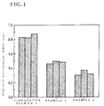
- FIG. 1 is a graph showing the surface roughness of different wafers polished according to Examples 1 and 2 and Comparative Example 1;
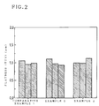
- FIG. 2 is a graph showing the flatness of the wafers polished according to Examples 1 and 2 and Comparative Example 1;
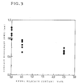
- FIG. 3 is a graph showing the relationship between the ethyl silicate content and the flatness of wafer surfaces determined by Examples 3 and 4 and Comparative Example 2; and
- FIG. 4 is an elevational view of an apparatus for polishing a wafer.
- The present invention will be described below in greater detail by way of the following examples which should be construed as illustrative rather than restrictive.
- FIG. 4 shows an
apparatus 1 for polishing a single crystal silicon wafer 70, to carry out polishing processes in Examples 1-4 and Comparative Exapmles 1-2. - In FIG. 4, the
apparatus 1 comprises arotary table assembly 2, a rotary wafer carrier 3, and a polishing agent supplying member 4. Therotary table assembly 2 comprises a rotary table 5 and apolishing pad 6 adhered on the upper surface of the rotary table 5. The rotary table 5 can rotate on ashaft 7 at a predetermined rotation speed by a driving device such as a motor. Thepolishing pad 6 comprises a polyurethane foam, a polyester, a nonwoven fabric or the like. The rotary wafer carrier 3 is for holding to carry the wafer 70 on thepolishing pad 6 of the rotary table asssembly 2 so that the surface of the wafer 70 faces to thepolishing pad 6. The wafer carrier 3 can rotate on a shaft 8 at a predetermined rotation speed and horizontally move on thepolishing pad 6 by an appropriate driving device such as a motor. During operation of theapparatus 1, the wafer 70 held by the wafer carrier 3 is in contact with thepolishing pad 6 and proper polishing loads are applied to the wafer 70 in a downward direction through the shaft 8 and the wafer carrier 3. The polishing agent supplying member 4 is for supplying a polishing agent 9 on thepolishing pad 6 to supply it betweeen the wafer 70 and thepolishing pad 6. The polishing agent 9 is a conventional colloidal silica agent or the present inventive agent. -
- · Sample wafers: Czochralski-grown p-type, 〈100〉-oriented, 150-mm-diameter, single crystal silicon wafer
- · Polishing pad: Nonwoven fabric (velour-type), hardness = 86 (Asker C-scale)
- · Polishing agent: 10.0 vol% of AJ-1325 (tradename for a stock solution of colloidal silica polishing agent manufactured by Nissan Chemical Industries, Ltd.), 2.5 vol% of Ethyl Silicate 28 (tradename for an ethyl silicate monomer manufactured by Colcoat, Inc.) and 87.5 vol% of pure water
- · Polishing load: 400 g/cm²
- · Polishing time: 10 min.
- Under the condition specified above, the sample wafers were polished. Then, surface roughness of the polished wafers was measured by means of an optical interference-type roughness tester (WYKOTOPO-3D, 250 µm□, manufactured by WYKO, Inc.). The results of this measurement (expressed in terms of root mean square) are shown in FIG. 1. Using a TTV (Total Thickness Variation) measuring device (ADE Microscan 8300 manufactured by ADE, Inc.), a measurement was made for flatness of the polished wafer surfaces with the results shown in FIG. 2. The TTV is difined as difference between the maximum and minimum values of thickness encountered in the polished wafer.
- Example 1 was repeated with the difference that the aforesaid polishing agent was formulated as containing 10.0 vol% of AJ-1325 specified above, 2.5 vol% of Ethyl Silicate 40 (tradename for an ethyl silicate polymer manufactured by Colcoat, Inc.), and 87.5 vol% of pure water. The results of the surface roughness measurement and the results of the flatness measurement are also shown in FIGs. 1 and 2, respectively.
- Example 1 was repeated by using a different polishing agent containing 10 vol% of AJ-1325 specified above, and 90 vol% of pure water. The results of the surface roughness measurement and the results of the flatness measurement are also shown in FIGs. 1 and 2, respectively.
- The results obtained from Examples 1 and 2 has proved that in terms of surface roughness and flatness (TTV), the wafer surfaces polished with the use of the polishing agents of this invention reached to the level of a surface obtained by final polishing.
- As is apparent from FIGs. 1 and 2, the polished wafer surfaces obtained by using the colloidal silica polishing agent of Comparative Example 1 are comparable to those of Examples 1 and 2 in respect of the flatness. But, regarding the surface roughness, the polished wafer surfaces of Comparative Example 1 are much poorer than those of Examples 1 and 2.
-
- · Sample wafers: Czochralski-grown p-type, 〈100〉-oriented, 150-mm-diameter, single crystal silicon wafer
- · Polishing pad: Nonwoven fabric (velour-type), hardness = 85 (Asker C-scale)
- · Polishing agent: AJ-1325 specified above (10 vol%) + Ethyl Silicate 28 specified above (selected vol% described below) + pure water (remainder)
- · Polishing load: 400 g/cm²
- · Polishing time: 10 min.
- To achieve Examples 3 and 4 and Comparative Example 2, the condition specified above was changed such that the amount of Ethyl Silicate 28 was selected as 0 vol% for Comparative Example 2, 0.5 vol% for Example 3, and 2.5 vol% for Example 4. In every Example, the pure water content was properly adjusted such that the total amount of the polishing agent was equal to 100 vol%. Under the condition selected for each Example, five sample wafers were polished and the polished sample wafers were measured for surface roughness in the same manner as Example 1. The results of the surface roughness measurement are shown in FIG. 3. As is apparent from FIG. 3, the surface roughness is greatly improved by Ethyl Silicate 28 contained, as an additive, in the polishing agent. This is true for both Examples 3 and 4 having different Ethyl Silicate 28 contents. The same effect has been confirmed by experiments even when n-type wafers have been used in place of the p-type wafers used in the examples described above.
- It is apparent from the foregoing description that a polishing agent of the present invention used in combination with a rigid polishing pad is able to provide, through a single-stage polishing process, a polished silicon wafer having an excellent flatness and whose surface has a roughness comparable to one obtained by the conventional final polishing process using a soft polishing pad. The present invention can obviate the use of the conventional final polishing process and hence is able to simplify the overall polishing process.
- Obviously, various minor changes and modifications of the present invention are possible in the light of the above teaching. It is therefore to be understood that within the scope of the appended claims the invention may be practiced otherwise than as specifically described.
Claims (4)
- A polishing agent for polishing a silicon wafer, characterized by a colloidal silica polishing agent containing an ethyl silicate monomer and/or an ethyl silicate polymer.
- A polishing agent according to claim 1, wherein the content of said ethyl silicate monomer and/or said ethyl silicate polymer is in the range of 0.1 to 10.0 percent by volume relative to the total amount of said colloidal silica polishing agent.
- A method of polishing a silicon wafer, characterized by using the polishing agent of claim 1 or 2 in combination with a rigid polishing pad.
- A method according to claim 3, wherein said polishing pad has a hardness in the range of 80 to 95 according to Ascar C-scale.
Applications Claiming Priority (2)
| Application Number | Priority Date | Filing Date | Title |
|---|---|---|---|
| JP12125094A JP2894208B2 (en) | 1994-06-02 | 1994-06-02 | Polishing agent for polishing silicon wafer and polishing method |
| JP121250/94 | 1994-06-02 |
Publications (2)
| Publication Number | Publication Date |
|---|---|
| EP0685877A2 true EP0685877A2 (en) | 1995-12-06 |
| EP0685877A3 EP0685877A3 (en) | 1997-01-08 |
Family
ID=14806619
Family Applications (1)
| Application Number | Title | Priority Date | Filing Date |
|---|---|---|---|
| EP95108481A Withdrawn EP0685877A3 (en) | 1994-06-02 | 1995-06-01 | Polishing agent used for polishing silicon wafers and polishing method using the same. |
Country Status (3)
| Country | Link |
|---|---|
| US (1) | US5667567A (en) |
| EP (1) | EP0685877A3 (en) |
| JP (1) | JP2894208B2 (en) |
Cited By (7)
| Publication number | Priority date | Publication date | Assignee | Title |
|---|---|---|---|---|
| EP0750335A2 (en) * | 1995-06-23 | 1996-12-27 | Shin-Etsu Handotai Co., Ltd | Polishing agent used for polishing semiconductor wafers and polishing method using the same |
| EP0779655A3 (en) * | 1995-12-14 | 1997-07-16 | International Business Machines Corporation | A method of chemically-mechanically polishing an electronic component |
| WO1997026114A1 (en) * | 1996-01-22 | 1997-07-24 | Micron Technology, Inc. | A polishing pad and a method for making a polishing pad with covalently bonded particles |
| EP0782179A3 (en) * | 1995-12-27 | 1997-07-30 | Shin-Etsu Handotai Co., Ltd | Method of manufacturing semiconductor mirror wafers |
| US5938801A (en) * | 1997-02-12 | 1999-08-17 | Micron Technology, Inc. | Polishing pad and a method for making a polishing pad with covalently bonded particles |
| CN102382576A (en) * | 2011-11-10 | 2012-03-21 | 江南大学 | Ultrasonic atomization alkaline polishing solution |
| CN105462504A (en) * | 2015-12-11 | 2016-04-06 | 蓝思科技(长沙)有限公司 | C-direction sapphire polishing solution and preparation method thereof |
Families Citing this family (3)
| Publication number | Priority date | Publication date | Assignee | Title |
|---|---|---|---|---|
| GB2316414B (en) * | 1996-07-31 | 2000-10-11 | Tosoh Corp | Abrasive shaped article, abrasive disc and polishing method |
| KR100615691B1 (en) | 1998-12-18 | 2006-08-25 | 도소 가부시키가이샤 | A member for polishing, surface plate for polishing and polishing method using the same |
| KR100637887B1 (en) | 1998-12-28 | 2006-10-23 | 도소 가부시키가이샤 | Molded body for polishing, surface plate for polishing and polishing method using the same |
Family Cites Families (13)
| Publication number | Priority date | Publication date | Assignee | Title |
|---|---|---|---|---|
| JPS598776A (en) * | 1982-07-08 | 1984-01-18 | Toshiba Silicone Co Ltd | Lustering agent composition |
| SU1189668A1 (en) * | 1983-10-05 | 1985-11-07 | Предприятие П/Я В-2998 | Compound for manufacturing abrasive tool and method of manufacturing same |
| US4579564A (en) * | 1985-01-18 | 1986-04-01 | Smith Robert S | Polishing pad for a fine finish |
| SU1373551A1 (en) * | 1986-07-01 | 1988-02-15 | Уральский филиал Всесоюзного научно-исследовательского института абразивов и шлифования | Method of producing abrasive tools |
| SU1371891A1 (en) * | 1986-08-25 | 1988-02-07 | Харьковский политехнический институт им.В.И.Ленина | Ceramic binder for manufacturing abrasive tools |
| JPS6374911A (en) * | 1986-09-19 | 1988-04-05 | Shin Etsu Chem Co Ltd | Production of fine spherical silica |
| US5226930A (en) * | 1988-06-03 | 1993-07-13 | Monsanto Japan, Ltd. | Method for preventing agglomeration of colloidal silica and silicon wafer polishing composition using the same |
| JPH029571A (en) * | 1988-06-28 | 1990-01-12 | Fujitsu Ltd | Two-side polishing method |
| US5352277A (en) * | 1988-12-12 | 1994-10-04 | E. I. Du Pont De Nemours & Company | Final polishing composition |
| JP2714411B2 (en) * | 1988-12-12 | 1998-02-16 | イー・アイ・デュポン・ドゥ・ヌムール・アンド・カンパニー | Composition for fine polishing of wafers |
| JPH03108650A (en) * | 1989-09-22 | 1991-05-08 | Seiko Epson Corp | Manufacture of humidity sensor element |
| JP3290189B2 (en) * | 1991-04-11 | 2002-06-10 | 旭電化工業株式会社 | Polishing method of silicon wafer |
| EP0520109B1 (en) * | 1991-05-28 | 1995-03-29 | Rodel, Inc. | Low sodium, low metals silica polishing slurries |
-
1994
- 1994-06-02 JP JP12125094A patent/JP2894208B2/en not_active Expired - Fee Related
-
1995
- 1995-06-01 EP EP95108481A patent/EP0685877A3/en not_active Withdrawn
-
1996
- 1996-12-16 US US08/755,802 patent/US5667567A/en not_active Expired - Fee Related
Non-Patent Citations (1)
| Title |
|---|
| None |
Cited By (12)
| Publication number | Priority date | Publication date | Assignee | Title |
|---|---|---|---|---|
| EP0750335A2 (en) * | 1995-06-23 | 1996-12-27 | Shin-Etsu Handotai Co., Ltd | Polishing agent used for polishing semiconductor wafers and polishing method using the same |
| EP0750335A3 (en) * | 1995-06-23 | 1998-09-23 | Shin-Etsu Handotai Co., Ltd | Polishing agent used for polishing semiconductor wafers and polishing method using the same |
| US5866226A (en) * | 1995-06-23 | 1999-02-02 | Shin-Etsu Handotai Co., Ltd. | Polishing agent used for polishing semiconductor wafers and polishing method using the same |
| EP0779655A3 (en) * | 1995-12-14 | 1997-07-16 | International Business Machines Corporation | A method of chemically-mechanically polishing an electronic component |
| EP0782179A3 (en) * | 1995-12-27 | 1997-07-30 | Shin-Etsu Handotai Co., Ltd | Method of manufacturing semiconductor mirror wafers |
| US5821167A (en) * | 1995-12-27 | 1998-10-13 | Shin-Etsu Handotai Co., Ltd. | Method of manufacturing semiconductor mirror wafers |
| WO1997026114A1 (en) * | 1996-01-22 | 1997-07-24 | Micron Technology, Inc. | A polishing pad and a method for making a polishing pad with covalently bonded particles |
| US5823855A (en) * | 1996-01-22 | 1998-10-20 | Micron Technology, Inc. | Polishing pad and a method for making a polishing pad with covalently bonded particles |
| US5879222A (en) * | 1996-01-22 | 1999-03-09 | Micron Technology, Inc. | Abrasive polishing pad with covalently bonded abrasive particles |
| US5938801A (en) * | 1997-02-12 | 1999-08-17 | Micron Technology, Inc. | Polishing pad and a method for making a polishing pad with covalently bonded particles |
| CN102382576A (en) * | 2011-11-10 | 2012-03-21 | 江南大学 | Ultrasonic atomization alkaline polishing solution |
| CN105462504A (en) * | 2015-12-11 | 2016-04-06 | 蓝思科技(长沙)有限公司 | C-direction sapphire polishing solution and preparation method thereof |
Also Published As
| Publication number | Publication date |
|---|---|
| JPH07326597A (en) | 1995-12-12 |
| EP0685877A3 (en) | 1997-01-08 |
| US5667567A (en) | 1997-09-16 |
| JP2894208B2 (en) | 1999-05-24 |
Similar Documents
| Publication | Publication Date | Title |
|---|---|---|
| US6352927B2 (en) | Semiconductor wafer and method for fabrication thereof | |
| EP0690772B1 (en) | Compositions and methods for polishing and planarizing surfaces | |
| JP3317330B2 (en) | Manufacturing method of semiconductor mirror surface wafer | |
| JP5557506B2 (en) | Polishing both sides of a semiconductor wafer | |
| JP2004507085A (en) | Method and apparatus for processing a semiconductor wafer using a novel final polishing method | |
| EP0685877A2 (en) | Polishing agent used for polishing silicon wafers and polishing method using the same | |
| US20110223840A1 (en) | Polishing Composition and Polishing Method Using The Same | |
| MY133700A (en) | Polishing fluid composition and polishing method | |
| US5827395A (en) | Polishing pad used for polishing silicon wafers and polishing method using the same | |
| EP0373501A3 (en) | Fine polishing composition for wafers | |
| EP1566421A3 (en) | CMP abrasive, liquid additive for CMP abrasive and method for polishing substrate. | |
| EP0850724B1 (en) | Surface grinding device and method of surface-grinding a thin-plate workpiece | |
| JP2012060149A (en) | Method for polishing substrate composed of semiconductor material | |
| JP2011103460A (en) | Method for polishing semiconductor wafer | |
| KR930004114B1 (en) | Polishing method and abrasive for semiconductor device treatment | |
| JPWO2003070853A1 (en) | Polishing slurry | |
| US5891353A (en) | Polishing agent used for polishing semiconductor wafers and polishing method using the same | |
| US20050095865A1 (en) | Selective chemical-mechanical polishing properties of a cross-linked polymer and specific applications therefor | |
| KR100792066B1 (en) | Removal method for planarizing the semiconductor wafer | |
| JP2001156030A (en) | Grinding roller for semiconductor wafer and method for grinding semiconductor wafer using the same | |
| WO2017141704A1 (en) | Double-side polishing method and double-side polishing device | |
| EP1316991A1 (en) | Method of polishing semiconductor wafer | |
| JP3601937B2 (en) | Surface flattening method and surface flattening device | |
| JPH0319336A (en) | Polishing of semiconductor wafer | |
| JP2019150916A (en) | Polishing pad |
Legal Events
| Date | Code | Title | Description |
|---|---|---|---|
| PUAI | Public reference made under article 153(3) epc to a published international application that has entered the european phase |
Free format text: ORIGINAL CODE: 0009012 |
|
| AK | Designated contracting states |
Kind code of ref document: A2 Designated state(s): DE FR GB |
|
| PUAL | Search report despatched |
Free format text: ORIGINAL CODE: 0009013 |
|
| AK | Designated contracting states |
Kind code of ref document: A3 Designated state(s): DE FR GB |
|
| 17P | Request for examination filed |
Effective date: 19970218 |
|
| STAA | Information on the status of an ep patent application or granted ep patent |
Free format text: STATUS: THE APPLICATION HAS BEEN WITHDRAWN |
|
| 18W | Application withdrawn |
Withdrawal date: 20020422 |