EP0691643A1 - Electrical control device with crosstalk cancelling and its application with magnetic recording/reproducing heads - Google Patents
Electrical control device with crosstalk cancelling and its application with magnetic recording/reproducing heads Download PDFInfo
- Publication number
- EP0691643A1 EP0691643A1 EP95401526A EP95401526A EP0691643A1 EP 0691643 A1 EP0691643 A1 EP 0691643A1 EP 95401526 A EP95401526 A EP 95401526A EP 95401526 A EP95401526 A EP 95401526A EP 0691643 A1 EP0691643 A1 EP 0691643A1
- Authority
- EP
- European Patent Office
- Prior art keywords
- resistive
- elements
- resistive element
- layer
- limiting
- Prior art date
- Legal status (The legal status is an assumption and is not a legal conclusion. Google has not performed a legal analysis and makes no representation as to the accuracy of the status listed.)
- Granted
Links
- 230000008878 coupling Effects 0.000 claims abstract description 26
- 238000010168 coupling process Methods 0.000 claims abstract description 26
- 238000005859 coupling reaction Methods 0.000 claims abstract description 26
- 239000000758 substrate Substances 0.000 claims abstract description 10
- 239000003990 capacitor Substances 0.000 claims description 11
- 239000011159 matrix material Substances 0.000 claims description 10
- 239000003989 dielectric material Substances 0.000 claims description 6
- 239000004020 conductor Substances 0.000 claims 8
- 238000013500 data storage Methods 0.000 abstract 1
- 238000004804 winding Methods 0.000 description 18
- 238000001465 metallisation Methods 0.000 description 10
- 230000000875 corresponding effect Effects 0.000 description 2
- 230000001627 detrimental effect Effects 0.000 description 2
- 235000021183 entrée Nutrition 0.000 description 2
- 238000000034 method Methods 0.000 description 2
- 230000003071 parasitic effect Effects 0.000 description 2
- 238000002679 ablation Methods 0.000 description 1
- 230000000996 additive effect Effects 0.000 description 1
- 238000010276 construction Methods 0.000 description 1
- 230000002596 correlated effect Effects 0.000 description 1
- 238000010586 diagram Methods 0.000 description 1
- 230000001939 inductive effect Effects 0.000 description 1
- 230000010354 integration Effects 0.000 description 1
- 238000004519 manufacturing process Methods 0.000 description 1
- 230000003287 optical effect Effects 0.000 description 1
Images


Classifications
-
- G—PHYSICS
- G11—INFORMATION STORAGE
- G11B—INFORMATION STORAGE BASED ON RELATIVE MOVEMENT BETWEEN RECORD CARRIER AND TRANSDUCER
- G11B5/00—Recording by magnetisation or demagnetisation of a record carrier; Reproducing by magnetic means; Record carriers therefor
- G11B5/127—Structure or manufacture of heads, e.g. inductive
- G11B5/29—Structure or manufacture of unitary devices formed of plural heads for more than one track
-
- G—PHYSICS
- G11—INFORMATION STORAGE
- G11B—INFORMATION STORAGE BASED ON RELATIVE MOVEMENT BETWEEN RECORD CARRIER AND TRANSDUCER
- G11B20/00—Signal processing not specific to the method of recording or reproducing; Circuits therefor
- G11B20/10—Digital recording or reproducing
- G11B20/18—Error detection or correction; Testing, e.g. of drop-outs
-
- G—PHYSICS
- G11—INFORMATION STORAGE
- G11B—INFORMATION STORAGE BASED ON RELATIVE MOVEMENT BETWEEN RECORD CARRIER AND TRANSDUCER
- G11B23/00—Record carriers not specific to the method of recording or reproducing; Accessories, e.g. containers, specially adapted for co-operation with the recording or reproducing apparatus ; Intermediate mediums; Apparatus or processes specially adapted for their manufacture
- G11B23/0007—Circuits or methods for reducing noise, for correction of distortion, or for changing density of recorded information
-
- G—PHYSICS
- G11—INFORMATION STORAGE
- G11B—INFORMATION STORAGE BASED ON RELATIVE MOVEMENT BETWEEN RECORD CARRIER AND TRANSDUCER
- G11B5/00—Recording by magnetisation or demagnetisation of a record carrier; Reproducing by magnetic means; Record carriers therefor
- G11B5/48—Disposition or mounting of heads or head supports relative to record carriers ; arrangements of heads, e.g. for scanning the record carrier to increase the relative speed
- G11B5/4806—Disposition or mounting of heads or head supports relative to record carriers ; arrangements of heads, e.g. for scanning the record carrier to increase the relative speed specially adapted for disk drive assemblies, e.g. assembly prior to operation, hard or flexible disk drives
- G11B5/484—Integrated arm assemblies, e.g. formed by material deposition or by etching from single piece of metal or by lamination of materials forming a single arm/suspension/head unit
-
- G—PHYSICS
- G11—INFORMATION STORAGE
- G11B—INFORMATION STORAGE BASED ON RELATIVE MOVEMENT BETWEEN RECORD CARRIER AND TRANSDUCER
- G11B5/00—Recording by magnetisation or demagnetisation of a record carrier; Reproducing by magnetic means; Record carriers therefor
- G11B5/48—Disposition or mounting of heads or head supports relative to record carriers ; arrangements of heads, e.g. for scanning the record carrier to increase the relative speed
- G11B5/49—Fixed mounting or arrangements, e.g. one head per track
- G11B5/4969—Details for track selection or addressing
Definitions
- the invention relates to an electrical control device with crosstalk correction and its application to magnetic recording / reading heads.
- a source or a matrix of electrically controllable devices such as electromagnetic devices (magnetic heads for example) or optical devices to compensate for crosstalk that may exist between neighboring devices.
- the invention consists of a physical and passive device associated with an arrangement of elements making it possible to compensate electrically for the magnetic crosstalk which exists in the multi-track writing component on magnetic media. .
- This device replaces a set of passive components - resistors and capacitors associated with their connection - placed between the electronics for writing write currents and the coils of the writing component.
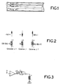
- the invention applies in the context of a system for recording and reading data on magnetic media, where the physical format for writing data on tape is of the multi-track type in parallel, as shown in FIG. 1 .
- Magnetic crosstalk in writing is manifested by a partial writing of the data normally intended for a track J on the neighboring tracks J-1 and J + 1.
- a multi-track magnetic recorder has a large number of magnetic heads (1024 for example) used to write 1024 tracks on a tape 12.54 mm high.
- Such a device has a matrix structure; the 1024 magnetic air gaps are distributed over a parallelogram 16 columns long and 64 lines high.
- this parallelogram - essentially the angle - is judiciously chosen to carry out the writing of the 1024 tracks on the magnetic tape in an adjacent manner and without overlap between tracks.
- Each column and each line has an electrically addressed coil.
- the currents flowing through the columns and the rows do not generate a sufficient field for writing on tape at the location of the corresponding air gaps.
- the additive action of the currents makes it possible to generate in the corresponding air gap a sufficient field for writing data on tape.
- Bd kd x B, where kd represents the cross-talk coefficient between columns of the writing head.
- Crosstalk in writing is very detrimental to the quality of the channel, because the data on replay is tainted by noise correlated to neighboring tracks which strongly degrades the signal to noise ratio.
- FIG. 3 illustrates the electrical assembly used.
- Capacitor C of low value, is intended to increase the rise time of the current in the windings.
- the common point of the windings fixed at + V2 makes it possible to create currents + I and -I from a single voltage.
- French Patent Application No. 92 15472 describes a device providing coupling resistors to compensate for crosstalk.
- the crosstalk created by the coil J is corrected by injecting into J-1 and J + 1 the current which gives rise to a field opposite to the crosstalk field in J-1 and J + 1: the magnetic polarity inversion from one winding to the other determines a correction current in J-1 and J + 1 with the same sign as that in J, since the phase opposition is carried out by wiring.
- the component crosstalk correction can then be carried out only with passive components, as shown in FIG. 5.
- the crosstalk correction resistors, Rd derive a part kd of the current from J to J-1 and J + 1, and give rise to the magnetic field which cancels the parasitic field.
- the write component requires a network of 288 resistors to function properly.
- the object of the invention is to simplify the design and construction of the crosstalk correction circuits and even to reduce the number of resistors required.
- the invention therefore relates to an electrical control device with crosstalk correction comprising several devices electrically controllable each by a limiting resistor, characterized in that the current limiting resistors are resistive elements for limiting in flat layers arranged on a first face. substrate and in that it also comprises at least one resistive coupling element disposed transversely to each resistive element and interconnecting these resistive elements.
- the invention is applicable to the control of a matrix recording / reading head.
- the device proposed to replace all of the current limiting and crosstalk resistors is a resistive surface having an anisotropy of resistivity along its X and Y axes. This anisotropy is obtained either by a form factor of the device, or by a choice of resistive patterns that intersect at 90 degrees.
- the simplest structure fulfilling the function is a rectangular surface with a certain ohmic resistance per "square".
- FIG. 7 shows the structure in the so-called bridge configuration.
- the electromagnetic devices to be controlled are represented by the windings B1 to B5. As can be seen by the signs "+" and "-" associated with their accesses, these windings have alternating winding directions as has been explained in relation to FIGS. 5 and 6.
- Control circuits send at low impedance the voltages + V and 0 on each of the network inputs: the length "a" sizes the resistance ⁇ 2 which will carry out the current limitation i1 in each winding, of very low impedance Z, while the distance between pads "b” determines the proportion id of the main current which is derived towards the neighboring windings.
- This structure performs analog mixing of current, inter-windings.
- the 288 resistors are replaced by 3 "resistive mixers"; 1 for all 64 rows, and 2 for the 16 columns which are addressed in a bridge.
- the ratio of dimensions (a: b) which determines the kd of the device can lead to a dimensioning of the assembly incompatible with the environment of the component.
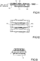
- a structure is made up of two resistive layers in crossed contact, each made up of parallel strips of different resistances, as shown in FIG. 8.
- the geometric dimensioning of the device is then independent of its electrical characteristics.
- Elements such as ⁇ 1 represent resistive current limiting elements connecting each electromagnetic device B1 to Bn to be controlled by the control circuits.
- the element such as ⁇ 2 represented perpendicularly to ⁇ 1 is a resistive coupling element in electrical contact with each resistive current limiting element ⁇ 1.
- the resistive elements ⁇ 1 are produced in a thin or thick layer on a substrate plate.
- the ⁇ 2 elements are also produced in a thin or thick layer on the ⁇ 1 elements and on the substrate plate.
- the calibration of the dimensions in thickness and in particular in width makes it possible to adjust the values of the resistances.
- the number of elements ⁇ 2 makes it possible to adjust the coupling.
- the resistive coupling element can be pre-formed, as shown in FIG. 9 to take into account a characteristic constant of the component to be corrected.
- the element ⁇ 2 has a shape adapted to the couplings to be produced.
- slots are provided in the element ⁇ 2 to adjust the resistive couplings between elements ⁇ 1 as desired.
- the device can be adjusted by laser, and this at the level of each winding, by partial ablation of the resistive layers for adjustment of the main current and of the crosstalk correction currents.
- FIGS. 10a and 10b represent an alternative embodiment of the invention in which resistive elements such as ⁇ 2 and ⁇ '2 are provided connecting the access of each resistive element ⁇ 1 on the control circuit side to the access on the winding side of the elements immediately adjacent resistives. A resistive coupling between input and output is thus obtained as shown in FIGS. 5 and 6.
- FIG. 10b represents a sectional view which shows that the resistive elements ⁇ 2 and ⁇ '2 are isolated from each other by an insulating layer 11.
- the section in FIG. 11 shows a type of embodiment allowing this component to be integrated into the device.
- the capacitive coupling is carried out by two facing metallization layers. This device is reproduced for each winding command.
- FIG. 11 is a simplified representation of such an embodiment. It is applied to the device of FIG. 8 comprising several resistive coupling elements ⁇ 2.
- This device comprises on the back of the ⁇ 1 element, a first metallization M1 connected to one end of the ⁇ 1 element and a second metallization M2 connected to the other end of the ⁇ 1 element. Between the two metallizations is provided a dielectric material C1.
- the resistive elements ⁇ 1 and ⁇ 2 can be produced on one face of a substrate and the capacitors constituted by the metallizations M1, M2 and the dielectric C1 can be produced on the opposite face of the substrate.
- FIG. 12 shows a device according to the invention in which coupling capacitors are provided between the inputs of the resistive elements ⁇ 1 and the outputs of the neighboring resistive elements.
- the resistive coupling elements ⁇ 2 have not been shown.
- Each metallization M1 associated with a resistive element ⁇ 1 has a conductive tab L1, L'1 on each side of the metallization which extends towards the metallization M1 of the neighboring resistive element.
- each metallization M2 which has tabs N1 and N'1.
- Each tab L1, L'1 of a resistive element is located above a tab N1 or N'1 of a neighboring resistive element and the two tabs are separated by a dielectric material so as to form a capacitor. Capacitors are thus produced in parallel with the resistive coupling elements ⁇ 2 whose value depends on the facing surface.
- FIG. 13 shows an example of integration of the control device described above with a matrix magnetic head produced in the form of a plate P.
- One face of the plate P1 has the poles of the magnetic heads and the air gaps. This face therefore serves as an active face.
- the previously described control device produced in the form of a plate P2 is attached to the main face of the plate P1 opposite the active face.
- a matrix magnetic head can be produced as described in French Patent Application No. 2,648,940 and a P2 plate is attached thereto then provision is made for connecting the coils to the circuits of the P2 plate.
Abstract
Description
L'invention concerne un dispositif de commande électrique à correction de diaphonie et son application à des têtes magnétiques d'enregistrement/lecture.The invention relates to an electrical control device with crosstalk correction and its application to magnetic recording / reading heads.
Elle est applicable à une source ou une matrice de dispositifs commandables électriquement tels que des dispositifs électromagnétiques (têtes magnétiques par exemple) ou des dispositifs optiques pour compenser la diaphonie pouvant exister entre dispositifs voisins.It is applicable to a source or a matrix of electrically controllable devices such as electromagnetic devices (magnetic heads for example) or optical devices to compensate for crosstalk that may exist between neighboring devices.
Dans le cas de têtes magnétiques d'enregistrement/lecture, l'invention consiste en un dispositif physique et passif associé à une disposition d'éléments permettant de compenser électriquement la diaphonie magnétique qui existe dans le composant d'écriture multi-piste sur média magnétique.In the case of magnetic recording / reading heads, the invention consists of a physical and passive device associated with an arrangement of elements making it possible to compensate electrically for the magnetic crosstalk which exists in the multi-track writing component on magnetic media. .
Ce dispositif remplace un ensemble de composants passifs - résistances et capacités associées à leur connectique- disposés entre l'électronique de génération des courants d'écriture et les bobinages du composant d'écriture.This device replaces a set of passive components - resistors and capacitors associated with their connection - placed between the electronics for writing write currents and the coils of the writing component.
L'invention s'applique dans le cadre d'un système d'enregistrement et lecture de données sur média magnétique, où le format physique d'écriture des données sur bande est du type multi-pistes en parallèle, comme représenté sur la figure 1.The invention applies in the context of a system for recording and reading data on magnetic media, where the physical format for writing data on tape is of the multi-track type in parallel, as shown in FIG. 1 .
Lorsque ces pistes sont très rapprochées, le composant qui permet d'écrire selon ce format a une diaphonie à l'écriture qui devient préjudiciable à la qualité des données écrites.When these tracks are very close together, the component which makes it possible to write in this format has a crosstalk in the writing which becomes detrimental to the quality of the written data.
La diaphonie magnétique à l'écriture se manifeste par une écriture partielle des données normalement destinée à une piste J sur les pistes voisines J-1 et J+1.Magnetic crosstalk in writing is manifested by a partial writing of the data normally intended for a track J on the neighboring tracks J-1 and J + 1.
Par exemple un enregistreur magnétique multi-piste comporte un grand nombre de têtes magnétiques (1024 par exemple) permet d'écrire 1024 pistes sur une bande de 12,54 mm de hauteur. Un tel dispositif possède une structure matricielle ; les 1024 entrefers magnétiques sont répartis sur un parallélogramme de 16 colonnes de long et de 64 lignes de haut.For example, a multi-track magnetic recorder has a large number of magnetic heads (1024 for example) used to write 1024 tracks on a tape 12.54 mm high. Such a device has a matrix structure; the 1024 magnetic air gaps are distributed over a parallelogram 16 columns long and 64 lines high.
La forme géométrique de ce parallélogramme -essentiellement l'angle- est judicieusement choisi pour réaliser l'écriture des 1024 pistes sur la bande magnétique de façon adjacente et sans recouvrement entre pistes.The geometric shape of this parallelogram - essentially the angle - is judiciously chosen to carry out the writing of the 1024 tracks on the magnetic tape in an adjacent manner and without overlap between tracks.
Chaque colonne et chaque ligne possède un bobinage adressé électriquement. En fonctionnement nominal, les courants parcourant les colonnes et les lignes ne génèrent pas un champ suffisant pour l'écriture sur bande à l'endroit des entrefers leur correspondant. En revanche, au croisement d'une colonne et d'une ligne, l'action additive des courants permet de générer dans l'entrefer correspondant un champ suffisant pour l'écriture d'une donnée sur bande.Each column and each line has an electrically addressed coil. In nominal operation, the currents flowing through the columns and the rows do not generate a sufficient field for writing on tape at the location of the corresponding air gaps. On the other hand, at the intersection of a column and a row, the additive action of the currents makes it possible to generate in the corresponding air gap a sufficient field for writing data on tape.
Dans la réalité, lorsqu'une colonne (ou ligne) J est adressée électriquement par un courant +I, apparaît dans tous les entrefers de la colonne (ou de la ligne) excitée un champ magnétique B proportionnel à ce courant :
B = k x I, où k représente l'efficacité de la tête d'écriture.In reality, when a column (or line) J is electrically addressed by a current + I, appears in all the air gaps of the excited column (or line) a magnetic field B proportional to this current:
B = kx I, where k represents the efficiency of the writing head.
Dû aux fuites des circuits magnétiques du composant, apparaît également sur les entrefers situés sur les colonnes voisines, un champ parasite de diaphonie Bd qui est une proportion positive de B.Due to the leakage of the magnetic circuits of the component, also appears on the air gaps located on the neighboring columns, a parasitic field of crosstalk Bd which is a positive proportion of B.
Bd = kd x B, où kd représente le coefficient de diaphonie entre colonnes de la tête d'écriture.Bd = kd x B, where kd represents the cross-talk coefficient between columns of the writing head.
Lorsque en fonctionnement nominal, ces champs de diaphonie qui existent pour toutes les colonnes et lignes de la tête se superposent à ceux créés par les courants, toute piste J se voit partiellement écrite avec les signaux des pistes physiquement voisines.When in nominal operation, these crosstalk fields which exist for all the columns and rows of the head are superimposed on those created by the currents, any track J is partially written with the signals of the physically neighboring tracks.
La diaphonie à l'écriture est très néfaste à la qualité du canal, car les données à la relecture sont entachées d'un bruit corrélé aux pistes voisines qui dégrade fortement le rapport signal à bruit.Crosstalk in writing is very detrimental to the quality of the channel, because the data on replay is tainted by noise correlated to neighboring tracks which strongly degrades the signal to noise ratio.
Le processus qui donne naissance à la diaphonie dans le composant étant linéaire et réciproque (Bd = kd x k x I), on peut annuler le champ Bd sur les colonnes J-1 et J+1 par l'envoi d'un courant -kd x I de polarité inverse, dans ces colonnes lors de l'adressage de la colonne J par le courant I (voir figure 2).The process which gives rise to crosstalk in the component being linear and reciprocal (Bd = kd xkx I), we can cancel the field Bd on columns J-1 and J + 1 by sending a current -kd x I of reverse polarity, in these columns during the addressing of column J by the current I (see FIG. 2).
D'un point de vue électrique, cette solution est compliquée car il faut de façon synchrone générer des courants de polarités opposées, donc des circuits de commande symétriques et linéaires puisque le courant est proportionnel à kd.From an electrical point of view, this solution is complicated because it is necessary to synchronously generate currents of opposite polarities, therefore symmetrical and linear control circuits since the current is proportional to kd.
Cette solution n'est pas envisageable pour des raisons de dissipation de puissance car le nombre de circuits de commande nécessaires est élevé (I lignes + J colonnes) ; ce sont donc des circuits de commande simplifiés à deux états 0 volt --> + V volts qui alimentent le bobinage à travers une résistance.This solution cannot be envisaged for reasons of power dissipation because the number of control circuits required is high (I rows + J columns); these are therefore simplified control circuits with two
La figure 3 illustre le montage électrique utilisé. La capacité C, de faible valeur, est destinée à augmenter le temps de montée du courant dans les bobinages. Le point commun des bobinages fixé à + V2 permet de créer des courants +I et -I à partir d'une seule tension.Figure 3 illustrates the electrical assembly used. Capacitor C, of low value, is intended to increase the rise time of the current in the windings. The common point of the windings fixed at + V2 makes it possible to create currents + I and -I from a single voltage.
La contrainte sur la nature des circuits de commande impose donc une autre solution qui permet la correction de diaphonie magnétique avec le respect de polarité.The constraint on the nature of the control circuits therefore imposes another solution which allows the correction of crosstalk with respect for polarity.
La Demande de Brevet français n° 92 15472 décrit un dispositif prévoyant des résistances de couplage pour compenser la diaphonie.French Patent Application No. 92 15472 describes a device providing coupling resistors to compensate for crosstalk.
Dans la configuration de base, tous les bobinages du composant présentent une phase magnétique identique, c'est-à-dire qu'un courant +I ferait naître dans tous les entrefers un champ +B = +k x I : dans ces conditions le courant de correction reste Id = -kd x I de signe opposé.In the basic configuration, all of the component's windings have an identical magnetic phase, that is to say that a current + I would give rise in all the air gaps to a field + B = + kx I: under these conditions the current of correction remains Id = -kd x I of opposite sign.
En alternant la phase magnétique d'un bobinage sur deux sur tout le composant, donc avec un bobinage bobiné dans un sens, puis le suivant en sens inverse, il faut également alterner le signe du courant pour générer un champ magnétique de même signe sur tous les entrefers.By alternating the magnetic phase of a winding on two on all the component, therefore with a winding wound in one direction, then the next in opposite direction, it is also necessary to alternate the sign of the current to generate a magnetic field of the same sign on all the air gaps.
Ce principe est appliqué sur l'ensemble des lignes et colonnes du composant. On remarque sur les figures 4a à 4d qu'une information électrique +1 donne bien un champ magnétique +B dans l'entrefer.This principle is applied to all the rows and columns of the component. Note in FIGS. 4a to 4d that electrical information +1 gives a magnetic field + B in the air gap.
Dans cette configuration, on corrige la diaphonie créée par la bobine J en injectant dans J-1 et J+1 le courant qui fait naître un champ inverse au champ de diaphonie en J-1 et J+1 : l'inversion de polarité magnétique d'un bobinage à l'autre détermine un courant de correction en J-1 et J+1 de même signe que celui en J, puisque l'opposition de phase est réalisée par câblage.In this configuration, the crosstalk created by the coil J is corrected by injecting into J-1 and J + 1 the current which gives rise to a field opposite to the crosstalk field in J-1 and J + 1: the magnetic polarity inversion from one winding to the other determines a correction current in J-1 and J + 1 with the same sign as that in J, since the phase opposition is carried out by wiring.
La correction de diaphonie du composant est alors réalisable uniquement avec des composants passifs, comme représenté sur la figure 5. Les résistances de correction de diaphonie, Rd dérivent une partie kd du courant de J vers J-1 et J+1, et font naître le champ magnétique qui annule le champ parasite.The component crosstalk correction can then be carried out only with passive components, as shown in FIG. 5. The crosstalk correction resistors, Rd derive a part kd of the current from J to J-1 and J + 1, and give rise to the magnetic field which cancels the parasitic field.
Dans le cas où on réalise un circuit de commande symétrique pour des raisons de temps de montée du courant dans une impédance selfique, le nombre de composants est doublé, et le schéma d'un tel circuit est alors représenté en figure 6.In the case where a symmetrical control circuit is produced for reasons of time for the current to rise in an inductive impedance, the number of components is doubled, and the diagram of such a circuit is then represented in FIG. 6.
Dans le cas d'une tête magnétique matricielle comportant 1024 entrefers d'écriture répartis en 16 colonnes et 64 lignes, le montage électrique emploie 64 circuits de commande simples pour les lignes et 16 circuits de commande en pont pour les colonnes : cette configuration demande :
- 64 + 2x16 = 96 circuits de commande
- 64 = 2x16 = 96 résistances de contrôle du courant des bobinages
- 2x64 + 4x16 = 192 résistances de correction de diaphonie.
- 64 + 2x16 = 96 control circuits
- 64 = 2x16 = 96 winding current control resistors
- 2x64 + 4x16 = 192 crosstalk correction resistors.
Le composant d'écriture nécessite un réseau de 288 résistances pour fonctionner correctement.The write component requires a network of 288 resistors to function properly.
L'invention a pour objet de simplifier la conception et la réalisation des circuits de correction de diaphonie et même de réduire le nombre de résistances nécessaires.The object of the invention is to simplify the design and construction of the crosstalk correction circuits and even to reduce the number of resistors required.
L'invention concerne donc un dispositif de commande électrique à correction de diaphonie comprenant plusieurs dispositifs commandables électriquement chacun par une résistance de limitation, caractérisé en ce que les résistances de limitation de courant sont des éléments résistifs de limitation en couches planes disposés sur une première face de substrat et en ce qu'il comporte également au moins un élément résistif de couplage disposé transversalement à chaque élément résistif et interconnectant ces éléments résistifs.The invention therefore relates to an electrical control device with crosstalk correction comprising several devices electrically controllable each by a limiting resistor, characterized in that the current limiting resistors are resistive elements for limiting in flat layers arranged on a first face. substrate and in that it also comprises at least one resistive coupling element disposed transversely to each resistive element and interconnecting these resistive elements.
L'invention concerne également un dispositif caractérisé en ce qu'il comporte :
- un premier ensemble d'éléments résistifs de couplage connectant chacune une entrée d'un élément résistif de limitation rang pair à une sortie d'un élément résistif de limitation voisin de rang impair ;
- un deuxième ensemble d'éléments résistifs isolés des premiers connectant chacun une sortie d'un élément résistif de limitation de rang pair à une entrée d'un élément résistif de limitation de rang impair.
- a first set of resistive coupling elements each connecting an input of a resistive element of limiting rank even with an output of a resistive limiting element neighboring of odd rank;
- a second set of resistive elements isolated from the first, each connecting an output of a resistive element of rank limitation even with an input of a resistive element of limitation of odd rank.
L'invention est applicable à la commande d'une tête matricielle d'enregistrement/lecture.The invention is applicable to the control of a matrix recording / reading head.
Les différents objets et caractéristiques de l'invention apparaîtront plus clairement dans la description qui va suivre et dans les figures annexées qui représentent :
- les figures 1 à 6, des dispositifs de commande électromagnétiques connus dans la technique ;
- la figure 7, un exemple général du dispositif de commande à correction de diaphonie selon l'invention ;
- la figure 8, un autre mode de réalisation du dispositif de commande selon l'invention ;
- la figure 9, une variante de réalisation du dispositif de la figure 8 ;
- les figures 10a et 10b, un mode de réalisation plus complexe du dispositif de commande selon l'invention ;
- la figure 11, un dispositif de commande comportant un condensateur en parallèle avec chaque élément résistif de limitation de courant ;
- la figure 12, un dispositif de commande comportant des condensateurs en parallèle avec les éléments résistifs de couplage ;
- la figure 13, un exemple d'application à une tête matricielle.
- Figures 1 to 6, electromagnetic control devices known in the art;
- FIG. 7, a general example of the crosstalk correction control device according to the invention;
- Figure 8, another embodiment of the control device according to the invention;
- Figure 9, an alternative embodiment of the device of Figure 8;
- Figures 10a and 10b, a more complex embodiment of the control device according to the invention;
- FIG. 11, a control device comprising a capacitor in parallel with each resistive current limiting element;
- FIG. 12, a control device comprising capacitors in parallel with the resistive coupling elements;
- FIG. 13, an example of application to a matrix head.
Le dispositif proposé pour remplacer l'ensemble des résistances de limitation de courant et de diaphonie, est une surface résistive présentant une anisotropie de résistivité selon ses axes X et Y. Cette anisotropie est obtenue soit par un facteur de forme du dispositif, soit par un choix de motifs résistifs qui se croisent à 90 degrés.The device proposed to replace all of the current limiting and crosstalk resistors is a resistive surface having an anisotropy of resistivity along its X and Y axes. This anisotropy is obtained either by a form factor of the device, or by a choice of resistive patterns that intersect at 90 degrees.
La structure la plus simple remplissant la fonction est une surface rectangulaire présentant une certaine résistance ohmique par "carré".The simplest structure fulfilling the function is a rectangular surface with a certain ohmic resistance per "square".
La figure 7 représente la structure dans la configuration dite en pont. Les dispositifs électromagnétiques à commander sont représentés par les bobinages B1 à B5. Comme on peut le voir par les signes "+" et "-" associés à leurs accès, ces bobinages ont des sens de bobinages alternés comme cela a été expliqué en relation avec les figures 5 et 6. Des circuits de commande envoient à basse impédance les tensions +V et 0 sur chacune des entrées du réseau : la longueur "a" dimensionne la résistance Ω2 qui réalisera la limitation de courant i1 dans chaque bobinage, d'impédance Z très faible, tandis que la distance entre plots "b" détermine la proportion id du courant principal qui est dérivée vers les bobinages voisins.Figure 7 shows the structure in the so-called bridge configuration. The electromagnetic devices to be controlled are represented by the windings B1 to B5. As can be seen by the signs "+" and "-" associated with their accesses, these windings have alternating winding directions as has been explained in relation to FIGS. 5 and 6. Control circuits send at low impedance the voltages + V and 0 on each of the network inputs: the length "a" sizes the resistance Ω2 which will carry out the current limitation i1 in each winding, of very low impedance Z, while the distance between pads "b" determines the proportion id of the main current which is derived towards the neighboring windings.
Cette structure réalise un mixage analogique de courant, inter-bobinages.This structure performs analog mixing of current, inter-windings.
Dans la configuration de fonctionnement de la tête matricielle, les 288 résistances sont remplacées par 3 "mixeurs résistifs" ; 1 pour l'ensemble des 64 lignes, et 2 pour les 16 colonnes qui sont adressées en pont.In the operating configuration of the matrix head, the 288 resistors are replaced by 3 "resistive mixers"; 1 for all 64 rows, and 2 for the 16 columns which are addressed in a bridge.
Selon le coefficient kd de correction à réaliser, le ratio des dimensions (a:b) qui détermine le kd du dispositif peut conduire à un dimensionnement de l'ensemble incompatible avec l'environnement du composant. Dans ce cas, on réalise une structure constituée de deux couches résistives en contact croisées constituées chacune de bandes parallèles de résistances différentes, comme représenté sur la figure 8.Depending on the coefficient kd of correction to be made, the ratio of dimensions (a: b) which determines the kd of the device can lead to a dimensioning of the assembly incompatible with the environment of the component. In this case, a structure is made up of two resistive layers in crossed contact, each made up of parallel strips of different resistances, as shown in FIG. 8.
Le dimensionnement géométrique du dispositif est alors indépendant de ses caractéristiques électriques.The geometric dimensioning of the device is then independent of its electrical characteristics.
Les éléments tels que Ω1 représentent des éléments résistifs de limitation de courant connectant chaque dispositif électromagnétique B1 à Bn à commander aux circuits de commande.Elements such as Ω1 represent resistive current limiting elements connecting each electromagnetic device B1 to Bn to be controlled by the control circuits.
L'élément tel que Ω2 représenté perpendiculairement à Ω1 est un élément résistif de couplage en contact électrique avec chaque élément résistif de limitation de courant Ω1.The element such as Ω2 represented perpendicularly to Ω1 is a resistive coupling element in electrical contact with each resistive current limiting element Ω1.
Selon un mode de réalisation, les éléments résistifs Ω1 sont réalisés en couche mince ou épaisse sur une plaque de substrat. Les éléments Ω2 sont réalisés également en couche mince ou épaisse sur les éléments Ω1 et sur la plaque de substrat.According to one embodiment, the resistive elements Ω1 are produced in a thin or thick layer on a substrate plate. The Ω2 elements are also produced in a thin or thick layer on the Ω1 elements and on the substrate plate.
La calibration des dimensions en épaisseur et notamment en largeur permet d'ajuster les valeurs des résistances. De plus, selon la figure 8, le nombre d'éléments Ω2 permet d'ajuster le couplage.The calibration of the dimensions in thickness and in particular in width makes it possible to adjust the values of the resistances. In addition, according to FIG. 8, the number of elements Ω2 makes it possible to adjust the coupling.
L'élément résistif de couplage peut être pré-formé, comme représenté en figure 9 pour prendre en compte une caractéristique constante du composant à corriger. Sur la figure 9, I'élément Ω2 a une forme adaptée aux couplages à réaliser. De plus, entre les éléments résistifs Ω1, il est prévu des fentes dans l'élément Ω2 pour ajuster à volonté les couplages résistifs entre éléments Ω1.The resistive coupling element can be pre-formed, as shown in FIG. 9 to take into account a characteristic constant of the component to be corrected. In FIG. 9, the element Ω2 has a shape adapted to the couplings to be produced. In addition, between the resistive elements Ω1, slots are provided in the element Ω2 to adjust the resistive couplings between elements Ω1 as desired.
Dans un contexte industriel, le dispositif peut être ajusté par laser, et ceci au niveau de chaque bobinage, par ablation partielle des couches résistives pour ajustage du courant principal et des courants de correction de diaphonie.In an industrial context, the device can be adjusted by laser, and this at the level of each winding, by partial ablation of the resistive layers for adjustment of the main current and of the crosstalk correction currents.
Les figures 10a et 10b représentent une variante de réalisation de l'invention dans laquelle on prévoit des éléments résistifs tel que Ω2 et Ω'2 connectant l'accès de chaque élément résistif Ω1 du côté circuit de commande à l'accès côté bobinage des éléments résistifs immédiatement voisines. On obtient ainsi un couplage résistif entre entrée et sortie comme est représenté en figures 5 et 6.FIGS. 10a and 10b represent an alternative embodiment of the invention in which resistive elements such as Ω2 and Ω'2 are provided connecting the access of each resistive element Ω1 on the control circuit side to the access on the winding side of the elements immediately adjacent resistives. A resistive coupling between input and output is thus obtained as shown in FIGS. 5 and 6.
La figure 10b représente une vue en coupe qui met en évidence que les éléments résistifs Ω2 et Ω'2 sont isolés entre eux par une couche d'isolant 11.FIG. 10b represents a sectional view which shows that the resistive elements Ω2 and Ω'2 are isolated from each other by an insulating
La nécessité d'obtenir des temps de montée de courant dans les bobinages impose de rajouter des capacités en parallèle des résistances de limitation de courant : la coupe de la figure 11 montre un type de réalisation permettant d'intégrer ce composant dans le dispositif.The need to obtain current rise times in the windings makes it necessary to add capacitors in parallel with current limiting resistors: the section in FIG. 11 shows a type of embodiment allowing this component to be integrated into the device.
Le couplage capacitif est réalisé par deux couches de métallisation en regard. Ce dispositif est reproduit pour chaque commande de bobinage.The capacitive coupling is carried out by two facing metallization layers. This device is reproduced for each winding command.
La figure 11 est une représentation simplifiée d'un tel mode de réalisation. Elle est appliquée au dispositif de la figure 8 comportant plusieurs éléments résistifs de couplage Ω2.FIG. 11 is a simplified representation of such an embodiment. It is applied to the device of FIG. 8 comprising several resistive coupling elements Ω2.
Ce dispositif comporte au dos de l'élément Ω1, une première métallisation M1 connectée à une extrémité de l'élément Ω1 et une deuxième métallisation M2 connectée à l'autre extrémité de l'élément Ω1. Entre les deux métallisations est prévu un matériau diélectrique C1.This device comprises on the back of the Ω1 element, a first metallization M1 connected to one end of the Ω1 element and a second metallization M2 connected to the other end of the Ω1 element. Between the two metallizations is provided a dielectric material C1.
Selon un mode de réalisation plus pratique, les éléments résistifs Ω1 et Ω2 peuvent être réalisés sur une face d'un substrat et les condensateurs constitués par les métallisations M1, M2 et le diélectrique C1 peuvent être réalisés sur la face opposée du substrat.According to a more practical embodiment, the resistive elements Ω1 and Ω2 can be produced on one face of a substrate and the capacitors constituted by the metallizations M1, M2 and the dielectric C1 can be produced on the opposite face of the substrate.
La figure 12 représente un dispositif selon l'invention dans lequel on prévoit des condensateurs de couplage entre les entrées des éléments résistifs Ω1 et les sorties des éléments résistifs voisins. Sur cette figure 12, les éléments résistifs de couplage Ω2 n'ont pas été représentés.FIG. 12 shows a device according to the invention in which coupling capacitors are provided between the inputs of the resistive elements Ω1 and the outputs of the neighboring resistive elements. In this figure 12, the resistive coupling elements Ω2 have not been shown.
La réalisation de ces condensateurs utilise les métallisations M1 et M2 décrites en relation avec la figure 11.The production of these capacitors uses the metallizations M1 and M2 described in relation to FIG. 11.
Chaque métallisation M1 associée à un élément résistif Ω1 possède une languette conductrice L1, L'1 de chaque côté de la métallisation qui s'étend vers la métallisation M1 de l'élément résistif voisin.Each metallization M1 associated with a resistive element Ω1 has a conductive tab L1, L'1 on each side of the metallization which extends towards the metallization M1 of the neighboring resistive element.
Il en est de même de chaque métallisation M2 qui possède des languettes N1 et N'1.It is the same for each metallization M2 which has tabs N1 and N'1.
Chaque languette L1, L'1 d'un élément résistif est situé au-dessus d'une languette N1 ou N'1 d'un élément résistif voisin et les deux languettes sont séparées par un matériau diélectrique de façon à former un condensateur. On réalise ainsi des condensateurs en parallèle avec les éléments résistifs de couplage Ω2 dont la valeur dépend de la surface en regard.Each tab L1, L'1 of a resistive element is located above a tab N1 or N'1 of a neighboring resistive element and the two tabs are separated by a dielectric material so as to form a capacitor. Capacitors are thus produced in parallel with the resistive coupling elements Ω2 whose value depends on the facing surface.
La figure 13 représente un exemple d'intégration du dispositif de commande décrit précédemment à une tête magnétique matricielle réalisée sous forme d'une plaque P. Une face de la plaque P1 possède les pôles des têtes magnétiques et les entrefers. Cette face sert donc de face active. Le dispositif de commande précédemment décrit réalisé sous forme d'une plaque P2 est accolée à la face principale de la plaque P1 opposée à la face active.FIG. 13 shows an example of integration of the control device described above with a matrix magnetic head produced in the form of a plate P. One face of the plate P1 has the poles of the magnetic heads and the air gaps. This face therefore serves as an active face. The previously described control device produced in the form of a plate P2 is attached to the main face of the plate P1 opposite the active face.
Une tête magnétique matricielle peut être réalisée comme cela est décrit dans la Demande de Brevet français n° 2 648 940 et on lui accole une plaque P2 puis on prévoit la connexion des bobinages aux circuits de la plaque P2.A matrix magnetic head can be produced as described in French Patent Application No. 2,648,940 and a P2 plate is attached thereto then provision is made for connecting the coils to the circuits of the P2 plate.
Claims (15)
Applications Claiming Priority (2)
| Application Number | Priority Date | Filing Date | Title |
|---|---|---|---|
| FR9408160 | 1994-07-01 | ||
| FR9408160A FR2722025B1 (en) | 1994-07-01 | 1994-07-01 | ELECTRICAL CONTROL DEVICE WITH CROSSTALK CORRECTION AND APPLICATION TO MAGNETIC RECORDING / READING HEADS |
Publications (2)
| Publication Number | Publication Date |
|---|---|
| EP0691643A1 true EP0691643A1 (en) | 1996-01-10 |
| EP0691643B1 EP0691643B1 (en) | 2001-08-29 |
Family
ID=9464914
Family Applications (1)
| Application Number | Title | Priority Date | Filing Date |
|---|---|---|---|
| EP95401526A Expired - Lifetime EP0691643B1 (en) | 1994-07-01 | 1995-06-27 | Electrical control device with crosstalk cancelling and its application with magnetic recording/reproducing heads |
Country Status (5)
| Country | Link |
|---|---|
| EP (1) | EP0691643B1 (en) |
| JP (1) | JPH08180302A (en) |
| KR (1) | KR100376389B1 (en) |
| DE (1) | DE69522391T2 (en) |
| FR (1) | FR2722025B1 (en) |
Families Citing this family (1)
| Publication number | Priority date | Publication date | Assignee | Title |
|---|---|---|---|---|
| US8310777B2 (en) | 2009-09-09 | 2012-11-13 | International Business Machines Corporation | Systems and methods for reducing crosstalk between adjacent writers |
Citations (8)
| Publication number | Priority date | Publication date | Assignee | Title |
|---|---|---|---|---|
| NL7510306A (en) * | 1975-09-02 | 1975-11-28 | Selective recording of data on magnetic tapes with magnetic heads - has writing elements activated via selective circuits with symmetrical threshold voltages | |
| JPS6110080A (en) * | 1984-06-26 | 1986-01-17 | 岩崎電気株式会社 | Sealing composition |
| JPH02239415A (en) * | 1989-03-13 | 1990-09-21 | Canon Inc | Thin-film magnetic head |
| FR2648940A1 (en) | 1989-06-27 | 1990-12-28 | Thomson Csf | METHOD FOR PRODUCING A MULTIPIST MAGNETIC HEAD AND A MULTIPISTE MAGNETIC HEAD |
| EP0467737A1 (en) * | 1990-07-20 | 1992-01-22 | Thomson-Csf | Magnetic read-out device with a matrix network of read heads |
| JPH05151580A (en) * | 1991-11-27 | 1993-06-18 | Nec Home Electron Ltd | Structure for supporting optical head |
| US5289410A (en) * | 1992-06-29 | 1994-02-22 | California Institute Of Technology | Non-volatile magnetic random access memory |
| FR2699722A1 (en) * | 1992-12-22 | 1994-06-24 | Thomson Csf | Method and system for magnetic information recording and information carrier |
-
1994
- 1994-07-01 FR FR9408160A patent/FR2722025B1/en not_active Expired - Fee Related
-
1995
- 1995-06-27 DE DE69522391T patent/DE69522391T2/en not_active Expired - Fee Related
- 1995-06-27 EP EP95401526A patent/EP0691643B1/en not_active Expired - Lifetime
- 1995-06-30 KR KR1019950019428A patent/KR100376389B1/en not_active IP Right Cessation
- 1995-06-30 JP JP7166303A patent/JPH08180302A/en active Pending
Patent Citations (10)
| Publication number | Priority date | Publication date | Assignee | Title |
|---|---|---|---|---|
| NL7510306A (en) * | 1975-09-02 | 1975-11-28 | Selective recording of data on magnetic tapes with magnetic heads - has writing elements activated via selective circuits with symmetrical threshold voltages | |
| JPS6110080A (en) * | 1984-06-26 | 1986-01-17 | 岩崎電気株式会社 | Sealing composition |
| JPH02239415A (en) * | 1989-03-13 | 1990-09-21 | Canon Inc | Thin-film magnetic head |
| FR2648940A1 (en) | 1989-06-27 | 1990-12-28 | Thomson Csf | METHOD FOR PRODUCING A MULTIPIST MAGNETIC HEAD AND A MULTIPISTE MAGNETIC HEAD |
| EP0406052A1 (en) * | 1989-06-27 | 1991-01-02 | Thomson-Csf | Method for making a multitrack magnetic head and multitrack magnetic head |
| EP0467737A1 (en) * | 1990-07-20 | 1992-01-22 | Thomson-Csf | Magnetic read-out device with a matrix network of read heads |
| JPH05151580A (en) * | 1991-11-27 | 1993-06-18 | Nec Home Electron Ltd | Structure for supporting optical head |
| US5289410A (en) * | 1992-06-29 | 1994-02-22 | California Institute Of Technology | Non-volatile magnetic random access memory |
| FR2699722A1 (en) * | 1992-12-22 | 1994-06-24 | Thomson Csf | Method and system for magnetic information recording and information carrier |
| WO1994015332A1 (en) * | 1992-12-22 | 1994-07-07 | Thomson-Csf | Data magnetic recording process and system, and data medium |
Non-Patent Citations (4)
| Title |
|---|
| DATABASE WPI Section EI Week 9408, Derwent World Patents Index; Class U12, AN 94-065179 * |
| PATENT ABSTRACTS OF JAPAN vol. 14, no. 561 (P - 1142) 13 December 1990 (1990-12-13) * |
| PATENT ABSTRACTS OF JAPAN vol. 17, no. 542 (E - 1441) 29 September 1993 (1993-09-29) * |
| PATENT ABSTRACTS OF JAPAN vol. 18, no. 387 (P - 1773) 20 July 1994 (1994-07-20) * |
Also Published As
| Publication number | Publication date |
|---|---|
| DE69522391T2 (en) | 2002-06-13 |
| JPH08180302A (en) | 1996-07-12 |
| DE69522391D1 (en) | 2001-10-04 |
| KR100376389B1 (en) | 2003-07-07 |
| FR2722025A1 (en) | 1996-01-05 |
| EP0691643B1 (en) | 2001-08-29 |
| KR960005570A (en) | 1996-02-23 |
| FR2722025B1 (en) | 1996-08-02 |
Similar Documents
| Publication | Publication Date | Title |
|---|---|---|
| EP0467737B1 (en) | Magnetic read-out device with a matrix network of read heads | |
| EP0677838B1 (en) | Magnetic head matrix device, especially made of thin layers | |
| EP0467736B1 (en) | Magnetoresistive effect read-out magnetic head | |
| WO1998001764A1 (en) | Thin-layered magnetic field sensor | |
| FR2805917A1 (en) | LIQUID CRYSTAL DISPLAY DEVICE | |
| EP0369839B1 (en) | Magnetic head with saturable gap and matrix device involving a set of such heads | |
| EP0714090B1 (en) | Recording/reproduction magnetic head and production method | |
| US5585983A (en) | Magnetic head | |
| EP0917101A1 (en) | Antenna coil with reduced electric field | |
| EP0061363A1 (en) | High-density information magnetoresistive read transducer | |
| EP0392906A1 (en) | Static magnetic read head | |
| EP0691643B1 (en) | Electrical control device with crosstalk cancelling and its application with magnetic recording/reproducing heads | |
| EP0434547B1 (en) | Multitrack magnetic read head | |
| EP0497069B1 (en) | Magnetoresistive sensor fabrication method and magnetic device produced according to such a method | |
| EP1692527B1 (en) | Current sensor with reduced sensitivity to stray magnetic fields | |
| EP0481875B1 (en) | Method for addressing elementary heads from a magnetic multitrack recording head and head using this method | |
| EP0694909B1 (en) | Magnetic head with saturable element and matrix device comprising a set of magnetic heads | |
| EP0028177A1 (en) | Integrated magnetic transducer | |
| US6008719A (en) | Electrical control device with crosstalk correction, and application thereof to magnetic write/read heads | |
| FR2494952A1 (en) | MAGNETORESISTANT TRANSDUCER FOR READING A HIGH-DENSITY INFORMATION RECORDING MEDIUM | |
| EP0627111B1 (en) | Device and system for magnetic recording of data | |
| FR2493015A1 (en) | MAGNETORESISTANT TRANSDUCER | |
| JPS61126618A (en) | Thin film head of magnetoresistance effect type | |
| KR950034098A (en) | Method for manufacturing magnetoresistive head and magnetoresistive head and direct access storage | |
| FR2538190A1 (en) | EIGHT-FIXED CONFIGURATION INPUT CIRCUIT FOR AN AMPLIFIER |
Legal Events
| Date | Code | Title | Description |
|---|---|---|---|
| PUAI | Public reference made under article 153(3) epc to a published international application that has entered the european phase |
Free format text: ORIGINAL CODE: 0009012 |
|
| AK | Designated contracting states |
Kind code of ref document: A1 Designated state(s): DE GB IT NL |
|
| 17P | Request for examination filed |
Effective date: 19960130 |
|
| 17Q | First examination report despatched |
Effective date: 19981126 |
|
| GRAG | Despatch of communication of intention to grant |
Free format text: ORIGINAL CODE: EPIDOS AGRA |
|
| GRAG | Despatch of communication of intention to grant |
Free format text: ORIGINAL CODE: EPIDOS AGRA |
|
| GRAH | Despatch of communication of intention to grant a patent |
Free format text: ORIGINAL CODE: EPIDOS IGRA |
|
| GRAH | Despatch of communication of intention to grant a patent |
Free format text: ORIGINAL CODE: EPIDOS IGRA |
|
| GRAA | (expected) grant |
Free format text: ORIGINAL CODE: 0009210 |
|
| AK | Designated contracting states |
Kind code of ref document: B1 Designated state(s): DE GB IT NL |
|
| RAP2 | Party data changed (patent owner data changed or rights of a patent transferred) |
Owner name: THALES |
|
| REF | Corresponds to: |
Ref document number: 69522391 Country of ref document: DE Date of ref document: 20011004 |
|
| NLT2 | Nl: modifications (of names), taken from the european patent patent bulletin |
Owner name: THALES |
|
| GBT | Gb: translation of ep patent filed (gb section 77(6)(a)/1977) |
Effective date: 20011117 |
|
| REG | Reference to a national code |
Ref country code: GB Ref legal event code: IF02 |
|
| PLBE | No opposition filed within time limit |
Free format text: ORIGINAL CODE: 0009261 |
|
| STAA | Information on the status of an ep patent application or granted ep patent |
Free format text: STATUS: NO OPPOSITION FILED WITHIN TIME LIMIT |
|
| 26N | No opposition filed | ||
| PGFP | Annual fee paid to national office [announced via postgrant information from national office to epo] |
Ref country code: NL Payment date: 20040603 Year of fee payment: 10 |
|
| PGFP | Annual fee paid to national office [announced via postgrant information from national office to epo] |
Ref country code: GB Payment date: 20040623 Year of fee payment: 10 |
|
| PGFP | Annual fee paid to national office [announced via postgrant information from national office to epo] |
Ref country code: DE Payment date: 20040708 Year of fee payment: 10 |
|
| PG25 | Lapsed in a contracting state [announced via postgrant information from national office to epo] |
Ref country code: IT Free format text: LAPSE BECAUSE OF NON-PAYMENT OF DUE FEES;WARNING: LAPSES OF ITALIAN PATENTS WITH EFFECTIVE DATE BEFORE 2007 MAY HAVE OCCURRED AT ANY TIME BEFORE 2007. THE CORRECT EFFECTIVE DATE MAY BE DIFFERENT FROM THE ONE RECORDED. Effective date: 20050627 Ref country code: GB Free format text: LAPSE BECAUSE OF NON-PAYMENT OF DUE FEES Effective date: 20050627 |
|
| PG25 | Lapsed in a contracting state [announced via postgrant information from national office to epo] |
Ref country code: NL Free format text: LAPSE BECAUSE OF NON-PAYMENT OF DUE FEES Effective date: 20060101 |
|
| PG25 | Lapsed in a contracting state [announced via postgrant information from national office to epo] |
Ref country code: DE Free format text: LAPSE BECAUSE OF NON-PAYMENT OF DUE FEES Effective date: 20060103 |
|
| GBPC | Gb: european patent ceased through non-payment of renewal fee |
Effective date: 20050627 |
|
| NLV4 | Nl: lapsed or anulled due to non-payment of the annual fee |
Effective date: 20060101 |