EP0696875A2 - Device for producing an image - Google Patents
Device for producing an image Download PDFInfo
- Publication number
- EP0696875A2 EP0696875A2 EP95111811A EP95111811A EP0696875A2 EP 0696875 A2 EP0696875 A2 EP 0696875A2 EP 95111811 A EP95111811 A EP 95111811A EP 95111811 A EP95111811 A EP 95111811A EP 0696875 A2 EP0696875 A2 EP 0696875A2
- Authority
- EP
- European Patent Office
- Prior art keywords
- image
- radiation
- row
- spots
- semiconductor
- Prior art date
- Legal status (The legal status is an assumption and is not a legal conclusion. Google has not performed a legal analysis and makes no representation as to the accuracy of the status listed.)
- Granted
Links
Images


Classifications
-
- H—ELECTRICITY
- H04—ELECTRIC COMMUNICATION TECHNIQUE
- H04N—PICTORIAL COMMUNICATION, e.g. TELEVISION
- H04N9/00—Details of colour television systems
- H04N9/12—Picture reproducers
- H04N9/31—Projection devices for colour picture display, e.g. using electronic spatial light modulators [ESLM]
- H04N9/3129—Projection devices for colour picture display, e.g. using electronic spatial light modulators [ESLM] scanning a light beam on the display screen
Definitions
- the invention relates to a device for generating an image, in particular visible to a human eye, in an image area, comprising a radiation source which generates an image via projection optics in that it builds up at least one row of images by illuminating individual image spots lying next to one another during an image construction cycle and the image construction cycle repeated periodically.
- the devices according to the invention serve, for example, to generate not only static but also moving images, such as television images, in large format and optionally also in multicolor.
- Such a device is known, for example, from DE-A-23 41 705, with this type of device the image formation using gas lasers and a laser beam of a gas laser being moved from the projection optics to produce an image which can be recognized as a whole by the human eye from individual pixels becomes.
- the invention is therefore based on the object of improving a device of the generic type in such a way that image generation is as simple as possible and therefore also possible at low cost.
- a row of light comprising a plurality of semiconductor emitters is provided for illuminating the image spots in the image row, in that the projection optics associate each exit spot for the radiation from each semiconductor emitter with at least one of the image spots and in that the projection optics maps the exit spots of all semiconductor emitters of the light row simultaneously onto the image spots assigned to them.
- the semiconductor emitters represent a simply constructed and operable radiation source
- the provided plurality of semiconductor emitters of the light row simplify the projection optics insofar as they simultaneously all semiconductor emitters of the light row onto the image spots assigned to them image, so that, starting from, for example, 100 image build-up cycles per second, less demands are made on the projection optics.
- a row in the sense of the invention can run horizontally or vertically.
- the device according to the invention is particularly economical if the projection optics - in particular for the semiconductor emitters radiating at the same wavelength - assign different exit spots to different image spots of the image row during the image construction cycle.
- the projection optics are particularly simple if the same exit spots are assigned to the same image spots of the image row during each image construction cycle.
- the plurality of semiconductor emitters could be chosen so that a semiconductor emitter is assigned to each image spot. However, in order to limit the number of semiconductor emitters that are arranged side by side in the smallest space, however, it is advantageous if the plurality of semiconductor emitters is smaller than the total number of image spots in the image row and if the projection optics images the exit spots on different image spot series of the image row at successive times during the image construction cycle.
- the large number of semiconductor emitters during the image build-up cycle initially serves to illuminate part of the image spots in the image series, in this case referred to as image spot series, and that during the image build-up cycle the complete illumination of the image series takes place in that the individual image spot series are illuminated sequentially where, if this happens quickly, the human eye sees the series of images as continuously illuminated.
- composition of the image spots forming a series of image spots different possibilities are conceivable.
- An advantageous exemplary embodiment provides that the projection optics images the exit spots of the light row during the image build-up cycle at each of the successive times in each case on an image spot series of the image row and that the image spot series is formed by a set of image spots lying directly next to one another. This means that adjacent image spots are combined to form a sentence and that by illuminating several sentences in succession during the image construction cycle, the entire illumination of the image series is carried out.
- the projection optics place the sets of image spots in the image row in such a way that temporally successive sets of image spots immediately follow one another.
- the projection optics map adjacent exit spots of the light row onto an image spot series designed as an image spot grid with an image spot grid spacing which is in each case a certain multiple of the distance between adjacent image spots of the image. This is preferably an integer multiple of the distance between adjacent image spots of the image.
- the device comprises a spreading optic which maps the distance between adjacent exit spots of the light row to a grid spacing, which results in the image spot grid spacing in the image by the projection optics.
- This spreading optics can be designed in a wide variety of ways.
- the spreading optics increase the distance between adjacent exit spots of the row of lights to the grid spacing.
- the spreading optics image the beams of rays emerging from the exit spots onto parallel beams of rays running at a grid spacing from one another.
- the spreading optic can itself be constructed from a wide variety of elements.
- An advantageous exemplary embodiment provides that the spreading optics comprise a plurality of prism elements into which the radiation from the individual semiconductor emitters comes from the row of lights, and that the prismatic elements produce beams of rays emerging from the spreading optics which are spaced apart from one another.
- the spreading optics comprise a reflection grating, the reflection surfaces of which have the determined grid spacing in the direction of incidence of the radiation coming from the semiconductor emitters and thus reflect the radiation already at the grid spacing.
- a further alternative possibility for constructing the spreading optics provides that the spreading optics comprise a light guide for each of the exit spots, that the radiation from the respective exit spots of the semiconductor emitters enters the light guides and that the light guides with the other end in the predetermined one Define the grid spacing of the light guide exit spots.
- the spreading optics can be constructed such that light guide paths arranged on a substrate are provided as light guides.
- the projection optics it would be possible for the projection optics to map the exit spots onto the different image spot series at statistically changing intervals during the image construction cycle of the image row.
- the projection optics for generating the image row successively images the exit spots of the light row on different image spot series and thus the dead times between the illumination of individual image spot series are as short as possible being held.
- the projection optics comprise a beam-deflecting element which reproduces the row of lights in the successive series of image spots.
- the beam deflecting element can be designed in a wide variety of ways. This can be a prism or a lens, for example, which is movable. However, it is particularly advantageous if the beam-deflecting element is a movable reflection element.
- the reflection element can be moved into defined angular positions which depict the row of lights in each of one of the image spot series.
- the beam-deflecting element is formed by a mirror pivotable about an axis.
- This mirror can be constructed to move continuously during an image build cycle.
- the mirror passes through individual defined positions during the image build-up cycle, that is to say is brought into individually defined positions, for example by means of a stepper motor control or control by means of piezo elements or the like.
- the description of the solution according to the invention was based solely on the construction of an image row from different image spot series, since this is the simplest case of the solution according to the invention.
- the projection optics builds up the image from a number of adjacent image rows during the image construction cycle and thus builds up a two-dimensional image, such as a television image.
- the projection optics generates the image spots of one image spot series in each image row and then generates the next image spot series in each image row, so that first the one image spot series is generated in each image row and then the next image spot series in each image row.
- the projection optics comprise a beam-deflecting element which generates the image spot series in successive image rows, the beam-deflecting element being in particular a movable reflection element or a movable lens or a movable prism.
- the beam-deflecting element can expediently be moved into defined positions which generate the image spot series in each of the image rows.
- the beam-deflecting element is formed by a polygon mirror rotating about an axis of rotation.
- the polygon mirror is preferably constructed in such a way that with each polygon surface it reflects the radiation coming from the light row in such a way that it passes through the number of adjacent image rows by rotation in a certain angular range and then passes to the next polygon area.
- a particularly advantageous embodiment of the solution according to the invention provides that the polygon mirror has mirror surfaces which are each inclined at a different angle with respect to a parallel to the axis of rotation, so that each mirror surface generates a series of image spots in all image rows of the image and then in the transition to the next mirror surface next image spot series is generated in all image rows of the image.
- the polygon mirror with each polygon surface reflects the radiation coming from the light row so that it passes through the number of image rows by rotation in a certain angular range and then passes to the next polygon area.
- the generation of the image with a beam-deflecting element works particularly advantageously if the projection optics essentially focuses the radiation from the semiconductor emitters of the light row on the beam-deflecting element.
- the time intervals between two activation times are likewise at least 10 ° s. If only the semiconductor emitters assigned to a part of the pixels are activated at the same time, this number is multiplied by the fraction of the simultaneously illuminated image spots of the image row. In the case of at least one tenth of the pixels, at least 1 os is available as an interval between two control times.
- a row of lights is assigned to each row of images.
- the projection optics are designed in such a way that they map the plurality of light rows onto the plurality of image rows.
- An advantageous exemplary embodiment provides for the projection optics to generate small distances from one another by enlarging the exit spots in the longitudinal direction of the image row.
- the image spots essentially adjoin one another.
- the semiconductor emitters emit the radiation in the period between two successive activation times.
- the advantage here is that, in contrast to the devices known from the prior art, a pixel can not only be briefly illuminated at a single point in time, but also due to the fact that the projection optics assign the plurality of semiconductor emitters to the image spots, during the entire time of assignment there is the possibility of illuminating the image spots.
- An advantageous exemplary embodiment provides that the semiconductor emitters emit the radiation with a variably adjustable intensity in order to illuminate the image spots in accordance with the adjustable intensity.
- the intensity of the radiation of each semiconductor emitter is set at each activation time and in particular at the next activation time there is the possibility of changing the intensity setting.
- This solution has the great advantage that the entire period between two successive activation times is available in order to illuminate the image spots associated with the exit spots of these semiconductor emitters, so that a considerably lower output of the individual semiconductor emitter is sufficient to provide a certain illumination for the time-averaging human eye to achieve a pixel, in contrast to the solutions known from the prior art, in which, due to the jumping from image spot to image spot, a very short period of time is available to illuminate this image spot and, on average, a desired intensity observed by the human eye to reach.
- the semiconductor emitters either emit the radiation with maximum intensity but a variably adjustable time period or no radiation between the triggering times.
- This type of control of the semiconductor emitter has the advantage that it enables a simple mode of operation, which is particularly suitable for operating semiconductor emitters.
- the setting of an average intensity perceived by a human observer takes place by modulating the time duration of the emission of the radiation.
- the duration of the emission of the radiation is preferably set at each actuation point in time, so that the intensity detected on average by a human observer can be set continuously differently.
- each image spot can be illuminated by a single semiconductor emitter. However, this can only be used to generate a monochrome image.
- each image spot can be illuminated by three semiconductor emitters, each of which emits radiation with a wavelength such that white light can be generated by superimposing the radiation of the three semiconductor emitters.
- a color impression recognizable to the human eye is generated by any mixture of three primary colors, such as in particular blue, green and red.
- three primary colors such as in particular blue, green and red.
- the three semiconductor emitters, each illuminating one image spot can be actuated at the same time, in order to ensure that the desired color is always recognizable in the illuminated image spot.
- the light row has at least one row of semiconductor emitters that emit radiation of the same wavelength, since such a light row is particularly simple, for example by means of a so-called " Array "of semiconductor emitters can be produced.
- the corresponding light row In the case in which a multicolored image is to be produced, provision is advantageously made for the corresponding light row to comprise three rows of semiconductor emitters which run parallel to one another in order to illuminate the image spots of an image row, the semiconductor emitters of each row emitting radiation with essentially the same wavelength.
- Such a combination of the semiconductor emitters which emit radiation of the same wavelength is also advantageous for reasons of their manufacturability in the form of a so-called "array".
- An advantageous exemplary embodiment provides that at least one of the semiconductor emitters of a light row can be controlled at the same activation time, which are assigned to a tenth of the image spots of an image row. A significant increase in the time for driving the semiconductor emitter is thus achieved.
- An advantageous exemplary embodiment provides that a buffer is provided for the simultaneous control of a plurality of semiconductor emitters, from which the control parameters for the simultaneous control of the plurality of semiconductor emitters can be read out in parallel.
- the buffer stores the control parameters for the semiconductor emitter between the control times.
- control parameters can be read serially into the buffer.
- control parameters are generated by an image generator.
- the image generator is preferably designed in such a way that it generates the control parameters in series and reads them into the buffer.
- each semiconductor emitter is assigned an activation which temporarily stores the activation parameters from one activation time to the next activation time.
- the projection optics combine the radiation of the three semiconductor emitters radiating with different wavelengths to form a beam in order to simplify the imaging.
- the projection optics images the radiation of the three semiconductor emitters radiating with different wavelengths onto an image spot.
- the radiation from the three semiconductor emitters, each emitting at different wavelengths and determining the color of an image spot, is preferably combined into a beam before striking the deflecting element, which beam is then moved from one image spot to the next by the deflecting element.
- the radiation from the three semiconductor emitters emitting at different wavelengths hits the deflection element separately and is then imaged by the projection optics onto a single image spot, in which case the projection optics must be designed so that they emit the radiation which maps the three semiconductor emitters to all of the image spots to be illuminated by them.
- the projection optics image the radiation of the three semiconductor emitters radiating with different wavelengths in three partial image spots which are not congruently arranged.
- the radiation from the three semiconductor emitters each emitting with a different wavelength and determining the color of an image spot, hits the deflection element separately, so that it also deflects the radiation separately.
- semiconductor emitter In principle, it is possible to use semiconductor light-emitting diodes or semiconductor emitters or electroluminescent elements which generate super radiation as the semiconductor emitter.
- the semiconductor emitters comprise semiconductor lasers.
- edge emitters For this purpose, particularly useful types are so-called edge emitters, since they can be produced in a simple and in particular cost-effective manner as so-called “arrays”, that is to say rows of semiconductor emitters on a substrate. These edge emitters are also well suited for downstream frequency multipliers.
- the semiconductor emitters are so-called vertical emitters, which can likewise be arranged in a simple manner in the form of a matrix and in which a coupling of fiber-optic elements, for example frequency doublers, is possible in particular.
- a semiconductor emitter according to the invention comprises a semiconductor radiation source, in particular a semiconductor laser, and a frequency doubler for the radiation emitted by the semiconductor radiation source.
- the frequency doubler is preferably constructed in such a way that it comprises a waveguide structure which conducts or compresses the radiation of each radiation source to a power density of at least 102W / cm2 and a frequency-doubling medium arranged in the waveguide structure.
- the frequency doubler can be arranged in a wide variety of ways relative to the radiation source.
- An advantageous exemplary embodiment provides that between each radiation source and each frequency doubler an optics focusing the radiation in the waveguide structure is arranged in order to ensure that the entire radiation exiting from the radiation source is coupled into the waveguide structure.
- each frequency doubler connects directly to the respective radiation source.
- the radiation generated by the radiation source essentially enters the downstream frequency doubler, in particular when its waveguide structure is adapted to the cross-sectional shape of the radiation emerging from the radiation source.
- This embodiment also has the advantage that the provision and adjustment of focusing optics between the radiation source and the frequency doubler can be omitted.
- the radiation sources of a row of lights are arranged in a row and the frequency doublers of the row of lights on the output side of the radiation sources are also arranged in a row, preferably at the same intervals as the radiation sources.
- the radiation sources can preferably be produced particularly simply and inexpensively if a plurality of the radiation sources are arranged on a common substrate.
- the frequency doublers can also be produced inexpensively if several frequency doublers are arranged on a common substrate.
- a large number of radiation sources and a large number of frequency doublers can be ideally combined if they are each seated on a common substrate at the same intervals, so that it is possible to arrange the frequency doublers immediately after the radiation sources or with an intermediate focusing optics , but both the radiation source and the frequency doubler always sit on a common optical axis.
- An advantageous exemplary embodiment provides that the waveguide structure of each frequency doubler is a single mode waveguide.
- the waveguide structure is formed by a wall material surrounding the frequency-doubling medium forming the waveguide core and having a lower refractive index than the waveguide core. In this way, the waveguide structure with the desired dimensions can be produced in a simple manner.
- the wall material is based on the same material as the frequency-doubling medium and, due to different doping, has a lower refractive index than this in order to obtain guidance of the radiation at the interfaces between the wall material and the frequency-doubling medium.
- An advantageous embodiment provides that the waveguide structure by doping the wall material forming areas in a frequency-doubling medium identical material is formed. This exemplary embodiment creates the possibility, starting from the material of the frequency-doubling medium, to reach the waveguide in a simple manner by doping the regions which are to form the wall material for the waveguide.
- Such doping is possible, for example, by diffusion of doping elements.
- Such doped regions can be produced particularly advantageously if the waveguide structure is formed by layers which are applied to a preferably single-crystalline substrate and comprise the wall material.
- the frequency-doubling medium can be produced in a simple manner if it is formed by a layer applied to a substrate.
- the substrate is preferably also made of the material of the frequency-doubling medium.
- the use of a substrate has the advantage that a defined alignment of optical axes of the frequency-doubling medium can be predetermined by aligning the substrate, provided that this substrate is based on the material that is also provided for the frequency-doubling medium.
- the frequency-doubling medium is designed in this way and with regard to its optical axes to the waveguide channel is aligned so that an uncritical phase adjustment takes place between the radiation generated and coupled in by the radiation source and the doubled radiation in the longitudinal direction of the waveguide structure.
- the frequency-doubling medium can be brought to a defined temperature and can be maintained there, so that the optimum phase adjustment can be maintained after the temperature has been set once.
- the frequency-doubling medium is designed and aligned such that a quasi-phase adaptation takes place in the longitudinal direction of the waveguide.
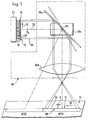
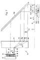
- the first simplest exemplary embodiment of a device according to the invention for generating an image 12 on an image surface 14 - for example a projection surface, on which the image is generated so as to be recognizable to a human eye - comprises a large number of semiconductor emitters 20 arranged in a row of lights 16 along a longitudinal direction 18 of the row of lights 16, each of which can be controlled individually by a common control 22 via individual control lines 24.
- the longitudinal direction 18 extends transversely to an optical axis 26 of a projection optical system, designated as a whole by 28, which images an exit spot 30 of each semiconductor emitter 20, from which radiation 32 generated by it emits, onto an image spot 34 of the image area 14, which is different from that Semiconductor emitter 20 generated radiation is then illuminated.
- the projection optics 28 is constructed in such a way that the exit spot 30 of each semiconductor emitter 20 is projected onto a single image spot 34 in the image area 14 at a specific point in time.
- the projection optics 28, as shown schematically in FIGS. 1 and 2 comprise a tilting mirror 28a, which can be pivoted about a tilting axis 28c by a pivoting drive 28b, and a lens 28d, which emits radiation 32 emerging from each semiconductor emitter 20 with a slight divergence illuminates the image spot 34 on the basis of the geometric image, the image spot 34 generally having an area which corresponds to a multiple of the exit spot 30.
- the image curvature is corrected either via a suitably shaped lens 28d or via a suitably controlled movement of the mirror in such a way that it does not fluctuate about the fixed tilt axis 28c, but rather the tilt axis also moves.
- the row of lights 16 consists of individual semiconductor emitters 30 arranged side by side in the longitudinal direction 18 and the projection optics 28 comprise the tilting mirror 28a and the simple lens 28d
- individual image spots 34 which lie side by side in a longitudinal direction 36 are formed on the image surface 14 form a total of a series of images 38.
- the projection optics 28 are preferably designed such that the individual image spots 34 of the image row 38 do not overlap in the direction of the longitudinal direction 36.
- An embodiment of the projection plane is particularly preferred, in which the image spots 34 follow one another or adjoin one another with their outer edges at a small distance A.
- image row 38 is composed of several sets 38S of adjacent image spots 34, the image spots in each set 38S immediately following one another and sets 38S in longitudinal direction 36 likewise immediately following one another , so that the adjacent image spots 34 of successive sets 38S are also at a distance A from one another, like adjacent image spots 34 within one of the sets 38S.
- the totality of the sets 38S of the image spots 34 thus results in the totality of the image spots 34 of the image row 38.
- the tilting mirror 28a can be tilted into different positions, so that, as shown for example in FIG. 1 with the solid position of the tilting mirror 28a, the set 38S1 of image spots 34 can be generated and following this, as shown in FIG. 1 by the broken line position of the tilting mirror 28a, the adjoining set 38S2.
- a corresponding tilting of the tilting mirror 28a about the tilting axis 28c is to be carried out by means of the swivel drive 28b, the swivel drive 28b being designed in such a way that after illumination of the image spots belonging to the set 38S1, it swivels rapidly into the position shown in broken lines for a time Ta1, while during the time Ta2, which is the same as the time Ta1 to illuminate the image spots 34 of the set 38S2.
- an image row 38 is constructed, for example, from ten sets 38S of image spots 34 and thus the tilting mirror 28a can also be pivoted into ten different positions, each of the sets 38S of image spots 34 being illuminated during the time period Ta, which is for all sentences 38S is the same size.
- an image row 38 of 1250 image spots 34 can be built up in that the light row 16 illuminates 10 adjacent sets 38S of image spots 34 in succession during an image construction cycle, the image construction cycles being repeated periodically.
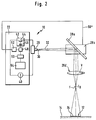
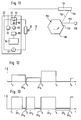
- the controller 22 In order to vary the brightness of the image spots 34 for the human eye observing the image 12, the controller 22, as shown in FIG. 2, comprises a current source 40 which is common to all semiconductor emitters 20 and which is used for each semiconductor emitter 20 provided current control block 42, which includes, for example, an FET transistor 44 as a current-controlling element, to the gate of which a capacitor 46 is connected as a memory element.
- This capacitor 46 of each current control block 42 can be charged with a specific charge via a control switch 48, the charge in the capacitor 46 determining the current through the FET transistor 44.
- the charge to be stored in the capacitor 46 is read out from a buffer 50 for each capacitor 46 of each current control block 42 by triggering the control switch 48 from the buffer 50, the buffer 50 preferably storing all control parameters and by triggering the control switch 48 all control parameters simultaneously the capacitors 46 of all current control blocks 42 are read.
- a trigger block 52 is provided for triggering the control switch 48.
- the buffer memory 50 has the current control parameters for the entire semiconductor emitter 20 the light row 16 has saved.
- the intensity of the radiation 32 emitted by it at the activation time t 1 by correspondingly charging the capacitor 46 of the corresponding one Control blocks 42 are set. The charge is then retained in the capacitor 46 so that the intensity of the radiation from the semiconductor emitter remains constant until the next activation time t 2. If the charge in the capacitor 46 is reduced at this time, this intensity is also maintained until the next activation time t 3. At the activation time t3, for example, the maximum intensity and thus the maximum charge is stored in the capacitor 46, while at the activation time t4 the minimum charge is stored, so that the semiconductor emitter 20 does not emit any radiation or radiation with the intensity 0 between the activation time t4 and t5.
- each individual semiconductor emitter 20 of the light row 16 can now be controlled individually, so that the image row 38 has image spots 34 of different intensities.
- the trigger block 52 is connected on the one hand via a line 56 to the swivel drive 28 and so synchronized with the swivel drive that, for example, at the time t 1 all capacitors 46 for all control blocks 42 are loaded with the values required for illuminating all the image spots 34 of the set 38S1 are and at time t2 the capacitors 46 are loaded so that they store the values for the image spots 34 of the set 38S2.
- the swivel drive 28b carries out the swivel movement from the solid position in FIG. 1 to the dash-dotted position at the greatest possible speed at the actuation time t 2.
- the time period Ta during which all the image spots 34 of the set 38S1 are illuminated in accordance with the brightness values stored in the image generator 54 thus corresponds to the time period between t 1 and t 2.
- This process is repeated during an image construction cycle until all sets 38S of image spots 34 of the image series 38 have been illuminated in succession during the period T a .
- control 22 In an alternative exemplary embodiment of the control 22 'according to the invention, shown in FIG. 4, those components which are identical to the control 22 are provided with the same reference numerals, so that the description of the control 22 is referred to in full in terms of its description.
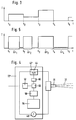
- each control block 42 ′ only comprises the control transistor 44, the gate of which is controlled by a pulse shaping stage 60 and which is only switched on and off between the state.
- the pulse shaper stage in turn stores the control parameters transmitted at the respective control time t and forms a control pulse of different lengths for the control transistor 44 according to the principle of pulse width modulation in accordance with the control parameters, so that the semiconductor emitter 20 is either switched on or off, but with a different length of time between the respective control times t, as shown in Fig. 5.
- the constant power values between the control points t1, t2, t3 and t4 are realized by pulse durations ⁇ t1, ⁇ t2, ⁇ t3 of different lengths, the semiconductor emitter emitting radiation 32 with the maximum power during the pulse durations ⁇ t1, ⁇ t2 and ⁇ t3.
- the effect is exploited that the human eye takes a temporal averaging when viewing the image spot 34 and thus the different pulse widths ⁇ t1, ⁇ t2 and ⁇ t3 convey the impression in the human eye, as if the power values shown in Fig. 3 during the entire period would exist between the control times t1, t2, t3 and t4.
- control 22 ′ is constructed identically to the control 22.
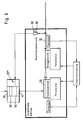
- a third exemplary embodiment of a controller 22 ′′ according to the invention, shown in FIG. 6, is constructed in such a way that each current control block converts the current of the respective semiconductor emitter 20 to the setpoint value stored in the intermediate memory 50 for each set 38S by means of a control circuit 56 regulates during the intended illumination time period Ta, the control circuit 56 measuring the amount of light of the radiation 32 emitted by each semiconductor emitter 20 via monitor photodiodes 60 combined into a monitor photodiode row 58 and driving the respective semiconductor emitter 20 in accordance with the measured value.
- the semiconductor emitter 20 can be driven with variable current, as shown in FIG. 3, so that the control circuit 56 regulates the magnitude of the current for each semiconductor emitter 20, or it is provided that the control circuit 56 regulates the time period ⁇ t while which each semiconductor emitter 20 is supplied with maximum current, the control circuit 56 switching off the current to the respective semiconductor emitter 20 when the quantity of light specified as the desired value in the buffer memory 50 is reached.
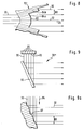
- the projection optics 28 comprise a spreading optics 70 which bring the radiation 32 from the semiconductor emitters to a greater distance, which in the simplest case, as shown in FIG. 7, comprises a substrate material 72 with a Refractive index n1, in which waveguides 74 are introduced, which have a refractive index n2, which is greater than n1.
- the radiation 32 coming from the respective exit spots 30 of the individual semiconductor emitters 20 is coupled into each of these waveguide tracks 74 in the region of one end 76 and is guided to a second end 78, from which the radiation 32 then emerges again.
- the first ends 76 of the waveguide tracks 74 lie at intervals which correspond to the distance between the exit spots 30 of the individual semiconductor emitters 20, so that the radiation 32 emerging from the exit spots 30 in the region of the first ends 76 into the waveguide tracks 74 enters and is guided from these to the second ends 78, which have exit spots 80 for the radiation 32, which are at an image spot spacing BR from one another.
- the radiation 32 emerging from the spreading optics 70 is then in turn imaged by the tilting mirror 28a onto the image row 38 in the image area 14, successive semiconductor emitters 20 being associated with individual image spots 34 in a position of the tilting mirror 28a, the spacing of which is a multiple of the distance A of the image spots 34 of the image series is 38.
- the image spots 34 illuminated by the light row 16 in a position of the tilting mirror 28a thereby form an image spot raster 38R, the same number of image spots 34 lying between individual image spots 34R1 of the image spot raster 38R1.
- the image spot grid 38R1 extends over the entire extent of the image row 38 in the longitudinal direction 36.
- the semiconductor emitter 20 which was previously assigned to one of the image spots 34R1, is assigned to the adjacent image spot 34R2, with the image spot 34R2 lying next to the image spots 34R1 of the image spot pattern 38R1 being assigned to each of the image spots 34R2
- Image spot grid 38R2 is formed whose image spots 34R2 in image row 38 are the image spots following image spots 34R1 of image spot screen 38R1.
- the semiconductor emitters 20 of the light row 16 are assigned to the adjacent image spots 34 to form an image spot grid 38R3, etc., until all the image spots 34 of the image row 38 were once part of an image spot grid 38R.
- the image construction cycle also takes that long, after which all image spots 34 of the image row 38 can be illuminated due to the comb-like assignment of individual image spots to a respective image spot grid and the advancement of the image spot grid to respectively adjacent image spots.
- the image construction cycles are repeated periodically in the same way as described in connection with the first exemplary embodiment of the device according to the invention, the tilt angles by which the tilt mirror 28a is to be pivoted being significantly smaller in this exemplary embodiment than in the first exemplary embodiment.
- a further exemplary embodiment of a spreading optics 70 'according to the invention, shown in detail in FIG. 8, comprises a multiplicity of prism elements 82, 84, wherein for example the prism element 82 is a prism element which is passed through unchanged by the radiation 32 and which is arranged coaxially to the optical axis 26, while the prism elements 84a, b, etc.
- the radiation 32 coming from the semiconductor emitters 20 is reflected by a reflection grating 90 which has reflection surfaces 92 which are at a distance in the direction of incidence 94 of the radiation 32 coming from the semiconductor emitters , which corresponds to the image spot spacing BR and has a distance perpendicular to the direction of incidence 94, which corresponds to the distance between the exit spots 30 of the semiconductor emitters, so that the radiation 32 coming from the exit spots 30 hits the reflection surfaces 92 directly and from them as radiation 32 with the desired Image spot spacing BR is reflected.
- a reflection grating 90 which has reflection surfaces 92 which are at a distance in the direction of incidence 94 of the radiation 32 coming from the semiconductor emitters , which corresponds to the image spot spacing BR and has a distance perpendicular to the direction of incidence 94, which corresponds to the distance between the exit spots 30 of the semiconductor emitters, so that the radiation 32 coming from the exit spots 30 hits the reflection surfaces 92 directly and from them as radiation 32 with the desired Image spot spacing BR is reflected.
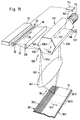
- the projection optics designated as a whole by 128, comprises, in addition to the elements described in connection with the first exemplary embodiment, such as tilting mirror 28a and pivoting drive 28b, a polygon mirror 130, which is arranged around a axis 132 parallel to the longitudinal direction 18 is driven in rotation by a drive 134.
- the polygon mirror 130 in turn has a multiplicity of polygon surfaces 136 arranged at equal angular intervals around the axis 132, one of the polygon surfaces 136 serving as a reflection surface.
- the row of lights 16 comprises a multiplicity of semiconductor emitters 20 which are arranged in succession in the longitudinal direction 18 and are likewise controlled by a control 22, 22 'or 22' '.
- the radiation 32 emerging from the exit spots 30 is first focused by a first focusing optics 138 on the polygon surface 136 in the reflecting position, and the radiation 140 reflected by the polygon surface 136 in the reflecting position is reflected by the tilting mirror 28a, intermediate focused and by a second focusing optics 142 the image area 14 is shown.
- the polygon surface 136 standing in the reflection position rotates about the axis 132 for as long as it is illuminated by the radiation 32, not only does an image row 38 arise on the image area 14, but a plurality of image rows 38 'are created which are arranged side by side in a transverse direction 144 running perpendicular to the longitudinal direction 36.
- a first row of images 38a ' is generated on the image surface 14 when the polygon surface 136 standing in the reflection position is acted upon by the radiation 32 at its foremost region 136a in the direction of rotation 146, and the last row of images 38b' is generated when the one standing in the reflection position Polygon surface 136 with its rearmost area 136b in the direction of rotation 146 of the polygon mirror is acted upon by radiation 32.
- each set of image spots 38S is initially imaged on all rows 38 ', that is to say from row 38a' to row 38b 'by one of the polygon surfaces 136.
- the tilting mirror 28a has moved so far that it illuminates the next image spot set 38S in all image rows 38 ', for example the image spot set 38S2 and maintains this illumination until it is now in Polygon surface 136 standing in the reflection position has projected this image spot set onto all image rows 38 '.
- the tilting mirror 28a has also moved on again, so that now the projection of the next set of image spots 38S3 onto the image rows 38 'takes place.
- the synchronization of the rotating polygon mirror 130 is also carried out with the respective control 22, 22 'or 22''via the connection to the trigger block 52, the tilting movement of the tilting mirror 28a being synchronized with the rotating movement of the polygon mirror 130 such that the tilting mirror 28a Maps row 16 of light to the next following set of image spots when the next following polygon surface 136 is in the reflection position.
- the drive 134 of the polygon mirror is preferably provided with an angle decoder and at the same time the swivel drive 28b of the tilting mirror 28a, so that simple synchronization via the respective control 22, 22 'or 22''is possible (FIG. 11).
- the tilting mirror 28a is driven by the swivel drive 28b in such a way that it quickly changes from one position to the other and this change takes approximately the same time as the change from one polygon surface to the next, so that the dead time is as short as possible.
- the time intervals in which the tilting mirror 28a moves and changes from one set to another are, for example for 125 semiconductor emitters and 100 image build-up cycles per second and 1250 image spots per image row, a maximum of 1 os, during which the polygon mirror 130 with a polygon area then forms a maximum of 1 os 136 each a set of image spots on all image rows 38 '.
- a further semiconductor emitter 148 is provided, as shown in FIG. 11, which illuminates, for example, the polygon surface 136 opposite the polygon surface 136 in the reflection position, the reflected radiation 152 being emitted strikes a detector designated as a whole by 154, which has one detector region 156 or a plurality of detector regions 156, the detector regions 156 having an extent which approximately corresponds to the cross section of the reflected radiation 152, so that when the reflected radiation 152 strikes the respective detector region 156 a precise angular position of the polygon mirror 130 is determined.
- the first detector region 156 is positioned such that when the reflected radiation 152 strikes it, the polygon surface 136 in the reflection position images the exit spots 30 of the semiconductor emitters 20 of the light row 16 in the respective image spot set 38S on the first image row 38a '.
- the second detector surface 156 is preferably arranged such that when the reflected radiation 152 strikes it, the polygon surface 136 in the reflection position images the exit spots 30 of the semiconductor emitters 20 of the light row 16 on the second image row 38 'and so on.
- the impact of the reflected radiation 152 on one of the detector areas 156 generates a signal in the detector 154, which is fed to the trigger block 52, for example, and causes the latter to trigger the control switch 48, if necessary with a corresponding time offset, so that at these control times t the control parameters for everyone Current control block 42 can be changed. It is thus possible to project image spots 34 with different intensity distribution onto each image line 38 'and thus to build up on the image area 14 a two-dimensional image extending in the longitudinal direction 36 and transverse direction 144 from the individual image spots 34 of the image row 38'.
- the control instants t are synchronized with the rotation of the polygon mirror 130 such that they preferably coincide with the instants in which the radiation 32 would strike an edge 160 lying between two polygon surfaces 136.
- the semiconductor emitters 20 can be switched off shortly before the respective activation time t by the fact that the maximum pulse width ⁇ t is shorter by the amount ⁇ t k than the period between successive activation times t, which preferably follow one another at constant time intervals.
- the drive 134 continuously rotates the polygon mirror 130 at a substantially stabilized speed.
- a stepper motor as drive 134 which can be brought into individual rotational positions in a controlled manner and thus does not rotate the polygon mirror 130 continuously, but rather rotates in such rotational positions that the polygon surface 136 in the reflection position successively has different angular positions with respect to the radiation 32 occupies, each individual angular position corresponding to the reflection of the exit spots 30 of the light row 16 in one of the picture rows 38 'and thus the picture rows 38' are illuminated for a defined time and then the polygon surface 136 standing in the reflecting position "jumps" into the next rotational position.
- a stepper motor as drive 134 which can be brought into individual rotational positions in a controlled manner and thus does not rotate the polygon mirror 130 continuously, but rather rotates in such rotational positions that the polygon surface 136 in the reflection position successively has different angular positions with respect to the radiation 32 occupies, each individual angular position corresponding to the reflection of the exit spots 30 of the light row 16 in one of the picture rows 38 'and thus the picture rows 38' are illuminate
- the trigger block 52 can then also be controlled in accordance with the control of the stepping motor, so that the detection of the rotational position of the polygon mirror 130 by means of the detector 154 can be dispensed with.
- a fourth exemplary embodiment of the device according to the invention, shown in FIG. 14, is based on the second exemplary embodiment and provides projection optics 128 which are designed in the same way as in the third exemplary embodiment, so that the spread optics 70 spread over the image spot spacing BR Radiation 32 now hits the tilting mirror 28a in the same way as in the second exemplary embodiment and illuminates the image spots 34 in each of the image rows 38 ', which are encompassed by the respective image spot grid 38R.
- one and the same image spot grid 38R is generated by the rotating polygon mirror 130 in all image rows 38 'and then to the next image spot screen 38R and this in turn in all image rows 38', that is to say from the image row 38a 'to Image series 38b '.
- the tilting mirror 28a can remain standing and, after the generation of the same image spot grid 38R in each of the image rows 38 ', can jump to the next tilt position in order to generate the next subsequent image spot grid 38R in all image rows 38', but it is also possible to slow the tilting mirror 28a to be pivoted continuously such that after one and the same image spot grid 38R has been generated in all image rows 38 ', the tilt is so large that the next image spot grid is already generated in the first image row 38a'.
- corresponding image spots 34 in the successive image rows 38 'do not lie on a straight line which is perpendicular to the longitudinal direction 36, but on a straight line which is at an angle ⁇ 90 ° to the longitudinal direction 36, the oblique position of the corresponding ones
- the time period for imaging each image spot raster 38R on all image rows 38 ' is a maximum of 1 ° s and then the system switches to the next image spot raster 38R.
- the tilting mirror 28a can be omitted if the polygon mirror 130 'does not have polygon surfaces 136' running parallel to the axis 132 ', but, as in Fig 16, all polygon areas 136 'successive to a first polygon area 136e' up to the last polygon area 136l ', to which the first polygon area 136e' is connected again, successively an inclination which changes by a constant angle value from polygon area 136 'to polygon area 136' have their center line 137 with respect to a parallel 133 to the axis 132, so that these polygon surfaces 136 ', each having a different inclination with respect to the axis 132, also take over the function of the tilting mirror 28a.
- the first polygon surface 136e ' is then in the reflection position when the light row 16 is to illuminate the image spot set 38S of the first image row 38a'. As long as the first reflection surface 136e 'is in the reflection position, the image spots 34 of the first image spot set 38S are generated in all image rows 38'.
- next polygon area 136 ' which is inclined so that it illuminates the third set of image spots 38S3 in direct connection to the second set of image spots 38S2.
- a sixth embodiment represents a further development of the fourth embodiment, but also with projection optics 128 ′ with a polygon mirror according to FIG. 17.
- the angles of the polygon surfaces 136 ' which change from polygon surface 136' to polygon surface 136 'are smaller with respect to axis 132, since when changing from the first image spot grid 38R1 to the second image spot grid 38R2, only one deviation has to occur such that in each case from the already generated image spots 34 to the next adjacent image spots 34 in each image row 38 ', while in the fifth embodiment the second image spot set 38S2 has to be shifted by a distance compared to the first image spot set 38S1, which multiplies the number of image spots in one image spot set 38S corresponds to the distance of the image spots A, while the shift in the sixth embodiment only has to be done by the distance of the image spots A.
- each row of lights 16 it is provided for each row of lights 16 that individual semiconductor emitters 20 sit next to one another in the longitudinal direction 18 and thus the row of lights 16 is formed by a single row of semiconductor emitters 20.
- each light row 216 has three rows 218, 220 and 222 of semiconductor emitters 20 which run parallel to one another, the row 218 being composed of semiconductor emitters 20R that emit red light, the row 220 is composed of semiconductor emitters 20G that emit green light, and the row 222 is composed of semiconductor emitters 20B that emit blue light.
- the projection optics 228 are constructed such that a respective semiconductor emitter 20R, a semiconductor emitter 20G and a semiconductor emitter 20B illuminate an image spot 234, in the simplest case it being provided that the partial image spots 236B, 236G and 20B generated by each of the semiconductor emitters 20R, 20G and 236R do not lie congruently one above the other, but do not overlap or only partially overlap, for example.
- a projection optics 228 intermediate focusing of the radiation 32 onto the polygon mirror 130 by means of the first focusing optics 138 can be dispensed with.
- the projection optics 228 are configured identically to the projection optics 128 of the fifth or sixth exemplary embodiment, so that reference is made here to details.
- the rows 218, 220 and 222 of the semiconductor emitters 20R, 20G and 20B are also controlled analogously to the options described in connection with the first exemplary embodiment, but for each of the Rows 218, 220 and 222 a buffer 50 and for each semiconductor emitter 20 a current control block 42 is required, but the control is carried out in such a way that at a control time t the control parameters for the semiconductor emitters 20R, 20G and 20B of all three rows 218, 220 and 222 simultaneously can be read from the buffer.
- the wavelengths of the semiconductor emitters 20R, 20G and 20B and the possible maximum intensities are selected such that all colors, in particular white, can be generated by color mixing in the image spots 234 for the human eye.
- the image generator 54 now generates three control parameters for each image spot 234 for each of the semiconductor emitters 20R, 20G and 20B illuminating this image spot 234.
- the three rows 218, 220 and 222 each comprising the semiconductor emitters 20R, 20G and 20B, are also provided. The control of the same takes place as described in connection with the third embodiment.
- the projection optics 328 between the light row 216 and the polygon mirror 130 each comprise two sets of mirrors 330 and 332 in order to combine the radiation 32R from the semiconductor emitters 20R, the radiation 32G from the semiconductor emitters 20G and the radiation 32B from the semiconductor emitters 20B.
- the first set of mirrors 330 comprises a dichroic mirror 333 arranged in the beam path of the radiation 32R and a mirror 336 reflecting the radiation 32G on the dichroic mirror.
- the second set of mirrors 332 comprises a dichroic mirror 338 arranged in the beam path of the radiation 32R and one the radiation 32B on the dichroic mirror 338 reflective mirror 340.
- the two dichroic mirrors 333 and 338 thus combine the radiation 32R, 32G and 32B to form radiation 32V, which impinges on the polygon mirror 130 designed in accordance with the fifth or sixth exemplary embodiment and by the latter in the manner already described in connection with the second exemplary embodiment Image area 14 is reflected.
- the advantage of this projection optics 328 can be seen in the fact that, in this exemplary embodiment, the partial image spots 336, produced by imaging the exit spots 30 of the semiconductor emitters 20R, 20G and 20B, can be superimposed essentially congruently in each image spot 334.
- the semiconductor emitters preferably comprise semiconductor lasers designed as so-called edge emitters, as shown schematically in FIG. 20.
- Such edge emitters consist of a multiplicity of semiconductor layers 800, between which a laser-active layer 802 is arranged.
- the laser radiation 806 emerges from this laser-active layer in the region of an exit spot 804.
- Such an edge emitter is operated by supplying current via two current connections 808 and 810, the current flowing essentially perpendicular to the layers 800 and 802.
- Embodiments of such edge emitters can be found in the magazine Laser Focus World, July 1993, Vol. 29, No. 7, pages 83 to 92 described in detail.
- edge emitters can be seen in the fact that they can be produced in a simple manner side by side as a so-called array on a substrate.
- edge emitters it is possible to provide semiconductor lasers in the form of so-called vertical emitters, shown in FIG. 21, as radiation sources, with such vertical emitters also having a laser-active layer 902 between a plurality of semiconductor layers 900 and additional laser-active layer 902 on both sides , Layers 904 serving as Bragg reflectors are provided.
- the resulting laser radiation does not propagate parallel to the active layer 802 as in the case of the edge emitter, but perpendicular to the active layer 902, passes through the substrate 910 and preferably exits perpendicular to the plane of the substrate 910.
- Vertical emitters have the advantage that the resulting laser radiation 906 has an approximately circular cross section and can therefore be coupled to other optical elements, for example fiber-optic elements, in a simple manner.
- the following laser materials are preferably used as laser materials for the generation of radiation in the visible range with different colors: Al x Ga y In 1-xy P on GaAs for 610-690 nm red Zn 1-x Mg x S 1-y Se y on GaAs for 450-550 nm blue green Al x Ga y In 1-xy N For UV - red
- Such materials would be, for example A1 x Ga 1-x As on GaAs (780-880nm) for blue In x Ga 1-x As on GaAs (880-1100nm) for blue, green In 1-x Ga x As y P 1-y on InP (1100-1600nm) for red.
- An embodiment of such semiconductor emitters 20 'doubling the wavelength of the radiation from the radiation source, shown in FIGS. 22 and 23 in the form of a section from the light row 820, comprises an array 822 of edge emitters 826 arranged on a common substrate 824, which are characterized by special emitters laser-active layers arranged on the common substrate 824 are formed6 and each have as laser-active layer 802 a strip-shaped region 828 of a continuous layer 830 arranged on the common substrate 824.
- Each of the semiconductor lasers 826 serving as a radiation source is assigned a frequency doubler 832, each of which comprises a waveguide structure 834 in which a frequency-doubled medium is arranged as a waveguide channel 836.
- the waveguide structure 834 guides the radiation generated by the respective semiconductor laser 826 in such a narrow cross section that a power density of at least 105W / cm2, preferably at least 106W / cm2, which is required for efficient frequency doubling in the frequency-doubling medium, is achieved.
- all frequency doublers 832 are also arranged on a common substrate 838 in the form of an array 840.
- the waveguide structure 834 is formed by a base layer 842 and a cover layer 844, which represent upper and lower walls of the waveguide channel 834, and spaced-apart strip areas 846 and 848 of an intermediate layer 850, which form side walls of the waveguide channel 834 and a strip area 852 des Include the intermediate layer 850 between them, which forms the frequency doubling medium 836 serving as the waveguide core.
- the base layer 842, the top layer 844 and the strip-shaped regions 846 and 848 of the intermediate layer 850 have a refractive index which is smaller than the refractive index of the strip-shaped region 852, so that at the boundaries between the strip-shaped region 852 and the layers 842 and 844 as well the strip-shaped regions 846 and 848 there is a total reflection of the radiation and thus the guidance of the radiation in the waveguide structure 834.
- the extension of the waveguide structures 834 transverse to their longitudinal direction 854 is expediently chosen to be approximately the same size as the extension of the laser-active regions 828 in the direction of propagation 856 of the laser radiation.
- the fundamental wave that is to say the radiation coming from the corresponding semiconductor laser 826
- the doubled radiation must remain in phase the entire way through the frequency doubling medium. This is optimally achieved when working with an uncritical or non-critical phase adjustment in which the angle is 0 or 90 °.
- the respective material is preferably adapted to the corresponding wavelength by varying the temperature, so that, for example, the substrate 838 is seated on a temperature control device 860, with which the entire array 840 of frequency doublers 832 can be brought to an optimum temperature for the uncritical phase adjustment this is durable.
- the temperature control device 860 is preferably provided with a control, by means of which a predeterminable temperature can be set and maintained by readjustment.
- the direction of the crystal in the frequency-doubling medium 836 is expediently predetermined by the orientation of the substrate 838, which is oriented such that the optical axis of the substrate is oriented in the desired direction to the longitudinal direction 854 of the waveguide channel 834. If the layers 842, 844 and 850 made of the same base material, possibly with different dopings, are grown on this substrate 838, these layers have the same orientation of the optical axes as the substrate 838 and consequently the position of the optical axes is also frequency doubling Medium 836 can be specified.
- phase adaptation is achieved in that in the frequency-doubling medium 836' domains 870 and 872 follow one another, in which the non-linear ones Coefficients of the frequency doubling medium 836 each have opposite signs.
- An extension L of the domains 870 and 872 in the longitudinal direction 854 of the waveguide channels 834 is to be coordinated in such a way that it corresponds to the coherence length.
- the array 840 ' is of the same design as the array 840, so that full reference can be made to the explanations in this regard and the same reference numerals are used for the same elements.
- a crystal of lithium niobate for the wavelengths green and red is preferably used as the frequency-doubling medium and a crystal of potassium niobate for the wavelength blue.
- the waveguide structure 834 is produced in that the material surrounding the waveguide core is lithium niobate or potassium niobate, which has additionally been doped with magnesium or other elements which lower the refractive index.
- an array 922 of semiconductor lasers 926 designed as vertical emitters is used.
- the radiation 928 from these semiconductor emitters is focused by focusing elements 930 onto frequency doublers 932, which are likewise arranged in an array 940 on a common substrate and are constructed and constructed in the same way as the array 840, so that reference can be made in full to the explanations in this regard .
- the focusing optics 930 are not designed as lens optics, but rather as gradient index lenses, which are used as a block between the respective semiconductor lasers 926 and the corresponding frequency doublers 932 and, due to the gradient index, focus the radiation 928 onto the waveguide channels 934.
- the end of the frequency doubler 932 expansion optics 970 are preferably arranged, which are also gradient index lenses that generate a substantially parallel beam 972.
- an array 1022 of individual semiconductor lasers 1026 designed as edge emitters is arranged on the common substrate 1024, individual laser-active layers being formed on the common substrate 1024, each as laser-active layer 1002 have a strip-shaped area on a continuous layer arranged on the common substrate 1024.
- the substrate 1024 sits on a cooling element 1050 and is thermally coupled to a temperature sensor 1052, which regulates the cooling element 1050 to a constant temperature via a temperature control 1054, so that ultimately the substrate 1024 of the semiconductor emitter 1026 also has a constant temperature.
- a cooling element 1056 is provided for the frequency doubler 1032, the base layer 1042 being cooled by the cooling element 1056. Furthermore, a temperature sensor 1058 is coupled to this base layer 1042, which also again enables the temperature control 1054 to set a constant temperature of the base layer 1042, so that ultimately a constant temperature for the frequency-doubling medium 1036 is also present in the waveguide channel.
- the exit spots 1060 of the edge emitters 1026 are preferably imaged via a lens system 1062 onto the entrance spots 1064 of the waveguide structure and their exit spots 1066 are in turn shaped via a lens system 1068 into parallel radiation 32 leaving the respective semiconductor emitter 1020, the radiation being a window 1070 of a housing 1072 penetrates, which in turn includes both the array 1022 and the entirety of the waveguide structures 1034 with the cooling elements 1050 and 1056 and the temperature sensors 1052 and 1058 and the lenses 1062 and 1066.
- a beam splitter 1074 is provided in front of the exit window 1070, which reflects part of the radiation passing through the outer window 1070 onto a row of monitor photodiodes 1076, which is likewise arranged in the housing 1072 and has a monitor photodiode for each of the edge emitters 1026. All monitor photodiodes are coupled to the controller 22 ', which has already been described in detail in connection with the third exemplary embodiment of the controller according to the invention according to FIG. 6.
- the lens systems 1062 and 1068 each comprise the radiation-forming microlens systems, which are likewise arranged on a substrate. Furthermore, the waveguide structure of the frequency doubler 1032 is again shown enlarged in FIG. 27.
Abstract
Description
Die Erfindung betrifft eine Vorrichtung zur Erzeugung eines insbesondere für ein menschliches Auge sichtbaren Bildes in einer Bildfläche, umfassend eine Strahlungsquelle, welche über eine Projektionsoptik ein Bild dadurch erzeugt, daß sie während eines Bildaufbauzyklus mindestens eine Bildreihe durch Ausleuchten einzelner nebeneinander liegender Bildflecken aufbaut und den Bildaufbauzyklus periodisch wiederholt.The invention relates to a device for generating an image, in particular visible to a human eye, in an image area, comprising a radiation source which generates an image via projection optics in that it builds up at least one row of images by illuminating individual image spots lying next to one another during an image construction cycle and the image construction cycle repeated periodically.
Die erfindungsgemäßen Vorrichtungen dienen beispielsweise dazu, nicht nur statische sondern auch bewegte Bilder, wie beispielsweise Fernsehbilder, in Großformat und gegebenenfalls auch mehrfarbig zu erzeugen.The devices according to the invention serve, for example, to generate not only static but also moving images, such as television images, in large format and optionally also in multicolor.
Eine derartige Vorrichtung ist beispielsweise aus der DE-A-23 41 705 bekannt, wobei bei dieser Art von Vorrichtungen die Bilderzeugung mit Gaslasern erfolgt und ein Laserstrahl eines Gaslasers über die Projektionsoptik zur Erzeugung eines für das menschliche Auge als Ganzes erkennbaren Bildes aus einzelnen Bildpunkten bewegt wird.Such a device is known, for example, from DE-A-23 41 705, with this type of device the image formation using gas lasers and a laser beam of a gas laser being moved from the projection optics to produce an image which can be recognized as a whole by the human eye from individual pixels becomes.
Die Verwendung derartiger Gaslaser zur Bilderzeugung erfordert einen großen apparativen Aufwand zur Erzeugung des Laserstrahls und außerdem einen großen Aufwand bei der Projektionsoptik, um den Laserstrahl definiert abzulenken.The use of such gas lasers for image generation requires a large outlay in terms of apparatus for generating the laser beam and also a large outlay in projection optics in order to deflect the laser beam in a defined manner.
Der Erfindung liegt daher die Aufgabe zugrunde, eine Vorrichtung der gattungsgemäßen Art derart zu verbessern, daß die Bilderzeugung möglichst einfach und daher auch kostengünstig möglich ist.The invention is therefore based on the object of improving a device of the generic type in such a way that image generation is as simple as possible and therefore also possible at low cost.
Diese Aufgabe wird bei einer Vorrichtung der eingangs beschriebenen Art erfindungsgemäß dadurch gelöst, daß zur Ausleuchtung der Bildflecken der Bildreihe eine eine Vielzahl von Halbleiteremittern umfassende Leuchtreihe vorgesehen ist, daß die Projektionsoptik jeden Austrittsfleck für die Strahlung jedes Halbleiteremitters mindestens einem der Bildflecken zuordnet und daß die Projektionsoptik die Austrittsflecken aller Halbleiteremitter der Leuchtreihe gleichzeitig auf die diesen zugeordneten Bildflecken abbildet.This object is achieved according to the invention in a device of the type described at the outset in that a row of light comprising a plurality of semiconductor emitters is provided for illuminating the image spots in the image row, in that the projection optics associate each exit spot for the radiation from each semiconductor emitter with at least one of the image spots and in that the projection optics maps the exit spots of all semiconductor emitters of the light row simultaneously onto the image spots assigned to them.
Der Vorteil der erfindungsgemäßen Lösung ist darin zu sehen, daß einerseits die Halbleiteremitter eine einfach aufgebaute und zu betreibende Strahlungsquelle darstellen, und daß andererseits die vorgesehene Vielzahl von Halbleiteremittern der Leuchtreihe die Projektionsoptik insoweit vereinfacht, als diese alle Halbleiteremitter der Leuchtreihe gleichzeitig auf die diesen zugeordneten Bildflecken abbilden kann, so daß, ausgehend von beispielsweise 100 Bildaufbauzyklen pro Sekunde, an die Projektionsoptik geringere Anforderungen gestellt werden.The advantage of the solution according to the invention can be seen in the fact that, on the one hand, the semiconductor emitters represent a simply constructed and operable radiation source, and, on the other hand, that the provided plurality of semiconductor emitters of the light row simplify the projection optics insofar as they simultaneously all semiconductor emitters of the light row onto the image spots assigned to them image, so that, starting from, for example, 100 image build-up cycles per second, less demands are made on the projection optics.
Als besonders vorteilhaft erweist sich diese Lösung, wenn man davon ausgeht, daß das Bild, um als Ganzes für das menschliche Auge sichtbar zu sein, mindestens in dem bei Fernsehgeräten üblichen Zeitraum aufgebaut sein muß und sich mindestens mit bei Fernsehgeräten üblichen Wiederholfrequenzen wiederholen muß.This solution proves to be particularly advantageous if it is assumed that the image, in order to be visible as a whole to the human eye, must be built up at least in the time period customary for television sets and must be repeated at least with the repetition frequencies customary for television sets.
Dabei besteht die Möglichkeit, beispielsweise die Vielzahl der Halbleiteremitter so zu wählen, daß zu einem Zeitpunkt die Projektionsoptik einen Teil der Bildflecken einer Bildreihe ausleuchtet und zu einem späteren Zeitpunkt einen anderen Teil.It is possible, for example, to select the multiplicity of semiconductor emitters in such a way that the projection optics illuminates part of the image spots of an image row at one point in time and another part at a later point in time.
Eine Reihe im Sinne der Erfindung kann horizontal oder vertikal verlaufen.A row in the sense of the invention can run horizontally or vertically.
Rein theoretisch wäre es denkbar, mit mehreren jeweils Licht derselben Wellenlänge aussendenden Halbleiteremittern einen Bildfleck auszuleuchten. Besonders ökonomisch ist jedoch die erfindungsgemäße Vorrichtung dann, wenn die Projektionsoptik - insbesondere für die bei derselben Wellenlänge strahlenden Halbleiteremitter - während des Bildaufbauzyklus unterschiedliche Austrittsflecken auch unterschiedlichen Bildflecken der Bildreihe zuordnet.In theory, it would be conceivable to illuminate an image spot with several semiconductor emitters each emitting light of the same wavelength. However, the device according to the invention is particularly economical if the projection optics - in particular for the semiconductor emitters radiating at the same wavelength - assign different exit spots to different image spots of the image row during the image construction cycle.
Ferner wäre es auch denkbar, die Bildflecken den Austrittsflecken bei unterschiedlichen Bildaufbauzyklen unterschiedlich zuzuordnen. Besonders einfach ist jedoch die Projektionsoptik dann aufgebaut, wenn während jedes Bildaufbauzyklus die selben Austrittsflecken den selben Bildflecken der Bildreihe zugeordnet sind.Furthermore, it would also be conceivable to assign the image spots to the exit spots differently in the case of different image construction cycles. However, the projection optics are particularly simple if the same exit spots are assigned to the same image spots of the image row during each image construction cycle.
Die Vielzahl der Halbleiteremitter könnte so gewählt werden, daß jedem Bildfleck ein Halbleiteremitter zugeordnet ist. Um jedoch die Zahl der Halbleiteremitter, die auf kleinstem Raum nebeneinander angeordnet sind, zu begrenzen, ist es jedoch vorteilhaft, wenn die Vielzahl der Halbleiteremitter kleiner ist als die Gesamtzahl der Bildflecken der Bildreihe und wenn die Projektionsoptik die Austrittsflecken während des Bildaufbauzyklus zu aufeinanderfolgenden Zeitpunkten auf verschiedene Bildfleckenserien der Bildreihe abbildet. Das heißt insbesondere, daß die Vielzahl der Halbleiteremitter während des Bildaufbauzyklus zunächst zur Ausleuchtung eines Teils der Bildflecken der Bildreihe dient, in diesem Fall als Bildfleckenserie bezeichnet, und daß während des Bildaufbauzyklus die komplette Ausleuchtung der Bildreihe dadurch erfolgt, daß die einzelnen Bildfleckenserien zeitlich nacheinander ausgeleuchtet werden, wobei, wenn dies schnell erfolgt, das menschliche Auge die Bildreihe als kontinuierlich ausgeleuchtet sieht.The plurality of semiconductor emitters could be chosen so that a semiconductor emitter is assigned to each image spot. However, in order to limit the number of semiconductor emitters that are arranged side by side in the smallest space, However, it is advantageous if the plurality of semiconductor emitters is smaller than the total number of image spots in the image row and if the projection optics images the exit spots on different image spot series of the image row at successive times during the image construction cycle. This means in particular that the large number of semiconductor emitters during the image build-up cycle initially serves to illuminate part of the image spots in the image series, in this case referred to as image spot series, and that during the image build-up cycle the complete illumination of the image series takes place in that the individual image spot series are illuminated sequentially where, if this happens quickly, the human eye sees the series of images as continuously illuminated.
Hinsichtlich der Zusammenstellung der eine Bildfleckenserie bildenden Bildflecken sind unterschiedliche Möglichkeiten denkbar. So sieht ein vorteilhaftes Ausführungsbeispiel vor, daß die Projektionsoptik die Austrittsflecken der Leuchtreihe während des Bildaufbauzyklus zu jedem der aufeinanderfolgenden Zeitpunkte jeweils auf eine Bildfleckenserie der Bildreihe abbildet und daß die Bildfleckenserie durch einen Satz unmittelbar nebeneinanderliegender Bildflecken gebildet ist. Das heißt, daß jeweils nebeneinander liegende Bildflecken zu einem Satz zusammengefaßt werden und daß durch Ausleuchten mehrerer Sätze nacheinander während des Bildaufbauzyklus die Gesamtausleuchtung der Bildreihe erfolgt.With regard to the composition of the image spots forming a series of image spots, different possibilities are conceivable. An advantageous exemplary embodiment provides that the projection optics images the exit spots of the light row during the image build-up cycle at each of the successive times in each case on an image spot series of the image row and that the image spot series is formed by a set of image spots lying directly next to one another. This means that adjacent image spots are combined to form a sentence and that by illuminating several sentences in succession during the image construction cycle, the entire illumination of the image series is carried out.
Prinzipiell könnte dies dadurch erfolgen, daß ein Bildfleck auch Bestandteil mehrerer Sätze ist, so daß eine Mehrfachausleuchtung jedes Bildfleckens während eines Bildaufbauzyklus erfolgt. Besonders einfach ist es jedoch, wenn jeder Bildfleck der Bildreihe jeweils von einem Satz von Bildflecken umfaßt ist, so daß nur einmal im Zusammenhang mit der Ausleuchtung eines Satzes die Ausleuchtung eines Bildfleckens der Bildreihe erfolgt.In principle, this could be done in that an image spot is also part of several sets, so that multiple illumination of each image spot takes place during an image construction cycle. However, it is particularly simple if each image spot in the image row is surrounded by a set of image spots, so that only one image spot of the image row is illuminated in connection with the illumination of a set.
Ferner ist es prinzipiell denkbar, die Sätze von Bildflecken so anzuordnen, daß diese unterschiedliche, nicht unbedingt miteinander korrelierte Abschnitte der Bildreihe umfassen.Furthermore, it is in principle conceivable to arrange the sets of image spots in such a way that they comprise different, not necessarily correlated sections of the image row.
Besonders vorteilhaft ist es jedoch, wenn die Projektionsoptik die Sätze von Bildflecken so in die Bildreihe legt, daß zeitlich aufeinanderfolgende Sätze von Bildflecken unmittelbar aufeinander anschließen.However, it is particularly advantageous if the projection optics place the sets of image spots in the image row in such a way that temporally successive sets of image spots immediately follow one another.
Alternativ zum Ausleuchten der Bildreihe in Form von Sätzen von Bildflecken ist vorgesehen, daß die Projektionsoptik nebeneinander liegende Austrittsflecken der Leuchtreihe auf eine als Bildfleckenraster ausgebildete Bildfleckenserie mit einem Bildfleckenrasterabstand abbildet, der jeweils ein bestimmtes Vielfaches des Abstandes nebeneinander liegender Bildflecken des Bildes beträgt. Vorzugsweise ist dies ein ganzzahliges Vielfaches des Abstandes nebeneinanderliegender Bildflecken des Bildes.As an alternative to illuminating the image row in the form of sets of image spots, it is provided that the projection optics map adjacent exit spots of the light row onto an image spot series designed as an image spot grid with an image spot grid spacing which is in each case a certain multiple of the distance between adjacent image spots of the image. This is preferably an integer multiple of the distance between adjacent image spots of the image.
Um hierzu die Strahlung nebeneinanderliegender Halbleiteremitter auf einen Abstand zu bringen, welcher nach Abbildung durch die Projektionsoptik dem Bildfleckenrasterabstand in der Bildreihe entspricht, ist vorteilhafterweise vorgesehen, daß die Vorrichtung eine Spreizoptik umfaßt, welche den Abstand zwischen nebeneinander liegenden Austrittsflecken der Leuchtreihe auf einen Rasterabstand abbildet, der nach Abbildung durch die Projektionsoptik in dem Bild den Bildfleckenrasterabstand ergibt.In order to bring the radiation of adjacent semiconductor emitters to a distance for this purpose, which corresponds to the image spot grid spacing in the image row after being imaged by the projection optics, it is advantageously provided that the device comprises a spreading optic which maps the distance between adjacent exit spots of the light row to a grid spacing, which results in the image spot grid spacing in the image by the projection optics.
Diese Spreizoptik kann in unterschiedlichster Art und Weise ausgebildet sein.This spreading optics can be designed in a wide variety of ways.
Vorzugsweise ist vorgesehen, daß die Spreizoptik den Abstand zwischen nebeneinanderliegenden Austrittsflecken der Leuchtreihe auf den Rasterabstand vergrößert.It is preferably provided that the spreading optics increase the distance between adjacent exit spots of the row of lights to the grid spacing.
Hierzu ist vorzugsweise vorgesehen, daß die Spreizoptik die aus den Austrittsflecken austretenden Strahlenbündel auf parallele im Rasterabstand zueinander verlaufende Strahlenbündel abbildet.For this purpose, it is preferably provided that the spreading optics image the beams of rays emerging from the exit spots onto parallel beams of rays running at a grid spacing from one another.
Die Spreizoptik kann selbst aus unterschiedlichsten Elementen aufgebaut sein. So sieht ein vorteilhaftes Ausführungsbeispiel vor, daß die Spreizoptik mehrere Prismenelemente umfaßt, in welche die aus der Leuchtreihe kommende Strahlung der einzelnen Halbleiteremitter eintritt, und daß die Prismenelemente aus der Spreizoptik austretende Strahlenbündel erzeugen, welche den Rasterabstand voneinander aufweisen.The spreading optic can itself be constructed from a wide variety of elements. An advantageous exemplary embodiment provides that the spreading optics comprise a plurality of prism elements into which the radiation from the individual semiconductor emitters comes from the row of lights, and that the prismatic elements produce beams of rays emerging from the spreading optics which are spaced apart from one another.
Alternativ zum Vorsehen von Prismenelementen ist vorgesehen, daß die Spreizoptik ein Reflexionsgitter umfaßt, dessen Reflexionsflächen in Einfallsrichtung der von den Halbleiteremittern kommenden Strahlung den bestimmten Rasterabstand aufweisen und somit die Strahlung bereits in dem Rasterabstand reflektieren.As an alternative to the provision of prism elements, it is provided that the spreading optics comprise a reflection grating, the reflection surfaces of which have the determined grid spacing in the direction of incidence of the radiation coming from the semiconductor emitters and thus reflect the radiation already at the grid spacing.
Eine weitere alternative Möglichkeit, die Spreizoptik aufzubauen, sieht vor, daß die Spreizoptik für jeden der Austrittsflecken einen Lichtleiter umfaßt, daß in die Lichtleiter an einem Ende die Strahlung aus den jeweiligen Austrittsflecken der Halbleiteremitter eintritt und daß die Lichtleiter mit dem anderen Ende in dem vorbestimmten Rasterabstand angeordnete Lichtleiteraustrittsflecken festlegen.A further alternative possibility for constructing the spreading optics provides that the spreading optics comprise a light guide for each of the exit spots, that the radiation from the respective exit spots of the semiconductor emitters enters the light guides and that the light guides with the other end in the predetermined one Define the grid spacing of the light guide exit spots.
Die Spreizoptik kann im einfachsten Fall so aufgebaut sein, daß als Lichtleiter auf einem Substrat angeordnete Lichtleiterpfade vorgesehen sind.In the simplest case, the spreading optics can be constructed such that light guide paths arranged on a substrate are provided as light guides.
Hinsichtlich der Projektionsoptik wurden bislang keine näheren Angaben gemacht. So wäre es beispielsweise möglich, daß die Projektionsoptik in statistisch sich ändernden Intervallen während des Bildaufbauzyklus der Bildreihe die Austrittsflecken auf die verschiedenen Bildfleckenserien abbildet. Besonders vorteilhaft ist es jedoch, um eine optimale Ausleuchtung der einzelnen Bildflecken bei möglichst geringer Leistung der Halbleiteremitter zu erreichen, wenn die Projektionsoptik zur Erzeugung der Bildreihe die Austrittsflecken der Leuchtreihe sukzessive nacheinander auf verschiedene Bildfleckenserien abbildet und somit die Totzeiten zwischen der Ausleuchtung einzelner Bildfleckenserien möglichst gering gehalten werden.No details have so far been given with regard to the projection optics. For example, it would be possible for the projection optics to map the exit spots onto the different image spot series at statistically changing intervals during the image construction cycle of the image row. However, in order to achieve optimal illumination of the individual image spots with the lowest possible power of the semiconductor emitters, it is particularly advantageous if the projection optics for generating the image row successively images the exit spots of the light row on different image spot series and thus the dead times between the illumination of individual image spot series are as short as possible being held.
Dies läßt sich konstruktiv am einfachsten dadurch realisieren, daß die Projektionsoptik ein strahlumlenkendes Element umfaßt, welches die Leuchtreihe in die aufeinanderfolgenden Bildfleckenserien abbildet.The easiest way to achieve this in terms of design is for the projection optics to comprise a beam-deflecting element which reproduces the row of lights in the successive series of image spots.
Das strahlumlenkende Element kann dabei in unterschiedlichster Art und Weise ausgebildet sein. Dies kann beispielsweise ein Prisma oder eine Linse sein, welches bewegbar ist. Besonders vorteilhaft ist es jedoch, wenn das strahlumlenkende Element ein bewegbares Reflexionselement ist.The beam deflecting element can be designed in a wide variety of ways. This can be a prism or a lens, for example, which is movable. However, it is particularly advantageous if the beam-deflecting element is a movable reflection element.
Hierzu ist konstruktiv in einfacher Weise vorgesehen, daß das Reflexionselement in definierte Winkelpositionen bewegbar ist, die die Leuchtreihe in jeweils eine der Bildfleckenserien abbilden.For this purpose, it is structurally provided in a simple manner that the reflection element can be moved into defined angular positions which depict the row of lights in each of one of the image spot series.
Am einfachsten läßt sich dies konstruktiv dadurch lösen, daß das strahlumlenkende Element durch einen um eine Achse verschwenkbaren Spiegel gebildet ist.The simplest way to solve this constructively is that the beam-deflecting element is formed by a mirror pivotable about an axis.
Dieser Spiegel kann so aufgebaut sein, daß er sich während eines Bildaufbauzyklus kontinuierlich bewegt.This mirror can be constructed to move continuously during an image build cycle.
Alternativ dazu ist vorgesehen, daß der Spiegel während des Bildaufbauzyklus einzelne definierte Stellungen durchläuft, das heißt in einzelne definierte Stellungen gebracht wird, beispielsweise durch eine Schrittmotoransteuerung oder eine Ansteuerung mittels Piezoelementen oder ähnliches.As an alternative to this, it is provided that the mirror passes through individual defined positions during the image build-up cycle, that is to say is brought into individually defined positions, for example by means of a stepper motor control or control by means of piezo elements or the like.
Bislang wurde bei der Beschreibung der erfindungsgemäßen Lösung lediglich vom Aufbau einer Bildreihe aus unterschiedlichen Bildfleckenserien ausgegangen, da dies der einfachste Fall der erfindungsgemäßen Lösung ist. Besonders vorteilhaft ist es jedoch, wenn die Projektionsoptik während des Bildaufbauzyklus das Bild aus mehreren nebeneinanderliegenden Bildreihen aufbaut und somit ein zweidimensionales Bild, wie beispielsweise ein Fernsehbild, aufbaut.So far, the description of the solution according to the invention was based solely on the construction of an image row from different image spot series, since this is the simplest case of the solution according to the invention. However, it is particularly advantageous if the projection optics builds up the image from a number of adjacent image rows during the image construction cycle and thus builds up a two-dimensional image, such as a television image.
Besonders zweckmäßig ist es hierfür, wenn die Projektionsoptik die Bildflecken einer Bildfleckenserie in jeder Bildreihe erzeugt und dann die nächste Bildfleckenserie in jeder Bildreihe erzeugt, so daß zuerst in jeder Bildreihe die eine Bildfleckenserie erzeugt wird und dann in jeder Bildreihe die nächste Bildfleckenserie.It is particularly expedient for this if the projection optics generates the image spots of one image spot series in each image row and then generates the next image spot series in each image row, so that first the one image spot series is generated in each image row and then the next image spot series in each image row.
Vorzugsweise ist hierzu vorgesehen, daß die Projektionsoptik ein strahlumlenkendes Element umfaßt, welches die Bildfleckenserien in aufeinanderfolgenden Bildreihen erzeugt, wobei das strahlumlenkende Element insbesondere ein bewegbares Reflexionselement oder eine bewegbare Linse oder ein bewegbares Prisma ist.It is preferably provided for this that the projection optics comprise a beam-deflecting element which generates the image spot series in successive image rows, the beam-deflecting element being in particular a movable reflection element or a movable lens or a movable prism.
Zweckmäßigerweise ist das strahlumlenkende Element in definierte Positionen bewegbar, die die Bildfleckenserien in Jeder der Bildreihen erzeugen.The beam-deflecting element can expediently be moved into defined positions which generate the image spot series in each of the image rows.
Eine besonders vorteilhafte Lösung sieht vor, daß das strahlumlenkende Element durch einen um eine Drehachse rotierenden Polygonspiegel gebildet ist.A particularly advantageous solution provides that the beam-deflecting element is formed by a polygon mirror rotating about an axis of rotation.
Vorzugsweise ist der Polygonspiegel dabei so aufgebaut, daß er mit jeder Polygonfläche die von der Leuchtreihe kommende Strahlung so reflektiert, daß diese die Zahl der nebeneinanderliegenden Bildreihen durch Drehung in einem bestimmten Winkelbereich durchläuft und dann zur nächsten Polygonfläche übergeht.The polygon mirror is preferably constructed in such a way that with each polygon surface it reflects the radiation coming from the light row in such a way that it passes through the number of adjacent image rows by rotation in a certain angular range and then passes to the next polygon area.
Ein besonders zweckmäßiges Ausführungsbeispiel der erfindungsgemäßen Lösung sieht vor, daß der Polygonspiegel Spiegelflächen aufweist, die jeweils gegenüber einer Parallelen zur Drehachse um einen unterschiedlichen Winkel geneigt sind, so daß jede Spiegelfläche eine Bildfleckenserie in allen Bildreihen des Bildes erzeugt und dann im Übergang zur nächsten Spiegelfläche die nächste Bildfleckenserie in allen Bildreihen des Bildes erzeugt wird.A particularly advantageous embodiment of the solution according to the invention provides that the polygon mirror has mirror surfaces which are each inclined at a different angle with respect to a parallel to the axis of rotation, so that each mirror surface generates a series of image spots in all image rows of the image and then in the transition to the next mirror surface next image spot series is generated in all image rows of the image.
Mit einem erfindungsgemäßen Polygonspiegel ist eine sukzessive Abbildung der Leuchtreihe in mehrere Bildreihen besonders einfach dadurch realisierbar, daß der Polygonspiegel mit konstanter Drehzahl rotiert.With a polygon mirror according to the invention, successive imaging of the row of lights in several rows of images can be realized particularly simply by rotating the polygon mirror at a constant speed.
Hierbei ist vorzugsweise vorgesehen, daß der Polygonspiegel mit jeder Polygonfläche die von der Leuchtreihe kommende Strahlung so reflektiert, daß diese die Zahl der Bildreihen durch Drehung in einem bestimmten Winkelbereich durchläuft und dann zur nächsten Polygonfläche übergeht.It is preferably provided that the polygon mirror with each polygon surface reflects the radiation coming from the light row so that it passes through the number of image rows by rotation in a certain angular range and then passes to the next polygon area.
Besonders vorteilhaft funktioniert die Erzeugung des Bildes mit einem strahlumlenkenden Element, wenn die Projektionsoptik die Strahlung der Halbleiteremitter der Leuchtreihe im wesentlichen auf das strahlumlenkende Element fokussiert.The generation of the image with a beam-deflecting element works particularly advantageously if the projection optics essentially focuses the radiation from the semiconductor emitters of the light row on the beam-deflecting element.
Bei all den Ausführungsbeispielen, bei welchen aus einer Leuchtreihe mehrere Bildreihen durch die Projektionsoptik erzeugt werden, ist vorteilhafterweise vorgesehen, daß zur Ausleuchtung der Bildflecken einer Bildreihe ein Zeitraum von mindestens 10 ºs zur Verfügung steht.In all the exemplary embodiments, in which a plurality of image rows are generated by the projection optics from a row of lights, it is advantageously provided that a period of at least 10 ° s is available for illuminating the image spots of an image row.
In dem Fall, in welchem alle den Bildflecken einer Bildreihe zugeordneten Halbleiteremitter gleichzeitig angesteuert werden, bedeutet dies, daß die Zeitintervalle zwischen zwei Ansteuerzeitpunkten ebenfalls mindestens 10 ºs betragen. Werden nur die einem Teil der Bildpunkte zugeordneten Halbleiteremitter gleichzeitig angesteuert, so multipliziert sich diese Zahl mit dem Bruchteil der gleichzeitig ausgeleuchteten Bildflecken der Bildreihe. Im Fall von mindestens einem Zehntel der Bildpunkte stehen mindestens 1 ºs als Intervall zwischen zwei Ansteuerzeitpunkten zur Verfügung.In the case in which all the semiconductor emitters assigned to the image spots of an image row are activated simultaneously, this means that the time intervals between two activation times are likewise at least 10 ° s. If only the semiconductor emitters assigned to a part of the pixels are activated at the same time, this number is multiplied by the fraction of the simultaneously illuminated image spots of the image row. In the case of at least one tenth of the pixels, at least 1 ºs is available as an interval between two control times.
Alternativ zu dem Fall, daß die Projektionsoptik eine Leuchtreihe sukzessive auf mehrere Bildreihen abbildet, ist vorgesehen, daß jeder Bildreihe eine Leuchtreihe zugeordnet ist.As an alternative to the case in which the projection optics successively images a row of lights on several rows of images, it is provided that a row of lights is assigned to each row of images.
In diesem Fall ist die Projektionsoptik so ausgebildet, daß sie die Vielzahl von Leuchtreihen auf die Vielzahl von Bildreihen abbildet.In this case, the projection optics are designed in such a way that they map the plurality of light rows onto the plurality of image rows.
Ganz generell wurden zur Art der Abbildungsqualität der Projektionsoptik keinerlei nähere Angaben gemacht. So sieht ein vorteilhaftes Ausführungsbeispiel vor, daß die Projektionsoptik durch Vergrößerung der Austrittsflecken in Längsrichtung der Bildreihe geringe Abstände voneinander aufweisende Bildflecken erzeugt.In general, no further details were given on the type of imaging quality of the projection optics. An advantageous exemplary embodiment provides for the projection optics to generate small distances from one another by enlarging the exit spots in the longitudinal direction of the image row.
Vorzugsweise ist dabei vorgesehen, daß die Bildflecken im wesentlichen aneinander angrenzen.It is preferably provided that the image spots essentially adjoin one another.
Besonders zweckmäßig bei der erfindungsgemäßen Lösung ist es, wenn die Halbleiteremitter die Strahlung im Zeitraum zwischen zwei aufeinanderfolgenden Ansteuerzeitpunkten emittieren. Der Vorteil hierbei ist darin zu sehen, daß im Gegensatz zu den aus dem Stand der Technik bekannten Vorrichtungen nicht nur zu einem einzigen Zeitpunkt eine kurze Ausleuchtung eines Bildpunktes erfolgen kann, sondern aufgrund der Tatsache, daß die Projektionsoptik die Vielzahl der Halbleiteremitter den Bildflecken zuordnet, während der gesamten Zeit der Zuordnung die Möglichkeit besteht, die Bildflecken auszuleuchten.It is particularly expedient in the solution according to the invention if the semiconductor emitters emit the radiation in the period between two successive activation times. The advantage here is that, in contrast to the devices known from the prior art, a pixel can not only be briefly illuminated at a single point in time, but also due to the fact that the projection optics assign the plurality of semiconductor emitters to the image spots, during the entire time of assignment there is the possibility of illuminating the image spots.
Aus Steuerungsgründen ist es hierbei besonders zweckmäßig, wenn die Ansteuerzeitpunkte in konstanten Zeitabständen aufeinander folgen.For control reasons, it is particularly expedient here if the activation times follow one another at constant time intervals.
Ein vorteilhaftes Ausführungsbeispiel sieht dabei vor, daß die Halbleiteremitter die Strahlung mit variabel einstellbarer Intensität emittieren, um entsprechend der einstellbaren Intensität die Bildflecken auszuleuchten.An advantageous exemplary embodiment provides that the semiconductor emitters emit the radiation with a variably adjustable intensity in order to illuminate the image spots in accordance with the adjustable intensity.
Bei dieser Variante hat es sich als zweckmäßig erwiesen, wenn die Halbleiteremitter zwischen zwei Ansteuerpunkten die Strahlung mit der eingestellten Intensität im wesentlichen unverändert emittieren.In this variant, it has proven expedient if the semiconductor emitters emit the radiation with the set intensity essentially unchanged between two control points.
Günstigerweise ist hierzu vorgesehen, daß die Einstellung der Intensität der Strahlung jedes Halbleiteremitters zu jedem Ansteuerzeitpunkt erfolgt und insbesondere beim nächsten Ansteuerzeitpunkt die Möglichkeit besteht, die Intensitätseinstellung zu ändern.For this purpose, it is advantageously provided that the intensity of the radiation of each semiconductor emitter is set at each activation time and in particular at the next activation time there is the possibility of changing the intensity setting.
Diese Lösung hat den großen Vorteil, daß der gesamte Zeitraum zwischen zwei aufeinanderfolgenden Ansteuerzeitpunkten zur Verfügung steht, um die den Austrittsflecken dieser Halbleiteremitter zugeordneten Bildflecken auszuleuchten, so daß eine wesentlich geringere Leistung des einzelnen Halbleiteremitters ausreicht, um für das zeitlich mittelnde menschliche Auge eine bestimmte Ausleuchtung eines Bildpunktes zu erreichen, im Gegensatz zu den aus dem Stand der Technik bekannten Lösungen, bei welchen aufgrund des Springens von Bildfleck zu Bildfleck ein sehr kurzer Zeitraum zur Verfügung steht, um diesen Bildfleck auszuleuchten und im zeitlichen Mittel eine gewünschte, vom menschlichen Auge beobachtete Intensität zu erreichen.This solution has the great advantage that the entire period between two successive activation times is available in order to illuminate the image spots associated with the exit spots of these semiconductor emitters, so that a considerably lower output of the individual semiconductor emitter is sufficient to provide a certain illumination for the time-averaging human eye to achieve a pixel, in contrast to the solutions known from the prior art, in which, due to the jumping from image spot to image spot, a very short period of time is available to illuminate this image spot and, on average, a desired intensity observed by the human eye to reach.
Alternativ hierzu ist vorgesehen, daß die Halbleiteremitter zwischen den Ansteuerzeitpunkten entweder die Strahlung mit maximaler Intensität, aber variabel einstellbarer Zeitdauer oder keine Strahlung emittieren. Diese Art der Ansteuerung der Halbleiteremitter hat den Vorteil, daß damit eine einfache, insbesondere für das Betreiben von Halbleiteremittern geeignete Betriebsweise möglich ist.As an alternative to this, it is provided that the semiconductor emitters either emit the radiation with maximum intensity but a variably adjustable time period or no radiation between the triggering times. This type of control of the semiconductor emitter has the advantage that it enables a simple mode of operation, which is particularly suitable for operating semiconductor emitters.
Insbesondere erfolgt bei einem derartigen Ausführungsbeispiel die Einstellung einer mittleren, von einem menschlichen Beobachter wahrgenommenen Intensität durch Modulation der Zeitdauer der Emission der Strahlung.In particular, in the case of such an exemplary embodiment, the setting of an average intensity perceived by a human observer takes place by modulating the time duration of the emission of the radiation.
Vorzugsweise erfolgt dabei die Einstellung der Zeitdauer der Emission der Strahlung zu jedem Ansteuerzeitpunkt, so daß die im Mittel durch einen menschlichen Beobachter erkannte Intensität ständig unterschiedlich einstellbar ist.The duration of the emission of the radiation is preferably set at each actuation point in time, so that the intensity detected on average by a human observer can be set continuously differently.
Auch bei diesem Ausführungsbeispiel besteht der Vorteil darin, daß eine wesentlich größere Zeitdauer für die Ausleuchtung zur Verfügung steht, da im Maximalfall die gesamte Zeitdauer zwischen zwei Ansteuerpunkten für das Erreichen der gewünschten mittleren Intensität zur Verfügung steht.In this exemplary embodiment, too, there is the advantage that a considerably longer time is available for the illumination, since, in the maximum case, the total time between two control points is available for achieving the desired average intensity.
Hinsichtlich der Ausleuchtung der Bildflecken durch die Halbleiteremitter wurden bislang keine näheren Angaben gemacht. So ist im einfachsten Fall vorgesehen, daß jeder Bildfleck durch einen einzigen Halbleiteremitter ausleuchtbar ist. Damit ist aber lediglich ein einfarbiges Bild erzeugbar.No details have so far been given with regard to the illumination of the image spots by the semiconductor emitter. In the simplest case, it is provided that each image spot can be illuminated by a single semiconductor emitter. However, this can only be used to generate a monochrome image.
Um ein mehrfarbiges Bild erzeugen zu können, ist vorzugsweise vorgesehen, daß jeder Bildfleck durch drei Halbleiteremitter ausleuchtbar ist, von denen jeder Strahlung mit einer derartiger Wellenlänge emittiert, daß durch Überlagerung der Strahlung der drei Halbleiteremitter weißes Licht erzeugbar ist.In order to be able to produce a multicolored image, it is preferably provided that each image spot can be illuminated by three semiconductor emitters, each of which emits radiation with a wavelength such that white light can be generated by superimposing the radiation of the three semiconductor emitters.
Beispielsweise erfolgt die Erzeugung eines für das menschliche Auge erkennbaren Farbeindrucks durch beliebige Mischung von drei Grundfarben, wie insbesondere Blau, Grün und Rot. Damit können mit der erfindungsgemäßen Vorrichtung nicht nur mehrfarbige statische Bilder sondern auch mehrfarbige bewegte Bilder erzeugt werden.For example, a color impression recognizable to the human eye is generated by any mixture of three primary colors, such as in particular blue, green and red. With the device according to the invention, not only multicolored static images but also multicolored moving images can be generated.
Hinsichtlich der Ansteuerung bei drei einen Bildfleck ausleuchtenden Halbleiteremittern ist vorzugsweise vorgesehen, daß die drei, jeweils einen Bildfleck ausleuchtenden Halbleiteremitter gleichzeitig ansteuerbar sind, um sicherzustellen, daß stets die gewünschte Farbe im ausgeleuchteten Bildfleck erkennbar ist.With regard to the control of three semiconductor emitters illuminating an image spot, it is preferably provided that the three semiconductor emitters, each illuminating one image spot, can be actuated at the same time, in order to ensure that the desired color is always recognizable in the illuminated image spot.
Hinsichtlich des Aufbaus der Leuchtreihe wurden damit noch keine näheren Angaben gemacht. So ist unabhängig von der Frage, ob ein Bildfleck durch einen oder durch drei Halbleiteremitter ausleuchtbar ist, vorteilhafterweise vorgesehen, daß die Leuchtreihe mindestens eine Reihe von Halbleiteremittern aufweist, die Strahlung derselben Wellenlänge emittieren, da eine derartige Leuchtreihe besonders einfach, beispielsweise durch ein sogenanntes "Array" von Halbleiteremittern herstellbar ist.With regard to the structure of the light series, no further details have yet been given. For example, regardless of whether an image spot can be illuminated by one or three semiconductor emitters, it is advantageously provided that the light row has at least one row of semiconductor emitters that emit radiation of the same wavelength, since such a light row is particularly simple, for example by means of a so-called " Array "of semiconductor emitters can be produced.
In dem Fall, in dem ein mehrfarbiges Bild erzeugt werden soll, ist vorteilhafterweise vorgesehen, daß zur Ausleuchtung der Bildflecken einer Bildreihe die entsprechende Leuchtreihe drei parallel zueinander verlaufende Reihen von Halbleiteremittern umfaßt, wobei die Halbleiteremitter jeder Reihe Strahlung mit im wesentlichen derselben Wellenlänge emittieren. Eine derartige Zusammenfassung der Halbleiteremitter, die Strahlung derselben Wellenlänge emittieren, ist ebenfalls aus Gründen der Herstellbarkeit derselben in Form eines sogenannten "Arrays" vorteilhaft.In the case in which a multicolored image is to be produced, provision is advantageously made for the corresponding light row to comprise three rows of semiconductor emitters which run parallel to one another in order to illuminate the image spots of an image row, the semiconductor emitters of each row emitting radiation with essentially the same wavelength. Such a combination of the semiconductor emitters which emit radiation of the same wavelength is also advantageous for reasons of their manufacturability in the form of a so-called "array".
Hinsichtlich der Art der Ansteuerung der Halbleiteremitter wurden bislang keine weiteren Angaben gemacht. So sieht ein vorteilhaftes Ausführungsbeispiel vor, daß von den Halbleiteremittern einer Leuchtreihe mindestens diejenigen zu demselben Ansteuerzeitpunkt ansteuerbar sind, die einem Zehntel der Bildflecken einer Bildreihe zugeordnet sind. Damit wird eine signifikante Verlängerung der Zeit zur Ansteuerung der Halbleiteremitter erreicht.No further details have so far been given regarding the type of control of the semiconductor emitter. An advantageous exemplary embodiment provides that at least one of the semiconductor emitters of a light row can be controlled at the same activation time, which are assigned to a tenth of the image spots of an image row. A significant increase in the time for driving the semiconductor emitter is thus achieved.
Noch vorteilhafter ist es, wenn von jeder Leuchtreihe mindestens diejenigen Halbleiteremitter gleichzeitig ansteuerbar sind, welche einem Drittel der Bildflecken einer Bildreihe zugeordnet sind.It is even more advantageous if at least those semiconductor emitters that are assigned to a third of the image spots of an image row can be controlled simultaneously from each light row.
Noch besser ist es, wenn die allen Bildflecken einer Bildreihe zugeordneten Halbleiteremitter gleichzeitig ansteuerbar sind.It is even better if the semiconductor emitters assigned to all image spots in an image row can be controlled simultaneously.
Wie die gleichzeitige Ansteuerung mehrerer Halbleiteremitter realisiert ist, wurde bislang nicht im einzelnen erläutert. So sieht ein vorteilhaftes Ausführungsbeispiel vor, daß zur gleichzeitigen Ansteuerung mehrerer Halbleiteremitter ein Zwischenspeicher vorgesehen ist, aus welchem die Ansteuerparameter zur gleichzeitigen Ansteuerung der mehreren Halbleiteremitter parallel auslesbar sind.How the simultaneous control of several semiconductor emitters is implemented has not yet been explained in detail. An advantageous exemplary embodiment provides that a buffer is provided for the simultaneous control of a plurality of semiconductor emitters, from which the control parameters for the simultaneous control of the plurality of semiconductor emitters can be read out in parallel.
Vorzugsweise ist zur Abspeicherung der Ansteuerparameter vorgesehen, daß der Zwischenspeicher zwischen den Ansteuerzeitpunkten die Ansteuerparameter für die Halbleiteremitter aufnimmt.For storing the control parameters, it is preferably provided that the buffer stores the control parameters for the semiconductor emitter between the control times.
Vorzugsweise ist dabei vorgesehen, daß die Ansteuerparameter in den Zwischenspeicher seriell einlesbar sind.It is preferably provided that the control parameters can be read serially into the buffer.
Die Erzeugung der Ansteuerparameter erfolgt im einfachsten Fall durch einen Bildgenerator. Vorzugsweise ist der Bildgenerator so konzipiert, daß dieser die Ansteuerparameter seriell generiert und in den Zwischenspeicher einliest.In the simplest case, the control parameters are generated by an image generator. The image generator is preferably designed in such a way that it generates the control parameters in series and reads them into the buffer.
Um die Möglichkeit zu schaffen, die Halbleiteremitter zwischen zwei Ansteuerzeitpunkten definiert anzusteuern ist vorzugsweise vorgesehen, daß jedem Halbleiteremitter eine Ansteuerung zugeordnet ist, welche den Ansteuerparameter von einem Ansteuerzeitpunkt bis zum nächsten Ansteuerzeitpunkt zwischenspeichert.In order to create the possibility of driving the semiconductor emitter in a defined manner between two activation times, it is preferably provided that each semiconductor emitter is assigned an activation which temporarily stores the activation parameters from one activation time to the next activation time.
Insbesondere bei Verwendung von drei mit unterschiedlicher Wellenlänge strahlenden Halbleiteremittern zur Ausleuchtung eines Bildflecks ist vorzugsweise vorgesehen, daß die Projektionsoptik die Strahlung der drei mit unterschiedlicher Wellenlänge strahlenden Halbleiteremitter zu einem Strahlenbündel vereinigt, um die Abbildung zu vereinfachen.Particularly when using three semiconductor emitters radiating with different wavelengths for illuminating an image spot, it is preferably provided that the projection optics combine the radiation of the three semiconductor emitters radiating with different wavelengths to form a beam in order to simplify the imaging.
Bei den vorstehend beschriebenen Lösungen ist es günstig, wenn die Projektionsoptik die Strahlung der drei mit unterschiedlicher Wellenlänge strahlenden Halbleiteremitter auf einen Bildfleck abbildet.In the solutions described above, it is favorable if the projection optics images the radiation of the three semiconductor emitters radiating with different wavelengths onto an image spot.
Die Strahlung der drei jeweils mit unterschiedlicher Wellenlänge emittierenden und die Farbe eines Bildflecks bestimmenden Halbleiteremitter ist vorzugsweise vor Auftreffen auf dem Umlenkelement zu einem Strahlenbündel zusammengefaßt, welches dann von dem Umlenkelement von einem Bildfleck zum nächsten bewegt wird.The radiation from the three semiconductor emitters, each emitting at different wavelengths and determining the color of an image spot, is preferably combined into a beam before striking the deflecting element, which beam is then moved from one image spot to the next by the deflecting element.
Alternativ dazu ist es aber auch denkbar, daß die Strahlung der drei mit unterschiedlicher Wellenlänge emittierenden Halbleiteremitter getrennt auf das Umlenkelement trifft und anschließend von der Projektionsoptik auf einen einzigen Bildfleck abgebildet wird, wobei in diesem Fall die Projektionsoptik so ausgebildet sein muß, daß sie die Strahlung der drei Halbleiteremitter bei allen von diesen auszuleuchtender Bildflecken auf diese abbildet.Alternatively, it is also conceivable that the radiation from the three semiconductor emitters emitting at different wavelengths hits the deflection element separately and is then imaged by the projection optics onto a single image spot, in which case the projection optics must be designed so that they emit the radiation which maps the three semiconductor emitters to all of the image spots to be illuminated by them.
Alternativ dazu ist vorgesehen, daß die Projektionsoptik die Strahlung der drei, mit unterschiedlicher Wellenlänge strahlenden Halbleiteremitter in drei, nicht deckungsgleich angeordnete Teilbildflecken abbildet.As an alternative to this, it is provided that the projection optics image the radiation of the three semiconductor emitters radiating with different wavelengths in three partial image spots which are not congruently arranged.
Diese Lösung ist insoweit einfacher, als der Aufwand einer deckungsgleichen Abbildung der Strahlung mit unterschiedlicher Wellenlänge zur Erzeugung der Bildflecken entfällt und insoweit ausreichend, als die Teilbildflecken klein genug sind, um für das menschliche Auge als ein Bildfleck mit einer Farbe zu erscheinen.This solution is simpler insofar as the effort of congruent imaging of the radiation with different wavelengths for generating the image spots is eliminated and insofar as the partial image spots are small enough to appear to the human eye as an image spot with one color.
Bei diesem Ausführungsbeispiel ist vorteilhafterweise vorgesehen, daß die Strahlung der drei jeweils mit unterschiedlicher Wellenlänge emittierenden und die Farbe eines Bildflecks bestimmenden Halbleiteremitter getrennt auf das Umlenkelement trifft, so daß dieses die Strahlung auch getrennt umlenkt.In this exemplary embodiment, it is advantageously provided that the radiation from the three semiconductor emitters, each emitting with a different wavelength and determining the color of an image spot, hits the deflection element separately, so that it also deflects the radiation separately.
Hinsichtlich der Halbleiteremitter wurden bislang keine näheren Angaben gemacht. Grundsätzlich ist es möglich, als Halbleiteremitter Halbleiterleuchtdioden oder auch Superstrahlung erzeugende Halbleiteremitter oder Elektrolumineszenz-Elemente einzusetzen.No details have so far been given regarding the semiconductor emitter. In principle, it is possible to use semiconductor light-emitting diodes or semiconductor emitters or electroluminescent elements which generate super radiation as the semiconductor emitter.
Als besonders vorteilhaft hat es sich erwiesen, wenn die Halbleiteremitter Halbleiterlaser umfassen.It has proven to be particularly advantageous if the semiconductor emitters comprise semiconductor lasers.
Hierzu sind besonders zweckmäßige Typen sogenannte Kantenemitter, da sich diese in einfacher und insbesondere kostengünstiger Weise als sogenannte "Arrays", das heißt Reihen von Halbleiteremittern auf einem Substrat, herstellen lassen. Diese Kantenemitter eignen sich auch gut für nachgeordnete Frequenzvervielfacher.For this purpose, particularly useful types are so-called edge emitters, since they can be produced in a simple and in particular cost-effective manner as so-called "arrays", that is to say rows of semiconductor emitters on a substrate. These edge emitters are also well suited for downstream frequency multipliers.
Alternativ dazu ist es aber auch vorteilhaft, wenn die Halbleiteremitter sogenannte Vertikalemitter sind, die sich ebenfalls in einfacher Weise in Form einer Matrix anordnen lassen und bei welchen insbesondere eine Ankopplung faseroptischer Elemente, beispielsweise von Frequenzverdopplern, möglich ist.As an alternative to this, however, it is also advantageous if the semiconductor emitters are so-called vertical emitters, which can likewise be arranged in a simple manner in the form of a matrix and in which a coupling of fiber-optic elements, for example frequency doublers, is possible in particular.
Insbesondere in den Fällen, in denen zur vorteilhaften Erzeugung von Strahlung der gewünschten Wellenlänge, beispielsweise der Farben Blau, Grün oder Rot die Verwendung einer Halbleiterstrahlungsquelle kombiniert mit einem Frequenzverdoppler günstig erscheint, umfaßt ein erfindungsgemäßer Halbleiteremitter eine Halbleiterstrahlungsquelle, insbesondere einen Halbleiterlaser, und einen Frequenzverdoppler für die von der Halbleiterstrahlungsquelle emittierte Strahlung.Particularly in cases where the use of a semiconductor radiation source combined with a frequency doubler appears advantageous for the advantageous generation of radiation of the desired wavelength, for example the colors blue, green or red, a semiconductor emitter according to the invention comprises a semiconductor radiation source, in particular a semiconductor laser, and a frequency doubler for the radiation emitted by the semiconductor radiation source.
Vorzugsweise ist dabei der Frequenzverdoppler so aufgebaut, daß er eine die Strahlung jeder Strahlungsquelle auf eine Leistungsdichte von mindestens 10⁵W/cm² komprimiert führende oder komprimierende Wellenleiterstruktur und ein in der Wellenleiterstruktur angeordnetes frequenzverdoppelndes Medium umfaßt.The frequency doubler is preferably constructed in such a way that it comprises a waveguide structure which conducts or compresses the radiation of each radiation source to a power density of at least 10²W / cm² and a frequency-doubling medium arranged in the waveguide structure.
Das Vorsehen eines derartigen Wellenleiterstruktur ermöglicht es in einfacher Weise, die hohe, für die Frequenzverdopplung erforderliche Leistungsdichte in dem frequenzverdoppelnden Medium über eine ausreichende Wechselwirkungslänge aufrecht zu erhalten.The provision of such a waveguide structure makes it possible in a simple manner to maintain the high power density required for frequency doubling in the frequency doubling medium over a sufficient interaction length.
Der Frequenzverdoppler kann dabei in unterschiedlichster Art und Weise relativ zur Strahlungsquelle angeordnet sein. So sieht ein vorteilhaftes Ausführungsbeispiel vor, daß zwischen jeder Strahlungsquelle und jedem Frequenzverdoppler eine die Strahlung in die Wellenleiterstruktur fokussierende Optik angeordnet ist, um zu erreichen, daß die gesamte divergierend aus der Strahlungsquelle austretende Strahlung in die Wellenleiterstruktur eingekoppelt wird.The frequency doubler can be arranged in a wide variety of ways relative to the radiation source. An advantageous exemplary embodiment provides that between each radiation source and each frequency doubler an optics focusing the radiation in the waveguide structure is arranged in order to ensure that the entire radiation exiting from the radiation source is coupled into the waveguide structure.
Alternativ dazu ist vorgesehen, daß jeder Frequenzverdoppler sich unmittelbar an die jeweilige Strahlungsquelle anschließt. In diesem Fall ist ebenfalls sichergestellt, daß die von der Strahlungsquelle erzeugte Strahlung im wesentlichen in den nachgeordneten Frequenzverdoppler eintritt, insbesondere dann, wenn dessen Wellenleiterstruktur an die Querschnittsform der aus der Strahlungsquelle austretenden Strahlung angepaßt ist.Alternatively, it is provided that each frequency doubler connects directly to the respective radiation source. In this case it is also ensured that the radiation generated by the radiation source essentially enters the downstream frequency doubler, in particular when its waveguide structure is adapted to the cross-sectional shape of the radiation emerging from the radiation source.
Dieses Ausführungsbeispiel hat außerdem den Vorteil, daß das Vorsehen und Justieren einer fokussierenden Optik zwischen der Strahlungsquelle und dem Frequenzverdoppler entfallen kann.This embodiment also has the advantage that the provision and adjustment of focusing optics between the radiation source and the frequency doubler can be omitted.
Bei einem zweckmäßigen Ausführungsbeispiel ist vorgesehen, daß die Strahlungsquellen einer Leuchtreihe in einer Reihe angeordnet sind und die Frequenzverdoppler der Leuchtreihe ausgangsseitig der Strahlungsquellen in ebenfalls einer Reihe, vorzugsweise mit denselben Abständen wie die Strahlungsquellen, angeordnet sind.In an expedient embodiment, it is provided that the radiation sources of a row of lights are arranged in a row and the frequency doublers of the row of lights on the output side of the radiation sources are also arranged in a row, preferably at the same intervals as the radiation sources.
Vorzugsweise lassen sich die Strahlungsquellen dann besonders einfach und kostengünstig herstellen, wenn mehrere der Strahlungsquellen auf einem gemeinsamen Substrat angeordnet sind.The radiation sources can preferably be produced particularly simply and inexpensively if a plurality of the radiation sources are arranged on a common substrate.
In gleicher Weise lassen sich auch die Frequenzverdoppler dann kostengünstig herstellen, wenn mehrere Frequenzverdoppler auf einem gemeinsamen Substrat angeordnet sind.In the same way, the frequency doublers can also be produced inexpensively if several frequency doublers are arranged on a common substrate.
Insbesondere läßt sich eine Vielzahl von Strahlungsquellen und eine Vielzahl von Frequenzverdopplern dann ideal kombinieren, wenn diese jeweils auf einem gemeinsamen Substrat in jeweils denselben Abständen sitzen, so daß damit die Möglichkeit besteht, die Frequenzverdoppler unmittelbar im Anschluß an die Strahlungsquellen oder mit einer dazwischengeschalteten Fokussierungsoptik anzuordnen, wobei jedoch stets sowohl Strahlungsquelle als auch Frequenzverdoppler auf einer gemeinsamen optischen Achse sitzen.In particular, a large number of radiation sources and a large number of frequency doublers can be ideally combined if they are each seated on a common substrate at the same intervals, so that it is possible to arrange the frequency doublers immediately after the radiation sources or with an intermediate focusing optics , but both the radiation source and the frequency doubler always sit on a common optical axis.
Hinsichtlich der Art und Ausbildung der Wellenleiterstruktur wurden bislang keine näheren Angaben gemacht. So sieht ein vorteilhaftes Ausführungsbeispiel vor, daß die Wellenleiterstruktur jedes Frequenzverdopplers ein single mode-Wellenleiter ist.No details have so far been given regarding the type and design of the waveguide structure. An advantageous exemplary embodiment provides that the waveguide structure of each frequency doubler is a single mode waveguide.
Hinsichtlich der Ausbildung der Wellenleiterstruktur selbst wurden im Zusammenhang mit der bisherigen Beschreibung einzelner Ausführungsbeispiele keine weiteren Angaben gemacht. So sieht ein vorteilhaftes Ausführungsbeispiel vor, daß die Wellenleiterstruktur durch ein das den Wellenleiterkern bildende, frequenzverdoppelnde Medium umgebendes und einen niedrigeren Brechungsindex als der Wellenleiterkern aufweisendes Wandmaterial gebildet ist. Auf diese Art und Weise läßt sich in einfacher Weise die Wellenleiterstruktur mit den gewünschten Abmessungen herstellen.With regard to the design of the waveguide structure itself, no further details have been given in connection with the previous description of individual exemplary embodiments. An advantageous exemplary embodiment provides that the waveguide structure is formed by a wall material surrounding the frequency-doubling medium forming the waveguide core and having a lower refractive index than the waveguide core. In this way, the waveguide structure with the desired dimensions can be produced in a simple manner.
Vorzugsweise ist dabei vorgesehen, daß das Wandmaterial auf demselben Material wie das frequenzverdoppelnde Medium basiert und aufgrund unterschiedlicher Dotierung einen niedrigeren Brechungsindex als dieses aufweist um an den Grenzflächen zwischen dem Wandmaterial und dem frequenzverdoppelnden Medium eine Führung der Strahlung zu erhalten.It is preferably provided that the wall material is based on the same material as the frequency-doubling medium and, due to different doping, has a lower refractive index than this in order to obtain guidance of the radiation at the interfaces between the wall material and the frequency-doubling medium.
Die derartige Herstellung einer Wellenleiterstruktur ist in unterschiedlichster Art und Weise möglich. Ein vorteilhaftes Ausführungsbeispiel sieht vor, daß die Wellenleiterstruktur durch Dotierung das Wandmaterial bildender Bereiche in einem mit dem frequenzverdoppelnden Medium identischen Material gebildet ist. Dieses Ausführungsbeispiel schafft die Möglichkeit, ausgehend von dem Material des frequenzverdoppelnden Mediums in einfacher Weise den Wellenleiter durch Dotierung der Bereiche zu erreichen, welche das Wandmaterial für den Wellenleiter bilden sollen.The manufacture of a waveguide structure in this way is possible in a wide variety of ways. An advantageous embodiment provides that the waveguide structure by doping the wall material forming areas in a frequency-doubling medium identical material is formed. This exemplary embodiment creates the possibility, starting from the material of the frequency-doubling medium, to reach the waveguide in a simple manner by doping the regions which are to form the wall material for the waveguide.
Eine derartige Dotierung ist beispielsweise durch Diffusion von Dotierungselementen möglich. Besonders vorteilhaft lassen sich derartige dotierte Bereiche dann herstellen, wenn die Wellenleiterstruktur durch auf einem vorzugsweise einkristallinen Substrat aufgetragene und das Wandmaterial umfassende Schichten gebildet ist.Such doping is possible, for example, by diffusion of doping elements. Such doped regions can be produced particularly advantageously if the waveguide structure is formed by layers which are applied to a preferably single-crystalline substrate and comprise the wall material.
In gleicher Weise läßt sich in einfacher Weise das frequenzverdoppelnde Medium dann herstellen, wenn dieses durch eine auf einem Substrat aufgetragene Schicht gebildet ist.In the same way, the frequency-doubling medium can be produced in a simple manner if it is formed by a layer applied to a substrate.
Vorzugsweise ist das Substrat ebenfalls aus dem Material des frequenzverdoppelnden Mediums.The substrate is preferably also made of the material of the frequency-doubling medium.
Insbesondere hat die Verwendung eines Substrats den Vorteil, daß eine definierte Ausrichtung von optischen Achsen des frequenzverdoppelnden Mediums durch Ausrichtung des Substrats vorgebbar ist, sofern dieses Substrat auf dem Material basiert, welches auch für das frequenzverdoppelnde Medium vorgesehen ist.In particular, the use of a substrate has the advantage that a defined alignment of optical axes of the frequency-doubling medium can be predetermined by aligning the substrate, provided that this substrate is based on the material that is also provided for the frequency-doubling medium.
Um die für die Frequenzverdopplung erforderliche Phasenanpassung zu erreichen, ist vorzugsweise vorgesehen, daß das frequenzverdoppelnde Medium so ausgebildet und hinsichtlich seiner optischen Achsen zum Wellenleiterkanal so ausgerichtet ist, daß eine unkritische Phasenanpassung zwischen der von der Strahlungsquelle erzeugten und eingekoppelten Strahlung und der verdoppelten Strahlung in Längsrichtung der Wellenleiterstruktur erfolgt.In order to achieve the phase adjustment required for frequency doubling, it is preferably provided that the frequency-doubling medium is designed in this way and with regard to its optical axes to the waveguide channel is aligned so that an uncritical phase adjustment takes place between the radiation generated and coupled in by the radiation source and the doubled radiation in the longitudinal direction of the waveguide structure.
Vorzugsweise ist dabei zur Durchführung dieser Phasenanpassung vorgesehen, daß das frequenzverdoppelnde Medium auf eine definierte Temperatur bringbar und auf dieser haltbar ist, so daß die optimale Phasenanpassung nach einmaliger Einstellung der Temperatur aufrecht erhalten werden kann.In order to carry out this phase adjustment, it is preferably provided that the frequency-doubling medium can be brought to a defined temperature and can be maintained there, so that the optimum phase adjustment can be maintained after the temperature has been set once.
Alternativ dazu ist bei einem vorteilhaften Ausführungsbeispiel vorgesehen, daß das frequenzverdoppelnde Medium so ausgebildet und ausgerichtet ist, daß in Längsrichtung des Wellenleiters eine Quasiphasenanpassung erfolgt.As an alternative to this, in an advantageous exemplary embodiment it is provided that the frequency-doubling medium is designed and aligned such that a quasi-phase adaptation takes place in the longitudinal direction of the waveguide.
Weitere Merkmale und Vorteile der Erfindung sind Gegenstand der nachfolgenden Beschreibung sowie der zeichnerischen Darstellung einiger Ausführungsbeispiele.Further features and advantages of the invention are the subject of the following description and the drawing of some exemplary embodiments.
In der Zeichnung zeigen:
- Fig. 1
- eine schematische Seitenansicht eines ersten Ausführungsbeispiels einer erfindungsgemäßen Vorrichtung;
- Fig. 2
- eine schematische Seitenansicht des ersten Ausführungsbeispiels gemäß Fig. 1 mit überproportional vergrößerter Darstellung der optischen Abbildung und schematischer Darstellung der Steuerung;
- Fig. 3
- eine schematische Darstellung eines Verlaufs der Intensität der Strahlung eines Halbleiteremitters nach verschiedenen Ansteuerzeitpunkten;
- Fig. 4
- eine schematische Darstellung eines zweiten Ausführungsbeispiels der erfindungsgemäßen Steuerung zum ersten Ausführungsbeispiel der erfindungsgemäßen Vorrichtung;
- Fig. 5
- eine schematische Darstellung des Verlaufs der Intensität der Strahlung des Halbleiteremitters bei dem zweiten Ausführungsbeispiel der Steuerung;
- Fig. 6
- eine schematische Darstellung eines dritten Ausführungsbeispiels der Steuerung bei einer speziellen Form eines Halbleiteremitters;
- Fig. 7
- eine Ansicht ähnlich Fig. 1 auf ein zweites Ausführungsbeispiel einer erfindungsgemäßen Lösung mit einem ersten Ausführungsbeispiel einer Spreizoptik;
- Fig. 8
- eine ausschnittsweise vergrößerte Darstellung eines zweiten Ausführungsbeispiels einer Spreizoptik für das zweite Ausführungsbeispiel der erfindungsgemäßen Vorrichtung gemäß Fig. 7;
- Fig. 9 und Fig. 9a
- eine schematische ausschnittsweise Darstellung eines dritten Ausführungsbeispiels einer Spreizoptik für das zweite Ausführungsbeispiel gemäß Fig. 7;
- Fig. 10
- eine teilweise perspektivische schematische Darstellung eines dritten Ausführungsbeispiels;
- Fig. 11
- eine schematische Darstellung des ersten Ausführungsbeispiels der erfindungsgemäßen Steuerung im Zusammenhang mit dem dritten Ausführungsbeispiel;
- Fig. 12
- eine schematische Darstellung des Intensitätsverlaufs ähnlich Fig. 3;
- Fig. 13
- eine schematische Darstellung des Intensitätsverlaufs ähnlich Fig. 5 bei Verwendung des zweiten Ausführungsbeispiels der erfindungsgemäßen Steuerung im Zusammenhang mit dem dritten Ausführungsbeispiel der erfindungsgemäßen Vorrichtung;
- Fig. 14
- eine schematische Darstellung ähnlich Fig. 10 eines vierten Ausführungsbeispiels der erfindungsgemäßen Vorrichtung;
- Fig. 15
- eine schematische Darstellung eines fünften Ausführungsbeispiels der erfindungsgemäßen Vorrichtung;
- Fig. 16
- eine vergrößerte Darstellung des Polygonspiegels des fünften Ausführungsbeispiels der erfindungsgemäßen Vorrichtung;
- Fig. 17
- eine schematische Darstellung eines sechsten Ausführungsbeispiels der erfindungsgemäßen Vorrichtung;
- Fig. 18
- eine schematische Darstellung eines siebten Ausführungsbeispiels der erfindungsgemäßen Vorrichtung;
- Fig. 19
- eine schematische Darstellung eines achten Ausführungsbeispiels der erfindungsgemäßen Vorrichtung;
- Fig. 20
- eine schematische Darstellung eines als Kantenemitter ausgebildeten Halbleiteremitters;
- Fig. 21
- eine schematische Darstellung eines als Vertikalemitter ausgebildeten Halbleiteremitters;
- Fig. 22
- eine Draufsicht auf ein erstes Ausführungsbeispiel eines Arrays aus Halbleiteremittern umfassend Strahlungsquellen und nachgeordnete Frequenzverdoppler;
- Fig. 23
- eine perspektivische Explosionsdarstellung des Arrays von Strahlungsquellen und des Arrays von Frequenzverdopplern gemäß Fig. 22;
- Fig. 24
- eine Variante des Arrays von Frequenzverdopplern gemäß Fig. 22;
- Fig. 25
- ein zweites Ausführungsbeispiel eines Arrays von Halbleiteremittern, gebildet aus Strahlungsquellen und Frequenzverdopplern sowie einer dazwischengeschalteten Optik;
- Fig. 26
- eine schematische Seitenansicht eines dritten Ausführungsbeispiels eines erfindungsgemäßen in einem Gehäuse gekapselten Halbleiteremitters mit entsprechenden Steuerungen und
- Fig. 27
- eine ausschnittsweise vergrößerte Darstellung einer Variante der Abbildungsoptik gemäß Fig. 26.
- Fig. 1
- a schematic side view of a first embodiment of a device according to the invention;
- Fig. 2
- 2 shows a schematic side view of the first exemplary embodiment according to FIG. 1 with a disproportionately enlarged representation of the optical image and a schematic representation of the control;
- Fig. 3
- a schematic representation of a course of the intensity of the radiation of a semiconductor emitter after different activation times;
- Fig. 4
- a schematic representation of a second embodiment of the control according to the invention to the first embodiment of the device according to the invention;
- Fig. 5
- a schematic representation of the course of the intensity of the radiation of the semiconductor emitter in the second embodiment of the controller;
- Fig. 6
- a schematic representation of a third embodiment of the controller in a special form of a semiconductor emitter;
- Fig. 7
- a view similar to Figure 1 of a second embodiment of a solution according to the invention with a first embodiment of an expansion optics.
- Fig. 8
- a partially enlarged representation of a second embodiment of an expansion optics for the second embodiment of the inventive device according to FIG. 7;
- Figures 9 and 9a
- 7 shows a schematic illustration of a detail of a third exemplary embodiment of a spreading optic for the second exemplary embodiment according to FIG. 7;
- Fig. 10
- a partial perspective schematic representation of a third embodiment;
- Fig. 11
- a schematic representation of the first embodiment of the controller according to the invention in connection with the third embodiment;
- Fig. 12
- a schematic representation of the intensity curve similar to FIG. 3;
- Fig. 13
- a schematic representation of the intensity curve similar to Figure 5 when using the second embodiment of the controller according to the invention in connection with the third embodiment of the device according to the invention.
- Fig. 14
- a schematic representation similar to Figure 10 of a fourth embodiment of the device according to the invention.
- Fig. 15
- is a schematic representation of a fifth embodiment of the device according to the invention;
- Fig. 16
- an enlarged view of the polygon mirror of the fifth embodiment of the device according to the invention;
- Fig. 17
- a schematic representation of a sixth embodiment of the device according to the invention;
- Fig. 18
- a schematic representation of a seventh embodiment of the device according to the invention;
- Fig. 19
- a schematic representation of an eighth embodiment of the device according to the invention;
- Fig. 20
- a schematic representation of a semiconductor emitter designed as an edge emitter;
- Fig. 21
- a schematic representation of a semiconductor emitter designed as a vertical emitter;
- Fig. 22
- a plan view of a first embodiment of an array of semiconductor emitters comprising radiation sources and downstream frequency doublers;
- Fig. 23
- an exploded perspective view of the array of radiation sources and the array of frequency doublers according to FIG. 22;
- Fig. 24
- a variant of the array of frequency doublers according to FIG. 22;
- Fig. 25
- a second embodiment of an array of semiconductor emitters, formed from radiation sources and frequency doublers and an intermediate optics;
- Fig. 26
- is a schematic side view of a third embodiment of a semiconductor emitter according to the invention encapsulated in a housing with corresponding controls and
- Fig. 27
- FIG. 26 shows an enlarged detail of a variant of the imaging optics according to FIG. 26.
Ein in Fig. 1 und 2 dargestelltes erstes einfachstes Ausführungsbeispiel einer erfindungsgemäßen Vorrichtung, als Ganzes mit 10 bezeichnet, zur Erzeugung eines Bildes 12 auf einer Bildfläche 14 - beispielsweise einer Projektionsfläche, auf welcher das Bild für ein menschliches Auge erkennbar erzeugt wird - umfaßt eine Vielzahl von in einer Leuchtreihe 16 entlang einer Längsrichtung 18 der Leuchtreihe 16 angeordneten Halbleiteremittern 20, welche jeweils einzeln von einer gemeinsamen Steuerung 22 über einzelne Steuerleitungen 24 ansteuerbar sind.1 and 2, the first simplest exemplary embodiment of a device according to the invention, designated as a whole by 10, for generating an
Die Längsrichtung 18 verläuft dabei quer zu einer optischen Achse 26 einer als Ganzes mit 28 bezeichneten Projektionsoptik, welche einen Austrittsfleck 30 jedes Halbleiteremitters 20, aus welchem von diesem erzeugte Strahlung 32 austritt, auf einen Bildfleck 34 der Bildfläche 14 abbildet, welcher von der von dem Halbleiteremitter 20 erzeugten Strahlung dann ausgeleuchtet ist. Die Projektionsoptik 28 ist dabei so aufgebaut, daß der Austrittsfleck 30 jedes Halbleiteremitters 20 zu einem bestimmten Zeitpunkt nur auf einen einzigen Bildfleck 34 in der Bildfläche 14 projiziert wird.The
Im einfachsten Fall umfaßt die Projektionsoptik 28, wie in Fig. 1 und 2 schematisch dargestellt einen Kippspiegel 28a, welcher durch einen Schwenkantrieb 28b um eine Kippachse 28c schwenkbar ist und eine Linse 28d, welche mit der aus jedem Halbleiteremitter 20 mit geringfügiger Divergenz austretenden Strahlung 32 aufgrund geometrischer Abbildung den Bildfleck 34 ausleuchtet, wobei der Bildfleck 34 in der Regel eine Fläche aufweist, die einem Mehrfachen des Austrittsflecks 30 entspricht.In the simplest case, the
Die Korrektur der Bildwölbung erfolgt entweder über eine geeignet geformte Linse 28d oder über eine geeignet gesteuerte Bewegung des Spiegels so, dieser nicht um die feststehende Kippachse 28c schwankt, sondern sich die Kippachse ebenfalls bewegt.The image curvature is corrected either via a suitably shaped
Im einfachsten Fall, in welchem die Leuchtreihe 16 aus einzelnen, in der Längsrichtung 18 nebeneinander angeordneten Halbleiteremittern 30 besteht und die Projektionsoptik 28 den Kippspiegel 28a und die einfache Linse 28d umfaßt, entstehen auf der Bildfläche 14 in einer Längsrichtung 36 nebeneinanderliegende einzelne Bildflecken 34, die insgesamt eine Bildreihe 38 bilden. Vorzugsweise ist die Projektionsoptik 28 so ausgebildet, daß sich die einzelnen Bildflecken 34 der Bildreihe 38 in Richtung der Längsrichtung 36 nicht überlappen. Besonders bevorzugt ist eine Ausführungsform der Projektionsebene, in welcher die Bildflecken 34 mit ihren äußeren Berandungen in geringem Abstand A aufeinanderfolgen oder aneinander angrenzen.In the simplest case, in which the row of
Da die Zahl der Halbleiteremitter 20 geringer ist als die Gesamtzahl der Bildflecken 34 der Bildreihe 38 wird die Bildreihe 38 aus mehreren Sätzen 38S nebeneinanderliegender Bildflecken 34 zusammengesetzt, wobei in jedem Satz 38S die Bildflecken unmittelbar aufeinanderfolgen und die Sätze 38S in der Längsrichtung 36 ebenfalls unmittelbar aufeinanderfolgen, so daß die nebeneinanderliegenden Bildflecken 34 aufeinanderfolgender Sätze 38S ebenfalls den Abstand A voneinander aufweisen, wie benachbarte Bildflecken 34 innerhalb eines der Sätze 38S.Since the number of
Die Gesamtheit der Sätze 38S vom Bildflecken 34 ergibt somit Gesamtheit der Bildflecken 34 der Bildreihe 38.The totality of the sets 38S of the image spots 34 thus results in the totality of the image spots 34 of the
Hierzu ist der Kippspiegel 28a in unterschiedliche Stellungen verkippbar, so daß, wie beispielsweise in Fig. 1 mit der durchgezogenen Stellung des Kippspiegels 28a dargestellt, der Satz 38S1 von Bildflecken 34 erzeugbar ist und im Anschluß an diesen, wie in Fig. 1 durch die gestrichelt gezeichnete Stellung des Kippspiegels 28a dargestellt, der sich daran anschließende Satz 38S2.For this purpose, the
Dazu ist ein entsprechendes Kippen des Kippspiegels 28a um die Kippachse 28c mittels des Schwenkantriebs 28b durchzuführen, wobei der Schwenkantrieb 28b so ausgebildet ist, daß er nach Ausleuchten der zum Satz 38S1 gehörenden Bildflecken während einer Zeit Ta1 schnell in die gestrichelt gezeichnete Stellung verschwenkt, um während der Zeit Ta2, welche gleich groß ist, wie die Zeit Ta1 die Bildflecken 34 des Satzes 38S2 auszuleuchten.For this purpose, a corresponding tilting of the
Die in Fig. 1 dargestellten Verhältnisse sind lediglich schematisch. Erfindungsgemäß ist vorgesehen, daß eine Bildreihe 38 beispielsweise aus zehn Sätzen 38S von Bildflecken 34 aufgebaut ist und somit der Kippspiegel 28a auch in zehn unterschiedliche Stellungen verschwenkbar ist, wobei jeder der Sätze 38S von Bildflecken 34 während der Zeitdauer Ta ausgeleuchtet ist, die für alle Sätze 38S gleich groß ist.The relationships shown in Fig. 1 are only schematic. According to the invention, it is provided that an
Somit ist beispielsweise durch eine Leuchtreihe 16 mit 125 Halbleiteremittern 20 eine Bildreihe 38 aus 1250 Bildflecken 34 dadurch aufbaubar, daß die Leuchtreihe 16 während eines Bildaufbauzyklus nacheinander 10 nebeneinanderliegende Sätze 38S von Bildflecken 34 ausleuchtet, wobei die Bildaufbauzyklen sich periodisch wiederholen.Thus, for example, by means of a
Zur Variation der Helligkeit der Bildflecken 34 für das das Bild 12 beobachtende menschliche Auge umfaßt die Steuerung 22, wie in Fig. 2 dargestellt, eine für alle Halbleiteremitter 20 gemeinsame Stromquelle 40, welche einen für jeden Halbleiteremitter 20 vorgesehenen Stromsteuerblock 42 versorgt, der beispielsweise einen FET-Transistor 44 als stromsteuerndes Element umfaßt, an dessen Gate als Speicherelement ein Kondensator 46 angeschlossen ist. Dieser Kondensator 46 jedes Stromsteuerblocks 42 ist über einen Ansteuerschalter 48 mit einer bestimmten Ladung aufladbar, wobei die Ladung im Kondensator 46 den Strom durch den FET-Transistor 44 festlegt. Die in dem Kondensator 46 zu speichernde Ladung wird dabei aus einem Zwischenspeicher 50 für jeden Kondensator 46 jedes Stromsteuerblocks 42 durch Triggern des Ansteuerschalters 48 aus dem Zwischenspeicher 50 ausgelesen, wobei vorzugsweise der Zwischenspeicher 50 alle Ansteuerparameter speichert und durch Triggern des Ansteuerschalters 48 alle Ansteuerparameter gleichzeitig in die Kondensatoren 46 aller Stromsteuerblocks 42 eingelesen werden.In order to vary the brightness of the image spots 34 for the human eye observing the
Zum Triggern des Ansteuerschalters 48 ist ein Triggerblock 52 vorgesehen.A
Zwischen den Zeitpunkten t, zu welchen der Triggerblock 52 den Ansteuerschalter 48 triggert, besteht die Möglichkeit, über einen Bildgenerator 54 die einzelnen Ansteuerparameter seriell in den Zwischenspeicher 50 einzulesen, so daß zu jedem Triggerzeitpunkt t der Zwischenspeicher 50 die aktuellen Ansteuerparameter für die gesamten Halbleiteremitter 20 der Leuchtreihe 16 gespeichert hat.Between the times t, at which the
Betrachtet man nun einen Halbleiteremitter 20, so kann die Intensität der von diesem ausgesandten Strahlung 32, wie in Fig. 3 dargestellt, zum Ansteuerzeitpunkt t₁ durch entsprechendes Laden des Kondensators 46 des entsprechenden Steuerblocks 42 festgelegt werden. Die Ladung bleibt danach im Kondensator 46 erhalten, so daß die Intensität der Strahlung des Halbleiteremitters bis zum nächsten Ansteuerzeitpunkt t₂ konstant bleibt. Wird zu diesem Zeitpunkt die Ladung im Kondensator 46 erniedrigt, so bleibt bis zum nächsten Ansteuerzeitpunkt t₃ auch diese Intensität erhalten. Zum Ansteuerzeitpunkt t₃ wird beispielsweise die maximale Intensität und somit die maximale Ladung in dem Kondensator 46 gespeichert, während zum Ansteuerzeitpunkt t₄ die minimale Ladung gespeichert wird, so daß der Halbleiteremitter 20 keine Strahlung oder Strahlung mit der Intensität 0 zwischen dem Ansteuerzeitpunkt t₄ und t₅ aussendet.If we now consider a
Dadurch daß für jeden Halbleiteremitter 20 ein eigener Steuerblock 42 vorgesehen ist, kann nun jeder einzelne Halbleiteremitter 20 der Leuchtreihe 16 einzeln angesteuert werden, so daß die Bildreihe 38 Bildflecken 34 unterschiedlichster Intensität aufweist.Because a
Der Triggerblock 52 ist einerseits über eine Leitung 56 mit dem Schwenkantrieb 28 verbunden und so mit dem Schwenkantrieb synchronisiert, daß beispielsweise zum Ansteuerzeitpunkt t₁ alle Kondensatoren 46 für alle Steuerblöcke 42 mit den Werten geladen werden, die für das Ausleuchten aller Bildflecken 34 des Satzes 38S1 erforderlich sind und zum Zeitpunkt t₂ die Kondensatoren 46 so geladen werden, daß sie die Werte für die Bildflecken 34 des Satzes 38S2 speichern. Gleichzeitig führt der Schwenkantrieb 28b zum Ansteuerzeitpunkt t₂ die Schwenkbewegung von der in Fig. 1 durchgezogenen Stellung in die strichpunktierte Stellung mit möglichst großer Geschwindigkeit durch.The
Die Zeitdauer Ta, während welcher alle Bildflecken 34 des Satzes 38S1 entsprechend den in dem Bildgenerator 54 gespeicherten Helligkeitswerten ausgeleuchtet werden, entspricht somit der Zeitdauer zwischen t₁ und t₂.The time period Ta during which all the image spots 34 of the set 38S1 are illuminated in accordance with the brightness values stored in the
Dieser Vorgang wird während eines Bildaufbauzyklus so lange wiederholt, bis alle Sätze 38S von Bildflecken 34 der Bildreihe 38 nacheinander während der Zeitdauer Ta ausgeleuchtet wurden.This process is repeated during an image construction cycle until all sets 38S of image spots 34 of the
Bei einem alternativen Ausführungsbeispiel der erfindungsgemäßen Steuerung 22', dargestellt in Fig. 4 sind diejenigen Komponenten, die mit der Steuerung 22 identisch sind, mit denselben Bezugszeichen versehen, so daß bezüglich deren Beschreibung auf die Ausführungen zur Steuerung 22 vollinhaltlich Bezug genommen wird.In an alternative exemplary embodiment of the control 22 'according to the invention, shown in FIG. 4, those components which are identical to the
Im Gegensatz zur Steuerung 22 umfaßt jeder Steuerblock 42' lediglich den Steuertransistor 44, dessen Gate durch eine Pulsformerstufe 60 angesteuert wird und der lediglich zwischen dem Zustand ein- und ausgeschaltet wird. Die Pulsformerstufe speichert ihrerseits die zum jeweiligen Ansteuerzeitpunkt t übermittelten Ansteuerparameter und formt entsprechend den Ansteuerparametern einen Steuerpuls unterschiedlicher Länge für den Steuertransistor 44 nach dem Prinzip der Pulsweitenmodulation, so daß auch der Halbleiteremitter 20 entweder ein- oder ausgeschaltet ist, allerdings mit unterschiedlich langer Dauer zwischen den jeweiligen Ansteuerzeitpunkten t, wie in Fig. 5 dargestellt.In contrast to the
Die konstanten Leistungswerte zwischen den Ansteuerpunkten t1, t2, t3 und t4 werden durch unterschiedlich lange Pulsdauern Δt₁, Δt₂, Δt₃ realisiert, wobei der Halbleiteremitter während der Pulsdauern Δt₁, Δt₂ und Δt₃ jeweils Strahlung 32 mit der maximalen Leistung aussendet. Hierbei wird der Effekt zunutze gemacht, daß das menschliche Auge bei Betrachten des Bildfleckes 34 eine zeitliche Mittelung vornimmt und somit die unterschiedlichen Pulsweiten Δt₁, Δt₂ und Δt₃ den Eindruck im menschlichen Auge vermitteln, wie wenn die in Fig. 3 dargestellten Leistungswerte während des gesamten Zeitraums zwischen den Ansteuerzeiten t₁, t₂, t₃ und t₄ vorliegen würden.The constant power values between the control points t1, t2, t3 and t4 are realized by pulse durations Δt₁, Δt₂, Δt₃ of different lengths, the semiconductor
Im übrigen ist die Steuerung 22' mit der Steuerung 22 identisch aufgebaut.Otherwise, the
Ein drittes Ausführungsbeispiel einer erfindungsgemäßen Steuerung 22'', dargestellt in Fig. 6 ist im Gegensatz zu dem vorstehend beschriebenen Ausführungsbeispiel so aufgebaut, daß jeder Stromsteuerblock den Strom des jeweiligen Halbleiteremitters 20 auf den im Zwischenspeicher 50 für Jeden Satz 38S abgespeicherten Sollwert mittels einer Regelschaltung 56 während der vorgesehenen Ausleuchtungszeitdauer Ta regelt, wobei die Regelschaltung 56 über zu einer Monitorfotodiodenreihe 58 zusammengefaßte Monitorfotodioden 60 die Lichtmenge der von jedem Halbleiteremitter 20 ausgesandten Strahlung 32 mißt und entsprechend dem Meßwert den jeweiligen Halbleiteremitter 20 ansteuert.In contrast to the exemplary embodiment described above, a third exemplary embodiment of a
Dabei kann die Ansteuerung des Halbleiteremitters 20 mit variablem Strom, wie in Fig. 3 dargestellt, erfolgen, so daß die Regelschaltung 56 die Größe des Stroms für jeden Halbleiteremitter 20 regelt, oder es ist vorgesehen, daß die Regelschaltung 56 die Zeitdauer Δt regelt, während welcher jeder Halbleiteremitter 20 mit maximalem Strom versorgt ist, wobei die Regelschaltung 56 bei Erreichen der als Sollwert im Zwischenspeicher 50 vorgegebenen Lichtmenge den Strom zum jeweiligen Halbleiteremitter 20 abschaltet.The
Bei einem zweiten Ausführungsbeispiel einer erfindungsgemäßen Vorrichtung, dargestellt in Fig. 7, umfaßt die Projektionsoptik 28 eine die Strahlung 32 aus den Halbleiteremittern auf einen größeren Abstand bringende Spreizoptik 70, welche im einfachsten Fall, wie in Fig. 7 dargestellt, ein Substratmaterial 72 mit einem Brechungsindex n₁ aufweist, in welches Wellenleiterbahnen 74 eingebracht sind, die einen Brechungsindex n₂ aufweisen, der größer als n₁ ist.In a second exemplary embodiment of a device according to the invention, shown in FIG. 7, the
In jede dieser Wellenleiterbahnen 74 wird die von den jeweiligen Austrittsflecken 30 kommende Strahlung 32 der einzelnen Halbleiteremitter 20 im Bereich eines Endes 76 eingekoppelt und zu einem zweiten Ende 78 geführt, aus welchem dann die Strahlung 32 wieder austritt.The
Dabei liegen die ersten Enden 76 der Wellenleiterbahnen 74 in Abständen, welche dem Abstand der Austrittsflecken 30 der einzelnen Halbleiteremitter 20 entsprechen, so daß die aus den Austrittsflecken 30 austretende Strahlung 32 im Bereich der ersten Enden 76 in die Wellenleiterbahnen 74 eintritt und von diesen zu den zweiten Enden 78 geführt wird, welche Austrittsflecken 80 für die Strahlung 32 aufweisen, die in einem Bildfleckenrasterabstand BR voneinander liegen. Die aus der Spreizoptik 70 austretende Strahlung 32 wird dann wiederum durch den Kippspiegel 28a auf die Bildreihe 38 in der Bildfläche 14 abgebildet, wobei in einer Stellung des Kippspiegels 28a aufeinanderfolgende Halbleiteremitter 20 einzelnen Bildflecken 34 zugeordnet sind, deren Abstand eines Vielfaches des Abstandes A der Bildflecken 34 der Bildreihe 38 beträgt. Die von der Leuchtreihe 16 in einer Stellung des Kippspiegels 28a ausgeleuchtete Bildflecken 34 bilden dabei ein Bildfleckenraster 38R, wobei zwischen einzelnen Bildflecken 34R1 des Bildfleckenrasters 38R1 jeweils dieselbe Zahl von Bildflecken 34 liegt.The first ends 76 of the waveguide tracks 74 lie at intervals which correspond to the distance between the exit spots 30 of the
Das Bildfleckenraster 38R1 erstreckt sich dabei über die gesamte Ausdehnung der Bildreihe 38 in der Längsrichtung 36.The image spot grid 38R1 extends over the entire extent of the
Wird der Kippspiegel 28a geringfügig verkippt, so wird der Halbleiteremitter 20, der bisher einem der Bildflecken 34R1 zugeordnet war, dem danebenliegenden Bildfleck 34R2 zugeordnet, wobei durch die Zuordnung aller Halbleiteremitter 20 zu dem Jeweils neben den Bildflecken 34R1 des Bildfleckenrasters 38R1 liegenden Bildfleck 34R2 ein neues Bildfleckenraster 38R2 entsteht, dessen Bildflecken 34R2 in der Bildreihe 38 die auf die Bildflecken 34R1 des Bildfleckenrasters 38R1 folgenden Bildflecken sind.If the
Durch weitere Verkippung des Kippspiegels 28a erfolgt eine Zuordnung der Halbleiteremitter 20 der Leuchtreihe 16 zu den wieder danebenliegenden Bildflecken 34 zur Bildung eines Bildfleckenrasters 38R3 usw., so lange, bis sämtliche Bildflecken 34 der Bildreihe 38 einmal Teil eines Bildfleckenrasters 38R waren. So lange dauert auch der Bildaufbauzyklus, nach welchem aufgrund der kammähnlichen Zuordnung einzelner Bildflecken zu jeweils einem Bildfleckenraster und dem Weitersetzen des Bildfleckenrasters zu jeweils benachbarten Bildflecken sämtliche Bildflecken 34 der Bildreihe 38 ausleuchtbar sind.By further tilting the
Die Bildaufbauzyklen wiederholen sich dabei periodisch in gleicher Weise, wie im Zusammenhang mit dem ersten Ausführungsbeispiel der erfindungsgemäßen Vorrichtung beschrieben, wobei bei diesem Ausführungsbeispiel die Kippwinkel, um welche der Kippspiegel 28a zu verschwenken ist, wesentlich kleiner sind als beim ersten Ausführungsbeispiel.The image construction cycles are repeated periodically in the same way as described in connection with the first exemplary embodiment of the device according to the invention, the tilt angles by which the
Ein weiteres Ausführungsbeispiel einer erfindungsgemäßen Spreizoptik 70', ausschnittsweise dargestellt in Fig. 8, umfaßt eine Vielzahl von Prismenelementen 82, 84, wobei beispielsweise das Prismenelement 82 ein von der Strahlung 32 unverändert passiertes Prismenelement ist, welches koaxial zur optischen Achse 26 angeordnet ist, während die Prismenelemente 84a, b, etc. jeweils die Strahlung 32 aus den einzelnen Halbleiteremittern 20 symmetrisch zur optischen Achse 26 auf den Bildfleckenrasterabstand BR bringen und hierzu jeweils so ausgebildet sind, daß sie die Strahlung 32 in einem definierten Winkel zu optischen Achse 26 von dieser wegführen und aufgrund unterschiedlicher Länge in Durchstrahlrichtung die Strahlung 32 auf den Bildfleckenrasterabstand BR bringen, der gleich dem im Zusammenhang mit dem zweiten Ausführungsbeispiel der erfindungsgemäßen Vorrichtung in Fig. 7 beschriebenen Bildfleckenrasterabstand BR ist.A further exemplary embodiment of a spreading optics 70 'according to the invention, shown in detail in FIG. 8, comprises a multiplicity of
Bei einer zweiten Variante 70'' einer erfindungsgemäßen Spreizoptik, dargestellt in Fig. 9 wird die von den Halbleiteremittern 20 kommende Strahlung 32 durch ein Reflexionsgitter 90 reflektiert, welches Reflexionsflächen 92 aufweist, die in Einfallsrichtung 94 der von den Halbleiteremittern kommenden Strahlung 32 einen Abstand aufweisen, welcher dem Bildfleckenrasterabstand BR entspricht und senkrecht zur Einfallsrichtung 94 einen Abstand aufweisen, welcher dem Abstand der Austrittsflecken 30 der Halbleiteremitter entspricht, so daß die von den Austrittsflecken 30 kommende Strahlung 32 unmittelbar auf die Reflexionsflächen 92 auftrifft und von diesen als Strahlung 32 mit dem gewünschten Bildfleckenrasterabstand BR reflektiert wird.In a
Bei einem dritten Ausführungsbeispiel der erfindungsgemäßen Vorrichtung, dargestellt in Fig. 10, umfaßt die als Ganzes mit 128 bezeichnete Projektionsoptik zusätzlich zu den im Zusammenhang mit dem ersten Ausführungsbeispiel beschriebenen Elementen, wie Kippspiegel 28a und Schwenkantrieb 28b, noch zusätzlich einen Polygonspiegel 130, welcher um eine zur Längsrichtung 18 parallele Achse 132 rotierend durch einen Antrieb 134 angetrieben ist. Der Polygonspiegel 130 weist seinerseits eine Vielzahl von in gleichen Winkelabständen um die Achse 132 angeordneten Polygonflächen 136 auf, wobei jeweils eine der Polygonflächen 136 als Reflexionsfläche dient.In a third exemplary embodiment of the device according to the invention, shown in FIG. 10, the projection optics, designated as a whole by 128, comprises, in addition to the elements described in connection with the first exemplary embodiment, such as tilting
Die Leuchtreihe 16 umfaßt genau wie beim ersten Ausführungsbeispiel eine Vielzahl in der Längsrichtung 18 aufeinanderfolgend angeordneten Halbleiteremitter 20, die ebenfalls durch eine Steuerung 22, 22' oder 22'' angesteuert sind.As in the first exemplary embodiment, the row of
Die aus den Austrittsflecken 30 austretende Strahlung 32 wird zunächst durch eine erste Fokussierungsoptik 138 auf die in Reflexionsstellung stehende Polygonfläche 136 fokussiert, und die von der in Reflexionsstellung stehende Polygonfläche 136 reflektierte Strahlung 140 wird vom Kippspiegel 28a reflektiert, durch eine zweite Fokussierungsoptik 142 zwischenfokussiert und auf der Bildfläche 14 abgebildet.The
Dadurch, daß die in Reflexionsstellung stehende Polygonfläche 136 sich so lange, solange sie von der Strahlung 32 angestrahlt wird, um die Achse 132 dreht, entsteht auf der Bildfläche 14 nicht nur eine Bildreihe 38, sondern es entsteht eine Vielzahl von Bildreihen 38', die in einer senkrecht zur Längsrichtung 36 verlaufenden Querrichtung 144 nebeneinander angeordnet sind. Dabei wird eine erste Bildreihe 38a' dann auf der Bildfläche 14 erzeugt, wenn die in Reflexionsstellung stehende Polygonfläche 136 mit ihrem in Drehrichtung 146 vordersten Bereich 136a von der Strahlung 32 beaufschlagt wird und die letzte Bildreihe 38b' wird dann erzeugt, wenn die in Reflexionsstellung stehende Polygonfläche 136 mit ihrem in Drehrichtung 146 des Polygonspiegels hintersten Bereich 136b von der Strahlung 32 beaufschlagt wird.Because the
Durch den rotierenden Polygonspiegel 130 wird nun bei einer unveränderten Stellung des Kippspiegels 28a jeder Bildfleckensatz 38S zunächst auf alle Reihen 38', das heißt von Reihe 38a' bis Reihe 38b' durch eine der Polygonflächen 136 abgebildet. Sobald beim rotierenden Polygonspiegel 130 die in Reflexionsstellung stehende Polygonfläche 136 zur nächsten wechselt, hat sich der Kippspiegel 28a soweit weiterbewegt, daß dieser in allen Bildreihen 38' den nächstfolgenden Bildfleckensatz 38S, also beispielsweise den Bildfleckensatz 38S₂ ausleuchtet und diese Ausleuchtung beibehält, bis die jetzt in Reflexionsstellung stehende Polygonfläche 136 diesen Bildfleckensatz auf alle Bildreihen 38' projeziert hat. Beim Springen zur nächsten Polygonfläche 136 hat sich ebenfalls der Kippspiegel 28a wieder weiterbewegt, so daß nunmehr die Projektion des wiederum nächstfolgenden Bildfleckensatzes 38S₃ auf die Bildreihen 38' erfolgt.Due to the
Die Synchronisation des rotierenden Polygonspiegels 130 erfolgt ebenfalls mit der jeweiligen Steuerung 22, 22' oder 22'' über die Verbindung mit dem Triggerblock 52, wobei die Kippbewegung des Kippspiegels 28a mit der Drehbewegung des Polygonspiegels 130 so zu synchronisieren ist, daß der Kippspiegel 28a die Leuchtreihe 16 auf den jeweils nächstfolgenden Bildfleckensatz abbildet, wenn die nächstfolgende Polygonfläche 136 in Reflexionsstellung steht. Vorzugsweise ist hierzu der Antrieb 134 des Polygonspiegels mit einem Winkeldekodierer versehen und gleichzeitig auch der Schwenkantrieb 28b des Kippspiegels 28a, so daß eine einfache Synchronisation über die jeweilige Steuerung 22, 22' oder 22'' möglich ist (Fig. 11).The synchronization of the
Der Kippspiegel 28a ist dabei von dem Schwenkantrieb 28b so angetrieben, daß er schnell von einer Stellung in die andere wechselt und dieses Wechseln ungefähr die gleiche Zeit beansprucht, wie der Wechsel von einer Polygonfläche zur nächsten, so daß die Totzeit hierbei möglichst gering wird.The
Die Zeitintervalle, in welchen sich der Kippspiegel 28a bewegt und von einem Satz zum anderen wechselt, betragen beispielsweise bei 125 Halbleiteremittern und 100 Bildaufbauzyklen pro Sekunde sowie 1250 Bildflecken pro Bildreihe maximal 1 ºs, während dieser maximal 1 ºs bildet dann der Polygonspiegel 130 mit einer Polygonfläche 136 jeweils einen Satz von Bildflecken auf alle Bildreihen 38'ab.The time intervals in which the
Zur Synchronisation des rotierenden polygonen Spiegels 130 mit der Steuerung 22 ist, wie in Fig. 11 dargestellt, ein weiterer Halbleiteremitter 148 vorgesehen, welcher mit einem Lichtstrahl 150 beispielsweise die der in Reflexionsstellung stehenden Polygonfläche 136 gegenüberliegende Polygonfläche 136 beleuchtet, wobei die reflektierte Strahlung 152 auf einen als Ganzes mit 154 bezeichneten Detektor trifft, welcher einen Detektorbereich 156 oder mehrere Detektorbereiche 156 aufweist, wobei die Detektorbereiche 156 eine Ausdehnung haben, welche ungefähr den Querschnitt der reflektierten Strahlung 152 entspricht, so daß beim Auftreffen der reflektierten Strahlung 152 auf dem jeweiligen Detektorbereich 156 eine genaue Winkelstellung des Polygonspiegels 130 festgelegt ist.For the synchronization of the
Beispielsweise ist der erste Detektorbereich 156 so positioniert, daß bei Auftreffen der reflektierten Strahlung 152 auf diesem die in Reflexionsstellung stehende Polygonfläche 136 die Austrittsflecken 30 der Halbleiteremitter 20 der Leuchtreihe 16 in den jeweiligen Bildfleckensatz 38S auf die erste Bildreihe 38a' abbildet. Ferner ist vorzugsweise die zweite Detektorfläche 156 so angeordnet, daß bei Auftreffen der reflektierten Strahlung 152 auf dieser die in Reflexionsstellung stehende Polygonfläche 136 die Austrittsflecken 30 der Halbleiteremitter 20 der Leuchtreihe 16 auf die zweite Bildreihe 38' abbildet und so weiter.For example, the
Das Auftreffen der reflektierten Strahlung 152 auf einem der Detektorbereiche 156 erzeugt im Detektor 154 ein Signal, welches beispielsweise dem Triggerblock 52 zugeleitet wird und diesen veranlaßt, gegebenenfalls mit entsprechendem Zeitversatz, den Ansteuerschalter 48 zu triggern, so daß zu diesen Ansteuerzeitpunkten t der Ansteuerparameter für jeden Stromsteuerblock 42 geändert werden kann. Damit besteht die Möglichkeit, auf jede Bildzeile 38' Bildflecken 34 mit unterschiedlicher Intensitätsverteilung zu projizieren und somit auf der Bildfläche 14 ein sich in Längsrichtung 36 und Querrichtung 144 erstreckendes zweidimensionales Bild aus den einzelnen Bildflecken 34 der Bildreihe 38' aufzubauen. Dabei werden die Ansteuerzeitpunkte t so mit der Drehung des Polygonspiegels 130 synchronisiert, daß diese vorzugsweise mit den Zeitpunkten zusammenfallen, in welchen die Strahlung 32 auf eine zwischen zwei Polygonflächen 136 liegende Kante 160 auftreffen würde.The impact of the reflected
Besonders vorteilhaft ist es dabei, wenn zu dem Zeitpunkt, zu dem die Strahlung 32 direkt auf die Kante 160 auftreffen würde, alle Halbleiteremitter kurzzeitig während der Zeit Δtk abgeschaltet werden und somit so lange keine Strahlung 32 emittieren, bis die auf die Kante 160 folgende Polygonfläche 136 wieder in einer Reflexionsstellung steht und die Strahlung 32 wiederum so reflektiert, daß die Austrittsflecken 30 der Halbleiteremitter 20 in der ersten Bildreihe 38a' liegen. Eine derartige Ansteuerung ist in Fig. 12 für den Fall der Steuerung 22 dargestellt. In diesem Fall ist der Ansteuerschalter 48 so auszubilden, daß er beim jeweiligen Ansteuerzeitpunkt t zunächst den Kondensator 46 entlädt und dann wieder mit dem korrekten, im Zwischenspeicher 50 gespeicherten Ansteuerparameter lädt.It is particularly advantageous if, at the point in time at which the
Im Fall der Steuerung 22' ist, wie in Fig. 13 dargestellt, ein Abschalten der Halbleiteremitter 20 kurz vor dem jeweiligen Ansteuerzeitpunkt t einfach dadurch zu erreichen, daß die maximale Pulsweite Δt um den Betrag Δtk zeitlich kürzer ist als der Zeitraum zwischen aufeinanderfolgenden Ansteuerzeitpunkten t, welche vorzugsweise in konstanten Zeitabständen aufeinander folgen.In the case of the controller 22 ', as shown in FIG. 13, the
Bei dem in Fig. 10 dargestellten Ausführungsbeispiel ist vorgesehen, daß der Antrieb 134 den Polygonspiegel 130 mit im wesentlichen stabilisierter Drehzahl kontinuierlich dreht.In the embodiment shown in FIG. 10, it is provided that the
Alternativ dazu ist es denkbar, als Antrieb 134 einen Schrittmotor vorzusehen, der gesteuert in einzelne Drehstellungen bringbar ist und somit den Polygonspiegel 130 nicht kontinuierlich dreht, sondern in jeweils derartige Drehstellungen dreht, daß die in Reflexionsstellung stehende Polygonfläche 136 sukzessive unterschiedliche Winkelstellungen gegenüber der Strahlung 32 einnimmt, wobei jede einzelne Winkelstellung der Reflexion der Austrittsflecken 30 der Leuchtreihe 16 in eine der Bildreihen 38' entspricht und somit die Bildreihen 38' während einer definierten Zeit ausgeleuchtet werden und danach die in Reflexionsstellung stehende Polygonfläche 136 in die nächste Drehstellung "springt". In diesem Fall besteht auch die Möglichkeit, über die Kante 160 durch eine schnelle Drehung des Polygonspiegels 130 hinwegzuspringen.As an alternative to this, it is conceivable to provide a stepper motor as
Entsprechend der Ansteuerung des Schrittmotors kann dann auch der Triggerblock 52 angesteuert werden, so daß das Erfassen der Drehstellung des Polygonspiegels 130 mittels des Detektors 154 entfallen kann.The
Ein viertes Ausführungsbeispiel der erfindungsgemäßen Vorrichtung, dargestellt in Fig. 14, basiert auf dem zweiten Ausführungsbeispiel, und sieht eine Projektionsoptik 128 vor, die in gleicher Weise ausgebildet ist, wie beim dritten Ausführungsbeispiel, so daß die durch die Spreizoptik 70 auf den Bildfleckenrasterabstand BR gespreizte Strahlung 32 nunmehr in gleicher Weise wie beim zweiten Ausführungsbeispiel auf den Kippspiegel 28a trifft und in jeder der Bildreihen 38' die Bildflecken 34 ausleuchtet, die von dem jeweiligen Bildfleckenraster 38R umfaßt sind.A fourth exemplary embodiment of the device according to the invention, shown in FIG. 14, is based on the second exemplary embodiment and provides
Bei diesem Ausführungsbeispiel wird analog zum dritten Ausführungsbeispiel ein und dasselbe Bildfleckenraster 38R durch den rotierenden Polygonspiegel 130 in allen Bildreihen 38' erzeugt und dann zum nächsten Bildfleckenraster 38R übergegangen und dieses wiederum in allen Bildreihen 38', das heißt also von der Bildreihe 38a' bis zur Bildreihe 38b', erzeugt.In this exemplary embodiment, in the same way as in the third exemplary embodiment, one and the same image spot grid 38R is generated by the
Bei diesem Ausführungsbeispiel kann der Kippspiegel 28a stehen bleiben und nach Erzeugung desselben Bildfleckenrasters 38R in jeder der Bildreihen 38' auf die nächste Kippstellung springen, um das nächstfolgende Bildfleckenraster 38R in allen Bildreihen 38' zu erzeugen, es ist aber auch möglich, den Kippspiegel 28a langsam kontinuierlich so zu verschwenken, daß nachdem ein und dasselbe Bildfleckenraster 38R in allen Bildreihen 38' erzeugt wurde, die Verkippung so groß ist, daß in der ersten Bildreihe 38a' bereits das nächste Bildfleckenraster erzeugt wird. In diesem Fall liegen dann aber einander entsprechende Bildflecken 34 in den aufeinanderfolgenden Bildreihen 38' nicht auf einer Geraden, die senkrecht zur Längsrichtung 36 verläuft, sondern auf einer Geraden, die in einem Winkel < 90° zur Längsrichtung 36 verläuft, die Schräglage der einander entsprechenden Bildflecken 34 in den einzelnen Bildreihen 38' ist jedoch aber aufgrund der geringen Abweichung des Winkels zwischen der einander entsprechende Bildreihen repräsentierenden Geraden und der Längsrichtung 36 tolerierbar.In this exemplary embodiment, the
Die Zeitdauer zur Abbildung jedes Bildfleckenrasters 38R auf alle Bildreihen 38' beträgt maximal eine 1 ºs und danach wird zum nächsten Bildfleckenraster 38R gewechselt.The time period for imaging each image spot raster 38R on all image rows 38 'is a maximum of 1 ° s and then the system switches to the next image spot raster 38R.
Bei einem eine Weiterentwicklung des dritten Ausführungsbeispiels gemäß Fig. 10 darstellenden fünften Ausführungsbeispiel, dargestellt in Fig. 15, kann der Kippspiegel 28a dann entfallen, wenn der Polygonspiegel 130' nicht parallel zur Achse 132' verlaufende Polygonflächen 136' aufweist, sondern, wie in Fig. 16 dargestellt, alle auf eine erste Polygonfläche 136e' aufeinanderfolgenden Polygonflächen 136' bis zur letzten Polygonfläche 136l', an die sich wieder die erste Polygonfläche 136e' anschließt, sukzessiv eine um einen konstanten Winkelwert von Polygonfläche 136' zu Polygonfläche 136' sich ändernde Neigung ihrer Mittellinie 137 gegenüber einer Parallelen 133 zur Achse 132 aufweisen, so daß diese jeweils unterschiedliche Neigung gegenüber der Achse 132 aufweisenden Polygonflächen 136' die Funktion des Kippspiegels 28a mit übernehmen.In a fifth embodiment, which is a further development of the third embodiment according to FIG. 10, shown in FIG. 15, the
Die erste Polygonfläche 136e' steht also dann in Reflexionsstellung, wenn die Leuchtreihe 16 den Bildfleckensatz 38S der ersten Bildreihe 38a' ausleuchten soll. Solange die erste Reflexionsfläche 136e' in Reflexionsstellung steht, erfolgt ein Erzeugen der Bildflecken 34 des ersten Bildfleckensatzes 38S in allen Bildreihen 38'.The first polygon surface 136e 'is then in the reflection position when the
Danach erfolgt ein Wechsel zur nächsten Polygonfläche 136', welche nunmehr gegenüber der Achse 132 so geneigt ist, daß diese den zweiten Bildfleckensatz 38S2 in unmittelbarem Anschluß an den ersten Bildfleckensatz 38S1 ausleuchtet und in ihrer Reflexionsstellung für die Erzeugung des zweiten Bildfleckensatzes 38S2 in allen Bildreihen 38' sorgt.This is followed by a change to the next polygon surface 136 ', which is now inclined with respect to the
In gleicher Weise erfolgt dann ein Wechsel zur wiederum nächsten Polygonfläche 136', welche so geneigt ist, daß diese den dritten Bildfleckensatz 38S3 in unmittelbarem Anschluß an den zweiten Bildfleckensatz 38S2 ausleuchtet.In the same way there is a change to the next polygon area 136 ', which is inclined so that it illuminates the third set of image spots 38S3 in direct connection to the second set of image spots 38S2.
Ein sechstes Ausführungsbeispiel stellt eine Weiterentwicklung des vierten Ausführungsbeispiels dar, allerdings ebenfalls mit einer Projektionsoptik 128' mit einem Polygonspiegel gemäß Fig. 17.A sixth embodiment represents a further development of the fourth embodiment, but also with
Im Gegensatz zum fünften Ausführungsbeispiel sind allerdings die sich von Polygonfläche 136' zur Polygonfläche 136' verändernden Winkel der Polygonflächen 136' bezüglich der Achse 132 geringer, da beim Wechsel vom ersten Bildfleckenraster 38R1 auf das zweite Bildfleckenraster 38R2 nur eine Abweichung derart erfolgen muß, daß jeweils von den bereits erzeugten Bildflecken 34 auf die nächstbenachbarten Bildflecken 34 in jeder Bildreihe 38' gesprungen werden muß, während beim fünften Ausführungsbeispiel der zweite Bildfleckensatz 38S2 gegenüber dem ersten Bildfleckensatz 38S1 um eine Distanz verschoben werden muß, welcher der Zahl der Bildflecken in einem Bildfleckensatz 38S multipliziert mit dem Abstand der Bildflecken A entspricht, während die Verschiebung beim sechsten Ausführungsbeispiel lediglich um den Abstand der Bildflecken A erfolgen muß.In contrast to the fifth exemplary embodiment, however, the angles of the polygon surfaces 136 'which change from polygon surface 136' to polygon surface 136 'are smaller with respect to
Bei den beiden vorstehend beschriebenen Ausführungsbeispielen ist pro Leuchtreihe 16 vorgesehen, daß in der Längsrichtung 18 einzelne Halbleiteremitter 20 nebeneinandersitzen und somit die Leuchtreihe 16 von einer einzigen Reihe von Halbleiteremittern 20 gebildet wird.In the two exemplary embodiments described above, it is provided for each row of
Um ein mehrfarbiges Bild zu erzeugen, ist bei einem siebten Ausführungsbeispiel, schematisch dargestellt in Fig. 18, vorgesehen, daß jede Leuchtreihe 216 drei parallel zueinander verlaufende Reihen 218, 220 und 222 von Halbleiteremittern 20 aufweist, wobei die Reihe 218 aus Halbleiteremittern 20R aufgebaut ist, die rotes Licht emittieren, die Reihe 220 aus Halbleiteremittern 20G aufgebaut ist, die grünes Licht emittieren und die Reihe 222 aus Halbleiteremittern 20B aufgebaut ist, die blaues Licht emittieren.In order to produce a multicolored image, it is provided in a seventh exemplary embodiment, shown schematically in FIG. 18, that each
Die Projektionsoptik 228 ist dabei so aufgebaut, daß jeweils ein Halbleiteremitter 20R, ein Halbleiteremitter 20G und ein Halbleiteremitter 20B einen Bildfleck 234 ausleuchten, wobei im einfachsten Fall vorgesehen ist, daß die von jedem der Halbleiteremitter 20R, 20G und 20B erzeugten Teilbildflecken 236B, 236G und 236R nicht deckungsgleich übereinanderliegen, sondern sich beispielsweise gar nicht oder nur teilweise überlappen. Im einfachsten Fall kann bei einer derartigen Projektionsoptik 228 auf eine Zwischenfokussierung der Strahlung 32 auf den Polygonspiegel 130 mittels der ersten Fokussierungsoptik 138 verzichtet werden.The
Im übrigen ist aber die Projektionsoptik 228 identisch ausgebildet wie die Projektionsoptik 128 des fünften oder sechsten Ausführungsbeispiels, so daß bezüglich Einzelheiten hierauf Bezug genommen wird.Otherwise, however, the
Darüber hinaus erfolgt auch die Ansteuerung der Reihen 218, 220 und 222 der Halbleiteremitter 20R, 20G und 20B analog der im Zusammenhang mit dem ersten Ausführungsbeispiel beschriebenen Möglichkeiten, wobei allerdings für jede der Reihen 218, 220 und 222 ein Zwischenspeicher 50 und für jeden Halbleiteremitter 20 ein Stromsteuerblock 42 erforderlich ist, jedoch erfolgt die Ansteuerung derart, daß zu einem Ansteuerzeitpunkt t die Ansteuerparameter für die Halbleiteremitter 20R, 20G und 20B aller drei Reihen 218, 220 und 222 gleichzeitig aus dem Zwischenspeicher ausgelesen werden.In addition, the
Um ein farbiges Bild zu erzeugen, werden die Wellenlängen der Halbleiteremitter 20R, 20G und 20B sowie die möglichen maximalen Intensitäten so gewählt, daß für das menschliche Auge in den Bildflecken 234 alle Farben,insbesondere auch weiß, durch Farbmischung erzeugbar sind. Hierzu sind vom Bildgenerator 54 für jeden Bildfleck 234 nun drei Ansteuerparameter für jeden der diesen Bildfleck 234 ausleuchtenden Halbleiteremitter 20R, 20G und 20B zu erzeugen.In order to generate a colored image, the wavelengths of the
Bei einem achten, in Fig. 19 dargestellten Ausführungsbeispiel sind ebenfalls die drei Reihen 218, 220 und 222, umfassend jeweils die Halbleiteremitter 20R, 20G und 20B, vorgesehen. Die Ansteuerung derselben erfolgt ebenfalls wie im Zusammenhang mit dem dritten Ausführungsbeispiel beschrieben.In an eighth exemplary embodiment shown in FIG. 19, the three
Im Gegensatz zum dritten Ausführungsbeispiel umfaßt die Projektionsoptik 328 zwischen der Leuchtreihe 216 und dem Polygonspiegel 130 jeweils zwei Spiegelsätze 330 und 332, um die Strahlung 32R der Halbleiteremitter 20R, die Strahlung 32G der Halbleiteremitter 20G und die Strahlung 32B der Halbleiteremitter 20B miteinander zu vereinigen.In contrast to the third exemplary embodiment, the projection optics 328 between the
Der erste Spiegelsatz 330 umfaßt einen im Strahlengang der Strahlung 32R angeordneten dichroitischen Spiegel 333 und einen die Strahlung 32G auf den dichroitischen Spiegel reflektierenden Spiegel 336. Der zweite Spiegelsatz 332 umfaßt einen im Strahlengang der Strahlung 32R angeordneten dichroitischen Spiegel 338 und einen die Strahlung 32B auf den dichroitischen Spiegel 338 reflektierenden Spiegel 340.The first set of
Durch die beiden dichroitischen Spiegel 333 und 338 wird somit die Strahlung 32R, 32G und 32B zur Strahlung 32V vereinigt, welche auf den entsprechend dem fünften oder sechsten Ausführungsbeispiel ausgebildeten Polygonspiegel 130 trifft und von diesem in bereits im Zusammenhang mit dem zweiten Ausführungsbeispiel beschriebener Weise auf die Bildfläche 14 reflektiert wird. Der Vorteil dieser Projektionsoptik 328 ist darin zu sehen, daß bei diesem Ausführungsbeispiel in jedem Bildfleck 334 die Teilbildflecken 336, erzeugt durch Abbildung der Austrittsflecken 30 der Halbleiteremitter 20R, 20G und 20B, im wesentlichen deckungsgleich übereinander gelegt werden können.The two
Bei allen vorstehend beschriebenen Ausführungsbeispielen der erfindungsgemäßen Vorrichtung umfassen die Halbleiteremitter als Strahlungsquellen vorzugsweise als sogenannte Kantenemitter ausgebildete Halbleiterlaser, wie in Fig. 20 schematisch dargestellt. Derartige Kantenemitter bestehen aus einer Vielzahl von Halbleiterschichten 800, zwischen denen eine laseraktive Schicht 802 angeordnet ist. Aus dieser laseraktiven Schicht tritt im Bereich eines Austrittsflecks 804 die Laserstrahlung 806 aus.In all the exemplary embodiments of the device according to the invention described above, the semiconductor emitters preferably comprise semiconductor lasers designed as so-called edge emitters, as shown schematically in FIG. 20. Such edge emitters consist of a multiplicity of
Betrieben wird ein derartiger Kantenemitter durch Stromzufuhr über zwei Stromanschlüsse 808 und 810, wobei der Strom im wesentlichen senkrecht zu den Schichten 800 und 802 fließt.Such an edge emitter is operated by supplying current via two
Ausführungsbeispiele derartiger Kantenemitter sind in der Zeitschrift Laser Focus World, Juli 1993, Vol. 29, No. 7, Seiten 83 bis 92 ausführlich beschrieben.Embodiments of such edge emitters can be found in the magazine Laser Focus World, July 1993, Vol. 29, No. 7, pages 83 to 92 described in detail.
Der Vorteil dieser Kantenemitter ist darin zu sehen, daß diese in einfacher Weise nebeneinandergereiht als sogenanntes Array auf einem Substrat hergestellt werden können.The advantage of these edge emitters can be seen in the fact that they can be produced in a simple manner side by side as a so-called array on a substrate.
Alternativ zum Vorsehen von Kantenemittern ist es möglich, als Strahlungsquellen Halbleiterlaser in Form von sogenannten Vertikalemittern, dargestellt in Fig. 21, vorzusehen, wobei bei derartigen Vertikalemittern ebenfalls eine laseraktive Schicht 902 zwischen einer Vielzahl von Halbleiterschichten 900 vorgesehen ist und beiderseits der laseraktiven Schicht 902 zusätzliche, als Braggreflektoren dienende Schichten 904 vorgesehen sind.As an alternative to providing edge emitters, it is possible to provide semiconductor lasers in the form of so-called vertical emitters, shown in FIG. 21, as radiation sources, with such vertical emitters also having a laser-
Bei derartigen Vertikalemittern breitet sich die entstehende Laserstrahlung nicht wie beim Kantenemitter parallel zur aktiven Schicht 802 aus, sondern senkrecht zur aktiven Schicht 902, durchsetzt das Substrat 910 und tritt dabei vorzugsweise senkrecht zur Ebene des Substrats 910 aus.In vertical emitters of this type, the resulting laser radiation does not propagate parallel to the
Vertikalemitter haben den Vorteil, daß die entstehende Laserstrahlung 906 einen ungefähr kreisförmigen Querschnitt aufweist und somit in einfacher Weise eine Ankopplung an weitere optische Elemente, beispielsweise faseroptische Elemente, möglich ist.Vertical emitters have the advantage that the resulting
Derartige Vertikalemitter sind beispielsweise in der Zeitschrift Optics Letters, Vol. 18, Nr. 22, Seiten 1937 ff oder in der Zeitschrift Spektrum der Wissenschaft, Januar 1992, Seiten 76 ff beschrieben. Auf diese Beschreibung wird vollinhaltlich Bezug genommen.Vertical emitters of this type are described, for example, in the journal Optics Letters, vol. 18, no. 22, pages 1937 ff or in the journal Spektrum der Wissenschaft, January 1992,
Als Lasermaterialien kommen vorzugsweise für die Erzeugung von Strahlung im sichtbaren Bereich bei unterschiedlichen Farben folgende Lasermaterialien zum Einsatz:
Alternativ dazu besteht die Möglichkeit, andere bisher bekannte Lasermaterialien zu verwenden und die Wellenlänge des erzeugten Lichts zu verdoppeln. Derartige Materialien wären beispielsweise
Ein Ausführungsbeispiel von derartigen, die Wellenlänge der Strahlung der Strahlungsquelle verdoppelnden Halbleiteremittern 20', in Fig. 22 und 23 in Form eines Ausschnitts aus der Leuchtreihe 820 dargestellt, umfaßt ein Array 822 von auf einem gemeinsamen Substrat 824 angeordneten Kantenemittern 826, die durch spezielle auf dem gemeinsamen Substrat 824 angeordnete laseraktive Schichten gebilde6 sind und jeweils als laseraktive Schicht 802 einen streifenförmigen Bereich 828 einer auf dem gemeinsamen Substrat 824 angeordneten durchgehenden Schicht 830 aufweisen.An embodiment of such semiconductor emitters 20 'doubling the wavelength of the radiation from the radiation source, shown in FIGS. 22 and 23 in the form of a section from the
Jedem der als Strahlungsquelle dienenden Halbleiterlaser 826 ist jeweils ein Frequenzverdoppler 832 zugeordnet, welcher jeweils eine Wellenleiterstruktur 834 umfaßt, in welcher ein frequenzverdoppeltes Medium als Wellenleiterkanal 836 angeordnet ist.Each of the
Die Wellenleiterstruktur 834 führt dabei die von dem jeweiligen Halbleiterlaser 826 erzeugte Strahlung in einem derart verengten Querschnitt, so daß eine Leistungsdichte von mindestens 10⁵W/cm², vorzugsweise mindestens 10⁶W/cm², die für eine effiziente Frequenzverdopplung in dem frequenzverdoppelnden Medium erforderlich ist, erreicht wird.The
Bei dem in Fig. 22 und 23 dargestellten Ausführungsbeispiel sind alle Frequenzverdoppler 832 ebenfalls auf einem gemeinsamen Substrat 838 in Form eines Arrays 840 angeordnet.In the embodiment shown in FIGS. 22 and 23, all
Die Wellenleiterstruktur 834 wird dabei gebildet durch eine Basisschicht 842 sowie eine Deckschicht 844, welche obere und untere Wände des Wellenleiterkanals 834 darstellen, sowie im Abstand voneinander angeordneten Streifenbereiche 846 und 848 einer Zwischenschicht 850, welche seitliche Wände des Wellenleiterkanals 834 bilden und einen Streifenbereich 852 des Zwischenschicht 850 zwischen sich einschließen, welcher das als Wellenleiterkern dienende frequenzverdoppelnde Medium 836 bildet.The
Die Basisschicht 842, die Deckschicht 844 sowie die streifenförmigen Bereiche 846 und 848 der Zwischenschicht 850 weisen einen Brechungsindex auf, welcher kleiner als der Brechungsindex des streifenförmigen Bereichs 852 ist, so daß an den Grenzen zwischen dem streifenförmigen Bereich 852 und den Schichten 842 sowie 844 sowie den streifenförmigen Bereichen 846 und 848 eine Totalreflexion der Strahlung und somit die Führung der Strahlung in der Wellenleiterstruktur 834 erfolgt.The
Vorzugsweise sind die Halbleiteremitter 20' so aufgebaut, daß sich an das Array 822 von Halbleiterlasern 826 das Array 840 von Frequenzverdopplern 832 unmittelbar anschließt, so daß die Strahlung aus den laseraktiven Schichten 828 unmittelbar in die Wellenleiterkanäle 834 übertritt.The semiconductor emitters 20 'are preferably constructed such that the
Zweckmäßigerweise ist dabei die Ausdehnung der Wellenleiterstrukturen 834 quer zu ihrer Längsrichtung 854 ungefähr gleich groß gewählt wie die Ausdehnung der laseraktiven Bereiche 828 in Ausbreitungsrichtung 856 der Laserstrahlung.The extension of the
Um in dem frequenzverdoppelnden Medium 836 eine effiziente Frequenzverdopplung zu erhalten, müssen die Grundwelle, das heißt die aus dem entsprechenden Halbleiterlaser 826 kommende Strahlung, und die verdoppelte Strahlung während des gesamten Weges durch das frequenzverdoppelnde Medium in Phase bleiben. Dies ist optimal dann erreicht, wenn mit einer unkritischen oder nicht kritischen Phasenanpassung gearbeitet wird, bei welcher der Winkel 0 oder 90° beträgt.In order to obtain efficient frequency doubling in the
Dies ist nur bei wenigen Wellenlängen möglich. Eine Anpassung an die entsprechende Wellenlänge erfolgt bei dem jeweiligen Material vorzugsweise durch eine Variation der Temperatur, so daß beispielsweise das Substrat 838 auf einer Temperiervorrichtung 860 sitzt, mit welcher das gesamte Array 840 von Frequenzverdopplern 832 auf eine für die unkritische Phasenanpassung optimale Temperatur bringbar und auf dieser haltbar ist.This is only possible at a few wavelengths. The respective material is preferably adapted to the corresponding wavelength by varying the temperature, so that, for example, the
Die unkritische oder nichtkritische Phasenanpassung ist in dem Buch von W. Koechner "Solid State Laser Engineering" ausführlich beschrieben, so daß diesbezüglich vollinhaltlich auf diese Literaturstelle Bezug genommen wird.The non-critical or non-critical phase adjustment is described in detail in W. Koechner's book "Solid State Laser Engineering", so that full reference is made to this reference in this regard.
Vorzugsweise ist die Temperiervorrichtung 860 mit einer Steuerung versehen, über welche eine vorgebbare Temperatur eingestellt und durch Nachregelung aufrecht erhalten werden kann.The
Zweckmäßigerweise wird die Kristallrichtung in dem frequenzverdoppelnden Medium 836 durch die Ausrichtung des Substrats 838 vorgegeben, welches so orientiert wird, daß die optische Achse des Substrats in der gewünschten Richtung zur Längsrichtung 854 des Wellenleiterkanals 834 ausgerichtet ist. Läßt man auf dieses Substrat 838 die Schichten 842, 844 und 850 aus demselben Basismaterial, gegebenenfalls mit unterschiedlichen Dotierungen, aufwachsen, so haben diese Schichten die gleiche Ausrichtung der optischen Achsen wie das Substrat 838 und folglich ist damit auch die Lage der optischen Achsen im frequenzverdoppelnden Medium 836 vorgebbar.The direction of the crystal in the frequency-doubling
Bei einer Variante 840' des Arrays 840 von Frequenzverdopplern 832, dargestellt in Fig. 24, wird nicht mit einer unkritischen Phasenanpassung gearbeitet, sondern die Phasenanpassung wird dadurch erreicht, daß in dem frequenzverdoppelnden Medium 836' Domänen 870 und 872 aufeinanderfolgen, in welchen die nichtlinearen Koeffizienten des frequenzverdoppelnden Mediums 836 jeweils umgekehrte Vorzeichen aufweisen.In a variant 840 'of the
Eine Erstreckung L der Domänen 870 und 872 in der Längsrichtung 854 der Wellenleiterkanäle 834 ist dabei so abzustimmen, daß sie der Kohärenzlänge entspricht.An extension L of the
Mit einer derartigen Quasiphasenanpassung läßt sich außerhalb der idealen Phasenanpassung eine Phasenanpassung bei Frequenzverdopplung erreichen, die eine ausreichende Intensität der frequenzverdoppelten Strahlung gewährleistet.With such a quasi-phase adjustment, a phase adjustment with frequency doubling can be achieved outside of the ideal phase adjustment, which ensures a sufficient intensity of the frequency-doubled radiation.
Die Quasiphasenanpassung ist in der Zeitschrift Optics Letters Vol. 17, Nr. 11, Seiten 795 bis 797, in der Zeitschrift Applied Physics Letters 56 (2) Seiten 108 bis 110 oder in dem IEEE Journal of Quantum Electronics Vol. 28, Nr. 11, Seite 2631 bis 2654 ausführlich beschrieben.The quasi-phase adjustment is in Optics Letters Vol. 17, No. 11, pages 795 to 797, Applied Physics Letters 56 (2) pages 108 to 110 or in the IEEE Journal of Quantum Electronics Vol. 28, No. 11 , Pages 2631 to 2654.
Im übrigen ist das Array 840' gleich ausgebildet wie das Array 840, so daß auf die Ausführungen hierzu vollinhaltlich Bezug genommen werden kann und für die gleichen Elemente auf die gleichen Bezugszeichen Verwendung finden.For the rest, the array 840 'is of the same design as the
Vorzugsweise kommt im Falle der unkritischen Phasenanpassung als frequenzverdoppelndes Medium ein Kristall aus Lithiumniobat für die Wellenlänge Grün und Rot zum Einsatz und für die Wellenlänge Blau ein Kristall aus Kaliumniobat.In the case of uncritical phase matching, a crystal of lithium niobate for the wavelengths green and red is preferably used as the frequency-doubling medium and a crystal of potassium niobate for the wavelength blue.
Die Wellenleiterstruktur 834 wird dadurch erzeugt, daß das den Wellenleiterkern umgebende Material Lithiumniobat oder Kaliumniobat ist, das zusätzlich mit Magnesium oder anderen brechungsindexerniedrigenden Elementen dotiert wurde.The
Bei einem zweiten Ausführungsbeispiel von mehreren erfindungsgemäßen und zu einer Leuchtreihe 920 zusammengefaßten Halbleiteremittern 20' dargestellt in Fig. 25, findet ein Array 922 von als Vertikalemitter ausgebildeten Halbleiterlasern 926 Verwendung. Die Strahlung 928 dieser Halbleiteremitter wird durch fokussierende Elemente 930 auf Frequenzverdoppler 932 fokussiert, die ebenfalls in einem Array 940 auf einem gemeinsamen Substrat angeordnet und in gleicher Weise ausgebildet und aufgebaut sind wie das Array 840, so daß auf die Ausführungen hierzu vollinhaltlich Bezug genommen werden kann. Die fokussierende Optik 930 ist dabei nicht als Linsenoptik ausgebildet, sondern als Gradientenindex-Linsen, welche als Block zwischen den jeweiligen Halbleiterlasern 926 und den entsprechenden Frequenzverdopplern 932 eingesetzt sind und aufgrund des Gradientenindex die Strahlung 928 auf die Wellenleiterkanäle 934 fokussieren.In a second exemplary embodiment of a plurality of semiconductor emitters 20 'according to the invention and combined to form a
Darüber hinaus sind vorzugsweise endseitig der Frequenzverdoppler 932 Aufweitungsoptiken 970 angeordnet, welche ebenfalls Gradientenindex-Linsen sind, welche ein im wesentlichen paralleles Strahlenbündel 972 erzeugen.In addition, the end of the
Bei einem dritten Ausführungsbeispiel von mehreren erfindungsgemäßen und zu einer Leuchtreihe 1020 zusammengefaßten Halbleiteremittern ist ein Array 1022 von als Kantenemittern ausgebildeten einzelnen Halbleiterlasern 1026 auf dem gemeinsamen Substrat 1024 angeordnet, wobei auf dem gemeinsamen Substrat 1024 einzelne laseraktive Schichten gebildet sind, die jeweils als laseraktive Schicht 1002 einen streifenförmigen Bereich auf einer auf dem gemeinsamen Substrat 1024 angeordneten durchgehenden Schicht aufweisen.In a third exemplary embodiment of a plurality of semiconductor emitters according to the invention and combined into a
Das Substrat 1024 sitzt dabei auf einem Kühlelement 1050 und ist thermisch mit einem Temperatursensor 1052 gekoppelt, welche über eine Temperaturregelung 1054 das Kühlelement 1050 auf eine konstante Temperatur regelt, so daß letztendlich auch das Substrat 1024 der Halbleiteremitter 1026 eine konstante Temperatur aufweist.The
In gleicher Weise ist ein Kühlelement 1056 für den Frequenzverdoppler 1032 vorgesehen, wobei die Basisschicht 1042 durch das Kühlelement 1056 gekühlt ist. Ferner ist mit dieser Basisschicht 1042 ein Temperatursensor 1058 gekoppelt, welcher ebenfalls wieder mit der Temperaturregelung 1054 die Möglichkeit schafft, eine konstante Temperatur der Basisschicht 1042 einzustellen, so daß letztlich auch in dem Wellenleiterkanal eine konstante Temperatur für das frequenzverdoppelnde Medium 1036 vorliegt.In the same way, a
Vorzugsweise erfolgt die Abbildung der Austrittsflecken 1060 der Kantenemitter 1026 über ein Linsensystem 1062 auf die Eintrittsflecken 1064 der Wellenleiterstruktur und deren Austrittsflecken 1066 werden wiederum über ein Linsensystem 1068 zur parallelen, den jeweiligen Halbleiteremitter 1020 verlassenden Strahlung 32 geformt, wobei die Strahlung ein Fenster 1070 eines Gehäuses 1072 durchsetzt, das seinerseits sowohl das Array 1022 als auch die Gesamtheit der Wellenleiterstrukturen 1034 mit den Kühlelementen 1050 und 1056 sowie den Temperatursensoren 1052 und 1058 sowie die Linsen 1062 und 1066 umfaßt.The exit spots 1060 of the
Ferner ist noch vor dem Austrittsfenster 1070 ein Strahlteiler 1074 vorgesehen, welcher einen Teil der das Außenfenster 1070 durchsetzenden Strahlung auf eine Monitorfotodiodenreihe 1076 reflektiert, die ebenfalls in dem Gehäuse 1072 angeordnet ist und für jeden der Kantenemitter 1026 ein Monitorfotodiode aufweist. Alle Monitorfotodioden sind mit der Steuerung 22' gekoppelt, die bereits im Zusammenhang mit dem dritten Ausführungsbeispiel der erfindungsgemäßen Steuerung gemäß Fig. 6 ausführlich beschrieben wurde.Furthermore, a
Besonders vorteilhaft ist es dabei, wenn wie in Fig. 27 dargestellt, die Linsensysteme 1062 und 1068 jeweils die Strahlung formende Mikrolinsensysteme umfassen, die ebenfalls auf einem Substrat angeordnet sind. Ferner ist in Fig. 27 nochmals die Wellenleiterstruktur des Frequenzverdopplers 1032 vergrößert dargestellt.It is particularly advantageous if, as shown in FIG. 27, the
Claims (66)
dadurch gekennzeichnet,
daß zur Ausleuchtung der Bildflecken (34) der Bildreihe (38) eine eine Vielzahl von Halbleiteremittern (20) umfassende Leuchtreihe (16) vorgesehen ist, daß die Projektionsoptik (28, 128, 228, 328) jeden Austrittsfleck (30) für die Strahlung (32) jedes Halbleiteremitters mindestens einem der Bildflecken (34) zuordnet und daß die Projektionsoptik (28, 128, 228, 328) die Austrittsflecken (30) aller Halbleiteremitter (20) der Leuchtreihe gleichzeitig auf die diesen zugeordneten Bildflecken (34) abbildet.Device for generating an image, in particular visible to a human eye, in an image area, comprising a radiation source which generates an image via projection optics by building up at least one row of images by illuminating individual adjacent image spots during an image construction cycle and repeating the image construction cycle periodically
characterized by
that for illuminating the image spots (34) of the image row (38) a light row (16) comprising a plurality of semiconductor emitters (20) is provided, that the projection optics (28, 128, 228, 328) each exit spot (30) for the radiation ( 32) assigns each semiconductor emitter to at least one of the image spots (34) and that the projection optics (28, 128, 228, 328) images the exit spots (30) of all semiconductor emitters (20) of the light row simultaneously onto the image spots (34) assigned to them.
Applications Claiming Priority (2)
| Application Number | Priority Date | Filing Date | Title |
|---|---|---|---|
| DE4428202A DE4428202A1 (en) | 1994-08-09 | 1994-08-09 | Device for generating an image |
| DE4428202 | 1994-08-09 |
Publications (3)
| Publication Number | Publication Date |
|---|---|
| EP0696875A2 true EP0696875A2 (en) | 1996-02-14 |
| EP0696875A3 EP0696875A3 (en) | 1998-04-08 |
| EP0696875B1 EP0696875B1 (en) | 2001-11-14 |
Family
ID=6525274
Family Applications (1)
| Application Number | Title | Priority Date | Filing Date |
|---|---|---|---|
| EP95111811A Expired - Lifetime EP0696875B1 (en) | 1994-08-09 | 1995-07-27 | Device for producing an image |
Country Status (4)
| Country | Link |
|---|---|
| US (1) | US5818546A (en) |
| EP (1) | EP0696875B1 (en) |
| JP (1) | JP2779337B2 (en) |
| DE (2) | DE4428202A1 (en) |
Cited By (6)
| Publication number | Priority date | Publication date | Assignee | Title |
|---|---|---|---|---|
| WO1998024240A1 (en) * | 1996-11-27 | 1998-06-04 | Laser Power Corporation | Multi-beam laser scanning display system |
| WO1998047035A1 (en) * | 1997-04-11 | 1998-10-22 | Bootsman Holding B.V. | Laser beam moving system, e.g. laser marking system |
| US5990983A (en) * | 1994-09-30 | 1999-11-23 | Laser Power Corporation | High resolution image projection system and method employing lasers |
| US6154259A (en) * | 1996-11-27 | 2000-11-28 | Photera Technologies, Inc. | Multi-beam laser scanning display system with speckle elimination |
| US6351324B1 (en) | 2000-03-09 | 2002-02-26 | Photera Technologies, Inc. | Laser imaging system with progressive multi-beam scan architecture |
| CN111338161A (en) * | 2018-12-18 | 2020-06-26 | 深圳光峰科技股份有限公司 | Projection device |
Families Citing this family (17)
| Publication number | Priority date | Publication date | Assignee | Title |
|---|---|---|---|---|
| JPH11289495A (en) * | 1998-04-03 | 1999-10-19 | Sony Corp | Image input device |
| DE19912654A1 (en) * | 1999-03-20 | 2000-05-25 | Agfa Gevaert Ag | Photographic material recording device uses beam generator controlled by image signals for providing at least 2 multi-color beams containing image information directed recorded on photographic material |
| JP4628549B2 (en) * | 1999-04-13 | 2011-02-09 | コーニンクレッカ フィリップス エレクトロニクス エヌ ヴィ | Display system having light emitting element |
| DE19937267A1 (en) * | 1999-08-06 | 2001-02-15 | Baasel Carl Lasertech | Device for treating a substrate using laser radiation |
| US6567605B1 (en) | 2000-08-25 | 2003-05-20 | The Boeing Company | Fiber optic projection device |
| US7102700B1 (en) * | 2000-09-02 | 2006-09-05 | Magic Lantern Llc | Laser projection system |
| US7184104B2 (en) * | 2002-05-03 | 2007-02-27 | Hewlett-Packard Development Company, L.P. | Projector having scanning optics |
| US7230657B2 (en) * | 2002-05-03 | 2007-06-12 | Hewlett-Packard Development Company, L.P. | Light emitting device projection methods and systems |
| US7148933B2 (en) * | 2002-05-03 | 2006-12-12 | Hewlett-Packard Development Company, L.P. | Projector having alignment optics and electronics |
| US7167216B2 (en) * | 2002-05-03 | 2007-01-23 | Hewlett-Packard Development Company, L.P. | Projection system with adjustable aspect ratio optics |
| US7042483B2 (en) * | 2003-03-10 | 2006-05-09 | Eastman Kodak Company | Apparatus and method for printing using a light emissive array |
| DE102004063832B4 (en) * | 2004-12-29 | 2010-02-11 | Xtreme Technologies Gmbh | Arrangement for generating a pulsed laser beam of high average power |
| US7287862B2 (en) * | 2005-02-18 | 2007-10-30 | Symbol Technologies, Inc. | Compact image projection module |
| KR100785050B1 (en) * | 2006-04-21 | 2007-12-12 | 에이치비전자주식회사 | Laser Display Apparatus |
| US8169454B1 (en) * | 2007-04-06 | 2012-05-01 | Prysm, Inc. | Patterning a surface using pre-objective and post-objective raster scanning systems |
| US20090153811A1 (en) * | 2007-11-11 | 2009-06-18 | Mark Stephen Braiman | Cooperative Pointillistic Projection of a Graphical Image on a Pre-Selected Remote Surface by Using a Multiplicity of Lasers |
| JP5656506B2 (en) * | 2010-08-17 | 2015-01-21 | 三菱重工業株式会社 | Cylinder liner |
Citations (1)
| Publication number | Priority date | Publication date | Assignee | Title |
|---|---|---|---|---|
| DE2341705A1 (en) | 1972-08-25 | 1974-04-04 | Hitachi Ltd | IMAGE DISPLAY DEVICE |
Family Cites Families (12)
| Publication number | Priority date | Publication date | Assignee | Title |
|---|---|---|---|---|
| US4297723A (en) * | 1980-01-28 | 1981-10-27 | The Singer Company | Wide angle laser display system |
| FR2577371B1 (en) * | 1985-02-12 | 1988-06-24 | Centre Nat Rech Scient | WIDE SCREEN TELEVISION IMAGE PROJECTION DEVICE |
| US4805012A (en) * | 1987-09-23 | 1989-02-14 | Eastman Kodak Company | System for high resolution exposure address with coarser resolution exposing array |
| JPH02149887A (en) * | 1988-11-30 | 1990-06-08 | Pioneer Electron Corp | Color display device |
| US4978202A (en) * | 1989-05-12 | 1990-12-18 | Goldstar Co., Ltd. | Laser scanning system for displaying a three-dimensional color image |
| DE69123288T2 (en) * | 1990-05-21 | 1997-04-24 | Victor Company Of Japan | Display device |
| JPH0470711A (en) * | 1990-07-11 | 1992-03-05 | Canon Inc | Laser scanning optical system |
| KR950007875B1 (en) * | 1991-01-30 | 1995-07-20 | 삼성전자주식회사 | Display apparatus using laser |
| DE4130844A1 (en) * | 1991-09-17 | 1993-03-18 | Ronkholz Karl Heinz | Alphanumeric display panel with surface mount LED(s) - guides LED outputs through irregularly shaped optical conductors to provide mosaic pattern display surface |
| JPH05113546A (en) * | 1991-10-21 | 1993-05-07 | Rohm Co Ltd | Light source unit |
| US5317348A (en) * | 1992-12-01 | 1994-05-31 | Knize Randall J | Full color solid state laser projector system |
| AU6131294A (en) * | 1993-02-03 | 1994-08-29 | Nitor | Methods and apparatus for image projection |
-
1994
- 1994-08-09 DE DE4428202A patent/DE4428202A1/en not_active Ceased
-
1995
- 1995-07-27 EP EP95111811A patent/EP0696875B1/en not_active Expired - Lifetime
- 1995-07-27 DE DE59509828T patent/DE59509828D1/en not_active Expired - Fee Related
- 1995-08-07 US US08/512,056 patent/US5818546A/en not_active Expired - Fee Related
- 1995-08-09 JP JP20356695A patent/JP2779337B2/en not_active Expired - Fee Related
Patent Citations (1)
| Publication number | Priority date | Publication date | Assignee | Title |
|---|---|---|---|---|
| DE2341705A1 (en) | 1972-08-25 | 1974-04-04 | Hitachi Ltd | IMAGE DISPLAY DEVICE |
Non-Patent Citations (3)
| Title |
|---|
| LASER FOCUS WORLD, vol. 29, no. 7, July 1993 (1993-07-01), pages 83 - 92 |
| OPTICS LETTERS, vol. 18, no. 22, pages 1937 FF |
| SPEKTRUM DER WISSENSCHAFT, January 1992 (1992-01-01), pages 76FF |
Cited By (7)
| Publication number | Priority date | Publication date | Assignee | Title |
|---|---|---|---|---|
| US5990983A (en) * | 1994-09-30 | 1999-11-23 | Laser Power Corporation | High resolution image projection system and method employing lasers |
| WO1998024240A1 (en) * | 1996-11-27 | 1998-06-04 | Laser Power Corporation | Multi-beam laser scanning display system |
| US6154259A (en) * | 1996-11-27 | 2000-11-28 | Photera Technologies, Inc. | Multi-beam laser scanning display system with speckle elimination |
| WO1998047035A1 (en) * | 1997-04-11 | 1998-10-22 | Bootsman Holding B.V. | Laser beam moving system, e.g. laser marking system |
| US6351324B1 (en) | 2000-03-09 | 2002-02-26 | Photera Technologies, Inc. | Laser imaging system with progressive multi-beam scan architecture |
| CN111338161A (en) * | 2018-12-18 | 2020-06-26 | 深圳光峰科技股份有限公司 | Projection device |
| CN111338161B (en) * | 2018-12-18 | 2022-04-12 | 深圳光峰科技股份有限公司 | Projection device |
Also Published As
| Publication number | Publication date |
|---|---|
| EP0696875A3 (en) | 1998-04-08 |
| EP0696875B1 (en) | 2001-11-14 |
| US5818546A (en) | 1998-10-06 |
| JP2779337B2 (en) | 1998-07-23 |
| JPH09120036A (en) | 1997-05-06 |
| DE4428202A1 (en) | 1996-02-15 |
| DE59509828D1 (en) | 2001-12-20 |
Similar Documents
| Publication | Publication Date | Title |
|---|---|---|
| EP0683595B1 (en) | Image forming device | |
| EP0696875B1 (en) | Device for producing an image | |
| DE60219258T2 (en) | Lighting system and projector provided therewith | |
| DE4324848C1 (en) | Video projection system | |
| DE102013226622A1 (en) | Lighting device with fluorescent surface | |
| DE19751106A1 (en) | Laser printer with array of laser diodes | |
| WO2020016336A1 (en) | Device, laser system and method for combining coherent laser beams | |
| EP2095184A2 (en) | Projection apparatus having improved projection properties | |
| EP0278038A1 (en) | Active flat type display panel | |
| DE19846532C1 (en) | Apparatus used for high performance diode lasers comprises an optical transformation device for dividing the laser beam into a number of partial beams | |
| EP1196794B1 (en) | Method and device for producing screen holograms | |
| DE3939551A1 (en) | OPTICAL POSITIONING SYSTEM FOR AT LEAST ONE PICTURE POINT | |
| WO2008089712A1 (en) | Optoelectronic device | |
| DE60102597T2 (en) | HIGH-PERFORMANCE LASER AND ITS APPLICATION FOR GENERATING LIGHT IN EXTREME UV RANGE | |
| DE102007025330A1 (en) | Image projecting method for use in projection device i.e. laser projector, involves determining deviation of projection of beam on projection area and varying intensity of beam over time according to determined deviations | |
| DE4490252B4 (en) | Power driven fractal laser system - controls individual semiconductor units to illuminate different target surface elements with different intensities | |
| DE10030417A1 (en) | Image projection system with deflection mirror rapidly altering propagation direction of projected light beam | |
| WO2000011513A1 (en) | Device for the volumetric reproduction of a three-dimensional image by pulsed plasma generation in a natural atmosphere, using a focused laser beam | |
| EP0961152A1 (en) | Method and device for forming a collimated beam of light from the emissions of a plurality of light sources | |
| DE1462404A1 (en) | Device for receiving a multicolored television picture | |
| DE102016217323A1 (en) | Light module for providing effect light | |
| DE102012011202A1 (en) | Projector for creation of red, blue and green color digital image on screen, has control device for controlling tilting movement of mirrors over radiations reflected from respective mirror on different pixels to control projected image | |
| DE69721003T2 (en) | Method and apparatus for exposing an imaging medium | |
| DE3916790C2 (en) | ||
| DE102007002498A1 (en) | Laser beam generating device for projecting e.g. image, has deflecting mirrors arranged and aligned within laser diode groups such that deflected individual beams are led parallely and close to each other |
Legal Events
| Date | Code | Title | Description |
|---|---|---|---|
| PUAI | Public reference made under article 153(3) epc to a published international application that has entered the european phase |
Free format text: ORIGINAL CODE: 0009012 |
|
| AK | Designated contracting states |
Kind code of ref document: A2 Designated state(s): DE FR NL |
|
| PUAL | Search report despatched |
Free format text: ORIGINAL CODE: 0009013 |
|
| RAP1 | Party data changed (applicant data changed or rights of an application transferred) |
Owner name: DEUTSCHES ZENTRUM FUER LUFT- UND RAUMFAHRT E.V. |
|
| RAP3 | Party data changed (applicant data changed or rights of an application transferred) |
Owner name: DEUTSCHES ZENTRUM FUER LUFT- UND RAUMFAHRT E.V. |
|
| AK | Designated contracting states |
Kind code of ref document: A3 Designated state(s): DE FR NL |
|
| 17P | Request for examination filed |
Effective date: 19980923 |
|
| 17Q | First examination report despatched |
Effective date: 19991217 |
|
| GRAG | Despatch of communication of intention to grant |
Free format text: ORIGINAL CODE: EPIDOS AGRA |
|
| GRAG | Despatch of communication of intention to grant |
Free format text: ORIGINAL CODE: EPIDOS AGRA |
|
| GRAH | Despatch of communication of intention to grant a patent |
Free format text: ORIGINAL CODE: EPIDOS IGRA |
|
| GRAH | Despatch of communication of intention to grant a patent |
Free format text: ORIGINAL CODE: EPIDOS IGRA |
|
| GRAA | (expected) grant |
Free format text: ORIGINAL CODE: 0009210 |
|
| AK | Designated contracting states |
Kind code of ref document: B1 Designated state(s): DE FR NL |
|
| REF | Corresponds to: |
Ref document number: 59509828 Country of ref document: DE Date of ref document: 20011220 |
|
| PLBE | No opposition filed within time limit |
Free format text: ORIGINAL CODE: 0009261 |
|
| STAA | Information on the status of an ep patent application or granted ep patent |
Free format text: STATUS: NO OPPOSITION FILED WITHIN TIME LIMIT |
|
| 26N | No opposition filed | ||
| PGFP | Annual fee paid to national office [announced via postgrant information from national office to epo] |
Ref country code: DE Payment date: 20030707 Year of fee payment: 9 |
|
| PGFP | Annual fee paid to national office [announced via postgrant information from national office to epo] |
Ref country code: NL Payment date: 20030721 Year of fee payment: 9 Ref country code: FR Payment date: 20030721 Year of fee payment: 9 |
|
| PG25 | Lapsed in a contracting state [announced via postgrant information from national office to epo] |
Ref country code: NL Free format text: LAPSE BECAUSE OF NON-PAYMENT OF DUE FEES Effective date: 20050201 Ref country code: DE Free format text: LAPSE BECAUSE OF NON-PAYMENT OF DUE FEES Effective date: 20050201 |
|
| PG25 | Lapsed in a contracting state [announced via postgrant information from national office to epo] |
Ref country code: FR Free format text: LAPSE BECAUSE OF NON-PAYMENT OF DUE FEES Effective date: 20050331 |
|
| NLV4 | Nl: lapsed or anulled due to non-payment of the annual fee |
Effective date: 20050201 |
|
| REG | Reference to a national code |
Ref country code: FR Ref legal event code: ST |