EP0705693A2 - Ink jet printing system - Google Patents
Ink jet printing system Download PDFInfo
- Publication number
- EP0705693A2 EP0705693A2 EP95306355A EP95306355A EP0705693A2 EP 0705693 A2 EP0705693 A2 EP 0705693A2 EP 95306355 A EP95306355 A EP 95306355A EP 95306355 A EP95306355 A EP 95306355A EP 0705693 A2 EP0705693 A2 EP 0705693A2
- Authority
- EP
- European Patent Office
- Prior art keywords
- ink
- substrate
- firing
- resistors
- printing system
- Prior art date
- Legal status (The legal status is an assumption and is not a legal conclusion. Google has not performed a legal analysis and makes no representation as to the accuracy of the status listed.)
- Granted
Links
- 238000007641 inkjet printing Methods 0.000 title claims description 15
- 239000000758 substrate Substances 0.000 claims abstract description 133
- 238000010304 firing Methods 0.000 claims abstract description 64
- 230000004888 barrier function Effects 0.000 claims description 40
- 238000007639 printing Methods 0.000 abstract description 20
- 238000003491 array Methods 0.000 abstract description 2
- 239000000976 ink Substances 0.000 description 176
- 238000009834 vaporization Methods 0.000 description 69
- 230000008016 vaporization Effects 0.000 description 69
- 210000003128 head Anatomy 0.000 description 59
- 239000010410 layer Substances 0.000 description 43
- 238000000034 method Methods 0.000 description 41
- 230000008569 process Effects 0.000 description 30
- 239000000853 adhesive Substances 0.000 description 22
- 230000001070 adhesive effect Effects 0.000 description 22
- 239000000463 material Substances 0.000 description 18
- XUIMIQQOPSSXEZ-UHFFFAOYSA-N Silicon Chemical compound [Si] XUIMIQQOPSSXEZ-UHFFFAOYSA-N 0.000 description 15
- 229910052710 silicon Inorganic materials 0.000 description 15
- 239000010703 silicon Substances 0.000 description 15
- 230000008901 benefit Effects 0.000 description 14
- 238000013461 design Methods 0.000 description 14
- 238000004519 manufacturing process Methods 0.000 description 12
- 238000013016 damping Methods 0.000 description 11
- 239000010409 thin film Substances 0.000 description 10
- 230000006870 function Effects 0.000 description 9
- 238000000608 laser ablation Methods 0.000 description 9
- 229920000642 polymer Polymers 0.000 description 9
- 239000012790 adhesive layer Substances 0.000 description 7
- 238000010586 diagram Methods 0.000 description 7
- 238000010438 heat treatment Methods 0.000 description 7
- 230000003287 optical effect Effects 0.000 description 6
- 238000012545 processing Methods 0.000 description 6
- 210000004894 snout Anatomy 0.000 description 6
- 230000004044 response Effects 0.000 description 5
- 239000004020 conductor Substances 0.000 description 4
- 238000006073 displacement reaction Methods 0.000 description 4
- 230000000694 effects Effects 0.000 description 4
- 238000005323 electroforming Methods 0.000 description 4
- 229920005570 flexible polymer Polymers 0.000 description 4
- 238000002679 ablation Methods 0.000 description 3
- 238000013459 approach Methods 0.000 description 3
- 238000004140 cleaning Methods 0.000 description 3
- 238000005530 etching Methods 0.000 description 3
- 239000012530 fluid Substances 0.000 description 3
- 230000010354 integration Effects 0.000 description 3
- 239000011159 matrix material Substances 0.000 description 3
- 229920002120 photoresistant polymer Polymers 0.000 description 3
- 230000001681 protective effect Effects 0.000 description 3
- 230000005855 radiation Effects 0.000 description 3
- 239000004071 soot Substances 0.000 description 3
- 239000004952 Polyamide Substances 0.000 description 2
- 239000011324 bead Substances 0.000 description 2
- 239000008393 encapsulating agent Substances 0.000 description 2
- 239000002360 explosive Substances 0.000 description 2
- 230000000873 masking effect Effects 0.000 description 2
- 229910052751 metal Inorganic materials 0.000 description 2
- 239000002184 metal Substances 0.000 description 2
- 239000000203 mixture Substances 0.000 description 2
- 239000004033 plastic Substances 0.000 description 2
- 229920003023 plastic Polymers 0.000 description 2
- 229920002647 polyamide Polymers 0.000 description 2
- 239000002861 polymer material Substances 0.000 description 2
- 239000000126 substance Substances 0.000 description 2
- RYGMFSIKBFXOCR-UHFFFAOYSA-N Copper Chemical compound [Cu] RYGMFSIKBFXOCR-UHFFFAOYSA-N 0.000 description 1
- 239000004593 Epoxy Substances 0.000 description 1
- RRHGJUQNOFWUDK-UHFFFAOYSA-N Isoprene Chemical compound CC(=C)C=C RRHGJUQNOFWUDK-UHFFFAOYSA-N 0.000 description 1
- 239000004809 Teflon Substances 0.000 description 1
- 229920006362 Teflon® Polymers 0.000 description 1
- 229920001646 UPILEX Polymers 0.000 description 1
- 238000010521 absorption reaction Methods 0.000 description 1
- 230000009471 action Effects 0.000 description 1
- 230000004913 activation Effects 0.000 description 1
- 239000002313 adhesive film Substances 0.000 description 1
- 229910052782 aluminium Inorganic materials 0.000 description 1
- XAGFODPZIPBFFR-UHFFFAOYSA-N aluminium Chemical compound [Al] XAGFODPZIPBFFR-UHFFFAOYSA-N 0.000 description 1
- 230000000712 assembly Effects 0.000 description 1
- 238000000429 assembly Methods 0.000 description 1
- 230000009286 beneficial effect Effects 0.000 description 1
- 230000015572 biosynthetic process Effects 0.000 description 1
- 238000005266 casting Methods 0.000 description 1
- 230000015556 catabolic process Effects 0.000 description 1
- 238000003486 chemical etching Methods 0.000 description 1
- 229910052802 copper Inorganic materials 0.000 description 1
- 239000010949 copper Substances 0.000 description 1
- 230000007797 corrosion Effects 0.000 description 1
- 238000005260 corrosion Methods 0.000 description 1
- 230000008878 coupling Effects 0.000 description 1
- 238000010168 coupling process Methods 0.000 description 1
- 238000005859 coupling reaction Methods 0.000 description 1
- 238000005336 cracking Methods 0.000 description 1
- 230000007423 decrease Effects 0.000 description 1
- 230000007547 defect Effects 0.000 description 1
- 230000032798 delamination Effects 0.000 description 1
- 230000002939 deleterious effect Effects 0.000 description 1
- 238000011161 development Methods 0.000 description 1
- 238000005553 drilling Methods 0.000 description 1
- 230000009977 dual effect Effects 0.000 description 1
- 238000005538 encapsulation Methods 0.000 description 1
- 229920006332 epoxy adhesive Polymers 0.000 description 1
- 239000010408 film Substances 0.000 description 1
- 239000012634 fragment Substances 0.000 description 1
- PCHJSUWPFVWCPO-UHFFFAOYSA-N gold Chemical compound [Au] PCHJSUWPFVWCPO-UHFFFAOYSA-N 0.000 description 1
- 239000010931 gold Substances 0.000 description 1
- 229910052737 gold Inorganic materials 0.000 description 1
- 230000020169 heat generation Effects 0.000 description 1
- 239000012943 hotmelt Substances 0.000 description 1
- 230000002209 hydrophobic effect Effects 0.000 description 1
- 230000006872 improvement Effects 0.000 description 1
- 238000010348 incorporation Methods 0.000 description 1
- 238000010884 ion-beam technique Methods 0.000 description 1
- 238000002955 isolation Methods 0.000 description 1
- 230000007246 mechanism Effects 0.000 description 1
- 230000005499 meniscus Effects 0.000 description 1
- 238000001465 metallisation Methods 0.000 description 1
- 238000005459 micromachining Methods 0.000 description 1
- 238000003801 milling Methods 0.000 description 1
- 238000000465 moulding Methods 0.000 description 1
- 230000010355 oscillation Effects 0.000 description 1
- 239000002245 particle Substances 0.000 description 1
- 230000037361 pathway Effects 0.000 description 1
- 230000002093 peripheral effect Effects 0.000 description 1
- 238000001020 plasma etching Methods 0.000 description 1
- 238000007747 plating Methods 0.000 description 1
- 229920003229 poly(methyl methacrylate) Polymers 0.000 description 1
- 229920003223 poly(pyromellitimide-1,4-diphenyl ether) Polymers 0.000 description 1
- 229920000515 polycarbonate Polymers 0.000 description 1
- 239000004417 polycarbonate Substances 0.000 description 1
- 229920000728 polyester Polymers 0.000 description 1
- 229920000139 polyethylene terephthalate Polymers 0.000 description 1
- 239000005020 polyethylene terephthalate Substances 0.000 description 1
- 229920006254 polymer film Polymers 0.000 description 1
- 229920000307 polymer substrate Polymers 0.000 description 1
- 239000004926 polymethyl methacrylate Substances 0.000 description 1
- 229920001296 polysiloxane Polymers 0.000 description 1
- 238000003825 pressing Methods 0.000 description 1
- 238000004886 process control Methods 0.000 description 1
- 238000011160 research Methods 0.000 description 1
- 239000011435 rock Substances 0.000 description 1
- 239000000565 sealant Substances 0.000 description 1
- 230000035945 sensitivity Effects 0.000 description 1
- 238000000926 separation method Methods 0.000 description 1
- 238000004904 shortening Methods 0.000 description 1
- 229910000679 solder Inorganic materials 0.000 description 1
- 239000007858 starting material Substances 0.000 description 1
- 238000003860 storage Methods 0.000 description 1
- 239000002344 surface layer Substances 0.000 description 1
- XLYOFNOQVPJJNP-UHFFFAOYSA-N water Substances O XLYOFNOQVPJJNP-UHFFFAOYSA-N 0.000 description 1
Images


Classifications
-
- B—PERFORMING OPERATIONS; TRANSPORTING
- B41—PRINTING; LINING MACHINES; TYPEWRITERS; STAMPS
- B41J—TYPEWRITERS; SELECTIVE PRINTING MECHANISMS, i.e. MECHANISMS PRINTING OTHERWISE THAN FROM A FORME; CORRECTION OF TYPOGRAPHICAL ERRORS
- B41J2/00—Typewriters or selective printing mechanisms characterised by the printing or marking process for which they are designed
- B41J2/005—Typewriters or selective printing mechanisms characterised by the printing or marking process for which they are designed characterised by bringing liquid or particles selectively into contact with a printing material
- B41J2/01—Ink jet
- B41J2/135—Nozzles
- B41J2/14—Structure thereof only for on-demand ink jet heads
- B41J2/14016—Structure of bubble jet print heads
- B41J2/14024—Assembling head parts
-
- B—PERFORMING OPERATIONS; TRANSPORTING
- B41—PRINTING; LINING MACHINES; TYPEWRITERS; STAMPS
- B41J—TYPEWRITERS; SELECTIVE PRINTING MECHANISMS, i.e. MECHANISMS PRINTING OTHERWISE THAN FROM A FORME; CORRECTION OF TYPOGRAPHICAL ERRORS
- B41J2/00—Typewriters or selective printing mechanisms characterised by the printing or marking process for which they are designed
- B41J2/005—Typewriters or selective printing mechanisms characterised by the printing or marking process for which they are designed characterised by bringing liquid or particles selectively into contact with a printing material
- B41J2/01—Ink jet
- B41J2/015—Ink jet characterised by the jet generation process
- B41J2/04—Ink jet characterised by the jet generation process generating single droplets or particles on demand
- B41J2/045—Ink jet characterised by the jet generation process generating single droplets or particles on demand by pressure, e.g. electromechanical transducers
- B41J2/04501—Control methods or devices therefor, e.g. driver circuits, control circuits
- B41J2/04511—Control methods or devices therefor, e.g. driver circuits, control circuits for electrostatic discharge protection
-
- B—PERFORMING OPERATIONS; TRANSPORTING
- B41—PRINTING; LINING MACHINES; TYPEWRITERS; STAMPS
- B41J—TYPEWRITERS; SELECTIVE PRINTING MECHANISMS, i.e. MECHANISMS PRINTING OTHERWISE THAN FROM A FORME; CORRECTION OF TYPOGRAPHICAL ERRORS
- B41J2/00—Typewriters or selective printing mechanisms characterised by the printing or marking process for which they are designed
- B41J2/005—Typewriters or selective printing mechanisms characterised by the printing or marking process for which they are designed characterised by bringing liquid or particles selectively into contact with a printing material
- B41J2/01—Ink jet
- B41J2/015—Ink jet characterised by the jet generation process
- B41J2/04—Ink jet characterised by the jet generation process generating single droplets or particles on demand
- B41J2/045—Ink jet characterised by the jet generation process generating single droplets or particles on demand by pressure, e.g. electromechanical transducers
- B41J2/04501—Control methods or devices therefor, e.g. driver circuits, control circuits
- B41J2/04541—Specific driving circuit
-
- B—PERFORMING OPERATIONS; TRANSPORTING
- B41—PRINTING; LINING MACHINES; TYPEWRITERS; STAMPS
- B41J—TYPEWRITERS; SELECTIVE PRINTING MECHANISMS, i.e. MECHANISMS PRINTING OTHERWISE THAN FROM A FORME; CORRECTION OF TYPOGRAPHICAL ERRORS
- B41J2/00—Typewriters or selective printing mechanisms characterised by the printing or marking process for which they are designed
- B41J2/005—Typewriters or selective printing mechanisms characterised by the printing or marking process for which they are designed characterised by bringing liquid or particles selectively into contact with a printing material
- B41J2/01—Ink jet
- B41J2/015—Ink jet characterised by the jet generation process
- B41J2/04—Ink jet characterised by the jet generation process generating single droplets or particles on demand
- B41J2/045—Ink jet characterised by the jet generation process generating single droplets or particles on demand by pressure, e.g. electromechanical transducers
- B41J2/04501—Control methods or devices therefor, e.g. driver circuits, control circuits
- B41J2/04543—Block driving
-
- B—PERFORMING OPERATIONS; TRANSPORTING
- B41—PRINTING; LINING MACHINES; TYPEWRITERS; STAMPS
- B41J—TYPEWRITERS; SELECTIVE PRINTING MECHANISMS, i.e. MECHANISMS PRINTING OTHERWISE THAN FROM A FORME; CORRECTION OF TYPOGRAPHICAL ERRORS
- B41J2/00—Typewriters or selective printing mechanisms characterised by the printing or marking process for which they are designed
- B41J2/005—Typewriters or selective printing mechanisms characterised by the printing or marking process for which they are designed characterised by bringing liquid or particles selectively into contact with a printing material
- B41J2/01—Ink jet
- B41J2/015—Ink jet characterised by the jet generation process
- B41J2/04—Ink jet characterised by the jet generation process generating single droplets or particles on demand
- B41J2/045—Ink jet characterised by the jet generation process generating single droplets or particles on demand by pressure, e.g. electromechanical transducers
- B41J2/04501—Control methods or devices therefor, e.g. driver circuits, control circuits
- B41J2/04546—Multiplexing
-
- B—PERFORMING OPERATIONS; TRANSPORTING
- B41—PRINTING; LINING MACHINES; TYPEWRITERS; STAMPS
- B41J—TYPEWRITERS; SELECTIVE PRINTING MECHANISMS, i.e. MECHANISMS PRINTING OTHERWISE THAN FROM A FORME; CORRECTION OF TYPOGRAPHICAL ERRORS
- B41J2/00—Typewriters or selective printing mechanisms characterised by the printing or marking process for which they are designed
- B41J2/005—Typewriters or selective printing mechanisms characterised by the printing or marking process for which they are designed characterised by bringing liquid or particles selectively into contact with a printing material
- B41J2/01—Ink jet
- B41J2/015—Ink jet characterised by the jet generation process
- B41J2/04—Ink jet characterised by the jet generation process generating single droplets or particles on demand
- B41J2/045—Ink jet characterised by the jet generation process generating single droplets or particles on demand by pressure, e.g. electromechanical transducers
- B41J2/04501—Control methods or devices therefor, e.g. driver circuits, control circuits
- B41J2/0458—Control methods or devices therefor, e.g. driver circuits, control circuits controlling heads based on heating elements forming bubbles
-
- B—PERFORMING OPERATIONS; TRANSPORTING
- B41—PRINTING; LINING MACHINES; TYPEWRITERS; STAMPS
- B41J—TYPEWRITERS; SELECTIVE PRINTING MECHANISMS, i.e. MECHANISMS PRINTING OTHERWISE THAN FROM A FORME; CORRECTION OF TYPOGRAPHICAL ERRORS
- B41J2/00—Typewriters or selective printing mechanisms characterised by the printing or marking process for which they are designed
- B41J2/005—Typewriters or selective printing mechanisms characterised by the printing or marking process for which they are designed characterised by bringing liquid or particles selectively into contact with a printing material
- B41J2/01—Ink jet
- B41J2/135—Nozzles
- B41J2/14—Structure thereof only for on-demand ink jet heads
- B41J2/14016—Structure of bubble jet print heads
- B41J2/14032—Structure of the pressure chamber
- B41J2/1404—Geometrical characteristics
-
- B—PERFORMING OPERATIONS; TRANSPORTING
- B41—PRINTING; LINING MACHINES; TYPEWRITERS; STAMPS
- B41J—TYPEWRITERS; SELECTIVE PRINTING MECHANISMS, i.e. MECHANISMS PRINTING OTHERWISE THAN FROM A FORME; CORRECTION OF TYPOGRAPHICAL ERRORS
- B41J2/00—Typewriters or selective printing mechanisms characterised by the printing or marking process for which they are designed
- B41J2/005—Typewriters or selective printing mechanisms characterised by the printing or marking process for which they are designed characterised by bringing liquid or particles selectively into contact with a printing material
- B41J2/01—Ink jet
- B41J2/135—Nozzles
- B41J2/14—Structure thereof only for on-demand ink jet heads
- B41J2/14016—Structure of bubble jet print heads
- B41J2/14072—Electrical connections, e.g. details on electrodes, connecting the chip to the outside...
-
- B—PERFORMING OPERATIONS; TRANSPORTING
- B41—PRINTING; LINING MACHINES; TYPEWRITERS; STAMPS
- B41J—TYPEWRITERS; SELECTIVE PRINTING MECHANISMS, i.e. MECHANISMS PRINTING OTHERWISE THAN FROM A FORME; CORRECTION OF TYPOGRAPHICAL ERRORS
- B41J2/00—Typewriters or selective printing mechanisms characterised by the printing or marking process for which they are designed
- B41J2/005—Typewriters or selective printing mechanisms characterised by the printing or marking process for which they are designed characterised by bringing liquid or particles selectively into contact with a printing material
- B41J2/01—Ink jet
- B41J2/135—Nozzles
- B41J2/14—Structure thereof only for on-demand ink jet heads
- B41J2/14016—Structure of bubble jet print heads
- B41J2/14088—Structure of heating means
- B41J2/14112—Resistive element
- B41J2/14129—Layer structure
-
- B—PERFORMING OPERATIONS; TRANSPORTING
- B41—PRINTING; LINING MACHINES; TYPEWRITERS; STAMPS
- B41J—TYPEWRITERS; SELECTIVE PRINTING MECHANISMS, i.e. MECHANISMS PRINTING OTHERWISE THAN FROM A FORME; CORRECTION OF TYPOGRAPHICAL ERRORS
- B41J2/00—Typewriters or selective printing mechanisms characterised by the printing or marking process for which they are designed
- B41J2/005—Typewriters or selective printing mechanisms characterised by the printing or marking process for which they are designed characterised by bringing liquid or particles selectively into contact with a printing material
- B41J2/01—Ink jet
- B41J2/135—Nozzles
- B41J2/14—Structure thereof only for on-demand ink jet heads
- B41J2/14016—Structure of bubble jet print heads
- B41J2/14145—Structure of the manifold
-
- B—PERFORMING OPERATIONS; TRANSPORTING
- B41—PRINTING; LINING MACHINES; TYPEWRITERS; STAMPS
- B41J—TYPEWRITERS; SELECTIVE PRINTING MECHANISMS, i.e. MECHANISMS PRINTING OTHERWISE THAN FROM A FORME; CORRECTION OF TYPOGRAPHICAL ERRORS
- B41J2/00—Typewriters or selective printing mechanisms characterised by the printing or marking process for which they are designed
- B41J2/005—Typewriters or selective printing mechanisms characterised by the printing or marking process for which they are designed characterised by bringing liquid or particles selectively into contact with a printing material
- B41J2/01—Ink jet
- B41J2/135—Nozzles
- B41J2/14—Structure thereof only for on-demand ink jet heads
- B41J2/14201—Structure of print heads with piezoelectric elements
-
- B—PERFORMING OPERATIONS; TRANSPORTING
- B41—PRINTING; LINING MACHINES; TYPEWRITERS; STAMPS
- B41J—TYPEWRITERS; SELECTIVE PRINTING MECHANISMS, i.e. MECHANISMS PRINTING OTHERWISE THAN FROM A FORME; CORRECTION OF TYPOGRAPHICAL ERRORS
- B41J2/00—Typewriters or selective printing mechanisms characterised by the printing or marking process for which they are designed
- B41J2/005—Typewriters or selective printing mechanisms characterised by the printing or marking process for which they are designed characterised by bringing liquid or particles selectively into contact with a printing material
- B41J2/01—Ink jet
- B41J2/135—Nozzles
- B41J2/14—Structure thereof only for on-demand ink jet heads
- B41J2/1433—Structure of nozzle plates
-
- B—PERFORMING OPERATIONS; TRANSPORTING
- B41—PRINTING; LINING MACHINES; TYPEWRITERS; STAMPS
- B41J—TYPEWRITERS; SELECTIVE PRINTING MECHANISMS, i.e. MECHANISMS PRINTING OTHERWISE THAN FROM A FORME; CORRECTION OF TYPOGRAPHICAL ERRORS
- B41J2/00—Typewriters or selective printing mechanisms characterised by the printing or marking process for which they are designed
- B41J2/005—Typewriters or selective printing mechanisms characterised by the printing or marking process for which they are designed characterised by bringing liquid or particles selectively into contact with a printing material
- B41J2/01—Ink jet
- B41J2/135—Nozzles
- B41J2/16—Production of nozzles
- B41J2/1601—Production of bubble jet print heads
- B41J2/1603—Production of bubble jet print heads of the front shooter type
-
- B—PERFORMING OPERATIONS; TRANSPORTING
- B41—PRINTING; LINING MACHINES; TYPEWRITERS; STAMPS
- B41J—TYPEWRITERS; SELECTIVE PRINTING MECHANISMS, i.e. MECHANISMS PRINTING OTHERWISE THAN FROM A FORME; CORRECTION OF TYPOGRAPHICAL ERRORS
- B41J2/00—Typewriters or selective printing mechanisms characterised by the printing or marking process for which they are designed
- B41J2/005—Typewriters or selective printing mechanisms characterised by the printing or marking process for which they are designed characterised by bringing liquid or particles selectively into contact with a printing material
- B41J2/01—Ink jet
- B41J2/135—Nozzles
- B41J2/16—Production of nozzles
- B41J2/1621—Manufacturing processes
- B41J2/1623—Manufacturing processes bonding and adhesion
-
- B—PERFORMING OPERATIONS; TRANSPORTING
- B41—PRINTING; LINING MACHINES; TYPEWRITERS; STAMPS
- B41J—TYPEWRITERS; SELECTIVE PRINTING MECHANISMS, i.e. MECHANISMS PRINTING OTHERWISE THAN FROM A FORME; CORRECTION OF TYPOGRAPHICAL ERRORS
- B41J2/00—Typewriters or selective printing mechanisms characterised by the printing or marking process for which they are designed
- B41J2/005—Typewriters or selective printing mechanisms characterised by the printing or marking process for which they are designed characterised by bringing liquid or particles selectively into contact with a printing material
- B41J2/01—Ink jet
- B41J2/135—Nozzles
- B41J2/16—Production of nozzles
- B41J2/1621—Manufacturing processes
- B41J2/1625—Manufacturing processes electroforming
-
- B—PERFORMING OPERATIONS; TRANSPORTING
- B41—PRINTING; LINING MACHINES; TYPEWRITERS; STAMPS
- B41J—TYPEWRITERS; SELECTIVE PRINTING MECHANISMS, i.e. MECHANISMS PRINTING OTHERWISE THAN FROM A FORME; CORRECTION OF TYPOGRAPHICAL ERRORS
- B41J2/00—Typewriters or selective printing mechanisms characterised by the printing or marking process for which they are designed
- B41J2/005—Typewriters or selective printing mechanisms characterised by the printing or marking process for which they are designed characterised by bringing liquid or particles selectively into contact with a printing material
- B41J2/01—Ink jet
- B41J2/135—Nozzles
- B41J2/16—Production of nozzles
- B41J2/1621—Manufacturing processes
- B41J2/1626—Manufacturing processes etching
- B41J2/1628—Manufacturing processes etching dry etching
-
- B—PERFORMING OPERATIONS; TRANSPORTING
- B41—PRINTING; LINING MACHINES; TYPEWRITERS; STAMPS
- B41J—TYPEWRITERS; SELECTIVE PRINTING MECHANISMS, i.e. MECHANISMS PRINTING OTHERWISE THAN FROM A FORME; CORRECTION OF TYPOGRAPHICAL ERRORS
- B41J2/00—Typewriters or selective printing mechanisms characterised by the printing or marking process for which they are designed
- B41J2/005—Typewriters or selective printing mechanisms characterised by the printing or marking process for which they are designed characterised by bringing liquid or particles selectively into contact with a printing material
- B41J2/01—Ink jet
- B41J2/135—Nozzles
- B41J2/16—Production of nozzles
- B41J2/1621—Manufacturing processes
- B41J2/1631—Manufacturing processes photolithography
-
- B—PERFORMING OPERATIONS; TRANSPORTING
- B41—PRINTING; LINING MACHINES; TYPEWRITERS; STAMPS
- B41J—TYPEWRITERS; SELECTIVE PRINTING MECHANISMS, i.e. MECHANISMS PRINTING OTHERWISE THAN FROM A FORME; CORRECTION OF TYPOGRAPHICAL ERRORS
- B41J2/00—Typewriters or selective printing mechanisms characterised by the printing or marking process for which they are designed
- B41J2/005—Typewriters or selective printing mechanisms characterised by the printing or marking process for which they are designed characterised by bringing liquid or particles selectively into contact with a printing material
- B41J2/01—Ink jet
- B41J2/135—Nozzles
- B41J2/16—Production of nozzles
- B41J2/1621—Manufacturing processes
- B41J2/1632—Manufacturing processes machining
- B41J2/1634—Manufacturing processes machining laser machining
-
- B—PERFORMING OPERATIONS; TRANSPORTING
- B41—PRINTING; LINING MACHINES; TYPEWRITERS; STAMPS
- B41J—TYPEWRITERS; SELECTIVE PRINTING MECHANISMS, i.e. MECHANISMS PRINTING OTHERWISE THAN FROM A FORME; CORRECTION OF TYPOGRAPHICAL ERRORS
- B41J2/00—Typewriters or selective printing mechanisms characterised by the printing or marking process for which they are designed
- B41J2/005—Typewriters or selective printing mechanisms characterised by the printing or marking process for which they are designed characterised by bringing liquid or particles selectively into contact with a printing material
- B41J2/01—Ink jet
- B41J2/135—Nozzles
- B41J2/16—Production of nozzles
- B41J2/1621—Manufacturing processes
- B41J2/1635—Manufacturing processes dividing the wafer into individual chips
-
- B—PERFORMING OPERATIONS; TRANSPORTING
- B41—PRINTING; LINING MACHINES; TYPEWRITERS; STAMPS
- B41J—TYPEWRITERS; SELECTIVE PRINTING MECHANISMS, i.e. MECHANISMS PRINTING OTHERWISE THAN FROM A FORME; CORRECTION OF TYPOGRAPHICAL ERRORS
- B41J2/00—Typewriters or selective printing mechanisms characterised by the printing or marking process for which they are designed
- B41J2/005—Typewriters or selective printing mechanisms characterised by the printing or marking process for which they are designed characterised by bringing liquid or particles selectively into contact with a printing material
- B41J2/01—Ink jet
- B41J2/135—Nozzles
- B41J2/16—Production of nozzles
- B41J2/1621—Manufacturing processes
- B41J2/164—Manufacturing processes thin film formation
- B41J2/1643—Manufacturing processes thin film formation thin film formation by plating
-
- B—PERFORMING OPERATIONS; TRANSPORTING
- B41—PRINTING; LINING MACHINES; TYPEWRITERS; STAMPS
- B41J—TYPEWRITERS; SELECTIVE PRINTING MECHANISMS, i.e. MECHANISMS PRINTING OTHERWISE THAN FROM A FORME; CORRECTION OF TYPOGRAPHICAL ERRORS
- B41J2/00—Typewriters or selective printing mechanisms characterised by the printing or marking process for which they are designed
- B41J2/005—Typewriters or selective printing mechanisms characterised by the printing or marking process for which they are designed characterised by bringing liquid or particles selectively into contact with a printing material
- B41J2/01—Ink jet
- B41J2/17—Ink jet characterised by ink handling
- B41J2/175—Ink supply systems ; Circuit parts therefor
- B41J2/17503—Ink cartridges
- B41J2/17506—Refilling of the cartridge
- B41J2/17509—Whilst mounted in the printer
-
- B—PERFORMING OPERATIONS; TRANSPORTING
- B41—PRINTING; LINING MACHINES; TYPEWRITERS; STAMPS
- B41J—TYPEWRITERS; SELECTIVE PRINTING MECHANISMS, i.e. MECHANISMS PRINTING OTHERWISE THAN FROM A FORME; CORRECTION OF TYPOGRAPHICAL ERRORS
- B41J2/00—Typewriters or selective printing mechanisms characterised by the printing or marking process for which they are designed
- B41J2/005—Typewriters or selective printing mechanisms characterised by the printing or marking process for which they are designed characterised by bringing liquid or particles selectively into contact with a printing material
- B41J2/01—Ink jet
- B41J2/17—Ink jet characterised by ink handling
- B41J2/175—Ink supply systems ; Circuit parts therefor
- B41J2/17503—Ink cartridges
- B41J2/17513—Inner structure
-
- B—PERFORMING OPERATIONS; TRANSPORTING
- B41—PRINTING; LINING MACHINES; TYPEWRITERS; STAMPS
- B41J—TYPEWRITERS; SELECTIVE PRINTING MECHANISMS, i.e. MECHANISMS PRINTING OTHERWISE THAN FROM A FORME; CORRECTION OF TYPOGRAPHICAL ERRORS
- B41J2/00—Typewriters or selective printing mechanisms characterised by the printing or marking process for which they are designed
- B41J2/005—Typewriters or selective printing mechanisms characterised by the printing or marking process for which they are designed characterised by bringing liquid or particles selectively into contact with a printing material
- B41J2/01—Ink jet
- B41J2/17—Ink jet characterised by ink handling
- B41J2/175—Ink supply systems ; Circuit parts therefor
- B41J2/17503—Ink cartridges
- B41J2/1752—Mounting within the printer
- B41J2/17523—Ink connection
-
- B—PERFORMING OPERATIONS; TRANSPORTING
- B41—PRINTING; LINING MACHINES; TYPEWRITERS; STAMPS
- B41J—TYPEWRITERS; SELECTIVE PRINTING MECHANISMS, i.e. MECHANISMS PRINTING OTHERWISE THAN FROM A FORME; CORRECTION OF TYPOGRAPHICAL ERRORS
- B41J2/00—Typewriters or selective printing mechanisms characterised by the printing or marking process for which they are designed
- B41J2/005—Typewriters or selective printing mechanisms characterised by the printing or marking process for which they are designed characterised by bringing liquid or particles selectively into contact with a printing material
- B41J2/01—Ink jet
- B41J2/17—Ink jet characterised by ink handling
- B41J2/175—Ink supply systems ; Circuit parts therefor
- B41J2/17503—Ink cartridges
- B41J2/17526—Electrical contacts to the cartridge
- B41J2/1753—Details of contacts on the cartridge, e.g. protection of contacts
-
- B—PERFORMING OPERATIONS; TRANSPORTING
- B41—PRINTING; LINING MACHINES; TYPEWRITERS; STAMPS
- B41J—TYPEWRITERS; SELECTIVE PRINTING MECHANISMS, i.e. MECHANISMS PRINTING OTHERWISE THAN FROM A FORME; CORRECTION OF TYPOGRAPHICAL ERRORS
- B41J2/00—Typewriters or selective printing mechanisms characterised by the printing or marking process for which they are designed
- B41J2/005—Typewriters or selective printing mechanisms characterised by the printing or marking process for which they are designed characterised by bringing liquid or particles selectively into contact with a printing material
- B41J2/01—Ink jet
- B41J2/17—Ink jet characterised by ink handling
- B41J2/175—Ink supply systems ; Circuit parts therefor
- B41J2/17503—Ink cartridges
- B41J2/17553—Outer structure
-
- B—PERFORMING OPERATIONS; TRANSPORTING
- B41—PRINTING; LINING MACHINES; TYPEWRITERS; STAMPS
- B41J—TYPEWRITERS; SELECTIVE PRINTING MECHANISMS, i.e. MECHANISMS PRINTING OTHERWISE THAN FROM A FORME; CORRECTION OF TYPOGRAPHICAL ERRORS
- B41J2/00—Typewriters or selective printing mechanisms characterised by the printing or marking process for which they are designed
- B41J2/005—Typewriters or selective printing mechanisms characterised by the printing or marking process for which they are designed characterised by bringing liquid or particles selectively into contact with a printing material
- B41J2/01—Ink jet
- B41J2/17—Ink jet characterised by ink handling
- B41J2/175—Ink supply systems ; Circuit parts therefor
- B41J2/17503—Ink cartridges
- B41J2/17556—Means for regulating the pressure in the cartridge
-
- B—PERFORMING OPERATIONS; TRANSPORTING
- B41—PRINTING; LINING MACHINES; TYPEWRITERS; STAMPS
- B41J—TYPEWRITERS; SELECTIVE PRINTING MECHANISMS, i.e. MECHANISMS PRINTING OTHERWISE THAN FROM A FORME; CORRECTION OF TYPOGRAPHICAL ERRORS
- B41J2/00—Typewriters or selective printing mechanisms characterised by the printing or marking process for which they are designed
- B41J2/005—Typewriters or selective printing mechanisms characterised by the printing or marking process for which they are designed characterised by bringing liquid or particles selectively into contact with a printing material
- B41J2/01—Ink jet
- B41J2/135—Nozzles
- B41J2/14—Structure thereof only for on-demand ink jet heads
- B41J2002/14387—Front shooter
-
- B—PERFORMING OPERATIONS; TRANSPORTING
- B41—PRINTING; LINING MACHINES; TYPEWRITERS; STAMPS
- B41J—TYPEWRITERS; SELECTIVE PRINTING MECHANISMS, i.e. MECHANISMS PRINTING OTHERWISE THAN FROM A FORME; CORRECTION OF TYPOGRAPHICAL ERRORS
- B41J2202/00—Embodiments of or processes related to ink-jet or thermal heads
- B41J2202/01—Embodiments of or processes related to ink-jet heads
- B41J2202/13—Heads having an integrated circuit
Definitions
- the present invention generally relates to an inkjet printing system.
- Thermal inkjet print cartridges operate by rapidly heating a small volume of ink to cause the ink to vaporize and be ejected through one of a plurality of orifices so as to print a dot of ink on a recording medium, such as a sheet of paper.
- the orifices are arranged in one or more linear arrays in a nozzle member.
- the properly sequenced ejection of ink from each orifice causes characters or other images to be printed upon the paper as the printhead is moved relative to the paper.
- the paper is typically shifted each time the printhead has moved across the paper.
- the thermal inkjet printer is fast and quiet, as only the ink strikes the paper.
- An inkjet printhead generally includes: (1) ink channels to supply ink from an ink reservoir to each vaporization chamber proximate to an orifice; (2) a metal orifice plate or nozzle member in which the orifices are formed in the required pattern; and (3) a silicon substrate containing a series of thin film resistors, one resistor per vaporization chamber.
- an electrical current from an external power supply is passed through a selected thin film resistor.
- the resistor is then heated, in turn superheating a thin layer of the adjacent ink within a vaporization chamber, causing explosive vaporization, and, consequently, causing a droplet of ink to be ejected through an associated orifice onto the paper.
- ink is fed from an ink reservoir to the various vaporization chambers through an elongated hole formed in the substrate.
- the ink then flows to a manifold area, formed in a barrier layer between the substrate and a nozzle member, then into a plurality of ink channels, and finally into the various vaporization chambers.
- This design may be classified as a "center" feed design, whereby ink is fed to the vaporization chambers from a central location then distributed outward into the vaporization chambers.
- the substrate is relatively fragile, making handling more difficult.
- the manifold inherently provides some restriction of ink flow to the vaporization chambers such that the energization of heater elements within a vaporization chamber may affect the flow of ink into a nearby vaporization chamber, thus producing crosstalk which affects the amount of ink emitted by an orifice upon energization of a nearby heater element.
- prior printhead design limited the ability of printheads to have the high nozzle densities and the high operating frequencies and firing rates required for increased resolution and throughput. Print resolution depends on the density of ink-ejecting orifices and heating resistors formed on the cartridge printhead substrate.
- an electrically conducting layer is positioned on selected portions of the layer of resistive material in order to form covered sections of the resistive materials and uncovered sections thereof.
- the uncovered sections ultimately function as heating resistors in the printhead.
- the covered sections are used to form continuous conductive links between the electrical contact regions of the transistors and other components in the printing system.
- the layer of resistive material performs dual functions: as heating resistors in the system, and as direct conductive pathways to the drive transistors. This substantially eliminates the need to use multiple layers for carrying out these functions alone.
- a selected portion of protective material is then applied to the covered and uncovered sections of resistive material.
- an orifice plate having a plurality of openings through the plate was positioned on the protective material. Beneath the openings, a section of the protective material which was removed forms ink firing cavities or vaporization chambers. Positioned at the bottom surface of each chamber is one of the heater resistors. The electrical activation of each resistor causes the resistor to rapidly heat and vaporize a portion of the ink in the cavity. The rapidly formed (nucleated) ink bubble ejects a droplet of ink from the orifice associated with the activated resistor and ink firing vaporization chamber.
- the printhead nozzles must be placed closer together. This requires that both heater resistors and the associated orifices be placed closer together.
- the width of the printing swath must be increased by placing more nozzles on the print head.
- adding resistors and nozzles requires adding associated power and control interconnections. These interconnections are conventionally flexible wires or equivalent conductors that electrically connect the transistor drivers on the printhead to printhead interface circuitry in the printer. They may be contained in a ribbon cable that connects on one end to control circuitry within the printer and on the other end to driver circuitry on the printhead. An increased number of heater resistors spaced closer together also creates a greater likelihood of crosstalk and increased difficulty in supplying ink to each vaporization chamber quickly.
- Interconnections are a major source of cost in printer design, and adding them in increase the number of heater resistors increases the cost and reduces the reliability of the printer.
- a matrix approach offers an improvement over the direct drive approach, yet as previously realized a matrix approach has its drawbacks.
- the number of interconnections with a simple matrix is still large and still results in an undesirable increase in the number of interconnections.
- inkjet printing Another concern with inkjet printing is the sufficiency of ink flow to the paper or other print media. Print quality is also a function of ink flow through the printhead. Too little ink on the paper or other media to be printed upon produces faded and hard-to-read printed documents. Ink flow from its storage space to the ink firing chamber has suffered, in previous printhead designs, from an inability to be rapidly supplied to the firing chambers. The manifold from the ink source inherently provides some restriction on ink flow to the firing chambers thereby reducing the speed of printhead operation as well as resulting in crosstalk.
- the present invention seeks to provide an improved printing system.
- an inkjet printing system as specified in claim 1.
- Preferred embodiments can provide increased printing speed, resolution and quality, increased throughput, reduced number of interconnections, and improved ink flow control for higher frequency firing rates.
- Prior printhead design limited the ability of printheads to have the high nozzle densities and the high operating frequencies and firing rates required for increased resolution and throughput.
- Print resolution depends on the density of ink-ejecting orifices and heating resistors formed on the cartridge printhead substrate. To increase resolution and print quality the heater resistors and the associated orifices can be placed closer together. An increased number of heater resistors spaced closer together and higher resistor firing frequencies also creates a greater likelihood of crosstalk and increased difficulty in supplying an adequate supply of ink to each vaporization chamber quickly.
- the edge feed feature of the preferred embodiments where ink flows around the edges of the substrate and directly into ink channels has a number of performance advantages over previous printhead designs.
- the ink is able to flow more rapidly into the vaporization chambers, since there is less restriction on the ink flow. This more rapid ink flow improves the frequency response of the printhead, allowing higher printing rates. Further, the more rapid ink flow reduces crosstalk between nearby vaporization chambers caused by variations in ink flow as the heater elements in the vaporization chambers are fired.
- An embodiment provides an inkjet print cartridge comprising an ink reservoir; a substrate having a plurality of individual ink firing chambers with an ink firing element in each chamber along a top surface of said substrate and having a first outer edge along a periphery of said substrate; said first outer edge being in close proximity to said ink firing chambers; said ink firing chambers arranged in first chamber array and a second chamber array and said firing chambers spaced so as to provide 600 dots per inch printing; an ink channel connecting said reservoir with said ink firing chambers, said channel including a primary channel connected at a first end with said reservoir and at a second end to a secondary channel; said primary channel allowing ink to flow from said ink reservoir, around said first outer edge of said substrate to said secondary channel along said top surface of said substrate so as to be proximate to said ink firing chambers; a separate inlet passage for each firing chamber connecting said secondary channel with said firing chamber for allowing high frequency refill of the firing chamber; a group of said firing chambers in adjacent relationship forming a
- the system can be used for heated and non-heated inkjet printer varieties.
- Fig.1 is a perspective view of an embodiment of inkjet print cartridge.
- Fig.2 is a perspective view of the front surface of the Tape Automated Bonding (TAB) printhead assembly (hereinafter “TAB head assembly”) removed from the print cartridge of Fig.1.
- TAB Tape Automated Bonding
- Fig.3 is a perspective view of an simplified schematic of the inkjet print cartridge of Fig.1. for illustrative purposes.
- Fig. 4 is a perspective view of the front surface of the Tape Automated Bonding (TAB) printhead assembly (hereinafter “TAB head assembly”) removed from the print cartridge of Fig. 3.
- TAB Tape Automated Bonding
- Fig. 5 is a perspective view of the back surface of the TAB head assembly of Fig. 4 with a silicon substrate mounted thereon and the conductive leads attached to the substrate.
- Fig. 6 is a side elevational view in cross-section taken along line A-A in Fig. 5 illustrating the attachment of conductive leads to electrodes on the silicon substrate.
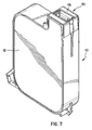
- Fig. 7 is a perspective view of the inkjet print cartridge of Fig. 1 with the TAB head assembly removed.
- Fig. 8 is a perspective view of the headland area of the inkjet print cartridge of Fig. 7.
- Fig. 9 is a top plan view of the headland area of the inkjet print cartridge of Fig. 7.
- Fig. 10 is a perspective view of a portion of the inkjet print cartridge of Fig. 3 illustrating the configuration of a seal which is formed between the ink cartridge body and the TAB head assembly.
- Fig. 11 is a top perspective view of a substrate structure containing heater resistors, ink channels, and vaporization chambers, which is mounted on the back of the TAB head assembly of Fig. 4.
- Fig. 12 is a top perspective view, partially cut away, of a portion of the TAB head assembly showing the relationship of an orifice with respect to a vaporization chamber, a heater resistor, and an edge of the substrate.
- Fig. 13 is a schematic cross-sectional view taken along line B-B of Fig. 10 showing the adhesive seal between the TAB head assembly and the print cartridge as well as the ink flow path around the edges of the substrate.
- Fig. 14 illustrates one process which may be used to form the preferred TAB head assembly.
- Fig. 15 shows the same substrate structure as that shown in Fig. 11 but having a different barrier layer pattern for improved printing performance.
- Fig. 16 is a top plan view of a magnified portion of the structure of Fig. 15.
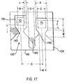
- Fig. 17 is a top plan view of a magnified portion of an alternative structure to the structure of Fig. 16.
- Fig. 18 is a top plan view of the structure of Fig. 15 expanded to show four resistors and the associated barrier structure.
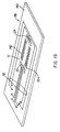
- Fig. 19 is a perspective view of the back surface of a flexible polymer circuit having ink orifices and cavities formed in it.
- Fig. 20 is a magnified perspective view, partially cut away, of a portion of the resulting TAB head assembly when the back surface of the flexible circuit in Fig. 19 is properly affixed to the barrier layer of the substrate structure shown in Fig. 15.
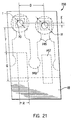
- Fig. 21 is a top plan view of the TAB head assembly portion shown in Fig. 19.
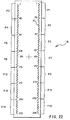
- Fig.22 is a view of one arrangement of orifices and the associated heater resistors on a printhead.
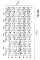
- Fig.23 is top plan view of one primitive of resistors and the associated ink vaporization chambers, ink channels and barrier architecture.
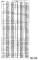
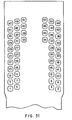
- Fig.24 is a table showing an embodiment of spatial location of 300 orifice nozzles.
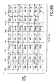
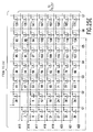
- Fig.25 is a schematic diagram of the heater resistors and the associated address lines, primitive select lines and ground lines which may be employed in the system.
- Fig.26 is an enlarged schematic diagram of the heater resistors and the associated address lines, primitive select lines and ground lines of the outlined portion of Fig.25.
- Fig.27 is a schematic diagram of one heater resistor of Figs. 25 and 26 and its associated address line, drive transistor, primitive select line and ground line.
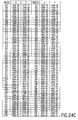
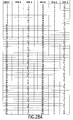
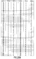
- Fig.28 is a table showing the primitive select line and address select line for each of the 300 heater orifice/resistor of one embodiment of system.
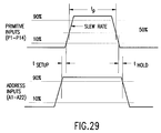
- Fig.29 is a schematic timing diagram for the setting of the address select and primitive select lines.
- Fig.30 is a schematic diagram of the firing sequence for the address select lines when the printer carriage is moving from left to right.
- Fig.31 is a diagram showing the layout of the contact pads on the TAB head assembly.
- an inkjet print cartridge 10 incorporating an embodiment of printhead is shown in simplified form for illustrative purposes.
- the inkjet print cartridge 10 includes an ink reservoir 12 and a printhead 14, where the printhead 14 is formed using Tape Automated Bonding (TAB).
- TAB head assembly 14 includes a nozzle member 16 comprising two parallel columns of offset holes or orifices 17 formed in a flexible polymer flexible circuit 18 by, for example, laser ablation.
- a back surface of the flexible circuit 18 includes conductive traces 36 formed thereon using a conventional photolithographic etching and/or plating process. These conductive traces 36 are terminated by large contact pads 20 designed to interconnect with a printer.
- the print cartridge 10 is designed to be installed in a printer so that the contact pads 20, on the front surface of the flexible circuit 18, contact printer electrodes providing externally generated energization signals to the printhead.
- Windows 22 and 24 extend through the flexible circuit 18 and are used to facilitate bonding of the other ends of the conductive traces 36 to electrodes on a silicon substrate containing heater resistors.
- the windows 22 and 24 are filled with an encapsulant to protect any underlying portion of the traces and substrate.
- the flexible circuit 18 is bent over the back edge of the print cartridge "snout" and extends approximately one half the length of the back wall 25 of the snout. This flap portion of the flexible circuit 18 is needed for the routing of conductive traces 36 which are connected to the substrate electrodes through the far end window 22.
- the contact pads 20 are located on the flexible circuit 18 which is secured to this wall and the conductive traces 36 are routed over the bend and are connected to the substrate electrodes through the windows 22, 24 in the flexible circuit 18.
- Fig. 2 shows a front view of the TAB head assembly 14 of Fig. 1 removed from the print cartridge 10 and prior to windows 22 and 24 in the TAB head assembly 14 being filled with an encapsulant.
- TAB head assembly 14 has affixed to the back of the flexible circuit 18 a silicon substrate 28 (not shown) containing a plurality of individually energizable thin film resistors. Each resistor is located generally behind a single orifice 17 and acts as an ohmic heater when selectively energized by one or more pulses applied sequentially or simultaneously to one or more of the contact pads 20.
- the orifices 17 and conductive traces 36 may be of any size, number, and pattern, and the various figures are designed to show simply and clearly the features of this embodiment. The relative dimensions of the various features have been greatly adjusted for the sake of clarity.
- the orifice 17 pattern on the flexible circuit 18 shown in Fig. 2 may be formed by a masking process in combination with a laser or other etching means in a step-and-repeat process, which would be readily understood by one of ordinary skilled in the art after reading this disclosure.
- Fig. 14, to be described in detail later, provides additional details of this process. Further details regarding TAB head assembly 14 and flexible circuit 18 are provided below.
- Fig. 3 is a perspective view of a simplified schematic of the inkjet print cartridge of Fig. 1for illustrative purposes.
- Fig. 4 is a perspective view of the front surface of the Tape Automated Bonding (TAB) printhead assembly (hereinafter "TAB head assembly”) removed from the simplified schematic print cartridge of Fig. 3.
- TAB Tape Automated Bonding
- Fig. 5 shows the back surface of the TAB head assembly 14 of Fig. 4 showing the silicon die or substrate 28 mounted to the back of the flexible circuit 18 and also showing one edge of the barrier layer 30 formed on the substrate 28 containing ink channels and vaporization chambers.
- Fig. 7 shows greater detail of this barrier layer 30 and will be discussed later. Shown along the edge of the barrier layer 30 are the entrances to the ink channels 32 which receive ink from the ink reservoir 12.
- the conductive traces 36 formed on the back of the flexible circuit 18 terminate in contact pads 20 ( shown in Fig. 4) on the opposite side of the flexible circuit 18.
- the windows 22 and 24 allow access to the ends of the conductive traces 36 and the substrate electrodes 40 (shown in Fig. 6) from the other side of the flexible circuit 18 to facilitate bonding.
- Fig. 6 shows a side view cross-section taken along line A-A in Fig. 5 illustrating the connection of the ends of the conductive traces 36 to the electrodes 40 formed on the substrate 28.
- a portion 42 of the barrier layer 30 is used to insulate the ends of the conductive traces 36 from the substrate 28.
- Fig. 7 shows the print cartridge 10 of Fig. 1 with the TAB head assembly 14 removed to reveal the headland pattern 50 used in providing a seal between the TAB head assembly 14 and the printhead body.
- Fig. 8 shows the headland area in enlarged perspective view.
- Fig. 9 shows the headland area in an enlarged top plan view. The headland characteristics are exaggerated for clarity. Shown in Figs. 8 and 9 is a central slot 52 in the print cartridge 10 for allowing ink from the ink reservoir 12 to flow to the back surface of the TAB head assembly 14.
- the headland pattern 50 formed on the print cartridge 10 is configured so that a bead of epoxy adhesive (not shown) dispensed on the inner raised walls 54 and across the wall openings 55 and 56 (so as to circumscribe the substrate when the TAB head assembly 14 is in place) will form an ink seal between the body of the print cartridge 10 and the back of the TAB head assembly 14 when the TAB head assembly 14 is pressed into place against the headland pattern 50.
- Other adhesives which may be used include hot-melt, silicone, UV curable adhesive, and mixtures thereof.
- a patterned adhesive film may be positioned on the headland, as opposed to dispensing a bead of adhesive.
- the TAB head assembly 14 of Fig. 5 When the TAB head assembly 14 of Fig. 5 is properly positioned and pressed down on the headland pattern 50 in Fig. 8 after the adhesive (not shown) is dispensed, the two short ends of the substrate 28 will be supported by the surface portions 57 and 58 within the wall openings 55 and 56. Additional details regarding adhesive 90 are shown in Fig. 13.
- the configuration of the headland pattern 50 is such that, when the substrate 28 is supported by the surface portions 57 and 58, the back surface of the flexible circuit 18 will be slightly above the top of the raised walls 54 and approximately flush with the flat top surface 59 of the print cartridge 10. As the TAB head assembly 14 is pressed down onto the headland 50, the adhesive is squished down.
- the adhesive From the top of the inner raised walls 54, the adhesive overspills into the gutter between the inner raised walls 54 and the outer raised wall 60 and overspills somewhat toward the slot 52. From the wall openings 55 and 56, the adhesive squishes inwardly in the direction of slot 52 and squishes outwardly toward the outer raised wall 60, which blocks further outward displacement of the adhesive.
- the outward displacement of the adhesive not only serves as an ink seal, but encapsulates the conductive traces in the vicinity of the headland 50 from underneath to protect the traces from ink.
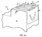
- Fig. 10 shows a portion of the completed print cartridge 10 of Fig. 3 illustrating, by cross-hatching, the location of the underlying adhesive 90 (not shown) which forms the seal between the TAB head assembly 14 and the body of the print cartridge 10.
- the adhesive is located generally between the dashed lines surrounding the array of orifices 17, where the outer dashed line 62 is slightly within the boundaries of the outer raised wall 60 in Fig. 7, and the inner dashed line 64 is slightly within the boundaries of the inner raised walls 54 in Fig. 7.
- the adhesive is also shown being squished through the wall openings 55 and 56 (Fig. 7) to encapsulate the traces leading to electrodes on the substrate. A cross-section of this seal taken along line B-B in Fig. 10 is also shown in Fig. 13, to be discussed later.
- This seal formed by the adhesive 90 circumscribing the substrate 28 allows ink to flow from slot 52 and around the sides of the substrate to the vaporization chambers formed in the barrier layer 30, but will prevent ink from seeping out from under the TAB head assembly 14.
- this adhesive seal 90 provides a strong mechanical coupling of the TAB head assembly 14 to the print cartridge 10, provides a fluidic seal, and provides trace encapsulation.
- the adhesive seal is also easier to cure than prior art seals, and it is much easier to detect leaks between the print cartridge body and the printhead, since the sealant line is readily observable. Further details on adhesive seal 90 are shown in Fig. 13.
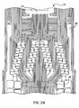
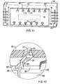
- Fig. 11 is a front perspective view of the silicon substrate 28 which is affixed to the back of the flexible circuit 18 in Fig. 5 to form the TAB head assembly 14. Silicon substrate 28 has formed on it, using conventional photolithographic techniques, two rows or colums of thin film resistors 70, shown in Fig. 11 exposed through the vaporization chambers 72 formed in the barrier layer 30.
- the substrate 28 is approximately one-half inch long and contains 300 heater resistors 70, thus enabling a resolution of 600 dots per inch.
- Heater resistors 70 may instead be any other type of ink ejection element, such as a piezoelectric pump-type element or any other conventional element.
- element 70 in all the various figures may be considered to be piezoelectric elements in an alternative embodiment without affecting the operation of the printhead.
- electrodes 74 are also formed on the substrate 28 for connection to the conductive traces 36 (shown by dashed lines) formed on the back of the flexible circuit 18.
- a demultiplexer 78 shown by a dashed outline in Fig. 11, is also formed on the substrate 28 for demultiplexing the incoming multiplexed signals applied to the electrodes 74 and distributing the signals to the various thin film resistors 70.
- the demultiplexer 78 enables the use of much fewer electrodes 74 than thin film resistors 70. Having fewer electrodes allows all connections to the substrate to be made from the short end portions of the substrate, as shown in Fig. 4, so that these connections will not interfere with the ink flow around the long sides of the substrate.
- the demultiplexer 78 may be any decoder for decoding encoded signals applied to the electrodes 74.
- the demultiplexer has input leads (not shown for simplicity) connected to the electrodes 74 and has output leads (not shown) connected to the various resistors 70.
- the demultiplexer 78 circuity is discussed in further detail below.
- barrier layer 30 which may be a layer of photoresist or some other polymer, in which is formed the vaporization chambers 72 and ink channels 80.
- a portion 42 of the barrier layer 30 insulates the conductive traces 36 from the underlying substrate 28, as previously discussed with respect to Fig. 4.
- a thin adhesive layer 84 (not shown), such as an uncured layer of poly-isoprene photoresist, is applied to the top surface of the barrier layer 30.
- a separate adhesive layer may not be necessary if the top of the barrier layer 30 can be otherwise made adhesive.
- the resulting substrate structure is then positioned with respect to the back surface of the flexible circuit 18 so as to align the resistors 70 with the orifices formed in the flexible circuit 18.
- This alignment step also inherently aligns the electrodes 74 with the ends of the conductive traces 36.
- the traces 36 are then bonded to the electrodes 74. This alignment and bonding process is described in more detail later with respect to Fig. 14.
- the aligned and bonded substrate/flexible circuit structure is then heated while applying pressure to cure the adhesive layer 84 and firmly affix the substrate structure to the back surface of the flexible circuit 18.
- Fig. 12 is an enlarged view of a single vaporization chamber 72, thin film resistor 70, and frustum shaped orifice 17 after the substrate structure of Fig. 11 is secured to the back of the flexible circuit 18 via the thin adhesive layer 84.
- a side edge of the substrate 28 is shown as edge 86.
- ink flows from the ink reservoir 12 around the side edge 86 of the substrate 28, and into the ink channel 80 and associated vaporization chamber 72, as shown by the arrow 88.
- a thin layer of the adjacent ink is superheated, causing explosive vaporization and, consequently, causing a droplet of ink to be ejected through the orifice 17.
- the vaporization chamber 72 is then refilled by capillary action.
- the barrier layer 30 is approximately 25 ⁇ m (1 mil) thick, the substrate 28 is approximately 500 ⁇ m (20 mils) thick, and the flexible circuit 18 is approximately 50 ⁇ m (2 mils) thick.
- Fig. 13 Shown in Fig. 13 is a side elevational view cross-section taken along line B-B in Fig. 10 showing a portion of the adhesive seal 90, applied to the inner raised wall 54 and wall openings 55, 56, surrounding the substrate 28 and showing the substrate 28 being adhesively secured to a central portion of the flexible circuit 18 by the thin adhesive layer 84 on the top surface of the barrier layer 30 containing the ink channels and vaporization chambers 92 and 94.
- Fig. 13 also illustrates how ink 88 from the ink reservoir 12 flows through the central slot 52 formed in the print cartridge 10 and flows around the edges 86 of the substrate 28 through ink channels 80 into the vaporization chambers 92 and 94.
- Thin film resistors 96 and 98 are shown within the vaporization chambers 92 and 94, respectively. When the resistors 96 and 98 are energized, the ink within the vaporization chambers 92 and 94 is ejected, as illustrated by the emitted drops of ink 101 and 102.
- the edge feed feature where ink flows around the edges 86 of the substrate 28 and directly into ink channels 80, has a number of advantages over previous center feed printhead designs which form an elongated central hole or slot running lengthwise in the substrate to allow ink to flow into a central manifold and ultimately to the entrances of ink channels.
- One advantage is that the substrate or die 28 width can be made narrower, due to the absence of the elongated central hole or slot in the substrate . Not only can the substrate be made narrower, but the length of the edge feed substrate can be shorter, for the same number of nozzles, than the center feed substrate due to the substrate structure now being less prone to cracking or breaking without the central ink feed hole.
- This shortening of the substrate 28 enables a shorter headland 50 in Fig. 8 and, hence, a shorter print cartridge snout.
- the star wheels can be located closer to the pinch rollers to ensure better paper/roller contact along the transport path of the print cartridge snout.
- by making the substrate smaller more substrates can be formed per wafer, thus lowering the material cost per substrate.
- edge feed feature manufacturing time is saved by not having to etch a slot in the substrate, and the substrate is less prone to breakage during handling. Further, the substrate is able to dissipate more heat, since the ink flowing across the back of the substrate and around the edges of the substrate acts to draw heat away from the back of the substrate.
- the edge feed design Be eliminating the manifold as well as the slot in the substrate, the ink is able to flow more rapidly into the vaporization chambers, since there is less restriction on the ink flow. This more rapid ink flow improves the frequency response of the printhead, allowing higher printing rates from a given number of orifices. Further, the more rapid ink flow reduces crosstalk between nearby vaporization chambers caused by variations in ink flow as the heater elements in the vaporization chambers are fired.
- the ink reservoir contains two separate ink sources, each containing a different color of ink.
- the central slot 52 in Fig. 13 is bisected, as shown by the dashed line 103, so that each side of the central slot 52 communicates with a separate ink source. Therefore, the left linear array of vaporization chambers can be made to eject one color of ink, while the right linear array of vaporization chambers can be made to eject a different color of ink.
- This concept can even be used to create a four color printhead, where a different ink reservoir feeds ink to ink channels along each of the four sides of the substrate.
- a four-edge design would be used, preferably using a square substrate for symmetry.
- Fig. 14 illustrates one method for forming the preferred embodiment of the TAB head assembly 14.
- the starting material is a Kapton or Upilex type polymer tape 104, although the tape 104 can be any suitable polymer film which is acceptable for use in the below-described procedure. Some such films may comprise teflon, polyamide, polymethylmethacrylate, polycarbonate, polyester, polyamide polyethylene-terephthalate or mixtures thereof.
- the tape 104 is typically provided in long strips on a reel 105.
- Sprocket holes 106 along the sides of the tape 104 are used to accurately and securely transport the tape 104.
- the sprocket holes 106 may be omitted and the tape may be transported with other types of fixtures.
- the tape 104 is already provided with conductive copper traces 36, such as shown in Figs. 2, 4 and 5, formed thereon using conventional metal deposition and photolithographic processes.
- conductive copper traces 36 such as shown in Figs. 2, 4 and 5, formed thereon using conventional metal deposition and photolithographic processes.
- the particular pattern of conductive traces depends on the manner in which it is desired to distribute electrical signals to the electrodes formed on silicon dies, which are subsequently mounted on the tape 104.
- the tape 104 is transported to a laser processing chamber and laser-ablated in a pattern defined by one or more masks 108 using laser radiation 110, such as that generated by an Excimer laser 112 of the F2, ArF, KrCl, KrF, or Xecl type.
- laser radiation 110 such as that generated by an Excimer laser 112 of the F2, ArF, KrCl, KrF, or Xecl type.
- the masked laser radiation is designated by arrows 114.
- such masks 108 define all of the ablated features for an extended area of the tape 104, for example encompassing multiple orifices in the case of an orifice pattern mask 108, and multiple vaporization chambers in the case of a vaporization chamber pattern mask 108.
- patterns such as the orifice pattern, the vaporization chamber pattern, or other patterns may be placed side by side on a common mask substrate which is substantially larger than the laser beam. Then such patterns may be moved sequentially into the beam.
- the masking material used in such masks will preferably be highly reflecting at the laser wavelength, consisting of, for example, a multilayer dielectric or a metal such as aluminum.
- the orifice pattern defined by the one or more masks 108 may be that generally shown in Fig. 21. Multiple masks 108 may be used to form a stepped orifice taper as shown in Fig. 12.
- a separate mask 108 defines the pattern of windows 22 and 24 shown in Figs. 1 and 2; however, in the preferred embodiment, the windows 22 and 24 are formed using conventional photolithographic methods prior to the tape 104 being subjected to the processes shown in Fig. 14.
- one or more masks 108 would be used to form the orifices and another mask 108 and laser energy level (and/or number of laser shots) would be used to define the vaporization chambers, ink channels, and manifolds which are formed through a portion of the thickness of the tape 104.
- the laser system for this process generally includes beam delivery optics, alignment optics, a high precision and high speed mask shuttle system, and a processing chamber including a mechanism for handling and positioning the tape 104.
- the laser system uses a projection mask configuration wherein a precision lens 115 interposed between the mask 108 and the tape 104 projects the Excimer laser light onto the tape 104 in the image of the pattern defined on the mask 108.
- the masked laser radiation exiting from lens 115 is represented by arrows 116.
- Such a projection mask configuration is advantageous for high precision orifice dimensions, because the mask is physically remote from the nozzle member. Soot is naturally formed and ejected in the ablation process, traveling distances of about one centimeter from the nozzle member being ablated. If the mask were in contact with the nozzle member, or in proximity to it, soot buildup on the mask would tend to distort ablated features and reduce their dimensional accuracy. In the preferred embodiment, the projection lens is more than two centimeters from the nozzle member being ablated, thereby avoiding the buildup of any soot on it or on the mask.
- Ablation is well known to produce features with tapered walls, tapered so that the diameter of an orifice is larger at the surface onto which the laser is incident, and smaller at the exit surface.
- the taper angle varies significantly with variations in the optical energy density incident on the nozzle member for energy densities less than about two joules per square centimeter. If the energy density were uncontrolled, the orifices produced would vary significantly in taper angle, resulting in substantial variations in exit orifice diameter. Such variations would produce deleterious variations in ejected ink drop volume and velocity, reducing print quality.
- the optical energy of the ablating laser beam is precisely monitored and controlled to achieve a consistent taper angle, and thereby a reproducible exit diameter.
- a taper is beneficial to the operation of the orifices, since the taper acts to increase the discharge speed and provide a more focused ejection of ink, as well as provide other advantages.
- the taper may be in the range of 5 to 15 degrees relative to the axis of the orifice.
- the polymer tape 104 is stepped, and the process is repeated. This is referred to as a step-and-repeat process.
- the total processing time required for forming a single pattern on the tape 104 may be on the order of a few seconds.
- a single mask pattern may encompass an extended group of ablated features to reduce the processing time per nozzle member.
- Laser ablation processes have distinct advantages over other forms of laser drilling for the formation of precision orifices, vaporization chambers, and ink channels.
- short pulses of intense ultraviolet light are absorbed in a thin surface layer of material within about 1 micrometer or less of the surface.
- Preferred pulse energies are greater than about 100 millijoules per square centimeter and pulse durations are shorter than about 1 microsecond.
- the intense ultraviolet light photodissociates the chemical bonds in the material.
- the absorbed ultraviolet energy is concentrated in such a small volume of material that it rapidly heats the dissociated fragments and ejects them away from the surface of the material. Because these processes occur so quickly, there is no time for heat to propagate to the surrounding material.
- laser ablation can also form chambers with substantially flat bottom surfaces which form a plane recessed into the layer, provided the optical energy density is constant across the region being ablated. The depth of such chambers is determined by the number of laser shots, and the power density of each.
- Laser-ablation processes also have numerous advantages as compared to conventional lithographic electroforming processes for forming nozzle members for inkjet printheads. For example, laser-ablation processes generally are less expensive and simpler than conventional lithographic electroforming processes.
- polymer nozzle members can be fabricated in substantially larger sizes (i.e., having greater surface areas) and with nozzle geometries that are not practical with conventional electroforming processes.
- unique nozzle shapes can be produced by controlling exposure intensity or making multiple exposures with a laser beam being reoriented between each exposure. Examples of a variety of nozzle shapes are described in copending application Serial No.
- nozzle members by laser-ablating a polymer material
- L nozzle length
- D nozzle diameter
- LID ratio exceeds unity.
- One advantage of extending a nozzle's length relative to its diameter is that orifice-resistor positioning in a vaporization chamber becomes less critical.
- laser-ablated polymer nozzle members for inkjet printers have characteristics that are superior to conventional electroformed orifice plates.
- laser-ablated polymer nozzle members are highly resistant to corrosion by water-based printing inks and are generally hydrophobic.
- laser-ablated polymer nozzle members have a relatively low elastic modulus, so built-in stress between the nozzle member and an underlying substrate or barrier layer has less of a tendency to cause nozzle member-to-barrier layer delamination.
- laser-ablated polymer nozzle members can be readily fixed to, or formed with, a polymer substrate.
- the wavelength of such an ultraviolet light source will lie in the 150 nm to 400 nm range to allow high absorption in the tape to be ablated.
- the energy density should be greater than about 100 millijoules per square centimeter with a pulse length shorter than about 1 microsecond to achieve rapid ejection of ablated material with essentially no heating of the surrounding remaining material.
- a next step in the process is a cleaning step wherein the laser ablated portion of the tape 104 is positioned under a cleaning station 117. At the cleaning station 117, debris from the laser ablation is removed according to standard industry practice.
- the tape 104 is then stepped to the next station, which is an optical alignment station 118 incorporated in a conventional automatic TAB bonder, such as an inner lead bonder commercially available from Shinkawa Corporation, model number IL-20.
- the bonder is preprogrammed with an alignment (target) pattern on the nozzle member, created in the same manner and/or step as used to created the orifices, and a target pattern on the substrate, created in the same manner and/or step used to create the resistors.
- the nozzle member material is semi-transparent so that the target pattern on the substrate may be viewed through the nozzle member.
- the bonder then automatically positions the silicon dies 120 with respect to the nozzle members so as to align the two target patterns.
- the alignment of the silicon dies 120 with respect to the tape 104 is performed automatically using only commercially available equipment.
- By integrating the conductive traces with the nozzle member, such an alignment feature is possible.
- Such integration not only reduces the assembly cost of the printhead but reduces the printhead material cost as well.
- the automatic TAB bonder then uses a gang bonding method to press the ends of the conductive traces down onto the associated substrate electrodes through the windows formed in the tape 104.
- the bonder then applies heat, such as by using thermocompression bonding, to weld the ends of the traces to the associated electrodes.
- a schematic side view of one embodiment of the resulting structure is shown in Fig. 6.
- Other types of bonding can also be used, such as ultrasonic bonding, conductive epoxy, solder paste, or other well-known means.
- the tape 104 is then stepped to a heat and pressure station 122.
- an adhesive layer 84 exists on the top surface of the barrier layer 30 formed on the silicon substrate.
- the silicon dies 120 are then pressed down against the tape 104, and heat is applied to cure the adhesive layer 84 and physically bond the dies 120 to the tape 104.
- the tape 104 steps and is optionally taken up on the take-up reel 124.
- the tape 104 may then later be cut to separate the individual TAB head assemblies from one another.
- the resulting TAB head assembly is then positioned on the print cartridge 10, and the previously described adhesive seal 90 is formed to firmly secure the nozzle member to the print cartridge, provide an ink-proof seal around the substrate between the nozzle member and the ink reservoir, and encapsulate the traces in the vicinity of the headland so as to isolate the traces from the ink.
- Peripheral points on the flexible TAB head assembly are then secured to the plastic print cartridge 10 by a conventional melt-through type bonding process to cause the polymer flexible circuit 18 to remain relatively flush with the surface of the print cartridge 10, as shown in Fig. 1.
- the printhead nozzles must be placed closer together. This requires that both heater resistors and the associated orifices be placed closer together.
- the firing frequency of the resistors must be increased.
- conventional ink channel barrier designs either do not allow the vaporization chambers to adequately refill or allow extreme blowback or catastrophic overshoot and puddling on the exterior of the nozzle member.
- the closer spacing of the resistors created space problems and restricted possible barrier solutions due to manufacturing concerns.
- the TAB head assembly architecture shown schematically in Fig. 15 is advantageous when a very high density of dots is required to be printed (e.g., 600 dpi) .
- a very high density of dots e.g., 600 dpi
- firing rates e.g., 12 kHz
- cross-talk between neighboring vaporization chambers becomes a serious problem.
- bubble growth initiated by a resistor displaces ink outward in the form of a drop.
- ink is also displaced back into the ink channel.
- blowback volume The quantity of ink so displaced is often described as "blowback volume.”
- the ratio of ejected volume to blowback volume is an indication of ejection efficiency, which may be on the order of about 1:1 for the TAB head assembly 14 of Fig. 11.
- blowback volume causes displacements in the menisci of neighboring nozzles. When these neighboring nozzles are fired, such displacements of their menisci cause deviations in drop volume from the nominally equilibrated situation resulting in nonuniform dots being printed.
- FIG. 9 A second embodiment shown in the TAB head assembly architecture of Fig.15 is designated to minimize such cross-talk effects.
- Elements in Figs. 9 and 13 which are labelled with the same numbers are similar in structure and operation. The significant differences between the structures of Figs. 9 and 13 include the barrier layer pattern and the increased density of the vaporization chambers.
- vaporization chambers 130 and ink channels 132 are shown formed in barrier layer 134.
- Ink channels 132 provide an ink path between the source of ink and the vaporization chambers 130.
- the flow of ink into the ink channels 132 and into the vaporization chambers 130 is generally similar to that described with respect to Figs. 10 and 11, whereby ink flows around the long side edges 86 of the substrate 28 and into the ink channels 132.
- the vaporization chambers 130 and ink channels 132 may be formed in the barrier layer 134 using conventional photolithographic techniques.
- the barrier layer 134 may be similar to the barrier layer 30 in Figs. 5 and 10 and may comprise any high quality photoresist, such as Vacrel or Parad .
- Thin film resistors 70 in Fig. 15 are similar to those described with respect to Fig. 11 and are formed on the surface of the silicon substrate 28.
- resistors 70 may instead be well known piezoelectric pump-type ink ejection elements or any other conventional ink ejection elements where vaporization of ink is not necessarily occurring in chambers 130. If a piezoelectric ink ejection element is used, such chambers 130 may be broadly referred to as ink ejection chambers.
- the substrate structure of Fig. 15 is affixed to the nozzle member 136 of Fig. 17 in the manner shown in Fig. 19 which is described in greater detail later.
- the resulting TAB head assembly is very similar to the TAB head assembly 14 in Figs. 2, 4, 5, and 6.
- the particular architecture of the ink channels 132 in Fig. 15 provides advantages over the architecture shown in Fig. 11. Further details and other advantages of the TAB head assembly architecture will be described with respect to Fig. 16, which is a magnified top plan view of the portion of Fig. 15 shown within dashed outline 150.
- the architecture of the ink channels 132 in Fig. 16 has the following differences from the architecture shown in Fig. 11.
- the relatively narrow constriction points or pinch point gaps 145 created by the pinch points 146 in the ink channels 132 provide viscous damping during refill of the vaporization chambers 130 after firing. This viscous damping helps minimize cross-talk between neighboring vaporization chambers 130.
- the pinch points 146 also help control ink blow-back and bubble collapse after firing to improve the uniformity of ink drop ejection.
- the addition of "peninsulas" 149 extending from the barrier body out to the edge of the substrate provided fluidic isolation of the vaporization chambers 130 from each other to prevent cross-talk and allowed support of the nozzle member 136 at the edge of the substrate.
- the enlarged areas or reefs 148 formed on the ends of the peninsulas 149 near the entrance to each ink channel 132 increase the nozzle member 136 support area at the edges of the barrier layer 134 so that the nozzle member 136 lies relatively flat on barrier layer 134 when affixed to barrier layer 134.
- Adjacent reefs 148 also act to constrict the entrance of the ink channels 132 so as to help filter large foreign particles.
- the pitch D of the vaporization chambers 130 shown in Fig. 16 provides for 600 dots per inch (dpi) printing using two rows of vaporization chambers 130 as shown in Fig. 22 and to be described below.
- a small offset E (shown in Fig. 21) is provided between vaporization chambers 130.
- This small offset E allows adjacent resistors 70 to be fired at slightly different times when the TAB head assembly is scanning across the recording medium to further minimize cross-talk effects between adjacent vaporization chambers 130.
- the definition of the dimensions of the various elements shown in Figs. 16, 17, 20 and 21 are provided in Table I.
- Fig. 17 is a modified top plan view of the portion of the ink channels 132 shown in Fig. 16.
- the architecture of the ink channels 132 in Fig. 17 has the following differences from the architecture shown in Fig. 16. As the shelf length U decreases in length, the nozzle frequency increases. In the embodiment shown in FIG. 17 the shelf length is reduced.
- Edge feed permits use of a second saw cut partially through the wafer to allowing a shorter shelf length, U, to be formed. Alternatively, precise etching may be used. This shelf length is shorter than that of other commercially available printer cartridges and permits firing at much higher frequencies.
- the frequency limit of a thermal inkjet pen is limited by resistance in the flow of ink to the nozzle. However, some resistance in ink flow is necessary to damp meniscus oscillation, but too much resistance limits the upper frequency at which a print cartridge can operate.
- Ink flow resistance is intentionally controlled by the pinch point gap 145 gap adjacent the resistor with a well-defined length and width. The distance of the resistor 70 from the substrate edge varies with the firing patterns of the TAB head assembly.
- An additional component to the fluid impedance is the entrance to the firing chamber.
- the entrance comprises a thin region between the nozzle member 16 and the substrate 28 and its height is essentially a function of the thickness of the barrier layer 134. This region has high fluid impedance, since its height is small.
- the refill ink channel was reduced to a minimum shelf length, to allow the fastest possible refill, and "pinched" to the minimum width, to create the best damping.
- the short shelf length reduced the mass of the moving ink during ink chamber refill, thus reducing the sensitivity to damping features. This allowed wider processing tolerances while at the same time maintaining controlled damping.
- the principal difference is that the peninsulas 149 have been shortened and the reefs 148 have been removed. In addition, every other peninsula 149 has been shortened further to the pinch points 146. Also as shown in Fig. 17 the shape of the pinch points 146 have been modified.
- the pinch points 146 can be on one or both sides of the ink channel 130 with various tip configurations.
- Fig. 16 shows the various elements formed in the barrier layer 134 shown in Fig. 16 in Table III below.
- Fig. 18 shows the effect of the offset from resistor to resistor on the shape long and shortened peninsulas due to the pinch points 146.
- Fig. 19 is a preferred nozzle member 136 in the form of a flexible polymer tape 140, which, when affixed to the substrate structure shown in Fig. 15, forms a TAB head assembly similar to that shown in Figs. 4 and 5. Elements in Figs. 5 and 15 which are labelled with the same numbers are similar in structure and operation.
- the flexible polymer nozzle member 136 in Fig. 19 primarily differs from the flexible circuit 18 in Fig. 5 by the increased density of laser-ablated nozzles 17 in the nozzle member 136 (to produce a higher printing resolution) and by the inclusion of cavities 142 which are laser-ablated through a partial thickness of the nozzle member 136.
- a separate mask 108 in the process shown in Fig. 14 may be used to define the pattern of cavities 142 in the nozzle member 136.
- a second laser source may be used to output the proper energy and pulse length to laser ablate cavities 142 through only a partial thickness of the nozzle member 136.
- Conductors 36 on flexible circuit 140 provide an electrical path between the contact pads 20 (Fig. 4) and the electrodes 74 on the substrate 28 (Fig. 15). Conductors 36 are formed directly on flexible circuit 140 as previously described with respect to Fig. 5.
- Fig. 20 is a magnified, partially cut away view in perspective of the portion of the nozzle member 136 shown in the dashed outline 154 of Fig. 19 after the nozzle member 136 has been properly positioned over the substrate structure of Fig. 20 to form a TAB head assembly 158 similar to the TAB head assembly 14 in Fig. 5.
- the nozzles 17 are aligned over the vaporization chambers 130, and the cavities 142 are aligned over the ink channels 132.
- Fig. 20 also illustrates the ink flow 160 from an ink reservoir generally situated behind the substrate 28 as the ink flows over an edge 86 of the substrate 28 and enters cavities 142 and ink channels 132.
- Preferred dimensions A, B, and C in Fig. 20 are provided in Table IV below, where dimension C is the thickness of the nozzle member 136, dimension B is the thickness of the barrier layer 134, and dimension A is the thickness of the substrate 28.
- Fig. 21 is a top plan view of the portion of the TAB head assembly 158 shown in Fig. 20, where the vaporization chambers 130 and ink channels 132 can be seen through the nozzle member 136.
- the various dimensions of the cavities 142, the nozzles 17, and the separations between the various elements are identified in Table IV below.
- dimension H is the entrance diameter of the nozzles 17, while dimension I is the exit diameter of the nozzles 17. The other dimensions are self-explanatory.
- the cavities 142 minimize the viscous damping of ink during refill as the ink flows into the ink channels 132. This helps compensate for the increased viscous damping provided by the pinch points 146, reefs 148, and increased length of the ink channels 132 along the substrate shelf. Minimizing viscous damping helps increase the maximum firing rate of the resistors 70, since ink can enter into the ink channels 132 more quickly after firing.
- the damping function is provided primarily by the pinch points rather than the viscous damping which is different individual vaporization chambers due to the different shelf lengths for individual vaporization chambers caused by the offsets, E, between the vaporization chambers.
- Tables I, II and III above lists the nominal values of the various dimensions A-U of the TAB head assembly structure of Figs. 13-18 as well as their preferred ranges. It should be understood that the preferred ranges and nominal values of an actual embodiment will depend upon the intended operating environment of the TAB head assembly, including the type of ink used, the operating temperature, the printing speed, and the dot density.
- the orifices 17 in the nozzle member 16 of the TAB head assembly are generally arranged in two major columns of orifices 17 as shown in Fig. 22.
- the orifices 17 are conventionally assigned a number as shown, starting at the top right as the TAB head assembly as viewed from the external surface of the nozzle member 16 and ending in the lower left, thereby resulting in the odd numbers being arranged in one column and even numbers being arranged in the second column.
- other numbering conventions may be followed, but the description of the firing order of the orifices 17 associated with this numbering system has advantages.
- the orifices/resistors in each column are spaced 1/300 of an inch apart in the long direction of the nozzle member.
- the orifices and resistors in one column are offset from the orifice/resistors in the other column in the long direction of the nozzle member by 1/600 of an inch, thus, providing 600 dots per inch (dpi) printing.
- the orifices 17, while aligned in two major columns as described, are further arranged in an offset pattern within each column to match the offset heater resistors 70 disposed in the substrate 28 as illustrated in Figs. 22 and 23.
- a small offset E (shown in Fig. 21) is provided between resistors.
- This small offset E allows adjacent resistors 70 to be fired at slightly different times when the TAB head assembly is scanning across the recording medium to further minimize cross-talk effects between adjacent vaporization chambers 130.
- the resistors are fired at twent two different times, the offset allows the ejected ink drops from different nozzles to be placed in the same horizontal position on the print media. .
- the resistors 70 are coupled to electrical drive circuitry (not shown in Fig. 22) and are organized in groups of fourteen primitives which consist of four primitives of twenty resistors (P1, P2, P13 and P14) and ten primitives of twenty two resistors for a total of 300 resistors.
- the fourteen resistor primitives (and associated orifices) are shown in Fig. 22.
- Fig. 23 shows the offset of the resistors and the ink channels 132, peninsulas 149, pinch point gaps 145 and pinch points 146 of primitive P5.
- the spatial location of the 300 resistor/orifices with respect to the centroid of the substrate is provided in Fig. 24.
- the TAB head assembly orifices 17 are positioned directly over the heater resistors 70 and are positioned relative to its most adjacent neighbor in accordance with Fig. 16. This placement and firing sequence provides a more uniform frequency response for all resistors 70 and reduces the crosstalk between adjacent vaporization chambers.
- the firing heater resistors 70 of the preferred embodiment are organized as fourteen primitive groups of twenty or twenty-two resistors.
- each resistor (numbered 1 through 300 and corresponding to the orifices 17 of Fig. 22) is controlled by its own FET drive transistor, which shares its control input Address Select (A1-A22) with thirteen other resistors.
- Each resistor is tied to nineteen or twenty-one other resistors by a common node Primitive Select (PS1-PS14).
- Fig. 27 is a schematic diagram of an individual heater resistor and its FET drive transistor. As shown in Fig. 27, Address Select and Primitive Select lines also contain transistors for draining unwanted electrostatic discharge and pull down resistors to place all unselected addresses in an off state. Table V and Fig.
- the Address Select lines are sequentially turned on via TAB head assembly interface circuitry according to a firing order counter located in the printer and sequenced (independently of the data directing which resistor is to be energized) from A1 to A22 when printing form left to right and from A22 to A1 when printing from right to left.
- the print data retrieved from the printer memory turns on any combination of the Primitive Select lines.
- Primitive Select lines (instead of Address Select lines) are used in the preferred embodiment to control the pulse width. Disabling Address Select lines while the drive transistors are conducting high current can cause avalanche breakdown and consequent physical damage to MOS transistors. Accordingly, the Address Select lines are "set" before power is applied to the Primitive Select lines, and conversely, power is turned off before the Address Select lines are changed as shown in Fig. 29.
- each primitive is selectively fired by powering the associated primitive select interconnection.
- To provide uniform energy per heater resistor only one resistor is energized at a time per primitive.
- any number of the primitive selects may be enabled concurrently.
- Each enabled primitive select thus delivers both power and one of the enable signals to the driver transistor.
- the other enable signal is an address signal provided by each address select line only one of which is active at a time.
- Each address select line is tied to all of the switching transistors so that all such switching devices are conductive when the interconnection is enabled. Where a primitive select interconnection and an address select line for a heater resistor are both active simultaneously, that particular heater resistor is energized.
- firing a particular resistor requires applying a control voltage at its "Address Select" terminal and an electrical power source at its "Primitive Select” terminal. Only one Address Select line is enabled at one time. This ensures that the Primitive Select and Group Return lines supply current to at most one resistor at a time. Otherwise, the energy delivered to a heater resistor would be a function of the number of resistors 70 being fired at the same time.
- Fig. 30 shows the firing sequence when the print carriage is scanning from left to right. The firing sequence is reversed when scanning from right to left. A brief rest period of approximately ten percent of the period is allowed between cycles. This rest period prevents Address Select cycles from overlapping due to printer carriage velocity variations.
- the interconnections for controlling the TAB head assembly driver circuitry include separate primitive select and primitive common interconnections.
- the driver circuity of the preferred embodiment comprises an array of fourteen primitives, fourteen primitive commons, and twenty-two address select lines, thus requiring 50 interconnections to control 300 firing resistors.
- the integration of both heater resistors and FET driver transistors onto a common substrate creates the need for additional layers of conductive circuitry on the substrate so that the transistors could be electrically connected to the resistors and other components of the system. This creates a concentration of heat generation within the substrate.
- the print cartridge 10 is designed to be installed in a printer so that the contact pads 20, on the front surface of the flexible circuit 18, contact printer electrodes which couple externally generated energization signals to the TAB head assembly.
- To access the traces 36 on the back surface of the flexible circuit 18 from the front surface of the flexible circuit holes (vias) are formed through the front surface of the flexible circuit to expose the ends of the traces.
- the exposed ends of the traces are then plated with, for example, gold to form the contact pads 20 shown on the front surface of the flexible circuit in Fig. 2.
- the contact or interface pads 20 are assigned the functions listed in Table VI.
- Fig. 31 shows the location of the interface pads 20 on the TAB head assembly of Fig. 2.
Abstract
Description
- The present invention generally relates to an inkjet printing system.
- Thermal inkjet print cartridges operate by rapidly heating a small volume of ink to cause the ink to vaporize and be ejected through one of a plurality of orifices so as to print a dot of ink on a recording medium, such as a sheet of paper. Typically, the orifices are arranged in one or more linear arrays in a nozzle member. The properly sequenced ejection of ink from each orifice causes characters or other images to be printed upon the paper as the printhead is moved relative to the paper. The paper is typically shifted each time the printhead has moved across the paper. The thermal inkjet printer is fast and quiet, as only the ink strikes the paper. These printers produce high quality printing and can be made both compact and affordable.
- An inkjet printhead generally includes: (1) ink channels to supply ink from an ink reservoir to each vaporization chamber proximate to an orifice; (2) a metal orifice plate or nozzle member in which the orifices are formed in the required pattern; and (3) a silicon substrate containing a series of thin film resistors, one resistor per vaporization chamber.
- To print a single dot of ink, an electrical current from an external power supply is passed through a selected thin film resistor. The resistor is then heated, in turn superheating a thin layer of the adjacent ink within a vaporization chamber, causing explosive vaporization, and, consequently, causing a droplet of ink to be ejected through an associated orifice onto the paper.
- In an inkjet printhead, described in US-A-4,683,481, ink is fed from an ink reservoir to the various vaporization chambers through an elongated hole formed in the substrate. The ink then flows to a manifold area, formed in a barrier layer between the substrate and a nozzle member, then into a plurality of ink channels, and finally into the various vaporization chambers. This design may be classified as a "center" feed design, whereby ink is fed to the vaporization chambers from a central location then distributed outward into the vaporization chambers. Some disadvantages of this type of ink feed design are that manufacturing time is required to make the hole in the substrate, and the required substrate area is increased by at least the area of the hole. Also, once the hole is formed, the substrate is relatively fragile, making handling more difficult. Further, the manifold inherently provides some restriction of ink flow to the vaporization chambers such that the energization of heater elements within a vaporization chamber may affect the flow of ink into a nearby vaporization chamber, thus producing crosstalk which affects the amount of ink emitted by an orifice upon energization of a nearby heater element. More importantly, prior printhead design limited the ability of printheads to have the high nozzle densities and the high operating frequencies and firing rates required for increased resolution and throughput. Print resolution depends on the density of ink-ejecting orifices and heating resistors formed on the cartridge printhead substrate. Modern circuit fabrication techniques allow the placement of substantial numbers of resistors on a single printhead substrate. However, the number of resistors applied to the substrate is limited by the conductive components used to electrically connect the cartridge to external driver circuitry in the printer unit. Specifically, an increasingly large number of resistors requires a correspondingly large number of interconnection pads, leads, and the like. This increase in components and interconnects causes greater manufacturing/production costs, and increases the probability that defects will occur during the manufacturing process. In order to solve this problem, thermal inkjet printheads have been developed which incorporate pulse driver circuitry directly on the printhead substrate with the resistors. The incorporation of driver circuitry on the printhead substrate in this manner reduces the number of interconnect components needed to electrically connect the cartridge to the printer unit.
- This results in an improved degree of production and operating efficiency. This development is described in U.S. Patent Nos. 4,719,477 and 5,122,812.
- To produce high-efficiency, integrated printing systems as described above, significant research has been conducted in order to develop improved transistor structures and methods for integrating the same into thermal inkjet printing units. The integration of driver components and printing resistors onto a common substrate results in a need for specialized, multi-layer connective circuitry so that the driver transistors can communicate with the resistors and other portions of the printing system. Typically, this connective circuitry involves a plurality of separate conductive layers, each being formed using conventional circuit fabrication techniques.
- To create the resistors, an electrically conducting layer is positioned on selected portions of the layer of resistive material in order to form covered sections of the resistive materials and uncovered sections thereof. The uncovered sections ultimately function as heating resistors in the printhead. The covered sections are used to form continuous conductive links between the electrical contact regions of the transistors and other components in the printing system. Thus, the layer of resistive material performs dual functions: as heating resistors in the system, and as direct conductive pathways to the drive transistors. This substantially eliminates the need to use multiple layers for carrying out these functions alone.
- A selected portion of protective material is then applied to the covered and uncovered sections of resistive material. Thereafter, an orifice plate having a plurality of openings through the plate was positioned on the protective material. Beneath the openings, a section of the protective material which was removed forms ink firing cavities or vaporization chambers. Positioned at the bottom surface of each chamber is one of the heater resistors. The electrical activation of each resistor causes the resistor to rapidly heat and vaporize a portion of the ink in the cavity. The rapidly formed (nucleated) ink bubble ejects a droplet of ink from the orifice associated with the activated resistor and ink firing vaporization chamber.
- To increase resolution and print quality, the printhead nozzles must be placed closer together. This requires that both heater resistors and the associated orifices be placed closer together. To increase printer throughput, the width of the printing swath must be increased by placing more nozzles on the print head. However, adding resistors and nozzles requires adding associated power and control interconnections. These interconnections are conventionally flexible wires or equivalent conductors that electrically connect the transistor drivers on the printhead to printhead interface circuitry in the printer. They may be contained in a ribbon cable that connects on one end to control circuitry within the printer and on the other end to driver circuitry on the printhead. An increased number of heater resistors spaced closer together also creates a greater likelihood of crosstalk and increased difficulty in supplying ink to each vaporization chamber quickly.
- Interconnections are a major source of cost in printer design, and adding them in increase the number of heater resistors increases the cost and reduces the reliability of the printer. Thus, as the number of drivers on a printhead has increased over the years, there have been attempts to reduce the number of interconnections per driver. A matrix approach offers an improvement over the direct drive approach, yet as previously realized a matrix approach has its drawbacks. The number of interconnections with a simple matrix is still large and still results in an undesirable increase in the number of interconnections.
- Another concern with inkjet printing is the sufficiency of ink flow to the paper or other print media. Print quality is also a function of ink flow through the printhead. Too little ink on the paper or other media to be printed upon produces faded and hard-to-read printed documents. Ink flow from its storage space to the ink firing chamber has suffered, in previous printhead designs, from an inability to be rapidly supplied to the firing chambers. The manifold from the ink source inherently provides some restriction on ink flow to the firing chambers thereby reducing the speed of printhead operation as well as resulting in crosstalk.
- The present invention seeks to provide an improved printing system.
- According to an aspect of the present invention there is provided an inkjet printing system as specified in
claim 1. - Preferred embodiments can provide increased printing speed, resolution and quality, increased throughput, reduced number of interconnections, and improved ink flow control for higher frequency firing rates.
- Prior printhead design limited the ability of printheads to have the high nozzle densities and the high operating frequencies and firing rates required for increased resolution and throughput. Print resolution depends on the density of ink-ejecting orifices and heating resistors formed on the cartridge printhead substrate. To increase resolution and print quality the heater resistors and the associated orifices can be placed closer together. An increased number of heater resistors spaced closer together and higher resistor firing frequencies also creates a greater likelihood of crosstalk and increased difficulty in supplying an adequate supply of ink to each vaporization chamber quickly.
- The edge feed feature of the preferred embodiments where ink flows around the edges of the substrate and directly into ink channels, has a number of performance advantages over previous printhead designs. The ink is able to flow more rapidly into the vaporization chambers, since there is less restriction on the ink flow. This more rapid ink flow improves the frequency response of the printhead, allowing higher printing rates. Further, the more rapid ink flow reduces crosstalk between nearby vaporization chambers caused by variations in ink flow as the heater elements in the vaporization chambers are fired. When firing the resistors at high frequencies, i.e., greater than 8 kHz, conventional ink channel barrier designs either do not allow the vaporization chambers to adequately refill or allow extreme blowback or catastrophic overshoot and puddling on the exterior of the nozzle member.
- An embodiment provides an inkjet print cartridge comprising an ink reservoir; a substrate having a plurality of individual ink firing chambers with an ink firing element in each chamber along a top surface of said substrate and having a first outer edge along a periphery of said substrate; said first outer edge being in close proximity to said ink firing chambers; said ink firing chambers arranged in first chamber array and a second chamber array and said firing chambers spaced so as to provide 600 dots per inch printing; an ink channel connecting said reservoir with said ink firing chambers, said channel including a primary channel connected at a first end with said reservoir and at a second end to a secondary channel; said primary channel allowing ink to flow from said ink reservoir, around said first outer edge of said substrate to said secondary channel along said top surface of said substrate so as to be proximate to said ink firing chambers; a separate inlet passage for each firing chamber connecting said secondary channel with said firing chamber for allowing high frequency refill of the firing chamber; a group of said firing chambers in adjacent relationship forming a primitive in which only one firing chamber in said primitive is activated at a time; first circuit means on said substrate connected to said firing elements; and second circuit means on said cartridge connected to said first circuit means, for transmitting firing signals to said ink firing elements at a frequency greater than 9 kHz.
- The system can be used for heated and non-heated inkjet printer varieties.
- An embodiment of the present invention is described below, by way of example only, with reference to the accompanying drawings, in which:
- Fig.1 is a perspective view of an embodiment of inkjet print cartridge.
- Fig.2 is a perspective view of the front surface of the Tape Automated Bonding (TAB) printhead assembly (hereinafter "TAB head assembly") removed from the print cartridge of Fig.1.
- Fig.3 is a perspective view of an simplified schematic of the inkjet print cartridge of Fig.1. for illustrative purposes.
- Fig. 4 is a perspective view of the front surface of the Tape Automated Bonding (TAB) printhead assembly (hereinafter "TAB head assembly") removed from the print cartridge of Fig. 3.
- Fig. 5 is a perspective view of the back surface of the TAB head assembly of Fig. 4 with a silicon substrate mounted thereon and the conductive leads attached to the substrate.
- Fig. 6 is a side elevational view in cross-section taken along line A-A in Fig. 5 illustrating the attachment of conductive leads to electrodes on the silicon substrate.
- Fig. 7 is a perspective view of the inkjet print cartridge of Fig. 1 with the TAB head assembly removed.
- Fig. 8 is a perspective view of the headland area of the inkjet print cartridge of Fig. 7.
- Fig. 9 is a top plan view of the headland area of the inkjet print cartridge of Fig. 7.
- Fig. 10 is a perspective view of a portion of the inkjet print cartridge of Fig. 3 illustrating the configuration of a seal which is formed between the ink cartridge body and the TAB head assembly.
- Fig. 11 is a top perspective view of a substrate structure containing heater resistors, ink channels, and vaporization chambers, which is mounted on the back of the TAB head assembly of Fig. 4.
- Fig. 12 is a top perspective view, partially cut away, of a portion of the TAB head assembly showing the relationship of an orifice with respect to a vaporization chamber, a heater resistor, and an edge of the substrate.
- Fig. 13 is a schematic cross-sectional view taken along line B-B of Fig. 10 showing the adhesive seal between the TAB head assembly and the print cartridge as well as the ink flow path around the edges of the substrate.
- Fig. 14 illustrates one process which may be used to form the preferred TAB head assembly.
- Fig. 15 shows the same substrate structure as that shown in Fig. 11 but having a different barrier layer pattern for improved printing performance.
- Fig. 16 is a top plan view of a magnified portion of the structure of Fig. 15.
- Fig. 17 is a top plan view of a magnified portion of an alternative structure to the structure of Fig. 16.
- Fig. 18 is a top plan view of the structure of Fig. 15 expanded to show four resistors and the associated barrier structure.
- Fig. 19 is a perspective view of the back surface of a flexible polymer circuit having ink orifices and cavities formed in it.
- Fig. 20 is a magnified perspective view, partially cut away, of a portion of the resulting TAB head assembly when the back surface of the flexible circuit in Fig. 19 is properly affixed to the barrier layer of the substrate structure shown in Fig. 15.
- Fig. 21 is a top plan view of the TAB head assembly portion shown in Fig. 19.
- Fig.22 is a view of one arrangement of orifices and the associated heater resistors on a printhead.
- Fig.23 is top plan view of one primitive of resistors and the associated ink vaporization chambers, ink channels and barrier architecture.
- Fig.24 is a table showing an embodiment of spatial location of 300 orifice nozzles.
- Fig.25 is a schematic diagram of the heater resistors and the associated address lines, primitive select lines and ground lines which may be employed in the system.
- Fig.26 is an enlarged schematic diagram of the heater resistors and the associated address lines, primitive select lines and ground lines of the outlined portion of Fig.25.
- Fig.27 is a schematic diagram of one heater resistor of Figs. 25 and 26 and its associated address line, drive transistor, primitive select line and ground line.
- Fig.28 is a table showing the primitive select line and address select line for each of the 300 heater orifice/resistor of one embodiment of system.
- Fig.29 is a schematic timing diagram for the setting of the address select and primitive select lines.
- Fig.30 is a schematic diagram of the firing sequence for the address select lines when the printer carriage is moving from left to right.
- Fig.31 is a diagram showing the layout of the contact pads on the TAB head assembly.
- Referring to Fig.1, an
inkjet print cartridge 10 incorporating an embodiment of printhead is shown in simplified form for illustrative purposes. Theinkjet print cartridge 10 includes anink reservoir 12 and aprinthead 14, where theprinthead 14 is formed using Tape Automated Bonding (TAB). The printhead 14 (hereinafter "TAB head assembly 14") includes anozzle member 16 comprising two parallel columns of offset holes ororifices 17 formed in a flexible polymerflexible circuit 18 by, for example, laser ablation. - A back surface of the
flexible circuit 18 includes conductive traces 36 formed thereon using a conventional photolithographic etching and/or plating process. These conductive traces 36 are terminated bylarge contact pads 20 designed to interconnect with a printer. Theprint cartridge 10 is designed to be installed in a printer so that thecontact pads 20, on the front surface of theflexible circuit 18, contact printer electrodes providing externally generated energization signals to the printhead. -
Windows flexible circuit 18 and are used to facilitate bonding of the other ends of the conductive traces 36 to electrodes on a silicon substrate containing heater resistors. Thewindows - In the
print cartridge 10 of Fig. 1, theflexible circuit 18 is bent over the back edge of the print cartridge "snout" and extends approximately one half the length of theback wall 25 of the snout. This flap portion of theflexible circuit 18 is needed for the routing ofconductive traces 36 which are connected to the substrate electrodes through thefar end window 22. Thecontact pads 20 are located on theflexible circuit 18 which is secured to this wall and the conductive traces 36 are routed over the bend and are connected to the substrate electrodes through thewindows flexible circuit 18. - Fig. 2 shows a front view of the
TAB head assembly 14 of Fig. 1 removed from theprint cartridge 10 and prior towindows TAB head assembly 14 being filled with an encapsulant.TAB head assembly 14 has affixed to the back of the flexible circuit 18 a silicon substrate 28 (not shown) containing a plurality of individually energizable thin film resistors. Each resistor is located generally behind asingle orifice 17 and acts as an ohmic heater when selectively energized by one or more pulses applied sequentially or simultaneously to one or more of thecontact pads 20. - The
orifices 17 andconductive traces 36 may be of any size, number, and pattern, and the various figures are designed to show simply and clearly the features of this embodiment. The relative dimensions of the various features have been greatly adjusted for the sake of clarity. - The
orifice 17 pattern on theflexible circuit 18 shown in Fig. 2 may be formed by a masking process in combination with a laser or other etching means in a step-and-repeat process, which would be readily understood by one of ordinary skilled in the art after reading this disclosure. Fig. 14, to be described in detail later, provides additional details of this process. Further details regardingTAB head assembly 14 andflexible circuit 18 are provided below. - Fig. 3 is a perspective view of a simplified schematic of the inkjet print cartridge of Fig. 1for illustrative purposes. Fig. 4 is a perspective view of the front surface of the Tape Automated Bonding (TAB) printhead assembly (hereinafter "TAB head assembly") removed from the simplified schematic print cartridge of Fig. 3.
- Fig. 5 shows the back surface of the
TAB head assembly 14 of Fig. 4 showing the silicon die orsubstrate 28 mounted to the back of theflexible circuit 18 and also showing one edge of thebarrier layer 30 formed on thesubstrate 28 containing ink channels and vaporization chambers. Fig. 7 shows greater detail of thisbarrier layer 30 and will be discussed later. Shown along the edge of thebarrier layer 30 are the entrances to theink channels 32 which receive ink from theink reservoir 12. The conductive traces 36 formed on the back of theflexible circuit 18 terminate in contact pads 20 ( shown in Fig. 4) on the opposite side of theflexible circuit 18. Thewindows flexible circuit 18 to facilitate bonding. - Fig. 6 shows a side view cross-section taken along line A-A in Fig. 5 illustrating the connection of the ends of the conductive traces 36 to the
electrodes 40 formed on thesubstrate 28. As seen in Fig. 6, aportion 42 of thebarrier layer 30 is used to insulate the ends of the conductive traces 36 from thesubstrate 28. Also shown in Fig. 6 is a side view of theflexible circuit 18, thebarrier layer 30, thewindows various ink channels 32. Droplets ofink 46 are shown being ejected from orifice holes associated with each of theink channels 32. - Fig. 7 shows the
print cartridge 10 of Fig. 1 with theTAB head assembly 14 removed to reveal theheadland pattern 50 used in providing a seal between theTAB head assembly 14 and the printhead body. Fig. 8 shows the headland area in enlarged perspective view. Fig. 9 shows the headland area in an enlarged top plan view. The headland characteristics are exaggerated for clarity. Shown in Figs. 8 and 9 is acentral slot 52 in theprint cartridge 10 for allowing ink from theink reservoir 12 to flow to the back surface of theTAB head assembly 14. - The
headland pattern 50 formed on theprint cartridge 10 is configured so that a bead of epoxy adhesive (not shown) dispensed on the inner raisedwalls 54 and across thewall openings 55 and 56 (so as to circumscribe the substrate when theTAB head assembly 14 is in place) will form an ink seal between the body of theprint cartridge 10 and the back of theTAB head assembly 14 when theTAB head assembly 14 is pressed into place against theheadland pattern 50. Other adhesives which may be used include hot-melt, silicone, UV curable adhesive, and mixtures thereof. Further, a patterned adhesive film may be positioned on the headland, as opposed to dispensing a bead of adhesive. - When the
TAB head assembly 14 of Fig. 5 is properly positioned and pressed down on theheadland pattern 50 in Fig. 8 after the adhesive (not shown) is dispensed, the two short ends of thesubstrate 28 will be supported by thesurface portions wall openings headland pattern 50 is such that, when thesubstrate 28 is supported by thesurface portions flexible circuit 18 will be slightly above the top of the raisedwalls 54 and approximately flush with the flattop surface 59 of theprint cartridge 10. As theTAB head assembly 14 is pressed down onto theheadland 50, the adhesive is squished down. From the top of the inner raisedwalls 54, the adhesive overspills into the gutter between the inner raisedwalls 54 and the outer raisedwall 60 and overspills somewhat toward theslot 52. From thewall openings slot 52 and squishes outwardly toward the outer raisedwall 60, which blocks further outward displacement of the adhesive. The outward displacement of the adhesive not only serves as an ink seal, but encapsulates the conductive traces in the vicinity of theheadland 50 from underneath to protect the traces from ink. - Fig. 10 shows a portion of the completed
print cartridge 10 of Fig. 3 illustrating, by cross-hatching, the location of the underlying adhesive 90 (not shown) which forms the seal between theTAB head assembly 14 and the body of theprint cartridge 10. In Fig. 10 the adhesive is located generally between the dashed lines surrounding the array oforifices 17, where the outer dashedline 62 is slightly within the boundaries of the outer raisedwall 60 in Fig. 7, and the inner dashedline 64 is slightly within the boundaries of the inner raisedwalls 54 in Fig. 7. The adhesive is also shown being squished through thewall openings 55 and 56 (Fig. 7) to encapsulate the traces leading to electrodes on the substrate. A cross-section of this seal taken along line B-B in Fig. 10 is also shown in Fig. 13, to be discussed later. - This seal formed by the adhesive 90 circumscribing the
substrate 28 allows ink to flow fromslot 52 and around the sides of the substrate to the vaporization chambers formed in thebarrier layer 30, but will prevent ink from seeping out from under theTAB head assembly 14. Thus, thisadhesive seal 90 provides a strong mechanical coupling of theTAB head assembly 14 to theprint cartridge 10, provides a fluidic seal, and provides trace encapsulation. The adhesive seal is also easier to cure than prior art seals, and it is much easier to detect leaks between the print cartridge body and the printhead, since the sealant line is readily observable. Further details onadhesive seal 90 are shown in Fig. 13. - Fig. 11 is a front perspective view of the
silicon substrate 28 which is affixed to the back of theflexible circuit 18 in Fig. 5 to form theTAB head assembly 14.Silicon substrate 28 has formed on it, using conventional photolithographic techniques, two rows or colums ofthin film resistors 70, shown in Fig. 11 exposed through thevaporization chambers 72 formed in thebarrier layer 30. - In one embodiment, the
substrate 28 is approximately one-half inch long and contains 300heater resistors 70, thus enabling a resolution of 600 dots per inch.Heater resistors 70 may instead be any other type of ink ejection element, such as a piezoelectric pump-type element or any other conventional element. Thus,element 70 in all the various figures may be considered to be piezoelectric elements in an alternative embodiment without affecting the operation of the printhead. Also formed on thesubstrate 28 areelectrodes 74 for connection to the conductive traces 36 (shown by dashed lines) formed on the back of theflexible circuit 18. - A
demultiplexer 78, shown by a dashed outline in Fig. 11, is also formed on thesubstrate 28 for demultiplexing the incoming multiplexed signals applied to theelectrodes 74 and distributing the signals to the variousthin film resistors 70. Thedemultiplexer 78 enables the use of muchfewer electrodes 74 thanthin film resistors 70. Having fewer electrodes allows all connections to the substrate to be made from the short end portions of the substrate, as shown in Fig. 4, so that these connections will not interfere with the ink flow around the long sides of the substrate. Thedemultiplexer 78 may be any decoder for decoding encoded signals applied to theelectrodes 74. The demultiplexer has input leads (not shown for simplicity) connected to theelectrodes 74 and has output leads (not shown) connected to thevarious resistors 70. Thedemultiplexer 78 circuity is discussed in further detail below. - Also formed on the surface of the
substrate 28 using conventional photolithographic techniques is thebarrier layer 30, which may be a layer of photoresist or some other polymer, in which is formed thevaporization chambers 72 andink channels 80. Aportion 42 of thebarrier layer 30 insulates the conductive traces 36 from the underlyingsubstrate 28, as previously discussed with respect to Fig. 4. - In order to adhesively affix the top surface of the
barrier layer 30 to the back surface of theflexible circuit 18 shown in Fig. 5, a thin adhesive layer 84 (not shown), such as an uncured layer of poly-isoprene photoresist, is applied to the top surface of thebarrier layer 30. A separate adhesive layer may not be necessary if the top of thebarrier layer 30 can be otherwise made adhesive. The resulting substrate structure is then positioned with respect to the back surface of theflexible circuit 18 so as to align theresistors 70 with the orifices formed in theflexible circuit 18. This alignment step also inherently aligns theelectrodes 74 with the ends of the conductive traces 36. Thetraces 36 are then bonded to theelectrodes 74. This alignment and bonding process is described in more detail later with respect to Fig. 14. The aligned and bonded substrate/flexible circuit structure is then heated while applying pressure to cure theadhesive layer 84 and firmly affix the substrate structure to the back surface of theflexible circuit 18. - Fig. 12 is an enlarged view of a
single vaporization chamber 72,thin film resistor 70, and frustum shapedorifice 17 after the substrate structure of Fig. 11 is secured to the back of theflexible circuit 18 via the thinadhesive layer 84. A side edge of thesubstrate 28 is shown asedge 86. In operation, ink flows from theink reservoir 12 around theside edge 86 of thesubstrate 28, and into theink channel 80 and associatedvaporization chamber 72, as shown by thearrow 88. Upon energization of thethin film resistor 70, a thin layer of the adjacent ink is superheated, causing explosive vaporization and, consequently, causing a droplet of ink to be ejected through theorifice 17. Thevaporization chamber 72 is then refilled by capillary action. - In a preferred embodiment, the
barrier layer 30 is approximately 25µm (1 mil) thick, thesubstrate 28 is approximately 500µm (20 mils) thick, and theflexible circuit 18 is approximately 50µm (2 mils) thick. - Shown in Fig. 13 is a side elevational view cross-section taken along line B-B in Fig. 10 showing a portion of the
adhesive seal 90, applied to the inner raisedwall 54 andwall openings substrate 28 and showing thesubstrate 28 being adhesively secured to a central portion of theflexible circuit 18 by the thinadhesive layer 84 on the top surface of thebarrier layer 30 containing the ink channels andvaporization chambers printhead cartridge 10, including raisedwalls 54 shown in Figs. 7 and 8, is also shown. - Fig. 13 also illustrates how
ink 88 from theink reservoir 12 flows through thecentral slot 52 formed in theprint cartridge 10 and flows around theedges 86 of thesubstrate 28 throughink channels 80 into thevaporization chambers Thin film resistors vaporization chambers resistors vaporization chambers ink - The edge feed feature, where ink flows around the
edges 86 of thesubstrate 28 and directly intoink channels 80, has a number of advantages over previous center feed printhead designs which form an elongated central hole or slot running lengthwise in the substrate to allow ink to flow into a central manifold and ultimately to the entrances of ink channels. One advantage is that the substrate or die 28 width can be made narrower, due to the absence of the elongated central hole or slot in the substrate . Not only can the substrate be made narrower, but the length of the edge feed substrate can be shorter, for the same number of nozzles, than the center feed substrate due to the substrate structure now being less prone to cracking or breaking without the central ink feed hole. This shortening of thesubstrate 28 enables ashorter headland 50 in Fig. 8 and, hence, a shorter print cartridge snout. This is important when theprint cartridge 10 is installed in a printer which uses one or more pinch rollers below the snout's transport path across the paper to press the paper against the rotatable platen and which also uses one or more rollers (also called star wheels) above the transport path to maintain the paper contact around the platen. With a shorter print cartridge snout, the star wheels can be located closer to the pinch rollers to ensure better paper/roller contact along the transport path of the print cartridge snout. Additionally, by making the substrate smaller, more substrates can be formed per wafer, thus lowering the material cost per substrate. - Other advantages of the edge feed feature are that manufacturing time is saved by not having to etch a slot in the substrate, and the substrate is less prone to breakage during handling. Further, the substrate is able to dissipate more heat, since the ink flowing across the back of the substrate and around the edges of the substrate acts to draw heat away from the back of the substrate.
- There are also a number of performance advantages to the edge feed design. Be eliminating the manifold as well as the slot in the substrate, the ink is able to flow more rapidly into the vaporization chambers, since there is less restriction on the ink flow. This more rapid ink flow improves the frequency response of the printhead, allowing higher printing rates from a given number of orifices. Further, the more rapid ink flow reduces crosstalk between nearby vaporization chambers caused by variations in ink flow as the heater elements in the vaporization chambers are fired.
- In another embodiment, the ink reservoir contains two separate ink sources, each containing a different color of ink. In this alternative embodiment, the
central slot 52 in Fig. 13 is bisected, as shown by the dashedline 103, so that each side of thecentral slot 52 communicates with a separate ink source. Therefore, the left linear array of vaporization chambers can be made to eject one color of ink, while the right linear array of vaporization chambers can be made to eject a different color of ink. This concept can even be used to create a four color printhead, where a different ink reservoir feeds ink to ink channels along each of the four sides of the substrate. Thus, instead of the two-edge feed design discussed above, a four-edge design would be used, preferably using a square substrate for symmetry. - Fig. 14 illustrates one method for forming the preferred embodiment of the
TAB head assembly 14. The starting material is a Kapton or Upilextype polymer tape 104, although thetape 104 can be any suitable polymer film which is acceptable for use in the below-described procedure. Some such films may comprise teflon, polyamide, polymethylmethacrylate, polycarbonate, polyester, polyamide polyethylene-terephthalate or mixtures thereof. - The
tape 104 is typically provided in long strips on areel 105. Sprocket holes 106 along the sides of thetape 104 are used to accurately and securely transport thetape 104. Alternately, the sprocket holes 106 may be omitted and the tape may be transported with other types of fixtures. - In the preferred embodiment, the
tape 104 is already provided with conductive copper traces 36, such as shown in Figs. 2, 4 and 5, formed thereon using conventional metal deposition and photolithographic processes. The particular pattern of conductive traces depends on the manner in which it is desired to distribute electrical signals to the electrodes formed on silicon dies, which are subsequently mounted on thetape 104. - In the preferred process, the
tape 104 is transported to a laser processing chamber and laser-ablated in a pattern defined by one ormore masks 108 usinglaser radiation 110, such as that generated by anExcimer laser 112 of the F₂, ArF, KrCl, KrF, or Xecl type. The masked laser radiation is designated byarrows 114. - In a preferred embodiment,
such masks 108 define all of the ablated features for an extended area of thetape 104, for example encompassing multiple orifices in the case of anorifice pattern mask 108, and multiple vaporization chambers in the case of a vaporizationchamber pattern mask 108. Alternatively, patterns such as the orifice pattern, the vaporization chamber pattern, or other patterns may be placed side by side on a common mask substrate which is substantially larger than the laser beam. Then such patterns may be moved sequentially into the beam. The masking material used in such masks will preferably be highly reflecting at the laser wavelength, consisting of, for example, a multilayer dielectric or a metal such as aluminum. - The orifice pattern defined by the one or
more masks 108 may be that generally shown in Fig. 21.Multiple masks 108 may be used to form a stepped orifice taper as shown in Fig. 12. - In one embodiment, a
separate mask 108 defines the pattern ofwindows windows tape 104 being subjected to the processes shown in Fig. 14. - In an alternative embodiment of a nozzle member, where the nozzle member also includes vaporization chambers, one or
more masks 108 would be used to form the orifices and anothermask 108 and laser energy level (and/or number of laser shots) would be used to define the vaporization chambers, ink channels, and manifolds which are formed through a portion of the thickness of thetape 104. - The laser system for this process generally includes beam delivery optics, alignment optics, a high precision and high speed mask shuttle system, and a processing chamber including a mechanism for handling and positioning the
tape 104. In the preferred embodiment, the laser system uses a projection mask configuration wherein aprecision lens 115 interposed between themask 108 and thetape 104 projects the Excimer laser light onto thetape 104 in the image of the pattern defined on themask 108. - The masked laser radiation exiting from
lens 115 is represented byarrows 116. Such a projection mask configuration is advantageous for high precision orifice dimensions, because the mask is physically remote from the nozzle member. Soot is naturally formed and ejected in the ablation process, traveling distances of about one centimeter from the nozzle member being ablated. If the mask were in contact with the nozzle member, or in proximity to it, soot buildup on the mask would tend to distort ablated features and reduce their dimensional accuracy. In the preferred embodiment, the projection lens is more than two centimeters from the nozzle member being ablated, thereby avoiding the buildup of any soot on it or on the mask. - Ablation is well known to produce features with tapered walls, tapered so that the diameter of an orifice is larger at the surface onto which the laser is incident, and smaller at the exit surface. The taper angle varies significantly with variations in the optical energy density incident on the nozzle member for energy densities less than about two joules per square centimeter. If the energy density were uncontrolled, the orifices produced would vary significantly in taper angle, resulting in substantial variations in exit orifice diameter. Such variations would produce deleterious variations in ejected ink drop volume and velocity, reducing print quality. In the preferred embodiment, the optical energy of the ablating laser beam is precisely monitored and controlled to achieve a consistent taper angle, and thereby a reproducible exit diameter. In addition to the print quality benefits resulting from the constant orifice exit diameter, a taper is beneficial to the operation of the orifices, since the taper acts to increase the discharge speed and provide a more focused ejection of ink, as well as provide other advantages. The taper may be in the range of 5 to 15 degrees relative to the axis of the orifice. The preferred embodiment process described herein allows rapid and precise fabrication without a need to rock the laser beam relative to the nozzle member. It produces accurate exit diameters even though the laser beam is incident on the entrance surface rather than the exit surface of the nozzle member.
- After the step of laser-ablation, the
polymer tape 104 is stepped, and the process is repeated. This is referred to as a step-and-repeat process. The total processing time required for forming a single pattern on thetape 104 may be on the order of a few seconds. As mentioned above, a single mask pattern may encompass an extended group of ablated features to reduce the processing time per nozzle member. - Laser ablation processes have distinct advantages over other forms of laser drilling for the formation of precision orifices, vaporization chambers, and ink channels. In laser ablation, short pulses of intense ultraviolet light are absorbed in a thin surface layer of material within about 1 micrometer or less of the surface. Preferred pulse energies are greater than about 100 millijoules per square centimeter and pulse durations are shorter than about 1 microsecond. Under these conditions, the intense ultraviolet light photodissociates the chemical bonds in the material. Furthermore, the absorbed ultraviolet energy is concentrated in such a small volume of material that it rapidly heats the dissociated fragments and ejects them away from the surface of the material. Because these processes occur so quickly, there is no time for heat to propagate to the surrounding material. As a result, the surrounding region is not melted or otherwise damaged, and the perimeter of ablated features can replicate the shape of the incident optical beam with precision on the scale of about one micrometer. In addition, laser ablation can also form chambers with substantially flat bottom surfaces which form a plane recessed into the layer, provided the optical energy density is constant across the region being ablated. The depth of such chambers is determined by the number of laser shots, and the power density of each.
- Laser-ablation processes also have numerous advantages as compared to conventional lithographic electroforming processes for forming nozzle members for inkjet printheads. For example, laser-ablation processes generally are less expensive and simpler than conventional lithographic electroforming processes. In addition, by using laser-ablations processes, polymer nozzle members can be fabricated in substantially larger sizes (i.e., having greater surface areas) and with nozzle geometries that are not practical with conventional electroforming processes. In particular, unique nozzle shapes can be produced by controlling exposure intensity or making multiple exposures with a laser beam being reoriented between each exposure. Examples of a variety of nozzle shapes are described in copending application Serial No. 07/658726, entitled "A Process of Photo-Ablating at Least One Stepped Opening Extending Through a Polymer Material, and a Nozzle Plate Having Stepped Openings," assigned to the present assignee and incorporated herein by reference. Also, precise nozzle geometries can be formed without process controls as strict as those required for electroforming processes.
- Another advantage of forming nozzle members by laser-ablating a polymer material is that the orifices or nozzles can be easily fabricated with various ratios of nozzle length (L) to nozzle diameter (D). In the preferred embodiment, the LID ratio exceeds unity. One advantage of extending a nozzle's length relative to its diameter is that orifice-resistor positioning in a vaporization chamber becomes less critical.
- In use, laser-ablated polymer nozzle members for inkjet printers have characteristics that are superior to conventional electroformed orifice plates. For example, laser-ablated polymer nozzle members are highly resistant to corrosion by water-based printing inks and are generally hydrophobic. Further, laser-ablated polymer nozzle members have a relatively low elastic modulus, so built-in stress between the nozzle member and an underlying substrate or barrier layer has less of a tendency to cause nozzle member-to-barrier layer delamination. Still further, laser-ablated polymer nozzle members can be readily fixed to, or formed with, a polymer substrate.
- Although an Excimer laser is used in the preferred embodiments, other ultraviolet light sources with substantially the same optical wavelength and energy density may be used to accomplish the ablation process. Preferably, the wavelength of such an ultraviolet light source will lie in the 150 nm to 400 nm range to allow high absorption in the tape to be ablated. Furthermore, the energy density should be greater than about 100 millijoules per square centimeter with a pulse length shorter than about 1 microsecond to achieve rapid ejection of ablated material with essentially no heating of the surrounding remaining material.
- As will be understood by those of ordinary skill in the art, numerous other processes for forming a pattern on the
tape 104 may also be used. Other such processes include chemical etching, stamping, reactive ion etching, ion beam milling, and molding or casting on a photodefined pattern. - A next step in the process is a cleaning step wherein the laser ablated portion of the
tape 104 is positioned under a cleaningstation 117. At the cleaningstation 117, debris from the laser ablation is removed according to standard industry practice. - The
tape 104 is then stepped to the next station, which is anoptical alignment station 118 incorporated in a conventional automatic TAB bonder, such as an inner lead bonder commercially available from Shinkawa Corporation, model number IL-20. The bonder is preprogrammed with an alignment (target) pattern on the nozzle member, created in the same manner and/or step as used to created the orifices, and a target pattern on the substrate, created in the same manner and/or step used to create the resistors. In the preferred embodiment, the nozzle member material is semi-transparent so that the target pattern on the substrate may be viewed through the nozzle member. The bonder then automatically positions the silicon dies 120 with respect to the nozzle members so as to align the two target patterns. Such an alignment feature exists in the Shinkawa TAB bonder. This automatic alignment of the nozzle member target pattern with the substrate target pattern not only precisely aligns the orifices with the resistors but also inherently aligns the electrodes on the dies 120 with the ends of the conductive traces formed in thetape 104, since the traces and the orifices are aligned in thetape 104, and the substrate electrodes and the heating resistors are aligned on the substrate. Therefore, all patterns on thetape 104 and on the silicon dies 120 will be aligned with respect to one another once the two target patterns are aligned. - Thus, the alignment of the silicon dies 120 with respect to the
tape 104 is performed automatically using only commercially available equipment. By integrating the conductive traces with the nozzle member, such an alignment feature is possible. Such integration not only reduces the assembly cost of the printhead but reduces the printhead material cost as well. - The automatic TAB bonder then uses a gang bonding method to press the ends of the conductive traces down onto the associated substrate electrodes through the windows formed in the
tape 104. The bonder then applies heat, such as by using thermocompression bonding, to weld the ends of the traces to the associated electrodes. A schematic side view of one embodiment of the resulting structure is shown in Fig. 6. Other types of bonding can also be used, such as ultrasonic bonding, conductive epoxy, solder paste, or other well-known means. - The
tape 104 is then stepped to a heat andpressure station 122. As previously discussed with respect to Figs. 9 and 10, anadhesive layer 84 exists on the top surface of thebarrier layer 30 formed on the silicon substrate. After the above-described bonding step, the silicon dies 120 are then pressed down against thetape 104, and heat is applied to cure theadhesive layer 84 and physically bond the dies 120 to thetape 104. - Thereafter the
tape 104 steps and is optionally taken up on the take-upreel 124. Thetape 104 may then later be cut to separate the individual TAB head assemblies from one another. - The resulting TAB head assembly is then positioned on the
print cartridge 10, and the previously describedadhesive seal 90 is formed to firmly secure the nozzle member to the print cartridge, provide an ink-proof seal around the substrate between the nozzle member and the ink reservoir, and encapsulate the traces in the vicinity of the headland so as to isolate the traces from the ink. - Peripheral points on the flexible TAB head assembly are then secured to the
plastic print cartridge 10 by a conventional melt-through type bonding process to cause the polymerflexible circuit 18 to remain relatively flush with the surface of theprint cartridge 10, as shown in Fig. 1. - To increase resolution and print quality, the printhead nozzles must be placed closer together. This requires that both heater resistors and the associated orifices be placed closer together. To increase printer throughput, the firing frequency of the resistors must be increased. When firing the resistors at high frequencies, i.e., greater than 8 kHz, conventional ink channel barrier designs either do not allow the vaporization chambers to adequately refill or allow extreme blowback or catastrophic overshoot and puddling on the exterior of the nozzle member. Also, the closer spacing of the resistors created space problems and restricted possible barrier solutions due to manufacturing concerns.
- The TAB head assembly architecture shown schematically in Fig. 15 is advantageous when a very high density of dots is required to be printed (e.g., 600 dpi) . However, at such high dot densities and at high firing rates (e.g., 12 kHz) cross-talk between neighboring vaporization chambers becomes a serious problem. During the firing of a single nozzle, bubble growth initiated by a resistor displaces ink outward in the form of a drop. At the same time, ink is also displaced back into the ink channel. The quantity of ink so displaced is often described as "blowback volume." The ratio of ejected volume to blowback volume is an indication of ejection efficiency, which may be on the order of about 1:1 for the
TAB head assembly 14 of Fig. 11. In addition to representing an inertial impediment to refill, blowback volume causes displacements in the menisci of neighboring nozzles. When these neighboring nozzles are fired, such displacements of their menisci cause deviations in drop volume from the nominally equilibrated situation resulting in nonuniform dots being printed. - A second embodiment shown in the TAB head assembly architecture of Fig.15 is designated to minimize such cross-talk effects. Elements in Figs. 9 and 13 which are labelled with the same numbers are similar in structure and operation. The significant differences between the structures of Figs. 9 and 13 include the barrier layer pattern and the increased density of the vaporization chambers.
- In Fig. 15,
vaporization chambers 130 andink channels 132 are shown formed inbarrier layer 134.Ink channels 132 provide an ink path between the source of ink and thevaporization chambers 130. The flow of ink into theink channels 132 and into thevaporization chambers 130 is generally similar to that described with respect to Figs. 10 and 11, whereby ink flows around the long side edges 86 of thesubstrate 28 and into theink channels 132. - The
vaporization chambers 130 andink channels 132 may be formed in thebarrier layer 134 using conventional photolithographic techniques. Thebarrier layer 134 may be similar to thebarrier layer 30 in Figs. 5 and 10 and may comprise any high quality photoresist, such as Vacrel or Parad . -
Thin film resistors 70 in Fig. 15 are similar to those described with respect to Fig. 11 and are formed on the surface of thesilicon substrate 28. As previously mentioned with respect to Fig. 11,resistors 70 may instead be well known piezoelectric pump-type ink ejection elements or any other conventional ink ejection elements where vaporization of ink is not necessarily occurring inchambers 130. If a piezoelectric ink ejection element is used,such chambers 130 may be broadly referred to as ink ejection chambers. - To form a completed TAB head assembly, the substrate structure of Fig. 15 is affixed to the
nozzle member 136 of Fig. 17 in the manner shown in Fig. 19 which is described in greater detail later. The resulting TAB head assembly is very similar to theTAB head assembly 14 in Figs. 2, 4, 5, and 6. - Generally, the particular architecture of the
ink channels 132 in Fig. 15 provides advantages over the architecture shown in Fig. 11. Further details and other advantages of the TAB head assembly architecture will be described with respect to Fig. 16, which is a magnified top plan view of the portion of Fig. 15 shown within dashedoutline 150. The architecture of theink channels 132 in Fig. 16 has the following differences from the architecture shown in Fig. 11. The relatively narrow constriction points orpinch point gaps 145 created by thepinch points 146 in theink channels 132 provide viscous damping during refill of thevaporization chambers 130 after firing. This viscous damping helps minimize cross-talk between neighboringvaporization chambers 130. The pinch points 146 also help control ink blow-back and bubble collapse after firing to improve the uniformity of ink drop ejection. The addition of "peninsulas" 149 extending from the barrier body out to the edge of the substrate provided fluidic isolation of thevaporization chambers 130 from each other to prevent cross-talk and allowed support of thenozzle member 136 at the edge of the substrate. The enlarged areas orreefs 148 formed on the ends of thepeninsulas 149 near the entrance to eachink channel 132 increase thenozzle member 136 support area at the edges of thebarrier layer 134 so that thenozzle member 136 lies relatively flat onbarrier layer 134 when affixed tobarrier layer 134.Adjacent reefs 148 also act to constrict the entrance of theink channels 132 so as to help filter large foreign particles. - The pitch D of the
vaporization chambers 130 shown in Fig. 16 provides for 600 dots per inch (dpi) printing using two rows ofvaporization chambers 130 as shown in Fig. 22 and to be described below. Within a single row or column ofvaporization chambers 130, a small offset E (shown in Fig. 21) is provided betweenvaporization chambers 130. This small offset E allowsadjacent resistors 70 to be fired at slightly different times when the TAB head assembly is scanning across the recording medium to further minimize cross-talk effects betweenadjacent vaporization chambers 130. There are twenty two different offset locations, one for each address line. Further details are provided below with respect to Figs. 22-24. The definition of the dimensions of the various elements shown in Figs. 16, 17, 20 and 21 are provided in Table I.TABLE I DEFINITION OF INK CHAMBER DEFINITIONS Dimension Definition A Substrate Thickness B Barrier Thickness C Nozzle Member Thickness D Orifice/Resistor Pitch E Resistor/Orifice Offset F Resistor Length G Resistor Width H Nozzle Entrance Diameter I Nozzle Exit Diameter J Chamber Length K Chamber Width L Chamber Gap M Channel Length N Channel Width O Barrier Width P Reef Diameter Q Cavity Length R Cavity Width S Cavity Depth T Cavity Location U Shelf Length barrier layer 134 shown in Fig. 16 are given in Table II below. Also shown in Table II is the orifice diameter shown in Fig. 21.Table II INK CHAMBER DIMENSIONS IN MICRONS Dimension Minimum Nominal Maximum E 1 1.73 2 F 30 35 40 G 30 35 40 I 23 26 34 J 45 50 55 K 45 50 55 L 0 8 10 M 20 35 50 N 15 30 55 O 10 25 40 P 30 40 50 U 75 155-190 270 ink channels 132 shown in Fig. 16. The architecture of theink channels 132 in Fig. 17 has the following differences from the architecture shown in Fig. 16. As the shelf length U decreases in length, the nozzle frequency increases. In the embodiment shown in FIG. 17 the shelf length is reduced. As a consequence, the fluid impedance is reduced, resulting in a more uniform frequency response for all nozzles. Edge feed permits use of a second saw cut partially through the wafer to allowing a shorter shelf length, U, to be formed. Alternatively, precise etching may be used. This shelf length is shorter than that of other commercially available printer cartridges and permits firing at much higher frequencies. - The frequency limit of a thermal inkjet pen is limited by resistance in the flow of ink to the nozzle. However, some resistance in ink flow is necessary to damp meniscus oscillation, but too much resistance limits the upper frequency at which a print cartridge can operate. Ink flow resistance (impedance) is intentionally controlled by the
pinch point gap 145 gap adjacent the resistor with a well-defined length and width. The distance of theresistor 70 from the substrate edge varies with the firing patterns of the TAB head assembly. An additional component to the fluid impedance is the entrance to the firing chamber. The entrance comprises a thin region between thenozzle member 16 and thesubstrate 28 and its height is essentially a function of the thickness of thebarrier layer 134. This region has high fluid impedance, since its height is small. - The refill ink channel was reduced to a minimum shelf length, to allow the fastest possible refill, and "pinched" to the minimum width, to create the best damping. The short shelf length reduced the mass of the moving ink during ink chamber refill, thus reducing the sensitivity to damping features. This allowed wider processing tolerances while at the same time maintaining controlled damping. The principal difference is that the
peninsulas 149 have been shortened and thereefs 148 have been removed. In addition, everyother peninsula 149 has been shortened further to the pinch points 146. Also as shown in Fig. 17 the shape of thepinch points 146 have been modified. The pinch points 146 can be on one or both sides of theink channel 130 with various tip configurations. This architecture allows greater than 8 kHz ink refill speed while providing sufficient overshoot damping. The shorter ink channel allows barrier processing of narrow ink channel widths that could not previously be accomplished. The dimensions of the various elements formed in thebarrier layer 134 shown in Fig. 16 are identified in Table III below. Fig. 18 shows the effect of the offset from resistor to resistor on the shape long and shortened peninsulas due to the pinch points 146. -
Table III INK CHAMBER DIMENSIONS IN MICRONS Dimension Minimum Nominal Maximum E 1 1.73 2 F 30 35 40 G 30 35 40 I 20 28 40 J 45 51 75 K 45 51 55 L 0 8 10 M 20 25 50 N 15 30 55 O 10 25 40 R B5 15 25 R P5 12.5 20 R T0 5 20 U 0 90-130 270 - Fig. 19 is a
preferred nozzle member 136 in the form of aflexible polymer tape 140, which, when affixed to the substrate structure shown in Fig. 15, forms a TAB head assembly similar to that shown in Figs. 4 and 5. Elements in Figs. 5 and 15 which are labelled with the same numbers are similar in structure and operation. The flexiblepolymer nozzle member 136 in Fig. 19 primarily differs from theflexible circuit 18 in Fig. 5 by the increased density of laser-ablatednozzles 17 in the nozzle member 136 (to produce a higher printing resolution) and by the inclusion ofcavities 142 which are laser-ablated through a partial thickness of thenozzle member 136. Aseparate mask 108 in the process shown in Fig. 14 may be used to define the pattern ofcavities 142 in thenozzle member 136. A second laser source may be used to output the proper energy and pulse length to laser ablatecavities 142 through only a partial thickness of thenozzle member 136. -
Conductors 36 onflexible circuit 140 provide an electrical path between the contact pads 20 (Fig. 4) and theelectrodes 74 on the substrate 28 (Fig. 15).Conductors 36 are formed directly onflexible circuit 140 as previously described with respect to Fig. 5. - Fig. 20 is a magnified, partially cut away view in perspective of the portion of the
nozzle member 136 shown in the dashedoutline 154 of Fig. 19 after thenozzle member 136 has been properly positioned over the substrate structure of Fig. 20 to form aTAB head assembly 158 similar to theTAB head assembly 14 in Fig. 5. As shown in Fig. 20, thenozzles 17 are aligned over thevaporization chambers 130, and thecavities 142 are aligned over theink channels 132. Fig. 20 also illustrates theink flow 160 from an ink reservoir generally situated behind thesubstrate 28 as the ink flows over anedge 86 of thesubstrate 28 and enterscavities 142 andink channels 132. - Preferred dimensions A, B, and C in Fig. 20 are provided in Table IV below, where dimension C is the thickness of the
nozzle member 136, dimension B is the thickness of thebarrier layer 134, and dimension A is the thickness of thesubstrate 28. - Fig. 21 is a top plan view of the portion of the
TAB head assembly 158 shown in Fig. 20, where thevaporization chambers 130 andink channels 132 can be seen through thenozzle member 136. The various dimensions of thecavities 142, thenozzles 17, and the separations between the various elements are identified in Table IV below. In Fig. 21, dimension H is the entrance diameter of thenozzles 17, while dimension I is the exit diameter of thenozzles 17. The other dimensions are self-explanatory. - The
cavities 142 minimize the viscous damping of ink during refill as the ink flows into theink channels 132. This helps compensate for the increased viscous damping provided by the pinch points 146,reefs 148, and increased length of theink channels 132 along the substrate shelf. Minimizing viscous damping helps increase the maximum firing rate of theresistors 70, since ink can enter into theink channels 132 more quickly after firing. Thus, the damping function is provided primarily by the pinch points rather than the viscous damping which is different individual vaporization chambers due to the different shelf lengths for individual vaporization chambers caused by the offsets, E, between the vaporization chambers.Table IV SUBSTRATE, INK CHANNEL AND NOZZLE MEMBER DIMENSIONS IN MICRONS Dimension Minimum Nominal Maximum A 600 625 650 B 19 25 32 C 25 50 75 D 84.7 H 40 55 70 Q 80 120 200 R 20 35 50 S 0 25 50 T 50 100 150 - Tables I, II and III above lists the nominal values of the various dimensions A-U of the TAB head assembly structure of Figs. 13-18 as well as their preferred ranges. It should be understood that the preferred ranges and nominal values of an actual embodiment will depend upon the intended operating environment of the TAB head assembly, including the type of ink used, the operating temperature, the printing speed, and the dot density.
- Referring to Fig. 22, as discussed above, the
orifices 17 in thenozzle member 16 of the TAB head assembly are generally arranged in two major columns oforifices 17 as shown in Fig. 22. For clarity of understanding, theorifices 17 are conventionally assigned a number as shown, starting at the top right as the TAB head assembly as viewed from the external surface of thenozzle member 16 and ending in the lower left, thereby resulting in the odd numbers being arranged in one column and even numbers being arranged in the second column. Of course, other numbering conventions may be followed, but the description of the firing order of theorifices 17 associated with this numbering system has advantages. The orifices/resistors in each column are spaced 1/300 of an inch apart in the long direction of the nozzle member. The orifices and resistors in one column are offset from the orifice/resistors in the other column in the long direction of the nozzle member by 1/600 of an inch, thus, providing 600 dots per inch (dpi) printing. - In one embodiment of the present invention the
orifices 17, while aligned in two major columns as described, are further arranged in an offset pattern within each column to match the offsetheater resistors 70 disposed in thesubstrate 28 as illustrated in Figs. 22 and 23. Within a single row or column of resistors, a small offset E (shown in Fig. 21) is provided between resistors. This small offset E allowsadjacent resistors 70 to be fired at slightly different times when the TAB head assembly is scanning across the recording medium to further minimize cross-talk effects betweenadjacent vaporization chambers 130. Thus, although the resistors are fired at twent two different times, the offset allows the ejected ink drops from different nozzles to be placed in the same horizontal position on the print media. . Theresistors 70 are coupled to electrical drive circuitry (not shown in Fig. 22) and are organized in groups of fourteen primitives which consist of four primitives of twenty resistors (P1, P2, P13 and P14) and ten primitives of twenty two resistors for a total of 300 resistors. The fourteen resistor primitives (and associated orifices) are shown in Fig. 22. Fig. 23 shows the offset of the resistors and theink channels 132,peninsulas 149,pinch point gaps 145 andpinch points 146 of primitive P5. The spatial location of the 300 resistor/orifices with respect to the centroid of the substrate is provided in Fig. 24. The TABhead assembly orifices 17 are positioned directly over theheater resistors 70 and are positioned relative to its most adjacent neighbor in accordance with Fig. 16. This placement and firing sequence provides a more uniform frequency response for allresistors 70 and reduces the crosstalk between adjacent vaporization chambers. - As described, the firing
heater resistors 70 of the preferred embodiment are organized as fourteen primitive groups of twenty or twenty-two resistors. Referring now to the electrical schematic of Fig. 25 and the enlargement of a portion of Fig. 25 shown in Fig. 26, it can be seen that each resistor (numbered 1 through 300 and corresponding to theorifices 17 of Fig. 22) is controlled by its own FET drive transistor, which shares its control input Address Select (A1-A22) with thirteen other resistors. Each resistor is tied to nineteen or twenty-one other resistors by a common node Primitive Select (PS1-PS14). Consequently, firing a particular resistor requires applying a control voltage at its "Address Select" terminal and an electrical power source at its "Primitive Select" terminal. Only one Address Select line is enabled at one time. This ensures that the Primitive Select and Group Return lines supply current to at most one resistor at a time. Otherwise, the energy delivered to a heater resistor would be a function of the number ofresistors 70 being fired at the same time. Fig. 27 is a schematic diagram of an individual heater resistor and its FET drive transistor. As shown in Fig. 27, Address Select and Primitive Select lines also contain transistors for draining unwanted electrostatic discharge and pull down resistors to place all unselected addresses in an off state. Table V and Fig. 28 show the correlation between the firing resistor/orifice and the Address Select and Primitive Select Lines.Table V Nozzle Number by Address Select and Primitive Select Lines P1 P2 P3 P4 P5 P6 P7 P8 P9 P10 P11 P12 P13 P14 A1 1 45 42 89 86 133 130 177 174 221 218 265 262 A2 7 4 51 48 95 92 139 136 183 180 227 224 271 268 A3 13 10 57 54 101 98 145 142 189 186 233 230 277 274 A4 19 16 63 60 107 104 151 148 195 192 239 236 283 280 A5 25 22 69 66 113 110 157 154 201 198 245 242 289 286 A6 31 28 75 72 119 116 163 160 207 204 251 248 295 292 A7 37 34 81 78 125 122 169 166 213 210 257 254 298 A8 40 43 84 87 128 131 172 175 216 219 260 263 A9 5 2 49 46 93 90 137 134 181 178 225 222 269 266 A10 11 8 55 52 99 96 143 140 187 184 231 228 275 272 A11 17 14 61 58 105 102 149 146 193 190 237 234 281 278 A12 23 20 67 64 111 108 155 152 199 196 243 240 287 284 A13 29 26 73 70 117 114 161 158 205 202 249 246 293 290 A14 35 32 79 76 123 120 167 164 211 208 255 252 299 296 A15 38 41 82 85 126 129 170 173 214 217 258 261 A16 3 47 44 91 88 135 132 179 176 223 220 267 264 A17 9 6 53 50 97 94 141 138 185 182 229 226 273 270 A18 15 12 59 56 103 100 147 144 191 188 235 232 279 276 A19 21 18 65 62 109 106 153 150 197 194 241 238 285 282 A20 27 24 71 68 115 112 159 156 203 200 247 244 291 288 A21 33 30 77 74 121 118 165 162 209 206 253 250 297 294 A22 39 36 83 80 127 124 171 168 215 212 259 256 300 - The Address Select lines are sequentially turned on via TAB head assembly interface circuitry according to a firing order counter located in the printer and sequenced (independently of the data directing which resistor is to be energized) from A1 to A22 when printing form left to right and from A22 to A1 when printing from right to left. The print data retrieved from the printer memory turns on any combination of the Primitive Select lines. Primitive Select lines (instead of Address Select lines) are used in the preferred embodiment to control the pulse width. Disabling Address Select lines while the drive transistors are conducting high current can cause avalanche breakdown and consequent physical damage to MOS transistors. Accordingly, the Address Select lines are "set" before power is applied to the Primitive Select lines, and conversely, power is turned off before the Address Select lines are changed as shown in Fig. 29.
- In response to print commands from the printer, each primitive is selectively fired by powering the associated primitive select interconnection. To provide uniform energy per heater resistor only one resistor is energized at a time per primitive. However, any number of the primitive selects may be enabled concurrently. Each enabled primitive select thus delivers both power and one of the enable signals to the driver transistor. The other enable signal is an address signal provided by each address select line only one of which is active at a time. Each address select line is tied to all of the switching transistors so that all such switching devices are conductive when the interconnection is enabled. Where a primitive select interconnection and an address select line for a heater resistor are both active simultaneously, that particular heater resistor is energized. Thus, firing a particular resistor requires applying a control voltage at its "Address Select" terminal and an electrical power source at its "Primitive Select" terminal. Only one Address Select line is enabled at one time. This ensures that the Primitive Select and Group Return lines supply current to at most one resistor at a time. Otherwise, the energy delivered to a heater resistor would be a function of the number of
resistors 70 being fired at the same time. Fig. 30 shows the firing sequence when the print carriage is scanning from left to right. The firing sequence is reversed when scanning from right to left. A brief rest period of approximately ten percent of the period is allowed between cycles. This rest period prevents Address Select cycles from overlapping due to printer carriage velocity variations. - The interconnections for controlling the TAB head assembly driver circuitry include separate primitive select and primitive common interconnections. The driver circuity of the preferred embodiment comprises an array of fourteen primitives, fourteen primitive commons, and twenty-two address select lines, thus requiring 50 interconnections to control 300 firing resistors. The integration of both heater resistors and FET driver transistors onto a common substrate creates the need for additional layers of conductive circuitry on the substrate so that the transistors could be electrically connected to the resistors and other components of the system. This creates a concentration of heat generation within the substrate.
- Referring to Figs. 1 and 2, the
print cartridge 10 is designed to be installed in a printer so that thecontact pads 20, on the front surface of theflexible circuit 18, contact printer electrodes which couple externally generated energization signals to the TAB head assembly. To access thetraces 36 on the back surface of theflexible circuit 18 from the front surface of the flexible circuit, holes (vias) are formed through the front surface of the flexible circuit to expose the ends of the traces. The exposed ends of the traces are then plated with, for example, gold to form thecontact pads 20 shown on the front surface of the flexible circuit in Fig. 2. In the preferred embodiment, the contact orinterface pads 20 are assigned the functions listed in Table VI. Fig. 31 shows the location of theinterface pads 20 on the TAB head assembly of Fig. 2.
- The subject matter of this application can be used with the subject matters of US-A-4,926,197, U.S. Application Serial No. 07/568,000, filed August 16, 1990, entitled "Photo-Ablated Components for Inkjet Printheads", U.S. Application Serial No. 07/862,668, filed April 2, 1992, entitled "Integrated Nozzle Member and TAB Circuit for Inkjet Printhead", U.S. Application Serial No. 07/862,669, filed April 2, 1992, entitled "Nozzle Member Including Ink Flow Channels", U.S. Application Serial No. 07/864,889, filed April 2, 1992, entitled "Laser Ablated Nozzle Member for Inkjet Printhead", U.S. Application Serial No. 07/864,822, filed April 2, 1992, entitled "Improved Inkjet Printhead", U.S. Application Serial No. 07/864,930, filed April 2, 1992, entitled "Structure and Method for Aligning a Substrate With Respect to Orifices in an Inkjet Printhead", U.S. Application Serial No. 07/864,896, filed April 2, 1992, entitled "Adhesive Seal for an Inkjet Printhead", U.S. Application Serial No. 07/862,667, filed April 2, 1992, entitled "Efficient Conductor Routing for an Inkjet Printhead", U.S. Application Serial No. 07/864,890, filed April 2, 1992, entitled "Wide Inkjet Printhead", U.S. Application Serial No. 08/009,151, filed January 25, 1993, entitled "Fabrication of Ink Fill Slots in Thermal Inkjet Printheads Utilizing Chemical Micromachining", U.S. Application Serial No. 08/236,915, filed April 29, 1994, entitled "Thermal Inkjet Printer Printhead", U.S. Application Serial No. 08/235,610, filed April 29, entitled "Edge Feed Ink Delivery Thermal Inkjet Printhead Structure and Method of Fabrication", US-A-4,719,477, US-A-5,122,812 and US-A-5,159,353, and with our co-pending European applications no: (N3708), (N3709), (N3710), (N3712), (N3713) and (N3714) all filed the same day as this application.
- The disclosure in United States patent application no. 08/320,084, from which this application claims priority, and in the abstract accompanying this application are incorporated herein by reference.
Claims (10)
- An inkjet printing system comprising an ink reservoir (12); a substrate (28) including a plurality of individual ink firing chambers (130) with an ink firing element (70) in each chamber disposed along a top surface of said substrate and including a first outer edge (86) along a periphery of said substrate, said first outer edge being in close proximity to said ink firing elements; an ink channel connecting said reservoir with said ink firing chambers and including a primary channel (52) connected at a first end to said reservoir and at a second end to a secondary channel, said primary channel being operative to allow ink to flow from said ink reservoir, around said first outer edge of said substrate to said secondary channel along said top surface of said substrate; and a separate inlet passage (132) for each firing chamber connecting said secondary channel to said firing chamber for allowing high frequency refill of the firing chamber.
- An inkjet printing system according to claim 1, wherein said secondary channel is continuous along said first outer edge (86).
- An inkjet printing system according to claim 1 or 2, wherein said first outer edge (86) is substantially 0 to 270 micrometres from said ink firing elements (70).
- An inkjet printing system according to claim 1,2 or 3, wherein said separate inlet passages (132) are formed in a barrier layer (134) on said substrate (28).
- An inkjet printing system according to any preceding claim, wherein said separate inlet passages (132) are formed by penisulas (148/149) in said barrier layer (134).
- An inkjet printing system according to any preceding claim, wherein said substrate (28) includes a second outer edge; said primary channel (52) being operative to allow ink to flow from said ink reservoir (12), around said second outer edge of said substrate to said secondary channel along said top surface of said substrate.
- An inkjet printing system according to any preceding claim, wherein said primary channel (52) is formed by a print cartridge (10) wall and the outer edge (86) surface of said substrate (28).
- An inkjet printing system according to any preceding claim, including a nozzle member (16) comprising a plurality of ink orifices (17) formed therein and positioned to overlie said top surface of said substrate.
- An inkjet printing system according to claim 8, wherein said secondary channel is formed by the top surface of said substrate (28) and a bottom surface of said nozzle member (16).
- An inkjet printing system according to claim 8 or 9, wherein said nozzle member (16) includes a plurality of cavities (142) formed therein, each cavity being located over an associated inlet passage (132) when said nozzle member is positioned on the top surface of said substrate (28).
Applications Claiming Priority (2)
| Application Number | Priority Date | Filing Date | Title |
|---|---|---|---|
| US08/320,084 US5563642A (en) | 1992-04-02 | 1994-10-06 | Inkjet printhead architecture for high speed ink firing chamber refill |
| US320084 | 1994-10-06 |
Publications (3)
| Publication Number | Publication Date |
|---|---|
| EP0705693A2 true EP0705693A2 (en) | 1996-04-10 |
| EP0705693A3 EP0705693A3 (en) | 1997-01-08 |
| EP0705693B1 EP0705693B1 (en) | 1999-05-26 |
Family
ID=23244809
Family Applications (1)
| Application Number | Title | Priority Date | Filing Date |
|---|---|---|---|
| EP95306355A Expired - Lifetime EP0705693B1 (en) | 1994-10-06 | 1995-09-12 | Ink jet printing system |
Country Status (4)
| Country | Link |
|---|---|
| US (2) | US5563642A (en) |
| EP (1) | EP0705693B1 (en) |
| JP (1) | JP3699175B2 (en) |
| DE (1) | DE69509852T2 (en) |
Cited By (3)
| Publication number | Priority date | Publication date | Assignee | Title |
|---|---|---|---|---|
| EP2244880A1 (en) * | 2008-02-27 | 2010-11-03 | Hewlett-Packard Development Company, L.P. | Printhead assembly having grooves externally exposing printhead die |
| EP2714407A1 (en) * | 2011-05-31 | 2014-04-09 | Hewlett-Packard Development Company, L.P. | Printhead die |
| US8960860B2 (en) | 2011-04-27 | 2015-02-24 | Hewlett-Packard Development Company, L.P. | Printhead die |
Families Citing this family (30)
| Publication number | Priority date | Publication date | Assignee | Title |
|---|---|---|---|---|
| US5874974A (en) * | 1992-04-02 | 1999-02-23 | Hewlett-Packard Company | Reliable high performance drop generator for an inkjet printhead |
| US5852460A (en) * | 1995-03-06 | 1998-12-22 | Hewlett-Packard Company | Inkjet print cartridge design to decrease deformation of the printhead when adhesively sealing the printhead to the print cartridge |
| EP0730961B1 (en) * | 1995-03-08 | 1999-06-30 | Hewlett-Packard Company | Ink-jet printer |
| US6231165B1 (en) * | 1996-05-13 | 2001-05-15 | Canon Kabushiki Kaisha | Inkjet recording head and inkjet apparatus provided with the same |
| US6259463B1 (en) * | 1997-10-30 | 2001-07-10 | Hewlett-Packard Company | Multi-drop merge on media printing system |
| US6042222A (en) * | 1997-08-27 | 2000-03-28 | Hewlett-Packard Company | Pinch point angle variation among multiple nozzle feed channels |
| US6193345B1 (en) * | 1997-10-30 | 2001-02-27 | Hewlett-Packard Company | Apparatus for generating high frequency ink ejection and ink chamber refill |
| US6254214B1 (en) * | 1999-06-11 | 2001-07-03 | Lexmark International, Inc. | System for cooling and maintaining an inkjet print head at a constant temperature |
| US6213587B1 (en) | 1999-07-19 | 2001-04-10 | Lexmark International, Inc. | Ink jet printhead having improved reliability |
| US6247779B1 (en) | 1999-07-30 | 2001-06-19 | Lexmark International, Inc. | Printhead configuration |
| US6428156B1 (en) | 1999-11-02 | 2002-08-06 | Hewlett-Packard Company | Ink delivery system and method for controlling fluid pressure therein |
| US6675476B2 (en) * | 2000-12-05 | 2004-01-13 | Hewlett-Packard Development Company, L.P. | Slotted substrates and techniques for forming same |
| US6755503B2 (en) | 2001-02-23 | 2004-06-29 | Mailroom Technology, Inc. | Housekeeping station |
| US6543883B1 (en) | 2001-09-29 | 2003-04-08 | Hewlett-Packard Company | Fluid ejection device with drive circuitry proximate to heating element |
| US6672709B1 (en) * | 2002-11-23 | 2004-01-06 | Silverbrook Research Pty Ltd | Self-cooling thermal ink jet printhead |
| US6957884B2 (en) * | 2002-12-27 | 2005-10-25 | Kinberly-Clark Worldwide, Inc. | High-speed inkjet printing for vibrant and crockfast graphics on web materials or end-products |
| US7155746B2 (en) | 2002-12-27 | 2007-01-02 | Kimberly-Clark Worldwide, Inc. | Anti-wicking protective workwear and methods of making and using same |
| US6934969B2 (en) * | 2002-12-27 | 2005-08-30 | Kimberly-Clark Worldwide, Inc. | Anti-wicking protective workwear and methods of making and using same |
| US7943813B2 (en) | 2002-12-30 | 2011-05-17 | Kimberly-Clark Worldwide, Inc. | Absorbent products with enhanced rewet, intake, and stain masking performance |
| DE10303963B4 (en) * | 2003-01-31 | 2005-02-10 | Infineon Technologies Ag | Integrated circuit arrangement |
| US8273066B2 (en) | 2003-07-18 | 2012-09-25 | Kimberly-Clark Worldwide, Inc. | Absorbent article with high quality ink jet image produced at line speed |
| KR100561864B1 (en) * | 2004-02-27 | 2006-03-17 | 삼성전자주식회사 | Method for forming hydrophobic coating layer on surface of nozzle plate of inkjet printhead |
| US20060132544A1 (en) * | 2004-12-21 | 2006-06-22 | Corley Richard E Jr | Laser tacking and singulating method and system |
| JP4683619B2 (en) * | 2005-02-14 | 2011-05-18 | キヤノン株式会社 | Liquid ejection head and recording apparatus |
| JP4625475B2 (en) | 2007-01-19 | 2011-02-02 | セイコーエプソン株式会社 | Line-type liquid ejecting head and liquid ejecting apparatus including the same |
| WO2010050959A1 (en) * | 2008-10-30 | 2010-05-06 | Hewlett-Packard Development Company, L.P. | Thermal inkjet printhead feed transition chamber and method of cooling using same |
| JP5225132B2 (en) * | 2009-02-06 | 2013-07-03 | キヤノン株式会社 | Liquid discharge head and inkjet recording apparatus |
| US9815290B2 (en) | 2014-01-30 | 2017-11-14 | Hewlett-Packard Development Company, L.P. | Tri-color ink cartridge |
| CN105939863B (en) | 2014-01-30 | 2018-06-15 | 惠普发展公司,有限责任合伙企业 | Three-colour ink cartridge housing |
| CN109070589B (en) | 2016-07-26 | 2020-10-27 | 惠普发展公司,有限责任合伙企业 | Fluid ejection device with partition wall |
Citations (6)
| Publication number | Priority date | Publication date | Assignee | Title |
|---|---|---|---|---|
| US915193A (en) | 1903-07-31 | 1909-03-16 | George W Kramer | Trolley-catcher. |
| US4683481A (en) | 1985-12-06 | 1987-07-28 | Hewlett-Packard Company | Thermal ink jet common-slotted ink feed printhead |
| US4719477A (en) | 1986-01-17 | 1988-01-12 | Hewlett-Packard Company | Integrated thermal ink jet printhead and method of manufacture |
| US4926197A (en) | 1988-03-16 | 1990-05-15 | Hewlett-Packard Company | Plastic substrate for thermal ink jet printer |
| US5122812A (en) | 1991-01-03 | 1992-06-16 | Hewlett-Packard Company | Thermal inkjet printhead having driver circuitry thereon and method for making the same |
| US5159353A (en) | 1991-07-02 | 1992-10-27 | Hewlett-Packard Company | Thermal inkjet printhead structure and method for making the same |
Family Cites Families (27)
| Publication number | Priority date | Publication date | Assignee | Title |
|---|---|---|---|---|
| FR2448979B1 (en) * | 1979-02-16 | 1986-05-23 | Havas Machines | DEVICE FOR DEPOSITING INK DROPS ON A SUPPORT |
| US4558333A (en) * | 1981-07-09 | 1985-12-10 | Canon Kabushiki Kaisha | Liquid jet recording head |
| US4611219A (en) * | 1981-12-29 | 1986-09-09 | Canon Kabushiki Kaisha | Liquid-jetting head |
| US4587534A (en) * | 1983-01-28 | 1986-05-06 | Canon Kabushiki Kaisha | Liquid injection recording apparatus |
| US4502060A (en) * | 1983-05-02 | 1985-02-26 | Hewlett-Packard Company | Barriers for thermal ink jet printers |
| US5202659A (en) * | 1984-04-16 | 1993-04-13 | Dataproducts, Corporation | Method and apparatus for selective multi-resonant operation of an ink jet controlling dot size |
| JPS60219060A (en) * | 1984-04-17 | 1985-11-01 | Canon Inc | Liquid injection recorder |
| US4638337A (en) * | 1985-08-02 | 1987-01-20 | Xerox Corporation | Thermal ink jet printhead |
| US4638328A (en) * | 1986-05-01 | 1987-01-20 | Xerox Corporation | Printhead for an ink jet printer |
| US4695854A (en) * | 1986-07-30 | 1987-09-22 | Pitney Bowes Inc. | External manifold for ink jet array |
| US4734717A (en) * | 1986-12-22 | 1988-03-29 | Eastman Kodak Company | Insertable, multi-array print/cartridge |
| US4791440A (en) * | 1987-05-01 | 1988-12-13 | International Business Machine Corporation | Thermal drop-on-demand ink jet print head |
| US4789425A (en) * | 1987-08-06 | 1988-12-06 | Xerox Corporation | Thermal ink jet printhead fabricating process |
| US4882595A (en) * | 1987-10-30 | 1989-11-21 | Hewlett-Packard Company | Hydraulically tuned channel architecture |
| CA1300974C (en) * | 1987-10-30 | 1992-05-19 | Kenneth E. Trueba | Hydraulically tuned channel architecture |
| US4847630A (en) * | 1987-12-17 | 1989-07-11 | Hewlett-Packard Company | Integrated thermal ink jet printhead and method of manufacture |
| US5008689A (en) * | 1988-03-16 | 1991-04-16 | Hewlett-Packard Company | Plastic substrate for thermal ink jet printer |
| US4897666A (en) * | 1988-10-31 | 1990-01-30 | Eastman Kodak Company | Continuous ink jet stimulation adjustment using improved overdrive detection |
| US4942408A (en) * | 1989-04-24 | 1990-07-17 | Eastman Kodak Company | Bubble ink jet print head and cartridge construction and fabrication method |
| US4999650A (en) * | 1989-12-18 | 1991-03-12 | Eastman Kodak Company | Bubble jet print head having improved multiplex actuation construction |
| US5059989A (en) * | 1990-05-16 | 1991-10-22 | Lexmark International, Inc. | Thermal edge jet drop-on-demand ink jet print head |
| US5291226A (en) * | 1990-08-16 | 1994-03-01 | Hewlett-Packard Company | Nozzle member including ink flow channels |
| US5305015A (en) * | 1990-08-16 | 1994-04-19 | Hewlett-Packard Company | Laser ablated nozzle member for inkjet printhead |
| US5198834A (en) * | 1991-04-02 | 1993-03-30 | Hewlett-Packard Company | Ink jet print head having two cured photoimaged barrier layers |
| US5297331A (en) * | 1992-04-03 | 1994-03-29 | Hewlett-Packard Company | Method for aligning a substrate with respect to orifices in an inkjet printhead |
| US5442386A (en) * | 1992-10-13 | 1995-08-15 | Hewlett-Packard Company | Structure and method for preventing ink shorting of conductors connected to printhead |
| US5387314A (en) * | 1993-01-25 | 1995-02-07 | Hewlett-Packard Company | Fabrication of ink fill slots in thermal ink-jet printheads utilizing chemical micromachining |
-
1994
- 1994-10-06 US US08/320,084 patent/US5563642A/en not_active Expired - Lifetime
-
1995
- 1995-09-12 EP EP95306355A patent/EP0705693B1/en not_active Expired - Lifetime
- 1995-09-12 DE DE69509852T patent/DE69509852T2/en not_active Expired - Lifetime
- 1995-10-04 JP JP25795095A patent/JP3699175B2/en not_active Expired - Fee Related
-
1996
- 1996-05-15 US US08/648,471 patent/US5619236A/en not_active Expired - Lifetime
Patent Citations (6)
| Publication number | Priority date | Publication date | Assignee | Title |
|---|---|---|---|---|
| US915193A (en) | 1903-07-31 | 1909-03-16 | George W Kramer | Trolley-catcher. |
| US4683481A (en) | 1985-12-06 | 1987-07-28 | Hewlett-Packard Company | Thermal ink jet common-slotted ink feed printhead |
| US4719477A (en) | 1986-01-17 | 1988-01-12 | Hewlett-Packard Company | Integrated thermal ink jet printhead and method of manufacture |
| US4926197A (en) | 1988-03-16 | 1990-05-15 | Hewlett-Packard Company | Plastic substrate for thermal ink jet printer |
| US5122812A (en) | 1991-01-03 | 1992-06-16 | Hewlett-Packard Company | Thermal inkjet printhead having driver circuitry thereon and method for making the same |
| US5159353A (en) | 1991-07-02 | 1992-10-27 | Hewlett-Packard Company | Thermal inkjet printhead structure and method for making the same |
Cited By (6)
| Publication number | Priority date | Publication date | Assignee | Title |
|---|---|---|---|---|
| EP2244880A1 (en) * | 2008-02-27 | 2010-11-03 | Hewlett-Packard Development Company, L.P. | Printhead assembly having grooves externally exposing printhead die |
| EP2244880A4 (en) * | 2008-02-27 | 2011-03-02 | Hewlett Packard Development Co | Printhead assembly having grooves externally exposing printhead die |
| US8474947B2 (en) | 2008-02-27 | 2013-07-02 | Hewlett-Packard Development Company, L.P. | Printhead assembly having grooves externally exposing printhead die |
| US8960860B2 (en) | 2011-04-27 | 2015-02-24 | Hewlett-Packard Development Company, L.P. | Printhead die |
| EP2714407A1 (en) * | 2011-05-31 | 2014-04-09 | Hewlett-Packard Development Company, L.P. | Printhead die |
| EP2714407A4 (en) * | 2011-05-31 | 2014-04-09 | Hewlett Packard Development Co | Printhead die |
Also Published As
| Publication number | Publication date |
|---|---|
| EP0705693B1 (en) | 1999-05-26 |
| JPH08174840A (en) | 1996-07-09 |
| EP0705693A3 (en) | 1997-01-08 |
| US5563642A (en) | 1996-10-08 |
| US5619236A (en) | 1997-04-08 |
| DE69509852T2 (en) | 1999-09-30 |
| JP3699175B2 (en) | 2005-09-28 |
| DE69509852D1 (en) | 1999-07-01 |
Similar Documents
| Publication | Publication Date | Title |
|---|---|---|
| EP0705694B1 (en) | Printing system | |
| EP0705705B1 (en) | Inkjet print cartridge | |
| EP0705695B1 (en) | Ink delivery system | |
| EP0705693B1 (en) | Ink jet printing system | |
| EP0705706B1 (en) | Ink jet printing system | |
| EP0566249B1 (en) | Improved inkjet printhead | |
| EP0564069B1 (en) | Improved ink delivery system for an inkjet printhead | |
| US5736998A (en) | Inkjet cartridge design for facilitating the adhesive sealing of a printhead to an ink reservoir | |
| EP0564103B1 (en) | Adhesive seal for an inkjet printhead | |
| EP0564080B1 (en) | Aligning a substrate with orifices in an ink jet printhead | |
| US6286941B1 (en) | Particle tolerant printhead | |
| US5467115A (en) | Inkjet printhead formed to eliminate ink trajectory errors | |
| US5755032A (en) | Method of forming an inkjet printhead with channels connecting trench and firing chambers | |
| US5685074A (en) | Method of forming an inkjet printhead with trench and backward peninsulas | |
| US6179414B1 (en) | Ink delivery system for an inkjet printhead |
Legal Events
| Date | Code | Title | Description |
|---|---|---|---|
| PUAI | Public reference made under article 153(3) epc to a published international application that has entered the european phase |
Free format text: ORIGINAL CODE: 0009012 |
|
| AK | Designated contracting states |
Kind code of ref document: A2 Designated state(s): DE FR GB IT |
|
| PUAL | Search report despatched |
Free format text: ORIGINAL CODE: 0009013 |
|
| AK | Designated contracting states |
Kind code of ref document: A3 Designated state(s): DE FR GB IT |
|
| 17P | Request for examination filed |
Effective date: 19970407 |
|
| 17Q | First examination report despatched |
Effective date: 19980129 |
|
| GRAG | Despatch of communication of intention to grant |
Free format text: ORIGINAL CODE: EPIDOS AGRA |
|
| GRAG | Despatch of communication of intention to grant |
Free format text: ORIGINAL CODE: EPIDOS AGRA |
|
| GRAH | Despatch of communication of intention to grant a patent |
Free format text: ORIGINAL CODE: EPIDOS IGRA |
|
| GRAH | Despatch of communication of intention to grant a patent |
Free format text: ORIGINAL CODE: EPIDOS IGRA |
|
| GRAA | (expected) grant |
Free format text: ORIGINAL CODE: 0009210 |
|
| AK | Designated contracting states |
Kind code of ref document: B1 Designated state(s): DE FR GB IT |
|
| REF | Corresponds to: |
Ref document number: 69509852 Country of ref document: DE Date of ref document: 19990701 |
|
| ET | Fr: translation filed | ||
| ITF | It: translation for a ep patent filed |
Owner name: SOCIETA' ITALIANA BREVETTI S.P.A. |
|
| PLBE | No opposition filed within time limit |
Free format text: ORIGINAL CODE: 0009261 |
|
| STAA | Information on the status of an ep patent application or granted ep patent |
Free format text: STATUS: NO OPPOSITION FILED WITHIN TIME LIMIT |
|
| 26N | No opposition filed | ||
| REG | Reference to a national code |
Ref country code: GB Ref legal event code: 732E |
|
| REG | Reference to a national code |
Ref country code: FR Ref legal event code: TP |
|
| REG | Reference to a national code |
Ref country code: GB Ref legal event code: IF02 |
|
| REG | Reference to a national code |
Ref country code: GB Ref legal event code: 732E Free format text: REGISTERED BETWEEN 20120329 AND 20120404 |
|
| PGFP | Annual fee paid to national office [announced via postgrant information from national office to epo] |
Ref country code: GB Payment date: 20120925 Year of fee payment: 18 |
|
| PGFP | Annual fee paid to national office [announced via postgrant information from national office to epo] |
Ref country code: IT Payment date: 20120924 Year of fee payment: 18 Ref country code: FR Payment date: 20121001 Year of fee payment: 18 |
|
| PGFP | Annual fee paid to national office [announced via postgrant information from national office to epo] |
Ref country code: DE Payment date: 20120927 Year of fee payment: 18 |
|
| GBPC | Gb: european patent ceased through non-payment of renewal fee |
Effective date: 20130912 |
|
| REG | Reference to a national code |
Ref country code: DE Ref legal event code: R119 Ref document number: 69509852 Country of ref document: DE Effective date: 20140401 |
|
| REG | Reference to a national code |
Ref country code: FR Ref legal event code: ST Effective date: 20140530 |
|
| PG25 | Lapsed in a contracting state [announced via postgrant information from national office to epo] |
Ref country code: GB Free format text: LAPSE BECAUSE OF NON-PAYMENT OF DUE FEES Effective date: 20130912 |
|
| PG25 | Lapsed in a contracting state [announced via postgrant information from national office to epo] |
Ref country code: DE Free format text: LAPSE BECAUSE OF NON-PAYMENT OF DUE FEES Effective date: 20140401 Ref country code: IT Free format text: LAPSE BECAUSE OF NON-PAYMENT OF DUE FEES Effective date: 20130912 Ref country code: FR Free format text: LAPSE BECAUSE OF NON-PAYMENT OF DUE FEES Effective date: 20130930 |