EP0706216A2 - Interlayer dielectric structure for semiconductor device - Google Patents
Interlayer dielectric structure for semiconductor device Download PDFInfo
- Publication number
- EP0706216A2 EP0706216A2 EP95402206A EP95402206A EP0706216A2 EP 0706216 A2 EP0706216 A2 EP 0706216A2 EP 95402206 A EP95402206 A EP 95402206A EP 95402206 A EP95402206 A EP 95402206A EP 0706216 A2 EP0706216 A2 EP 0706216A2
- Authority
- EP
- European Patent Office
- Prior art keywords
- dielectric film
- conductive interconnects
- dielectric
- film
- interlayer
- Prior art date
- Legal status (The legal status is an assumption and is not a legal conclusion. Google has not performed a legal analysis and makes no representation as to the accuracy of the status listed.)
- Granted
Links
Images


Classifications
-
- H—ELECTRICITY
- H01—ELECTRIC ELEMENTS
- H01L—SEMICONDUCTOR DEVICES NOT COVERED BY CLASS H10
- H01L21/00—Processes or apparatus adapted for the manufacture or treatment of semiconductor or solid state devices or of parts thereof
- H01L21/02—Manufacture or treatment of semiconductor devices or of parts thereof
- H01L21/04—Manufacture or treatment of semiconductor devices or of parts thereof the devices having at least one potential-jump barrier or surface barrier, e.g. PN junction, depletion layer or carrier concentration layer
- H01L21/18—Manufacture or treatment of semiconductor devices or of parts thereof the devices having at least one potential-jump barrier or surface barrier, e.g. PN junction, depletion layer or carrier concentration layer the devices having semiconductor bodies comprising elements of Group IV of the Periodic System or AIIIBV compounds with or without impurities, e.g. doping materials
- H01L21/30—Treatment of semiconductor bodies using processes or apparatus not provided for in groups H01L21/20 - H01L21/26
- H01L21/31—Treatment of semiconductor bodies using processes or apparatus not provided for in groups H01L21/20 - H01L21/26 to form insulating layers thereon, e.g. for masking or by using photolithographic techniques; After treatment of these layers; Selection of materials for these layers
-
- H—ELECTRICITY
- H01—ELECTRIC ELEMENTS
- H01L—SEMICONDUCTOR DEVICES NOT COVERED BY CLASS H10
- H01L23/00—Details of semiconductor or other solid state devices
- H01L23/52—Arrangements for conducting electric current within the device in operation from one component to another, i.e. interconnections, e.g. wires, lead frames
- H01L23/522—Arrangements for conducting electric current within the device in operation from one component to another, i.e. interconnections, e.g. wires, lead frames including external interconnections consisting of a multilayer structure of conductive and insulating layers inseparably formed on the semiconductor body
- H01L23/532—Arrangements for conducting electric current within the device in operation from one component to another, i.e. interconnections, e.g. wires, lead frames including external interconnections consisting of a multilayer structure of conductive and insulating layers inseparably formed on the semiconductor body characterised by the materials
- H01L23/5329—Insulating materials
-
- H—ELECTRICITY
- H01—ELECTRIC ELEMENTS
- H01L—SEMICONDUCTOR DEVICES NOT COVERED BY CLASS H10
- H01L23/00—Details of semiconductor or other solid state devices
- H01L23/52—Arrangements for conducting electric current within the device in operation from one component to another, i.e. interconnections, e.g. wires, lead frames
- H01L23/522—Arrangements for conducting electric current within the device in operation from one component to another, i.e. interconnections, e.g. wires, lead frames including external interconnections consisting of a multilayer structure of conductive and insulating layers inseparably formed on the semiconductor body
- H01L23/5222—Capacitive arrangements or effects of, or between wiring layers
-
- H—ELECTRICITY
- H01—ELECTRIC ELEMENTS
- H01L—SEMICONDUCTOR DEVICES NOT COVERED BY CLASS H10
- H01L2924/00—Indexing scheme for arrangements or methods for connecting or disconnecting semiconductor or solid-state bodies as covered by H01L24/00
- H01L2924/0001—Technical content checked by a classifier
- H01L2924/0002—Not covered by any one of groups H01L24/00, H01L24/00 and H01L2224/00
Definitions
- the present invention relates to a semiconductor device having high-density conductive interconnects and, more particularly, to a semiconductor device structure for realizing low electric power consumption and high-speed operation.
- a dielectric film between conductive interconnects is made from a low dielectric constant material having a relative dielectric constant smaller than that of dielectric films formed, respectively, over and under the conductive interconnects. Furthermore, in this structure, the dielectric film which is located between the conductive interconnects and has a low relative dielectric constant is in direct contact with the conductive interconnects.
- the aforementioned low dielectric constant material consists of a dielectric film to which carbon is added to reduce the dielectric constant down to about 1.5 to 2.5.
- an organic material such as polyimide, poly-paraxylylene, or polysiloxane is used. Fabrication of semiconductor devices of the interlayer dielectric film structure using these materials has been discussed.
- the interlayer dielectric film is made of a low dielectric constant material containing carbon.
- the dielectric film, indicated by 13 is formed on a semiconductor substrate 12.
- Metallization 14 is deposited as a film on the dielectric film 13.
- the dielectric film 13 of SiO2 is formed to a thickness of about 0.5 ⁇ m by CVD, sputtering, or other techniques.
- the metallization 14 is aluminium (Al) having a small specific resistance and deposited to a thickness of about 0.5 ⁇ m.
- the state shown in Fig. 1(b) is obtained by forming a resist pattern by a lithographic method (not shown) and then etching the dielectric film 13 and the metallization 14 at the same time by a dry etching process.
- a dry etching process CCl4 is normally used to etch the Al.
- Mixture of CF4 and H2 or other material is employed to etch the dielectric film of SiO2.
- a dielectric film 16 having a relative dielectric constant smaller than that of the dielectric film 13 is buried.
- This dielectric film 16 consists of polytetrafluoroethylene, polyethylene, or the like.
- the dielectric film which is used in the prior art techniques and made from a low dielectric constant material containing carbon shows hygroscopicity and so the moisture resistance is poor. Therefore, especially in aluminium interconnects, corrosion takes place, thus deteriorating the reliability of the finished semiconductor device. Furthermore, the plasma resistance is not satisfactory. Especially, the dielectric film is vulnerable to oxygen plasma. Hence, it is difficult to use this dielectric film as an interlayer dielectric film in a semiconductor device.
- the present invention provides an interlayer dielectric film structure which is for use in a semiconductor device which has a main body, a first dielectric film, and a second dielectric film formed at least between conductive interconnects.
- the main body is used for fabricating a semiconductor device. At least the surface of the main body is insulative.
- the first dielectric film is formed on the main body so as to cover the conductive interconnects formed over the main body and separate those interconnects from the second dielectric film.
- the second dielectric film has a relative dielectric constant smaller than that of the first dielectric film.
- Certain embodiments of the invention provide an interlayer dielectric film structure which is similar to the structure described in the immediately preceding paragraph but which is further characterized in that the thickness of the second dielectric film is larger than the height of the conductive interconnects by 10-100% in the directions of the height and depth.
- Yet further embodiments of the invention provide an interlayer dielectric film structure which is characterized in that the above-described third dielectric film consists of at least one of silicon oxide, silicon oxynitride, and silicon nitride, and that the fourth dielectric film consists of at least one of silicon oxide, silicon oxide containing fluorine, polysiloxane materials, parylene, fluorocarbon materials, and polyimide materials.
- Still further embodiments of the invention provide an interlayer dielectric film structure which is characterized in that a fifth dielectric film is formed over the above-described conductive interconnects via the first dielectric film, and that the fifth dielectric film consists of at least one of silicon oxide, silicon oxide containing fluorine, polysiloxane materials, polyparaxylylene, fluorocarbon materials, and polyimide materials.
- This structure is further characterized in that the thickness of the fifth dielectric film is more than 10% and less than 30% of the height of the conductive interconnects and has substantially the same relative dielectric constant as the second dielectric film.
- Various embodiments of the invention provide an interlayer dielectric film structure which is for use in a semiconductor device and which is characterized in that a plurality of first dielectric films of the structure described above are formed, and that each of the first dielectric films consists of at least one of silicon oxide, silicon oxynitride, and silicon nitride.
- Still further embodiments of the invention provide an interlayer dielectric film structure which is for use in a semiconductor device and which is characterized in that a plurality of second dielectric films of the structure described above are formed and each second dielectric film consists of at least one of silicon oxide, silicon oxide containing fluorine, polysiloxane materials, polyparaxylylene, fluorocarbon materials, and polyimide materials.
- the first dielectric film is formed so as to cover the conductive interconnects. Therefore, the conductive interconnects are protected from corrosion and poisoning by the second dielectric film of low dielectric constant. Furthermore, the second dielectric film having a relative dielectric constant smaller than that of the first dielectric film is formed at least between the conductive interconnects and so the capacitance between the conductive interconnects decreases. In this way, a semiconductor device structure and a fabrication method which accomplish low electric power consumption and high-speed operation with high-density conductive interconnects are disclosed.
- a base or main body 11 comprises a semiconductor substrate 12, for example, on which a lower dielectric layer 13 consisting of silicon oxide (e.g., having a relative dielectric constant of 4.0) is formed.
- a lower dielectric layer 13 consisting of silicon oxide (e.g., having a relative dielectric constant of 4.0) is formed.
- a plurality of conductive interconnects 14 are formed over the lower dielectric layer 13 of the base 11.
- a first dielectric film 15 is formed so as to cover the conductive interconnects 14.
- This first dielectric film 15 is made of silicon oxide (e.g., having a relative dielectric constant of 4.0) having a film thickness of 2 nm.
- the film is made of silicon oxynitride (e.g., having a relative dielectric constant of 4.0-6.0) or silicon nitride (e.g., having a relative dielectric constant of 6.0).
- a second dielectric film 16 having a relative dielectric constant smaller than that of the first dielectric film 15 is formed between the conductive interconnects 14 via the first dielectric film 15. Also, the second dielectric film 16 is formed over the lower dielectric layer 13 which is on one side of the conductive interconnects 14. In the present figure, the second dielectric film 16 is formed over the lower dielectric layer 13 via the first dielectric film 15 but the second dielectric film 16 may be formed directly on the lower dielectric layer 13. That is, it is only necessary that the first dielectric layer 15 be present at least between each conductive interconnect 14 and the second dielectric film 16.
- the aforementioned second dielectric film 16 may be made of polysiloxane based polymer (e.g., having a relative dielectric constant of 2.8).
- the film may be made of silicon oxide containing fluorine atoms (e.g., having a relative dielectric constant of 3.0) or polyimide consisting of a polyimide material (e.g., having a relative dielectric constant of 3.0), or other suitable materials of low relative dielectric constant.
- An upper dielectric layer 17 consisting, for example, of silicon oxide (e.g., having a relative dielectric constant of 4.0) is formed over the first and second dielectric films 15 and 16, respectively.
- the interlayer dielectric film 1 is formed by the first and second dielectric films 15 and 16, respectively, and by the upper dielectric layer 17 so as to cover the conductive interconnects 14.
- the conductive interconnects 14 are formed over the semiconductor substrate 12 by ordinary conductive interconnect formation techniques.
- the lower dielectric layer 13 is formed on the front surface of the substrate 12.
- the first dielectric film 15 is formed over the lower dielectric layer 13 so as to cover the surfaces of the conductive interconnects 14, for example, by ECR (electron cyclotron resonance) CVD.
- silane (SiH4) and nitrous oxide (N2O) are used as reactant gases.
- Nitrogen (N2) is used as a carrier gas.
- the RF power is set to 500 W.
- the substrate temperature is set to 400°C.
- a polysiloxane based polymer is applied to form the second dielectric film 16.
- the second dielectric film 16 is etched back, for example by ECR etching, until the first dielectric film 15 over the conductive interconnects 14 is exposed.
- the second dielectric film 16 exists at least between the conductive interconnects 14.
- the upper dielectric layer 17 is formed out of silicon oxide over the first and second dielectric films 15 and 16, respectively, by CVD.
- the first dielectric film 15 is formed so as to cover the conductive interconnects 14 and so the interconnects 14 are protected from corrosion and poisoned vias due to the second dielectric film of low dielectric constant. Furthermore, since the second dielectric film 16 of a relative dielectric constant lower than that of the first dielectric film 15 is formed at least between the conductive interconnects 14, the electric field set up by the conductive interconnects passes through the second dielectric film 16 of low dielectric constant. Therefore, the capacitance between the conductive interconnects 14 is reduced.
- this interlayer dielectric film structure is similar to the structure shown in Fig. 2 except that the thickness of the second dielectric film 16 is larger than the height of the conductive interconnects 14 by 10-100% in the directions of the height and depth. That is, of the thickness di of the second dielectric film 16, the thickness dh of the portion higher than the conductive interconnects 14 and the thickness dl of the portion lower than the conductive interconnects 14 are set to 10-100% of the height D of the conductive interconnects 14.
- the base or main body 11 consists of the semiconductor substrate 12 having the lower dielectric layer 13 formed on its surface.
- the first dielectric film 15 is formed so as to cover the conductive interconnects 14.
- the upper dielectric layer 17 is formed over the first and second dielectric films 15 and 16, respectively.
- the method of fabrication of the interlayer dielectric film structure of the above-described second example is carried out by the same process as described in the first example.
- the difference with the process of the first example is that when the conductive interconnects 14 are patterned by etching, the lower dielectric layer 13 is also etched.
- the etching depth of the lower dielectric layer 13 is determined in the manner described below. Let de be the etching depth of the lower dielectric layer 13. Let dl be the thickness of the first dielectric film 15 which will be deposited later over the etched portions in the lower dielectric layer 13. Let D be the height of the conductive interconnects 14.
- ECR (electron cyclotron resonance) CVD is used to form the first dielectric film 15.
- the first dielectric film 15 is deposited over the etched portions in the lower dielectric layer 13 and over the conductive interconnects 14 to a thickness larger than side walls of the conductive interconnects 14.
- the thickness of the second dielectric film 16 between the conductive interconnects 14 is larger than the height D of the conductive interconnects 14 by 10-100% in the directions of the height and depth. Therefore, the capacitance between the conductive interconnects 14 is made lower than in the first example, because the electric field generated by the conductive interconnects 14 can pass more easily.
- the thickness amount is set to the above-described range.
- this interlayer dielectric film structure is similar to the structure shown in Fig. 2 except that a third dielectric film 21 and a fourth dielectric film 22 are formed under the conductive interconnects 14.
- This third dielectric film 21 has substantially the same relative dielectric constant as the first dielectric film. Examples of the material include silicon oxide, silicon oxynitride, and silicon nitride.
- the thickness of the fourth dielectric film 22 is more than 10% and less than 30% of the height of the conductive interconnects 14.
- the fourth dielectric film 22 has substantially the same relative dielectric constant as the second dielectric film 16 as described previously in the first example.
- This fourth dielectric film 22 consists of at least one of silicon oxide containing fluorine, polysiloxane materials, polyparaxylylene, fluorocarbon materials, and polyimide materials.
- the base or main body 11 consists of the semiconductor substrate 12 having the lower dielectric layer 13 formed on its surface.
- the conductive interconnects 14 are formed over the lower dielectric layer 13 via the fourth and third dielectric films 22, 21, respectively.
- the first dielectric film 15 is formed so as to cover the conductive interconnects 14.
- the upper dielectric layer 17 is formed over the first and second dielectric films 15, 16.
- the interlayer dielectric film 1 is constructed in this way.
- the first dielectric film 15 and the third dielectric film 21 between the conductive interconnects 14 may be formed so as to surround the conductive interconnects 14.
- the method of fabrication of the interlayer dielectric film structure of the above-described third example is carried out by a process similar to the process previously described in the first example.
- the difference with the process of the first example is that the fourth dielectric film 22 and the third dielectric film 21 are successively stacked over the lower dielectric layer 13 before the conductive interconnects 14 are formed.
- the fourth dielectric film 22 is applied over the lower dielectric layer 13 to a film thickness of 100 nm.
- the third dielectric film 21 is formed to a film thickness, for example, of 10 nm by ECR CVD.
- the conductive interconnects 14 are formed by metallization formation techniques, followed by execution of the process already described in the first example.
- inter-layer dielectric film structure of the third example by a different process. This process is characterized in that the first and fourth dielectric films on that portion of the fourth dielectric film which is between the conductive interconnects are removed.
- a fourth dielectric film 22 is formed over the lower dielectric layer 13 of the base 11, for example, to a film thickness of 100 nm by an application method. Then, a third dielectric film 21 is formed, for example, to a film thickness of 10 nm by ECR CVD. Subsequently, a metallization film 31 for forming the conductive interconnects 14 are formed by sputtering. Then, a dielectric film 32 (which, in the finished product, is the first dielectric film 15) is formed on the metallization film 31 by CVD.
- a patterning step using ordinary lithography and etching techniques is carried out to form the conductive interconnects 14 from the metallization film 31 as shown in Fig. 5(b).
- the dielectric film 32 (later becoming the first dielectric film 15) is left over the conductive interconnects 14.
- the third dielectric film 21 at positions between the conductive interconnects 14 is etched away.
- side walls 33 (becoming the first dielectric film 15) are formed on the side walls of the conductive interconnects 14 by ordinary side wall formation techniques making use of formation of a further dielectric film (not shown) for the side walls and etch-back.
- the further dielectric film lying between the conductive interconnects 14 is removed during the etch-back for forming the side walls 33.
- the further dielectric film overlying the conductive interconnects 14 and used for the side walls is also removed.
- at least the bottom portion of the dielectric film 32 remains. Therefore, the conductive interconnects 14 are covered with the first dielectric film 15 consisting of the dielectric film 32 left on the conductive interconnects 14 and the side walls 33.
- the second dielectric film 16 is directly connected with the fourth dielectric film 22.
- the third dielectric film 21 and the fourth dielectric film 22 are formed under the conductive interconnects 14 and so the third dielectric film 21 having substantially the same relative dielectric constant as the first dielectric film 15 protects the conductive interconnects 14 from corrosion and poisoned vias due to the fourth dielectric film 22 of low dielectric constant. Because the thickness of the fourth dielectric film 22 is more than 10% and less than 30% of the height of the conductive interconnects 14, and because the fourth dielectric film 22 has substantially the same relative dielectric constant as the second dielectric film 16, the electric field produced by the conductive interconnects 14 passes through the fourth dielectric film 22 of low dielectric constant. Consequently, the capacitance between the conductive interconnects 14 is reduced.
- the thickness of the fourth dielectric film 22 is lower than 10% of the height of the conductive interconnects 14, the electric field developed by the conductive interconnects 14 hardly passes through the fourth dielectric film 22 but passes through the lower dielectric layer 13. Consequently, the capacitance is reduced less efficiently.
- the thickness is in excess of 30%, the moisture resistance is adversely affected, because the film quality of the fourth dielectric film 22 is poor.
- the film thickness of the fourth dielectric film 22 is set to the above-described range.
- this interlayer dielectric film structure is similar to the structure shown in Fig. 2 except that a fifth dielectric film 23 is formed over the conductive interconnects 14 via the first dielectric film 15.
- the fifth dielectric film 23 is formed also over the second dielectric film 16.
- the thickness of the fifth dielectric film 23 is more than 10% and less than 30% of the height of the conductive interconnects 14.
- the fifth dielectric film 23 has substantially the same relative dielectric constant as the second dielectric film 16 described in the first example.
- the fifth dielectric film 23 consists, for example, of at least one of silicon oxide containing fluorine, polysiloxane materials, polyparaxylylene, fluorocarbon materials, and polyimide materials.
- the fifth dielectric film 23 is formed to a film thickness of 100 nm, for example. In this case, it accounts for about 17% of the film thickness of the conductive interconnects 14.
- the structure is the same as the structure described already in connection with Fig. 2 in other respects.
- the base or main body 11 consists of the semiconductor substrate 12 having the lower dielectric layer 13 formed on its surface.
- the conductive interconnects 14 are formed over the lower dielectric layer 13.
- the first dielectric film 15 is formed so as to cover the conductive interconnects 14.
- the upper dielectric layer 17 is formed over the first and second dielectric films 15, 16, respectively, via the fifth dielectric layer 23.
- the interlayer dielectric film 1 is constructed in this way.
- the method of fabrication of the interlayer dielectric film structure of the above-described fourth example is carried out by a process similar to the process described in the first example.
- the difference with the process of the first example is that the second dielectric film 16 is left over the conductive interconnects 14 via the first dielectric film 15 when the second dielectric film 16 is etched back. That is, the second dielectric film 16 is left up to a thickness which is more than 10% and less than 30% of the height of the conductive interconnects 14.
- the left second dielectric film 16 becomes the fifth dielectric film 23. Therefore, the fifth dielectric film 23 consists of a polysiloxane based polymer, in the same way as the second dielectric film 16.
- the fifth film is made of silicon oxide containing fluorine carbon, poly-paraxylylene, a fluorocarbon material, or a polyimide material such as polyimide.
- the fifth dielectric film 23 is formed over the conductive interconnects 14 via the first dielectric film 15 and so the conductive interconnects 14 are protected from corrosion and poisoned vias due to the fifth dielectric film 23 of low dielectric constant. Because the thickness of the height of the conductive interconnects is more than 10% and less than 30% of the height of the conductive interconnects, and because the fifth dielectric film 23 having substantially the same relative dielectric constant as the second dielectric film 16 is formed, the electric field generated by the conductive interconnects 14 passes through the fifth dielectric film 23 of low dielectric constant. In consequence, the capacitance between the conductive interconnects 14 is reduced.
- the film thickness of the fifth dielectric film 23 is lower than 10% of the height of the conductive interconnects 14, the electric field developed by the conductive interconnects 14 hardly passes through the fifth dielectric film 23 but passes through the upper dielectric layer 17. Consequently, the capacitance is reduced less efficiently.
- the thickness is in excess of 30%, the moisture resistance is adversely affected, because the film quality of the fifth dielectric film 23 is poor.
- the film thickness is set to the above-described range.
- FIG. 7 A fifth example which is a combination of the third example and the fourth example described above is next described by referring to the schematic cross section of Fig. 7.
- those components which are the same as their counterparts of Figs. 4 and 6 are indicated by the same reference numerals.
- this interlayer dielectric film structure combines the structure shown in Fig. 4 with the structure shown in Fig. 6. That is, a fourth dielectric film 22 and a third dielectric film 21 are formed over the lower dielectric layer 13 of the base 11. Conductive interconnects 14 are formed over the third dielectric film 21. Therefore, the third dielectric film 21 and the fourth dielectric film 22 are formed under the conductive interconnects 14.
- the third dielectric film 21 is made of a material having substantially the same relative dielectric constant as the first dielectric film 15, e.g., silicon oxide, silicon oxynitride, or silicon nitride.
- the thickness of the fourth dielectric film 22 is more than 10% and less than 30% of the height of the conductive interconnects 14.
- the fourth dielectric film 22 has substantially the same relative dielectric constant as the second dielectric film 16 described in the first example.
- This fourth dielectric film 22 consists, for example, of at least one of silicon oxide containing fluorine, polysiloxane materials, polyparaxylylene, fluorocarbon materials, and polyimide materials.
- the conductive interconnects 14 are coated with the first dielectric film 15.
- the second dielectric film 16 similar to that described in the first example is formed between the conductive interconnects 14 via the first dielectric film 15 similar to that described in the first example.
- a fifth dielectric film 23 is formed over the conductive interconnects 14 via the first dielectric film 15. This fifth dielectric film 23 is formed also over the second dielectric film 16.
- the thickness of the fifth dielectric film 23 is more than 10% and less than 30% of the height of the conductive interconnects 14.
- the fifth dielectric film 23 has substantially the same relative dielectric constant as the second dielectric film 16.
- This fifth dielectric film 23 consists, for example, of at least one of silicon oxide containing fluorine, polysiloxane materials, polyparaxylylene, fluorocarbon materials, and polyimide materials.
- the upper dielectric layer 17 consisting, for example, of silicon oxide is formed over the fifth dielectric film 23.
- the interlayer dielectric film 1 is constructed in this way.
- the third dielectric film 21 is formed to a film thickness of 10 nm, for example.
- the fourth dielectric film 22 is formed to a film thickness of 100 nm.
- the fifth dielectric film 23 is formed to a film thickness of 100 nm. In this case, the film thicknesses of the fourth and fifth dielectric films 22 and 23 account for about 17% of the film thickness of the conductive interconnects 14.
- the fourth dielectric film 22, the third dielectric film 21, and the conductive interconnects 14 are formed by a process similar to the process described in the third example. Then, the first dielectric film 15 is formed. Thereafter, the second dielectric film 16 and the fifth dielectric film 23 are formed integrally by a process similar to the process described in the fourth example. Subsequently, the upper dielectric layer 17 is formed.
- the fourth dielectric film 22 is formed under the conductive interconnects 14 via the third dielectric film 21.
- the second dielectric film 16 is formed over the conductive interconnects 14 via the first dielectric film 15. Consequently, the capacitance between the conductive interconnects 14 is made lower than in the third and fourth examples.
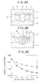
- FIG. 8(a) illustrates an interlayer dielectric film structure according to the prior art.
- those components which are the same as their counterparts of the above examples are indicated by the same reference numerals.
- Fig. 8(b) illustrates the manner in which the jut-out ratio of the low dielectric constant body in an interlayer dielectric film structure according to the invention is found.
- those components which are the same as their counterparts of the above examples are indicated by the same reference numerals. Plotted on the vertical axis of Fig.
- a plurality of conductive interconnects 14 are formed to a thickness of 600 nm over the lower dielectric layer 13 made of silicon oxide and having a relative dielectric constant of 4.0.
- a silicon oxide film 31 having a thickness of 200 nm and a relative dielectric constant of 4.0 is formed over the conductive interconnects 14.
- the lower dielectric layers 13 which are located on both sides and over which the conductive interconnects 14 are formed are lower by 200 nm than those portions in which the conductive interconnects 14 are formed.
- the second dielectric film 16 consisting of a low dielectric constant substance polyimide (relative dielectric constant is approximately equal to 3.0) is formed on both sides of the conductive interconnects 14 and the silicon oxide film 31.
- the upper dielectric layer 17 having a relative dielectric constant of 4.0 is formed over the silicon oxide film 31 and over the second dielectric film 16.
- the upper dielectric layer 17 is formed by plasma CVD, using tetraethoxysilane as a raw material. In this way, an interlayer dielectric film is formed by the second dielectric film 16, the silicon oxide film 31, and the upper dielectric film 17.
- the conductive interconnects 14 having a height of b are formed over the lower dielectric layer 13 having a relative dielectric constant of 4.0.
- the second dielectric film 16 consisting of a low dielectric substance and having a height of a is formed between the conductive interconnects 14.
- the upper dielectric layer 17 having a relative dielectric constant of 4.0 is formed over the conductive interconnects 14 and over the second dielectric film 16.
- the first dielectric film described in the above examples is not shown in this figure.
- the calculated film thickness of the second dielectric film includes the film thicknesses of the fourth and fifth dielectric films.
- the jut-out ratio R is in the range from 0.1 to 0.3. This shows that the capacitance between the conductive interconnects is reduced by at least 4-7% compared with the prior art structure.
- the reduction ratio of the converted capacitance between the conductive interconnects of the third and fourth examples described above is about half the reduction ratio of the converted capacitance of the fifth example.
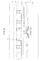
- Fig. 9 An example in which the fifth example of the invention is applied to an ordinary polycide gate MOS transistor is described by referring to Fig. 9.
- Fig. 9 the structure of Fig. 9 is compared with the structure of Fig. 7 which is a schematic cross section of the fifth example of the invention.
- the polycide gate MOS transistor corresponds to the semiconductor substrate 12 shown in Fig. 7.
- the method of fabricating the polycide gate MOS transistor is not described herein.
- the silicon oxide film 13 formed on the surface of the polycide gate MOS transistor corresponds to the lower oxide film 13 shown in Fig. 7.
- the fourth dielectric film 22 of a low dielectric constant is formed on the silicon oxide film 13.
- the third dielectric film 21 is formed on the fourth dielectric film 22.
- aluminum is deposited. This aluminum film is patterned, making use of a photolithography step and an etching step. Thus, the conductive interconnects 14 are formed.
- the first dielectric film 15 is formed and the second dielectric film 16 is buried on the principle of the fifth example of the invention. This is followed by formation of the fifth dielectric film 23 and the upper dielectric layer 17. The manner in which these films are formed has been already described in the fifth example.
Abstract
Description
- The present invention relates to a semiconductor device having high-density conductive interconnects and, more particularly, to a semiconductor device structure for realizing low electric power consumption and high-speed operation.
- As a means for accomplishing reductions in semiconductor device size, reductions in electric power consumption, and increases in operation speed, making lower the dielectric constants of interlayer dielectric films has been proposed. One example of this is disclosed in Japanese Patent Laid-Open No. 7650/1988 (Laid-Open Date: Jan. 13, 1988). In particular, a dielectric film between conductive interconnects is made from a low dielectric constant material having a relative dielectric constant smaller than that of dielectric films formed, respectively, over and under the conductive interconnects. Furthermore, in this structure, the dielectric film which is located between the conductive interconnects and has a low relative dielectric constant is in direct contact with the conductive interconnects.
- Often, the aforementioned low dielectric constant material consists of a dielectric film to which carbon is added to reduce the dielectric constant down to about 1.5 to 2.5. Alternatively, an organic material such as polyimide, poly-paraxylylene, or polysiloxane is used. Fabrication of semiconductor devices of the interlayer dielectric film structure using these materials has been discussed.
- A known method of fabricating a semiconductor device which has an interlayer dielectric film in direct contact with conductive interconnects is described by referring to the schematic cross sections of Figs. 1(a)-1(c). The interlayer dielectric film is made of a low dielectric constant material containing carbon. In Fig. 1(a), the dielectric film, indicated by 13, is formed on a
semiconductor substrate 12.Metallization 14 is deposited as a film on thedielectric film 13. Thedielectric film 13 of SiO₂ is formed to a thickness of about 0.5 µm by CVD, sputtering, or other techniques. Themetallization 14 is aluminium (Al) having a small specific resistance and deposited to a thickness of about 0.5 µm. - The state shown in Fig. 1(b) is obtained by forming a resist pattern by a lithographic method (not shown) and then etching the
dielectric film 13 and themetallization 14 at the same time by a dry etching process. In the dry etching process, CCl₄ is normally used to etch the Al. Mixture of CF₄ and H₂ or other material is employed to etch the dielectric film of SiO₂. - In the state shown in Fig. 1(c), a
dielectric film 16 having a relative dielectric constant smaller than that of thedielectric film 13 is buried. Thisdielectric film 16 consists of polytetrafluoroethylene, polyethylene, or the like. - However, the dielectric film which is used in the prior art techniques and made from a low dielectric constant material containing carbon shows hygroscopicity and so the moisture resistance is poor. Therefore, especially in aluminium interconnects, corrosion takes place, thus deteriorating the reliability of the finished semiconductor device. Furthermore, the plasma resistance is not satisfactory. Especially, the dielectric film is vulnerable to oxygen plasma. Hence, it is difficult to use this dielectric film as an interlayer dielectric film in a semiconductor device.
- It is a first object of the present invention to provide an interlayer dielectric film structure which is for use in a semiconductor device and which permits a low dielectric constant film having neither excellent hygroscopicity nor excellent plasma resistance to be used as an interlayer dielectric film and which improves the reliability of conductive interconnects. It is an additional object of the invention to provide an interlayer dielectric film structure which is for use in a semiconductor device and which accomplishes low electric power consumption and high-speed operation with high-density conductive interconnects.
- The present invention provides an interlayer dielectric film structure which is for use in a semiconductor device which has a main body, a first dielectric film, and a second dielectric film formed at least between conductive interconnects. The main body is used for fabricating a semiconductor device. At least the surface of the main body is insulative. The first dielectric film is formed on the main body so as to cover the conductive interconnects formed over the main body and separate those interconnects from the second dielectric film. The second dielectric film has a relative dielectric constant smaller than that of the first dielectric film.
- Certain embodiments of the invention provide an interlayer dielectric film structure which is similar to the structure described in the immediately preceding paragraph but which is further characterized in that the thickness of the second dielectric film is larger than the height of the conductive interconnects by 10-100% in the directions of the height and depth.
- Further embodiments of the invention provide an interlayer dielectric film structure which is similar to the structure described in the immediately preceding paragraph but which is further characterized in that a third dielectric film having substantially the same relative dielectric constant as the first dielectric film is formed under the conductive interconnects, and that a fourth dielectric film having a thickness of 10-30% of the height of the conductive interconnects and having substantially the same relative dielectric constant as the second dielectric film is formed under the third dielectric film.
- Yet further embodiments of the invention provide an interlayer dielectric film structure which is characterized in that the above-described third dielectric film consists of at least one of silicon oxide, silicon oxynitride, and silicon nitride, and that the fourth dielectric film consists of at least one of silicon oxide, silicon oxide containing fluorine, polysiloxane materials, parylene, fluorocarbon materials, and polyimide materials.
- Still further embodiments of the invention provide an interlayer dielectric film structure which is characterized in that a fifth dielectric film is formed over the above-described conductive interconnects via the first dielectric film, and that the fifth dielectric film consists of at least one of silicon oxide, silicon oxide containing fluorine, polysiloxane materials, polyparaxylylene, fluorocarbon materials, and polyimide materials. This structure is further characterized in that the thickness of the fifth dielectric film is more than 10% and less than 30% of the height of the conductive interconnects and has substantially the same relative dielectric constant as the second dielectric film.
- Various embodiments of the invention provide an interlayer dielectric film structure which is for use in a semiconductor device and which is characterized in that a plurality of first dielectric films of the structure described above are formed, and that each of the first dielectric films consists of at least one of silicon oxide, silicon oxynitride, and silicon nitride.
- Still further embodiments of the invention provide an interlayer dielectric film structure which is for use in a semiconductor device and which is characterized in that a plurality of second dielectric films of the structure described above are formed and each second dielectric film consists of at least one of silicon oxide, silicon oxide containing fluorine, polysiloxane materials, polyparaxylylene, fluorocarbon materials, and polyimide materials.
- In these interlayer dielectric film structures for use in semiconductor devices, the first dielectric film is formed so as to cover the conductive interconnects. Therefore, the conductive interconnects are protected from corrosion and poisoning by the second dielectric film of low dielectric constant. Furthermore, the second dielectric film having a relative dielectric constant smaller than that of the first dielectric film is formed at least between the conductive interconnects and so the capacitance between the conductive interconnects decreases. In this way, a semiconductor device structure and a fabrication method which accomplish low electric power consumption and high-speed operation with high-density conductive interconnects are disclosed.
- Other objects and features of the invention will appear in the course of the description thereof, which follows.
-
- Fig. 1(a) is a cross-sectional view of the prior art structure obtained when a
dielectric film 13 andmetallization 14 are deposited over a semiconductor substrate; - Fig. 1(b) is a cross-sectional view similar to Fig. 1(a), but in which a dry etching process has been performed after the
dielectric film 13 and themetallization 14 over the semiconductor substrate have been patterned with a resist; - Fig. 1(c) is a cross-sectional view similar to Fig. 1(b), but in which a
dielectric film 16 having a relative dielectric constant smaller than that of thedielectric film 13 has been buried; - Fig. 2 is a schematic cross-sectional view of the structure of a first example of the present invention;
- Fig. 3 is a schematic cross-sectional view of the structure of a second example of the invention;
- Fig. 4 is a schematic cross-sectional view of the structure of a third example of the invention;
- Fig. 5(a) is a cross-sectional view illustrating one fabrication process of the third example of the invention, and in which dielectric films and metallization have been deposited;
- Fig. 5(b) is a cross-sectional view similar to Fig. 5(a), but in which the side walls of conductive interconnects have been coated with a
dielectric film 15 after the dielectric films and metallization have been patterned; - Fig. 5(c) is a cross-sectional view similar to Fig. 5(b), but in which an upper
dielectric film 17 has been deposited after spaces between the conductive interconnects are provided with a material having a low dielectric constant; - Fig. 6 is a schematic cross-sectional view of the structure of a fourth example of the invention;
- Fig. 7 is a schematic cross-sectional view of the structure of a fifth example of the invention;
- Fig. 8(a) is a cross-sectional view of the prior art interlayer dielectric film structure, illustrating the effect of reduction of the capacitance between conductive interconnects;
- Fig. 8(b) is a cross-sectional view similar to Fig. 8(a), but illustrating the manner in which a jut-out ratio of the low dielectric electric constant material in an interlayer dielectric film structure according to the invention is found;
- Fig. 8(c) is a graph comparing the effect of reduction of the capacitance between conductive interconnects obtained by the present invention with the effect of reduction of the capacitance between conductive interconnects obtained by the prior art interlayer dielectric film structure; and
- Fig. 9 is a schematic cross-sectional view of a semiconductor device to which the fifth example of the invention is applied.
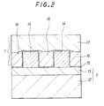
- A first example of the present invention is now described by referring to the schematic cross section of Fig. 2.
- As shown in Fig. 2, a base or
main body 11 comprises asemiconductor substrate 12, for example, on which a lowerdielectric layer 13 consisting of silicon oxide (e.g., having a relative dielectric constant of 4.0) is formed. For example, a plurality ofconductive interconnects 14 are formed over the lowerdielectric layer 13 of thebase 11. - A
first dielectric film 15 is formed so as to cover theconductive interconnects 14. This firstdielectric film 15 is made of silicon oxide (e.g., having a relative dielectric constant of 4.0) having a film thickness of 2 nm. Alternatively, the film is made of silicon oxynitride (e.g., having a relative dielectric constant of 4.0-6.0) or silicon nitride (e.g., having a relative dielectric constant of 6.0). - A
second dielectric film 16 having a relative dielectric constant smaller than that of thefirst dielectric film 15 is formed between theconductive interconnects 14 via thefirst dielectric film 15. Also, thesecond dielectric film 16 is formed over the lowerdielectric layer 13 which is on one side of theconductive interconnects 14. In the present figure, thesecond dielectric film 16 is formed over the lowerdielectric layer 13 via thefirst dielectric film 15 but thesecond dielectric film 16 may be formed directly on the lowerdielectric layer 13. That is, it is only necessary that thefirst dielectric layer 15 be present at least between eachconductive interconnect 14 and thesecond dielectric film 16. - The aforementioned
second dielectric film 16 may be made of polysiloxane based polymer (e.g., having a relative dielectric constant of 2.8). Alternatively, the film may be made of silicon oxide containing fluorine atoms (e.g., having a relative dielectric constant of 3.0) or polyimide consisting of a polyimide material (e.g., having a relative dielectric constant of 3.0), or other suitable materials of low relative dielectric constant. - An
upper dielectric layer 17 consisting, for example, of silicon oxide (e.g., having a relative dielectric constant of 4.0) is formed over the first and seconddielectric films - As mentioned previously, the
interlayer dielectric film 1 is formed by the first and seconddielectric films upper dielectric layer 17 so as to cover theconductive interconnects 14. - A method of fabricating the above-described interlayer dielectric film structure is briefly described. The
conductive interconnects 14 are formed over thesemiconductor substrate 12 by ordinary conductive interconnect formation techniques. The lowerdielectric layer 13 is formed on the front surface of thesubstrate 12. Then, thefirst dielectric film 15 is formed over the lowerdielectric layer 13 so as to cover the surfaces of theconductive interconnects 14, for example, by ECR (electron cyclotron resonance) CVD. As one example of the film formation conditions, silane (SiH₄) and nitrous oxide (N₂O) are used as reactant gases. Nitrogen (N₂) is used as a carrier gas. The RF power is set to 500 W. The substrate temperature is set to 400°C. - After forming the
first dielectric film 15 under these conditions, a polysiloxane based polymer is applied to form thesecond dielectric film 16. The polymer given by Eq. (1) is used as this polysiloxane based polymer.
- Then, the
second dielectric film 16 is etched back, for example by ECR etching, until thefirst dielectric film 15 over theconductive interconnects 14 is exposed. As a result, thesecond dielectric film 16 exists at least between theconductive interconnects 14. Thereafter, theupper dielectric layer 17 is formed out of silicon oxide over the first and seconddielectric films - In the above-described interlayer dielectric film structure for a semiconductor device, the
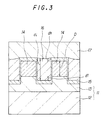
first dielectric film 15 is formed so as to cover theconductive interconnects 14 and so theinterconnects 14 are protected from corrosion and poisoned vias due to the second dielectric film of low dielectric constant. Furthermore, since thesecond dielectric film 16 of a relative dielectric constant lower than that of thefirst dielectric film 15 is formed at least between theconductive interconnects 14, the electric field set up by the conductive interconnects passes through thesecond dielectric film 16 of low dielectric constant. Therefore, the capacitance between theconductive interconnects 14 is reduced. - A second example is next described by referring to the schematic cross section of Fig. 3. In this figure, those components which are the same as their counterparts of Fig. 2 are indicated by the same reference numerals.
- As shown in Fig. 3, this interlayer dielectric film structure is similar to the structure shown in Fig. 2 except that the thickness of the
second dielectric film 16 is larger than the height of theconductive interconnects 14 by 10-100% in the directions of the height and depth. That is, of the thickness di of thesecond dielectric film 16, the thickness dh of the portion higher than theconductive interconnects 14 and the thickness dl of the portion lower than theconductive interconnects 14 are set to 10-100% of the height D of theconductive interconnects 14. - In the same manner as described already in the first example, the base or
main body 11 consists of thesemiconductor substrate 12 having the lowerdielectric layer 13 formed on its surface. Thefirst dielectric film 15 is formed so as to cover theconductive interconnects 14. Theupper dielectric layer 17 is formed over the first and seconddielectric films - The method of fabrication of the interlayer dielectric film structure of the above-described second example is carried out by the same process as described in the first example. However, the difference with the process of the first example is that when the
conductive interconnects 14 are patterned by etching, the lowerdielectric layer 13 is also etched. The etching depth of the lowerdielectric layer 13 is determined in the manner described below. Let de be the etching depth of the lowerdielectric layer 13. Let dl be the thickness of thefirst dielectric film 15 which will be deposited later over the etched portions in the lowerdielectric layer 13. Let D be the height of theconductive interconnects 14. The lowerdielectric layer 13 is so etched that the relation de - dl = 0,1D to 1.0D holds. - ECR (electron cyclotron resonance) CVD is used to form the
first dielectric film 15. Thefirst dielectric film 15 is deposited over the etched portions in the lowerdielectric layer 13 and over theconductive interconnects 14 to a thickness larger than side walls of theconductive interconnects 14. - In the second example, the thickness of the
second dielectric film 16 between theconductive interconnects 14 is larger than the height D of theconductive interconnects 14 by 10-100% in the directions of the height and depth. Therefore, the capacitance between theconductive interconnects 14 is made lower than in the first example, because the electric field generated by theconductive interconnects 14 can pass more easily. - If the excessive thick portion is less than 10%, the path of the electric field produced by the
conductive interconnects 14 is not limited to thesecond dielectric film 16. Therefore, capacitance is created between theconductive interconnects 14. This makes it impossible to sufficiently lower the capacitance. On the other hand, if the excessive portion is greater than 100%, the step becomes steep. In consequence, the burying characteristics of thesecond dielectric film 16 are deteriorated in the latter situations. Accordingly, the thickness amount is set to the above-described range. - A third example is next described by referring to the schematic cross section of Fig. 4. In this figure, those components which are the same as their counterparts of Fig. 2 are indicated by the same reference numerals.
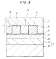
- As shown in Fig. 4, this interlayer dielectric film structure is similar to the structure shown in Fig. 2 except that a
third dielectric film 21 and afourth dielectric film 22 are formed under theconductive interconnects 14. This thirddielectric film 21 has substantially the same relative dielectric constant as the first dielectric film. Examples of the material include silicon oxide, silicon oxynitride, and silicon nitride. On the other hand, the thickness of thefourth dielectric film 22 is more than 10% and less than 30% of the height of theconductive interconnects 14. Thefourth dielectric film 22 has substantially the same relative dielectric constant as thesecond dielectric film 16 as described previously in the first example. This fourthdielectric film 22 consists of at least one of silicon oxide containing fluorine, polysiloxane materials, polyparaxylylene, fluorocarbon materials, and polyimide materials. - This structure is similar to the structure already described in connection with Fig. 2 in other respects. That is, the base or
main body 11 consists of thesemiconductor substrate 12 having the lowerdielectric layer 13 formed on its surface. Theconductive interconnects 14 are formed over the lowerdielectric layer 13 via the fourth and thirddielectric films first dielectric film 15 is formed so as to cover theconductive interconnects 14. Theupper dielectric layer 17 is formed over the first and seconddielectric films interlayer dielectric film 1 is constructed in this way. - In the above-described structure, of the
first dielectric film 15 and thethird dielectric film 21 between theconductive interconnects 14, those portions which are not in direct contact with theconductive interconnects 14 are not required to be formed. Therefore, thefirst dielectric film 15 and thethird dielectric film 21 may be formed so as to surround theconductive interconnects 14. - The method of fabrication of the interlayer dielectric film structure of the above-described third example is carried out by a process similar to the process previously described in the first example. However, the difference with the process of the first example is that the
fourth dielectric film 22 and thethird dielectric film 21 are successively stacked over the lowerdielectric layer 13 before theconductive interconnects 14 are formed. First, by the spin coating, thefourth dielectric film 22 is applied over the lowerdielectric layer 13 to a film thickness of 100 nm. Subsequently, thethird dielectric film 21 is formed to a film thickness, for example, of 10 nm by ECR CVD. Then, theconductive interconnects 14 are formed by metallization formation techniques, followed by execution of the process already described in the first example. - It is also possible to fabricate the inter-layer dielectric film structure of the third example by a different process. This process is characterized in that the first and fourth dielectric films on that portion of the fourth dielectric film which is between the conductive interconnects are removed.
- In particular, as shown in Fig. 5(a), before the
conductive interconnects 14 are formed, afourth dielectric film 22 is formed over the lowerdielectric layer 13 of thebase 11, for example, to a film thickness of 100 nm by an application method. Then, athird dielectric film 21 is formed, for example, to a film thickness of 10 nm by ECR CVD. Subsequently, ametallization film 31 for forming theconductive interconnects 14 are formed by sputtering. Then, a dielectric film 32 (which, in the finished product, is the first dielectric film 15) is formed on themetallization film 31 by CVD. - Then, a patterning step using ordinary lithography and etching techniques is carried out to form the
conductive interconnects 14 from themetallization film 31 as shown in Fig. 5(b). At this time, the dielectric film 32 (later becoming the first dielectric film 15) is left over theconductive interconnects 14. Thethird dielectric film 21 at positions between theconductive interconnects 14 is etched away. - Thereafter, side walls 33 (becoming the first dielectric film 15) are formed on the side walls of the
conductive interconnects 14 by ordinary side wall formation techniques making use of formation of a further dielectric film (not shown) for the side walls and etch-back. Of course, the further dielectric film lying between theconductive interconnects 14 is removed during the etch-back for forming theside walls 33. The further dielectric film overlying theconductive interconnects 14 and used for the side walls is also removed. However, at least the bottom portion of thedielectric film 32 remains. Therefore, theconductive interconnects 14 are covered with thefirst dielectric film 15 consisting of thedielectric film 32 left on theconductive interconnects 14 and theside walls 33. - Thereafter, the process described in the first example is carried out to form the
second dielectric film 16 and theupper dielectric layer 17 as shown in Fig. 5(C). - If the interlayer dielectric film structure is formed by the process described above, the
second dielectric film 16 is directly connected with thefourth dielectric film 22. - In the above-described third example, the
third dielectric film 21 and thefourth dielectric film 22 are formed under theconductive interconnects 14 and so thethird dielectric film 21 having substantially the same relative dielectric constant as thefirst dielectric film 15 protects theconductive interconnects 14 from corrosion and poisoned vias due to thefourth dielectric film 22 of low dielectric constant. Because the thickness of thefourth dielectric film 22 is more than 10% and less than 30% of the height of theconductive interconnects 14, and because thefourth dielectric film 22 has substantially the same relative dielectric constant as thesecond dielectric film 16, the electric field produced by theconductive interconnects 14 passes through thefourth dielectric film 22 of low dielectric constant. Consequently, the capacitance between theconductive interconnects 14 is reduced. - If the thickness of the
fourth dielectric film 22 is lower than 10% of the height of theconductive interconnects 14, the electric field developed by theconductive interconnects 14 hardly passes through thefourth dielectric film 22 but passes through the lowerdielectric layer 13. Consequently, the capacitance is reduced less efficiently. On the other hand, if the thickness is in excess of 30%, the moisture resistance is adversely affected, because the film quality of thefourth dielectric film 22 is poor. When a thermal step is effected, if thefourth dielectric film 22 contains carbon, hydrocarbon gases are produced. This renders the film porous. For this reason, the moisture resistance is further deteriorated. Accordingly, the film thickness of thefourth dielectric film 22 is set to the above-described range. - A fourth example is next described by referring to the schematic cross section of Fig. 6. In this figure, those components which are the same as their counterparts of Fig. 2 are indicated by the same reference numerals.
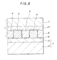
- As shown in Fig. 6, this interlayer dielectric film structure is similar to the structure shown in Fig. 2 except that a
fifth dielectric film 23 is formed over theconductive interconnects 14 via thefirst dielectric film 15. In this example, thefifth dielectric film 23 is formed also over thesecond dielectric film 16. The thickness of thefifth dielectric film 23 is more than 10% and less than 30% of the height of theconductive interconnects 14. Thefifth dielectric film 23 has substantially the same relative dielectric constant as thesecond dielectric film 16 described in the first example. Thefifth dielectric film 23 consists, for example, of at least one of silicon oxide containing fluorine, polysiloxane materials, polyparaxylylene, fluorocarbon materials, and polyimide materials. - For instance, where the height of the
conductive interconnects 14 is 600 nm, thefifth dielectric film 23 is formed to a film thickness of 100 nm, for example. In this case, it accounts for about 17% of the film thickness of theconductive interconnects 14. The structure is the same as the structure described already in connection with Fig. 2 in other respects. - That is, the base or
main body 11 consists of thesemiconductor substrate 12 having the lowerdielectric layer 13 formed on its surface. Theconductive interconnects 14 are formed over the lowerdielectric layer 13. Thefirst dielectric film 15 is formed so as to cover theconductive interconnects 14. Theupper dielectric layer 17 is formed over the first and seconddielectric films fifth dielectric layer 23. Theinterlayer dielectric film 1 is constructed in this way. - The method of fabrication of the interlayer dielectric film structure of the above-described fourth example is carried out by a process similar to the process described in the first example. However, the difference with the process of the first example is that the
second dielectric film 16 is left over theconductive interconnects 14 via thefirst dielectric film 15 when thesecond dielectric film 16 is etched back. That is, thesecond dielectric film 16 is left up to a thickness which is more than 10% and less than 30% of the height of theconductive interconnects 14. The left seconddielectric film 16 becomes thefifth dielectric film 23. Therefore, thefifth dielectric film 23 consists of a polysiloxane based polymer, in the same way as thesecond dielectric film 16. Alternatively, the fifth film is made of silicon oxide containing fluorine carbon, poly-paraxylylene, a fluorocarbon material, or a polyimide material such as polyimide. - In the fourth example described above, the
fifth dielectric film 23 is formed over theconductive interconnects 14 via thefirst dielectric film 15 and so theconductive interconnects 14 are protected from corrosion and poisoned vias due to thefifth dielectric film 23 of low dielectric constant. Because the thickness of the height of the conductive interconnects is more than 10% and less than 30% of the height of the conductive interconnects, and because thefifth dielectric film 23 having substantially the same relative dielectric constant as thesecond dielectric film 16 is formed, the electric field generated by theconductive interconnects 14 passes through thefifth dielectric film 23 of low dielectric constant. In consequence, the capacitance between theconductive interconnects 14 is reduced. - If the thickness of the
fifth dielectric film 23 is lower than 10% of the height of theconductive interconnects 14, the electric field developed by theconductive interconnects 14 hardly passes through thefifth dielectric film 23 but passes through theupper dielectric layer 17. Consequently, the capacitance is reduced less efficiently. On the other hand, if the thickness is in excess of 30%, the moisture resistance is adversely affected, because the film quality of thefifth dielectric film 23 is poor. When a thermal step is effected, if thefifth dielectric film 23 contains carbon, hydrocarbon gases are produced. This renders the film porous. For this reason, the moisture resistance is further deteriorated. Accordingly, the film thickness is set to the above-described range. - A fifth example which is a combination of the third example and the fourth example described above is next described by referring to the schematic cross section of Fig. 7. In this figure, those components which are the same as their counterparts of Figs. 4 and 6 are indicated by the same reference numerals.
- As shown in Fig. 7, this interlayer dielectric film structure combines the structure shown in Fig. 4 with the structure shown in Fig. 6. That is, a
fourth dielectric film 22 and athird dielectric film 21 are formed over the lowerdielectric layer 13 of thebase 11.Conductive interconnects 14 are formed over thethird dielectric film 21. Therefore, thethird dielectric film 21 and thefourth dielectric film 22 are formed under theconductive interconnects 14. - The
third dielectric film 21 is made of a material having substantially the same relative dielectric constant as thefirst dielectric film 15, e.g., silicon oxide, silicon oxynitride, or silicon nitride. The thickness of thefourth dielectric film 22 is more than 10% and less than 30% of the height of theconductive interconnects 14. Thefourth dielectric film 22 has substantially the same relative dielectric constant as thesecond dielectric film 16 described in the first example. This fourthdielectric film 22 consists, for example, of at least one of silicon oxide containing fluorine, polysiloxane materials, polyparaxylylene, fluorocarbon materials, and polyimide materials. - The
conductive interconnects 14 are coated with thefirst dielectric film 15. Thesecond dielectric film 16 similar to that described in the first example is formed between theconductive interconnects 14 via thefirst dielectric film 15 similar to that described in the first example. Afifth dielectric film 23 is formed over theconductive interconnects 14 via thefirst dielectric film 15. This fifthdielectric film 23 is formed also over thesecond dielectric film 16. - The thickness of the
fifth dielectric film 23 is more than 10% and less than 30% of the height of theconductive interconnects 14. Thefifth dielectric film 23 has substantially the same relative dielectric constant as thesecond dielectric film 16. This fifthdielectric film 23 consists, for example, of at least one of silicon oxide containing fluorine, polysiloxane materials, polyparaxylylene, fluorocarbon materials, and polyimide materials. - The
upper dielectric layer 17 consisting, for example, of silicon oxide is formed over thefifth dielectric film 23. Theinterlayer dielectric film 1 is constructed in this way. - For instance, where the height of the
conductive interconnects 14 is 600 nm, thethird dielectric film 21 is formed to a film thickness of 10 nm, for example. Thefourth dielectric film 22 is formed to a film thickness of 100 nm. Thefifth dielectric film 23 is formed to a film thickness of 100 nm. In this case, the film thicknesses of the fourth and fifthdielectric films conductive interconnects 14. - In the method of fabricating the interlayer dielectric film structure of the fifth example, the
fourth dielectric film 22, thethird dielectric film 21, and theconductive interconnects 14 are formed by a process similar to the process described in the third example. Then, thefirst dielectric film 15 is formed. Thereafter, thesecond dielectric film 16 and thefifth dielectric film 23 are formed integrally by a process similar to the process described in the fourth example. Subsequently, theupper dielectric layer 17 is formed. - In the above-described fifth example, the
fourth dielectric film 22 is formed under theconductive interconnects 14 via thethird dielectric film 21. Thesecond dielectric film 16 is formed over theconductive interconnects 14 via thefirst dielectric film 15. Consequently, the capacitance between theconductive interconnects 14 is made lower than in the third and fourth examples. - The effect of reduction of the capacitance between the conductive interconnects is next described by referring to Figs. 8(a)-8(c). Fig. 8(a) illustrates an interlayer dielectric film structure according to the prior art. In this figure, those components which are the same as their counterparts of the above examples are indicated by the same reference numerals. Fig. 8(b) illustrates the manner in which the jut-out ratio of the low dielectric constant body in an interlayer dielectric film structure according to the invention is found. In this figure, those components which are the same as their counterparts of the above examples are indicated by the same reference numerals. Plotted on the vertical axis of Fig. 8(c) is converted capacitance when the conductive interconnects (aluminum interconnects, in this example) are coated with a dielectric film having a relative dielectric constant of 2.5 and when the capacitance between the conductive interconnects is taken as 100%. Plotted on the horizontal axis is the jut-out ratio of the low dielectric constant body.
- First, the prior art interlayer dielectric structure is described. As shown in Fig. 8(a), a plurality of
conductive interconnects 14 are formed to a thickness of 600 nm over the lowerdielectric layer 13 made of silicon oxide and having a relative dielectric constant of 4.0. Asilicon oxide film 31 having a thickness of 200 nm and a relative dielectric constant of 4.0 is formed over theconductive interconnects 14. The lowerdielectric layers 13 which are located on both sides and over which theconductive interconnects 14 are formed are lower by 200 nm than those portions in which theconductive interconnects 14 are formed. Thesecond dielectric film 16 consisting of a low dielectric constant substance polyimide (relative dielectric constant is approximately equal to 3.0) is formed on both sides of theconductive interconnects 14 and thesilicon oxide film 31. Theupper dielectric layer 17 having a relative dielectric constant of 4.0 is formed over thesilicon oxide film 31 and over thesecond dielectric film 16. Theupper dielectric layer 17 is formed by plasma CVD, using tetraethoxysilane as a raw material. In this way, an interlayer dielectric film is formed by thesecond dielectric film 16, thesilicon oxide film 31, and theupper dielectric film 17. - The manner in which the jut-out ratio of the low dielectric constant body of an interlayer dielectric film structure according to the invention is found is next described. As shown in Fig. 8(b), the
conductive interconnects 14 having a height of b are formed over the lowerdielectric layer 13 having a relative dielectric constant of 4.0. Thesecond dielectric film 16 consisting of a low dielectric substance and having a height of a is formed between theconductive interconnects 14. Theupper dielectric layer 17 having a relative dielectric constant of 4.0 is formed over theconductive interconnects 14 and over thesecond dielectric film 16. The first dielectric film described in the above examples is not shown in this figure. - The jut-out ratio R of the
second dielectric film 16 relative to theconductive interconnects 14 is calculated to be R = (a - b) /2b. - Where the fourth and fifth dielectric films becoming a low dielectric constant body described in the third, fourth, and fifth examples are formed over or under the
conductive interconnects 14, the calculated film thickness of the second dielectric film includes the film thicknesses of the fourth and fifth dielectric films. - The results of the calculated capacitance between the conductive interconnects are described with reference to Fig. 8(c), where the converted capacitance of the prior art interlayer dielectric film structure shown in Fig. 8(a) is indicated by the broken line, while the converted capacitance of the structure of the fifth example is indicated by the solid line.
- As shown, in the structure of the fifth example where the fourth and fifth dielectric films of a low dielectric constant substance are formed under and over the conductive interconnects, the jut-out ratio R is in the range from 0.1 to 0.3. This shows that the capacitance between the conductive interconnects is reduced by at least 4-7% compared with the prior art structure.
- Although not illustrated, the reduction ratio of the converted capacitance between the conductive interconnects of the third and fourth examples described above is about half the reduction ratio of the converted capacitance of the fifth example.
- An example in which the fifth example of the invention is applied to an ordinary polycide gate MOS transistor is described by referring to Fig. 9. For simplicity, the structure of Fig. 9 is compared with the structure of Fig. 7 which is a schematic cross section of the fifth example of the invention.
- In Fig. 9, the polycide gate MOS transistor corresponds to the
semiconductor substrate 12 shown in Fig. 7. The method of fabricating the polycide gate MOS transistor is not described herein. Thesilicon oxide film 13 formed on the surface of the polycide gate MOS transistor corresponds to thelower oxide film 13 shown in Fig. 7. Thefourth dielectric film 22 of a low dielectric constant is formed on thesilicon oxide film 13. Thereafter, thethird dielectric film 21 is formed on thefourth dielectric film 22. Subsequently, in order to form the plural Al interconnects 14, aluminum is deposited. This aluminum film is patterned, making use of a photolithography step and an etching step. Thus, theconductive interconnects 14 are formed. - Then, the
first dielectric film 15 is formed and thesecond dielectric film 16 is buried on the principle of the fifth example of the invention. This is followed by formation of thefifth dielectric film 23 and theupper dielectric layer 17. The manner in which these films are formed has been already described in the fifth example.
Claims (8)
- An interlayer dielectric film structure (1) for a semiconductor device, comprising:a substrate (11) made from a semiconductor material;said semiconductor device fabricated from said substrate by semiconductor fabrication processes;a main body formed by said semiconductor device and comprising a first dielectric film (15) and a second dielectric film (16), at least a surface of said main body being insulative;conductive interconnects (14) formed on said main body;said first dielectric film (15) being formed so as to cover said conductive interconnects; andsaid second dielectric film (16) having a relative dielectric constant smaller than that of said first dielectric film, said second dielectric film existing at least between said conductive interconnects (14) but separated therefrom by said first dielectric film (15).
- The interlayer dielectric film structure of claim 1, wherein said second dielectric film (16) between said conductive interconnects (14) has a thickness larger than height (D) of the conductive interconnects by 10 to 100% in directions of height and depth.
- The interlayer dielectric film structure of claim 1, further comprising:a third dielectric film (21) having substantially the same relative dielectric constant as said first dielectric film (15) and formed under said conductive interconnects (14); anda fourth dielectric film (22) having a thickness that is more than 10% and less than 30% of the height (D) of said conductive interconnects (14), said fourth dielectric film (22) having substantially the same relative dielectric constant as said second dielectric film (16), said fourth dielectric film (22) being formed under said third dielectric film (21).
- The interlayer dielectric film structure of claim 3, wherein said third dielectric film (21) consists of at least one of silicon oxide, silicon oxynitride, and silicon nitride, and wherein said fourth dielectric film (22) consists of at least one of silicon oxide containing fluorine, polysiloxane materials, polyparaxylylene, fluorocarbon materials, and polyimide materials.
- The interlayer dielectric film structure of any previous claim, further comprising a fifth dielectric film (23) having a thickness which is more than 10% and less than 30% of the height (D) of said conductive interconnects (14), said fifth dielectric film (23) having substantially the same relative dielectric constant as said second dielectric film (16), said fifth dielectric film (23) being formed over said conductive interconnects (14) via said first dielectric film (15).
- The interlayer dielectric film structure of claim 5, wherein said fifth dielectric film (23) consists of at least one of silicon oxide containing fluorine, polysiloxane materials, polyparaxylylene, fluorocarbon materials, and polyimide materials.
- The interlayer dielectric film structure of any previous claim, wherein said first dielectric film (15) consists of at least one of silicon oxide, silicon oxynitride, and silicon nitride.
- The interlayer dielectric film structure of any previous claim, wherein said second dielectric film (16) consists of at least one of silicon oxide containing fluorine, polysiloxane materials, polyparaxylylene, fluorocarbon materials, and polyimide materials.
Applications Claiming Priority (4)
| Application Number | Priority Date | Filing Date | Title |
|---|---|---|---|
| JP238821/94 | 1994-10-03 | ||
| JP23882194 | 1994-10-03 | ||
| JP3727/95 | 1995-01-13 | ||
| JP7003727A JPH08162528A (en) | 1994-10-03 | 1995-01-13 | Interlayer insulating film structure of semiconductor device |
Publications (3)
| Publication Number | Publication Date |
|---|---|
| EP0706216A2 true EP0706216A2 (en) | 1996-04-10 |
| EP0706216A3 EP0706216A3 (en) | 1997-12-03 |
| EP0706216B1 EP0706216B1 (en) | 2007-05-30 |
Family
ID=26337363
Family Applications (1)
| Application Number | Title | Priority Date | Filing Date |
|---|---|---|---|
| EP95402206A Expired - Lifetime EP0706216B1 (en) | 1994-10-03 | 1995-10-03 | Interlayer dielectric structure for semiconductor device |
Country Status (5)
| Country | Link |
|---|---|
| US (1) | US5646440A (en) |
| EP (1) | EP0706216B1 (en) |
| JP (1) | JPH08162528A (en) |
| KR (1) | KR960015788A (en) |
| DE (1) | DE69535502T2 (en) |
Cited By (36)
| Publication number | Priority date | Publication date | Assignee | Title |
|---|---|---|---|---|
| FR2741192A1 (en) * | 1995-11-10 | 1997-05-16 | Samsung Electronics Co Ltd | DESIGN AND MANUFACTURING PROCESS OF INTEGRATED CIRCUITS AND INTEGRATED CIRCUITS MADE ACCORDING TO THIS PROCEDURE |
| EP0805491A2 (en) * | 1996-04-29 | 1997-11-05 | Texas Instruments Incorporated | Interconnect structure and method of manufacturing using two different low dielectric constant insulators |
| WO1997041592A1 (en) * | 1996-05-02 | 1997-11-06 | Advanced Micro Devices, Inc. | A fluorinated oxide low permittivity dielectric stack for reduced capacitive coupling |
| EP0851490A2 (en) * | 1996-12-25 | 1998-07-01 | Nec Corporation | Semiconductor device and process for production thereof |
| EP0851491A2 (en) * | 1996-12-25 | 1998-07-01 | Nec Corporation | Semiconductor device having multilevel interconnection structure and manufacturing method thereof |
| EP1094508A2 (en) | 1999-10-22 | 2001-04-25 | Lsi Logic Corporation | Void-free low K dielectric composite layer between metal lines in integrated circuit structure |
| EP1123991A2 (en) * | 2000-02-08 | 2001-08-16 | Asm Japan K.K. | Low dielectric constant materials and processes |
| US6346488B1 (en) | 2000-06-27 | 2002-02-12 | Lsi Logic Corporation | Process to provide enhanced resistance to cracking and to further reduce the dielectric constant of a low dielectric constant dielectric film of an integrated circuit structure by implantation with hydrogen ions |
| US6346490B1 (en) | 2000-04-05 | 2002-02-12 | Lsi Logic Corporation | Process for treating damaged surfaces of low k carbon doped silicon oxide dielectric material after plasma etching and plasma cleaning steps |
| US6350700B1 (en) | 2000-06-28 | 2002-02-26 | Lsi Logic Corporation | Process for forming trenches and vias in layers of low dielectric constant carbon-doped silicon oxide dielectric material of an integrated circuit structure |
| US6365528B1 (en) | 2000-06-07 | 2002-04-02 | Lsi Logic Corporation | Low temperature process for forming a low dielectric constant fluorine and carbon-containing silicon oxide dielectric-material characterized by improved resistance to oxidation and good gap-filling capabilities |
| US6368979B1 (en) | 2000-06-28 | 2002-04-09 | Lsi Logic Corporation | Process for forming trenches and vias in layers of low dielectric constant carbon-doped silicon oxide dielectric material of an integrated circuit structure |
| US6391768B1 (en) | 2000-10-30 | 2002-05-21 | Lsi Logic Corporation | Process for CMP removal of excess trench or via filler metal which inhibits formation of concave regions on oxide surface of integrated circuit structure |
| US6420277B1 (en) | 2000-11-01 | 2002-07-16 | Lsi Logic Corporation | Process for inhibiting crack formation in low dielectric constant dielectric films of integrated circuit structure |
| US6423628B1 (en) | 1999-10-22 | 2002-07-23 | Lsi Logic Corporation | Method of forming integrated circuit structure having low dielectric constant material and having silicon oxynitride caps over closely spaced apart metal lines |
| US6444564B1 (en) | 1998-11-23 | 2002-09-03 | Advanced Micro Devices, Inc. | Method and product for improved use of low k dielectric material among integrated circuit interconnect structures |
| US6489242B1 (en) | 2000-09-13 | 2002-12-03 | Lsi Logic Corporation | Process for planarization of integrated circuit structure which inhibits cracking of low dielectric constant dielectric material adjacent underlying raised structures |
| US6492731B1 (en) | 2000-06-27 | 2002-12-10 | Lsi Logic Corporation | Composite low dielectric constant film for integrated circuit structure |
| US6503840B2 (en) | 2001-05-02 | 2003-01-07 | Lsi Logic Corporation | Process for forming metal-filled openings in low dielectric constant dielectric material while inhibiting via poisoning |
| US6524974B1 (en) | 1999-03-22 | 2003-02-25 | Lsi Logic Corporation | Formation of improved low dielectric constant carbon-containing silicon oxide dielectric material by reaction of carbon-containing silane with oxidizing agent in the presence of one or more reaction retardants |
| US6537923B1 (en) | 2000-10-31 | 2003-03-25 | Lsi Logic Corporation | Process for forming integrated circuit structure with low dielectric constant material between closely spaced apart metal lines |
| US6559048B1 (en) | 2001-05-30 | 2003-05-06 | Lsi Logic Corporation | Method of making a sloped sidewall via for integrated circuit structure to suppress via poisoning |
| US6559033B1 (en) | 2001-06-27 | 2003-05-06 | Lsi Logic Corporation | Processing for forming integrated circuit structure with low dielectric constant material between closely spaced apart metal lines |
| US6562700B1 (en) | 2001-05-31 | 2003-05-13 | Lsi Logic Corporation | Process for removal of resist mask over low k carbon-doped silicon oxide dielectric material of an integrated circuit structure, and removal of residues from via etch and resist mask removal |
| US6566171B1 (en) | 2001-06-12 | 2003-05-20 | Lsi Logic Corporation | Fuse construction for integrated circuit structure having low dielectric constant dielectric material |
| US6572925B2 (en) | 2001-02-23 | 2003-06-03 | Lsi Logic Corporation | Process for forming a low dielectric constant fluorine and carbon containing silicon oxide dielectric material |
| US6583026B1 (en) | 2001-05-31 | 2003-06-24 | Lsi Logic Corporation | Process for forming a low k carbon-doped silicon oxide dielectric material on an integrated circuit structure |
| EP1325280A1 (en) * | 2000-09-14 | 2003-07-09 | Conexant Systems, Inc. | Method and structure for temperature stabilization in semiconductor devices |
| US6649219B2 (en) | 2001-02-23 | 2003-11-18 | Lsi Logic Corporation | Process for forming a low dielectric constant fluorine and carbon-containing silicon oxide dielectric material characterized by improved resistance to oxidation |
| US6673721B1 (en) | 2001-07-02 | 2004-01-06 | Lsi Logic Corporation | Process for removal of photoresist mask used for making vias in low k carbon-doped silicon oxide dielectric material, and for removal of etch residues from formation of vias and removal of photoresist mask |
| US6723653B1 (en) | 2001-08-17 | 2004-04-20 | Lsi Logic Corporation | Process for reducing defects in copper-filled vias and/or trenches formed in porous low-k dielectric material |
| US6756674B1 (en) | 1999-10-22 | 2004-06-29 | Lsi Logic Corporation | Low dielectric constant silicon oxide-based dielectric layer for integrated circuit structures having improved compatibility with via filler materials, and method of making same |
| US6790784B2 (en) | 2001-06-19 | 2004-09-14 | Lsi Logic Corporation | Plasma treatment of low dielectric constant dielectric material to form structures useful in formation of metal interconnects and/or filled vias for intergrated circuit structure |
| US6858195B2 (en) | 2001-02-23 | 2005-02-22 | Lsi Logic Corporation | Process for forming a low dielectric constant fluorine and carbon-containing silicon oxide dielectric material |
| US6881664B2 (en) | 2001-08-28 | 2005-04-19 | Lsi Logic Corporation | Process for planarizing upper surface of damascene wiring structure for integrated circuit structures |
| US6905981B1 (en) | 2000-11-24 | 2005-06-14 | Asm Japan K.K. | Low-k dielectric materials and processes |
Families Citing this family (20)
| Publication number | Priority date | Publication date | Assignee | Title |
|---|---|---|---|---|
| JPH0936226A (en) * | 1995-07-18 | 1997-02-07 | Nec Corp | Semiconductor device and its manufacture |
| US6157083A (en) * | 1996-06-03 | 2000-12-05 | Nec Corporation | Fluorine doping concentrations in a multi-structure semiconductor device |
| US5843830A (en) * | 1996-06-26 | 1998-12-01 | Micron Technology, Inc. | Capacitor, and methods for forming a capacitor |
| JP2910713B2 (en) | 1996-12-25 | 1999-06-23 | 日本電気株式会社 | Method for manufacturing semiconductor device |
| US6437441B1 (en) | 1997-07-10 | 2002-08-20 | Kawasaki Microelectronics, Inc. | Wiring structure of a semiconductor integrated circuit and a method of forming the wiring structure |
| JP3305251B2 (en) | 1998-02-26 | 2002-07-22 | 松下電器産業株式会社 | Method of forming wiring structure |
| JP3123512B2 (en) * | 1998-06-02 | 2001-01-15 | 日本電気株式会社 | Semiconductor device and manufacturing method thereof |
| US6232235B1 (en) * | 1998-06-03 | 2001-05-15 | Motorola, Inc. | Method of forming a semiconductor device |
| US6265779B1 (en) * | 1998-08-11 | 2001-07-24 | International Business Machines Corporation | Method and material for integration of fuorine-containing low-k dielectrics |
| US6239026B1 (en) | 1998-09-28 | 2001-05-29 | Conexant Systems, Inc. | Nitride etch stop for poisoned unlanded vias |
| US6777320B1 (en) * | 1998-11-13 | 2004-08-17 | Intel Corporation | In-plane on-chip decoupling capacitors and method for making same |
| US6593077B2 (en) | 1999-03-22 | 2003-07-15 | Special Materials Research And Technology, Inc. | Method of making thin films dielectrics using a process for room temperature wet chemical growth of SiO based oxides on a substrate |
| US6080683A (en) * | 1999-03-22 | 2000-06-27 | Special Materials Research And Technology, Inc. | Room temperature wet chemical growth process of SiO based oxides on silicon |
| JP2000286262A (en) * | 1999-03-30 | 2000-10-13 | Mitsubishi Electric Corp | Semiconductor device and its manufacture |
| JP2007281513A (en) * | 1999-06-25 | 2007-10-25 | Toshiba Corp | Wiring structure of lsi |
| US6774489B2 (en) * | 2000-08-29 | 2004-08-10 | Texas Instruments Incorporated | Dielectric layer liner for an integrated circuit structure |
| US6613697B1 (en) | 2001-06-26 | 2003-09-02 | Special Materials Research And Technology, Inc. | Low metallic impurity SiO based thin film dielectrics on semiconductor substrates using a room temperature wet chemical growth process, method and applications thereof |
| RU2218365C2 (en) * | 2001-07-27 | 2003-12-10 | Федеральное государственное унитарное предприятие "Научно-исследовательский физико-химический институт им. Л.Я.Карпова" | Porous film made of polyparaxililine and its substitutes, method of the porous film manufacture and semiconductor device with its use |
| US6762494B1 (en) * | 2002-09-24 | 2004-07-13 | Applied Micro Circuits Corporation | Electronic package substrate with an upper dielectric layer covering high speed signal traces |
| JP2004128256A (en) | 2002-10-03 | 2004-04-22 | Oki Electric Ind Co Ltd | Method for manufacturing multilayer semiconductor element |
Citations (1)
| Publication number | Priority date | Publication date | Assignee | Title |
|---|---|---|---|---|
| JPS637650A (en) | 1986-06-27 | 1988-01-13 | Nippon Telegr & Teleph Corp <Ntt> | Substrate wiring structure of semiconductor integrated circuit |
Family Cites Families (13)
| Publication number | Priority date | Publication date | Assignee | Title |
|---|---|---|---|---|
| JPS56150830A (en) * | 1980-04-25 | 1981-11-21 | Hitachi Ltd | Semiconductor device |
| JPS56167333A (en) * | 1980-05-26 | 1981-12-23 | Fujitsu Ltd | Semiconductor device |
| JPH0612790B2 (en) * | 1987-02-24 | 1994-02-16 | 日本電気株式会社 | Semiconductor device |
| JPH0654774B2 (en) * | 1987-11-30 | 1994-07-20 | 株式会社東芝 | Semiconductor device and manufacturing method thereof |
| JPH0230138A (en) * | 1988-07-19 | 1990-01-31 | Seiko Epson Corp | Semiconductor device |
| JPH0289346A (en) * | 1988-09-27 | 1990-03-29 | Toshiba Corp | Semiconductor device |
| NL8900989A (en) * | 1989-04-20 | 1990-11-16 | Philips Nv | SEMICONDUCTOR DEVICE WITH A SEMICONDUCTOR BODY EMBEDDED IN A PLASTIC COVER. |
| JPH04174541A (en) * | 1990-03-28 | 1992-06-22 | Nec Corp | Semiconductor integrated circuit and its manufacture |
| JPH04147651A (en) * | 1990-04-02 | 1992-05-21 | Toshiba Corp | Semiconductor device and manufacture thereof |
| JP2593965B2 (en) * | 1991-01-29 | 1997-03-26 | 三菱電機株式会社 | Semiconductor device |
| JPH04323854A (en) * | 1991-04-23 | 1992-11-13 | Oki Electric Ind Co Ltd | Semiconductor device |
| JPH05283542A (en) * | 1992-03-31 | 1993-10-29 | Mitsubishi Electric Corp | Semiconductor integrated circuit device and manufacture thereof |
| KR0131439B1 (en) * | 1992-11-24 | 1998-04-14 | 나카무라 타메아키 | Semiconductor device and manufacturing method thereof |
-
1995
- 1995-01-13 JP JP7003727A patent/JPH08162528A/en active Pending
- 1995-09-27 US US08/534,405 patent/US5646440A/en not_active Expired - Lifetime
- 1995-10-02 KR KR1019950033748A patent/KR960015788A/en not_active Application Discontinuation
- 1995-10-03 DE DE69535502T patent/DE69535502T2/en not_active Expired - Fee Related
- 1995-10-03 EP EP95402206A patent/EP0706216B1/en not_active Expired - Lifetime
Patent Citations (1)
| Publication number | Priority date | Publication date | Assignee | Title |
|---|---|---|---|---|
| JPS637650A (en) | 1986-06-27 | 1988-01-13 | Nippon Telegr & Teleph Corp <Ntt> | Substrate wiring structure of semiconductor integrated circuit |
Cited By (52)
| Publication number | Priority date | Publication date | Assignee | Title |
|---|---|---|---|---|
| FR2741192A1 (en) * | 1995-11-10 | 1997-05-16 | Samsung Electronics Co Ltd | DESIGN AND MANUFACTURING PROCESS OF INTEGRATED CIRCUITS AND INTEGRATED CIRCUITS MADE ACCORDING TO THIS PROCEDURE |
| EP0805491A2 (en) * | 1996-04-29 | 1997-11-05 | Texas Instruments Incorporated | Interconnect structure and method of manufacturing using two different low dielectric constant insulators |
| EP0805491A3 (en) * | 1996-04-29 | 1997-11-12 | Texas Instruments Incorporated | Interconnect structure and method of manufacturing using two different low dielectric constant insulators |
| WO1997041592A1 (en) * | 1996-05-02 | 1997-11-06 | Advanced Micro Devices, Inc. | A fluorinated oxide low permittivity dielectric stack for reduced capacitive coupling |
| EP0851490A2 (en) * | 1996-12-25 | 1998-07-01 | Nec Corporation | Semiconductor device and process for production thereof |
| EP0851491A2 (en) * | 1996-12-25 | 1998-07-01 | Nec Corporation | Semiconductor device having multilevel interconnection structure and manufacturing method thereof |
| EP0851491A3 (en) * | 1996-12-25 | 1998-08-19 | Nec Corporation | Semiconductor device having multilevel interconnection structure and manufacturing method thereof |
| EP0851490A3 (en) * | 1996-12-25 | 1999-12-22 | Nec Corporation | Semiconductor device and process for production thereof |
| US6498398B1 (en) | 1996-12-25 | 2002-12-24 | Nec Corporation | Semiconductor device having through holes selectively through isolation material covering wirings that are relatively far apart |
| US6444564B1 (en) | 1998-11-23 | 2002-09-03 | Advanced Micro Devices, Inc. | Method and product for improved use of low k dielectric material among integrated circuit interconnect structures |
| US6524974B1 (en) | 1999-03-22 | 2003-02-25 | Lsi Logic Corporation | Formation of improved low dielectric constant carbon-containing silicon oxide dielectric material by reaction of carbon-containing silane with oxidizing agent in the presence of one or more reaction retardants |
| US6800940B2 (en) | 1999-10-22 | 2004-10-05 | Lsi Logic Corporation | Low k dielectric composite layer for integrated circuit structure which provides void-free low k dielectric material between metal lines while mitigating via poisoning |
| US6756674B1 (en) | 1999-10-22 | 2004-06-29 | Lsi Logic Corporation | Low dielectric constant silicon oxide-based dielectric layer for integrated circuit structures having improved compatibility with via filler materials, and method of making same |
| US6423628B1 (en) | 1999-10-22 | 2002-07-23 | Lsi Logic Corporation | Method of forming integrated circuit structure having low dielectric constant material and having silicon oxynitride caps over closely spaced apart metal lines |
| EP1094508A3 (en) * | 1999-10-22 | 2001-07-11 | Lsi Logic Corporation | Void-free low K dielectric composite layer between metal lines in integrated circuit structure |
| EP1094508A2 (en) | 1999-10-22 | 2001-04-25 | Lsi Logic Corporation | Void-free low K dielectric composite layer between metal lines in integrated circuit structure |
| US7144620B2 (en) | 2000-02-08 | 2006-12-05 | Asm Japan K.K. | Process for depositing low dielectric constant materials |
| US7544827B2 (en) | 2000-02-08 | 2009-06-09 | Asm Japan K.K. | Process for depositing low dielectric constant materials |
| EP1123991A2 (en) * | 2000-02-08 | 2001-08-16 | Asm Japan K.K. | Low dielectric constant materials and processes |
| US6733830B2 (en) | 2000-02-08 | 2004-05-11 | Asm Japan K.K. | Processes for depositing low dielectric constant materials |
| EP1123991A3 (en) * | 2000-02-08 | 2002-11-13 | Asm Japan K.K. | Low dielectric constant materials and processes |
| US6346490B1 (en) | 2000-04-05 | 2002-02-12 | Lsi Logic Corporation | Process for treating damaged surfaces of low k carbon doped silicon oxide dielectric material after plasma etching and plasma cleaning steps |
| US6365528B1 (en) | 2000-06-07 | 2002-04-02 | Lsi Logic Corporation | Low temperature process for forming a low dielectric constant fluorine and carbon-containing silicon oxide dielectric-material characterized by improved resistance to oxidation and good gap-filling capabilities |
| US6346488B1 (en) | 2000-06-27 | 2002-02-12 | Lsi Logic Corporation | Process to provide enhanced resistance to cracking and to further reduce the dielectric constant of a low dielectric constant dielectric film of an integrated circuit structure by implantation with hydrogen ions |
| US6492731B1 (en) | 2000-06-27 | 2002-12-10 | Lsi Logic Corporation | Composite low dielectric constant film for integrated circuit structure |
| US6350700B1 (en) | 2000-06-28 | 2002-02-26 | Lsi Logic Corporation | Process for forming trenches and vias in layers of low dielectric constant carbon-doped silicon oxide dielectric material of an integrated circuit structure |
| US6368979B1 (en) | 2000-06-28 | 2002-04-09 | Lsi Logic Corporation | Process for forming trenches and vias in layers of low dielectric constant carbon-doped silicon oxide dielectric material of an integrated circuit structure |
| US6489242B1 (en) | 2000-09-13 | 2002-12-03 | Lsi Logic Corporation | Process for planarization of integrated circuit structure which inhibits cracking of low dielectric constant dielectric material adjacent underlying raised structures |
| US6713394B2 (en) | 2000-09-13 | 2004-03-30 | Lsi Logic Corporation | Process for planarization of integrated circuit structure which inhibits cracking of low dielectric constant dielectric material adjacent underlying raised structures |
| EP1325280A1 (en) * | 2000-09-14 | 2003-07-09 | Conexant Systems, Inc. | Method and structure for temperature stabilization in semiconductor devices |
| EP1325280A4 (en) * | 2000-09-14 | 2006-10-04 | Skyworks Solutions Inc | Method and structure for temperature stabilization in semiconductor devices |
| US6391768B1 (en) | 2000-10-30 | 2002-05-21 | Lsi Logic Corporation | Process for CMP removal of excess trench or via filler metal which inhibits formation of concave regions on oxide surface of integrated circuit structure |
| US6537923B1 (en) | 2000-10-31 | 2003-03-25 | Lsi Logic Corporation | Process for forming integrated circuit structure with low dielectric constant material between closely spaced apart metal lines |
| US6420277B1 (en) | 2000-11-01 | 2002-07-16 | Lsi Logic Corporation | Process for inhibiting crack formation in low dielectric constant dielectric films of integrated circuit structure |
| US6905981B1 (en) | 2000-11-24 | 2005-06-14 | Asm Japan K.K. | Low-k dielectric materials and processes |
| US7015168B2 (en) | 2001-02-23 | 2006-03-21 | Lsi Logic Corporation | Low dielectric constant fluorine and carbon-containing silicon oxide dielectric material characterized by improved resistance to oxidation |
| US6858195B2 (en) | 2001-02-23 | 2005-02-22 | Lsi Logic Corporation | Process for forming a low dielectric constant fluorine and carbon-containing silicon oxide dielectric material |
| US6572925B2 (en) | 2001-02-23 | 2003-06-03 | Lsi Logic Corporation | Process for forming a low dielectric constant fluorine and carbon containing silicon oxide dielectric material |
| US6649219B2 (en) | 2001-02-23 | 2003-11-18 | Lsi Logic Corporation | Process for forming a low dielectric constant fluorine and carbon-containing silicon oxide dielectric material characterized by improved resistance to oxidation |
| US6503840B2 (en) | 2001-05-02 | 2003-01-07 | Lsi Logic Corporation | Process for forming metal-filled openings in low dielectric constant dielectric material while inhibiting via poisoning |
| US6559048B1 (en) | 2001-05-30 | 2003-05-06 | Lsi Logic Corporation | Method of making a sloped sidewall via for integrated circuit structure to suppress via poisoning |
| US6583026B1 (en) | 2001-05-31 | 2003-06-24 | Lsi Logic Corporation | Process for forming a low k carbon-doped silicon oxide dielectric material on an integrated circuit structure |
| US6562700B1 (en) | 2001-05-31 | 2003-05-13 | Lsi Logic Corporation | Process for removal of resist mask over low k carbon-doped silicon oxide dielectric material of an integrated circuit structure, and removal of residues from via etch and resist mask removal |
| US6566171B1 (en) | 2001-06-12 | 2003-05-20 | Lsi Logic Corporation | Fuse construction for integrated circuit structure having low dielectric constant dielectric material |
| US6806551B2 (en) | 2001-06-12 | 2004-10-19 | Lsi Logic Corporation | Fuse construction for integrated circuit structure having low dielectric constant dielectric material |
| US6930056B1 (en) | 2001-06-19 | 2005-08-16 | Lsi Logic Corporation | Plasma treatment of low dielectric constant dielectric material to form structures useful in formation of metal interconnects and/or filled vias for integrated circuit structure |
| US6790784B2 (en) | 2001-06-19 | 2004-09-14 | Lsi Logic Corporation | Plasma treatment of low dielectric constant dielectric material to form structures useful in formation of metal interconnects and/or filled vias for intergrated circuit structure |
| US6559033B1 (en) | 2001-06-27 | 2003-05-06 | Lsi Logic Corporation | Processing for forming integrated circuit structure with low dielectric constant material between closely spaced apart metal lines |
| US6673721B1 (en) | 2001-07-02 | 2004-01-06 | Lsi Logic Corporation | Process for removal of photoresist mask used for making vias in low k carbon-doped silicon oxide dielectric material, and for removal of etch residues from formation of vias and removal of photoresist mask |
| US7071113B2 (en) | 2001-07-02 | 2006-07-04 | Lsi Logic Corporation | Process for removal of photoresist mask used for making vias in low K carbon-doped silicon oxide dielectric material, and for removal of etch residues from formation of vias and removal of photoresist mask |
| US6723653B1 (en) | 2001-08-17 | 2004-04-20 | Lsi Logic Corporation | Process for reducing defects in copper-filled vias and/or trenches formed in porous low-k dielectric material |
| US6881664B2 (en) | 2001-08-28 | 2005-04-19 | Lsi Logic Corporation | Process for planarizing upper surface of damascene wiring structure for integrated circuit structures |
Also Published As
| Publication number | Publication date |
|---|---|
| DE69535502D1 (en) | 2007-07-12 |
| US5646440A (en) | 1997-07-08 |
| EP0706216A3 (en) | 1997-12-03 |
| JPH08162528A (en) | 1996-06-21 |
| EP0706216B1 (en) | 2007-05-30 |
| KR960015788A (en) | 1996-05-22 |
| DE69535502T2 (en) | 2008-01-24 |
Similar Documents
| Publication | Publication Date | Title |
|---|---|---|
| EP0706216B1 (en) | Interlayer dielectric structure for semiconductor device | |
| US6593659B2 (en) | Dual damascene structure with carbon containing SiO2 dielectric layers | |
| US6617244B2 (en) | Etching method | |
| US5945155A (en) | Low dielectric constant amorphous fluorinated carbon and method of preparation | |
| US5607773A (en) | Method of forming a multilevel dielectric | |
| US6162583A (en) | Method for making intermetal dielectrics (IMD) on semiconductor integrated circuits using low dielectric constant spin-on polymers | |
| US6566260B2 (en) | Non-metallic barrier formations for copper damascene type interconnects | |
| EP1122773B1 (en) | Semiconductor device manufacturing method | |
| KR100337580B1 (en) | Semiconductor device and its manufacturing method | |
| KR100288827B1 (en) | Semiconductor device and manufacturing method | |
| US7304386B2 (en) | Semiconductor device having a multilayer wiring structure | |
| US6333558B1 (en) | Semiconductor device and method for fabricating the same | |
| US6486559B1 (en) | Copper wiring structure comprising a copper material buried in a hollow of an insulating film and a carbon layer between the hollow and the copper material in semiconductor device and method of fabricating the same | |
| US6607986B2 (en) | Dry etching method and semiconductor device manufacturing method | |
| US20060205201A1 (en) | Electric device and method for fabricating the same | |
| US6624061B2 (en) | Semiconductor device and method of manufacturing the same capable of reducing deterioration of low dielectric constant film | |
| US6309958B1 (en) | Semiconductor device and method of manufacturing the same | |
| US5344797A (en) | Method of forming interlevel dielectric for integrated circuits | |
| US5231055A (en) | Method of forming composite interconnect system | |
| US5985749A (en) | Method of forming a via hole structure including CVD tungsten silicide barrier layer | |
| JP3435186B2 (en) | Semiconductor device | |
| JPH09129727A (en) | Semiconductor device and manufacturing method thereof | |
| US6548900B1 (en) | Semiconductor device and fabrication method thereof | |
| KR100258044B1 (en) | Semiconductor device and manufacturing method | |
| US20030015798A1 (en) | Semiconductor device and method of fabricating the semiconductor device |
Legal Events
| Date | Code | Title | Description |
|---|---|---|---|
| PUAI | Public reference made under article 153(3) epc to a published international application that has entered the european phase |
Free format text: ORIGINAL CODE: 0009012 |
|
| AK | Designated contracting states |
Kind code of ref document: A2 Designated state(s): DE FR GB |
|
| PUAL | Search report despatched |
Free format text: ORIGINAL CODE: 0009013 |
|
| AK | Designated contracting states |
Kind code of ref document: A3 Designated state(s): DE FR GB |
|
| 17P | Request for examination filed |
Effective date: 19980514 |
|
| 17Q | First examination report despatched |
Effective date: 20020801 |
|
| GRAP | Despatch of communication of intention to grant a patent |
Free format text: ORIGINAL CODE: EPIDOSNIGR1 |
|
| GRAC | Information related to communication of intention to grant a patent modified |
Free format text: ORIGINAL CODE: EPIDOSCIGR1 |
|
| GRAS | Grant fee paid |
Free format text: ORIGINAL CODE: EPIDOSNIGR3 |
|
| GRAA | (expected) grant |
Free format text: ORIGINAL CODE: 0009210 |
|
| AK | Designated contracting states |
Kind code of ref document: B1 Designated state(s): DE FR GB |
|
| REG | Reference to a national code |
Ref country code: GB Ref legal event code: FG4D |
|
| REF | Corresponds to: |
Ref document number: 69535502 Country of ref document: DE Date of ref document: 20070712 Kind code of ref document: P |
|
| ET | Fr: translation filed | ||
| PLBE | No opposition filed within time limit |
Free format text: ORIGINAL CODE: 0009261 |
|
| STAA | Information on the status of an ep patent application or granted ep patent |
Free format text: STATUS: NO OPPOSITION FILED WITHIN TIME LIMIT |
|
| 26N | No opposition filed |
Effective date: 20080303 |
|
| PGFP | Annual fee paid to national office [announced via postgrant information from national office to epo] |
Ref country code: DE Payment date: 20081014 Year of fee payment: 14 |
|
| PGFP | Annual fee paid to national office [announced via postgrant information from national office to epo] |
Ref country code: FR Payment date: 20081014 Year of fee payment: 14 |
|
| PGFP | Annual fee paid to national office [announced via postgrant information from national office to epo] |
Ref country code: GB Payment date: 20081001 Year of fee payment: 14 |
|
| REG | Reference to a national code |
Ref country code: FR Ref legal event code: ST Effective date: 20100630 |
|
| PG25 | Lapsed in a contracting state [announced via postgrant information from national office to epo] |
Ref country code: FR Free format text: LAPSE BECAUSE OF NON-PAYMENT OF DUE FEES Effective date: 20091102 Ref country code: DE Free format text: LAPSE BECAUSE OF NON-PAYMENT OF DUE FEES Effective date: 20100501 |
|
| PG25 | Lapsed in a contracting state [announced via postgrant information from national office to epo] |
Ref country code: GB Free format text: LAPSE BECAUSE OF NON-PAYMENT OF DUE FEES Effective date: 20091003 |