EP0710980A2 - Soi substrate - Google Patents
Soi substrate Download PDFInfo
- Publication number
- EP0710980A2 EP0710980A2 EP95117533A EP95117533A EP0710980A2 EP 0710980 A2 EP0710980 A2 EP 0710980A2 EP 95117533 A EP95117533 A EP 95117533A EP 95117533 A EP95117533 A EP 95117533A EP 0710980 A2 EP0710980 A2 EP 0710980A2
- Authority
- EP
- European Patent Office
- Prior art keywords
- silicon
- supporting substrate
- substrate
- active layer
- impurity
- Prior art date
- Legal status (The legal status is an assumption and is not a legal conclusion. Google has not performed a legal analysis and makes no representation as to the accuracy of the status listed.)
- Withdrawn
Links
Images


Classifications
-
- H—ELECTRICITY
- H01—ELECTRIC ELEMENTS
- H01L—SEMICONDUCTOR DEVICES NOT COVERED BY CLASS H10
- H01L21/00—Processes or apparatus adapted for the manufacture or treatment of semiconductor or solid state devices or of parts thereof
- H01L21/02—Manufacture or treatment of semiconductor devices or of parts thereof
- H01L21/04—Manufacture or treatment of semiconductor devices or of parts thereof the devices having at least one potential-jump barrier or surface barrier, e.g. PN junction, depletion layer or carrier concentration layer
- H01L21/18—Manufacture or treatment of semiconductor devices or of parts thereof the devices having at least one potential-jump barrier or surface barrier, e.g. PN junction, depletion layer or carrier concentration layer the devices having semiconductor bodies comprising elements of Group IV of the Periodic System or AIIIBV compounds with or without impurities, e.g. doping materials
- H01L21/30—Treatment of semiconductor bodies using processes or apparatus not provided for in groups H01L21/20 - H01L21/26
- H01L21/322—Treatment of semiconductor bodies using processes or apparatus not provided for in groups H01L21/20 - H01L21/26 to modify their internal properties, e.g. to produce internal imperfections
- H01L21/3221—Treatment of semiconductor bodies using processes or apparatus not provided for in groups H01L21/20 - H01L21/26 to modify their internal properties, e.g. to produce internal imperfections of silicon bodies, e.g. for gettering
- H01L21/3226—Treatment of semiconductor bodies using processes or apparatus not provided for in groups H01L21/20 - H01L21/26 to modify their internal properties, e.g. to produce internal imperfections of silicon bodies, e.g. for gettering of silicon on insulator
-
- Y—GENERAL TAGGING OF NEW TECHNOLOGICAL DEVELOPMENTS; GENERAL TAGGING OF CROSS-SECTIONAL TECHNOLOGIES SPANNING OVER SEVERAL SECTIONS OF THE IPC; TECHNICAL SUBJECTS COVERED BY FORMER USPC CROSS-REFERENCE ART COLLECTIONS [XRACs] AND DIGESTS
- Y10—TECHNICAL SUBJECTS COVERED BY FORMER USPC
- Y10T—TECHNICAL SUBJECTS COVERED BY FORMER US CLASSIFICATION
- Y10T428/00—Stock material or miscellaneous articles
- Y10T428/24—Structurally defined web or sheet [e.g., overall dimension, etc.]
- Y10T428/24942—Structurally defined web or sheet [e.g., overall dimension, etc.] including components having same physical characteristic in differing degree
-
- Y—GENERAL TAGGING OF NEW TECHNOLOGICAL DEVELOPMENTS; GENERAL TAGGING OF CROSS-SECTIONAL TECHNOLOGIES SPANNING OVER SEVERAL SECTIONS OF THE IPC; TECHNICAL SUBJECTS COVERED BY FORMER USPC CROSS-REFERENCE ART COLLECTIONS [XRACs] AND DIGESTS
- Y10—TECHNICAL SUBJECTS COVERED BY FORMER USPC
- Y10T—TECHNICAL SUBJECTS COVERED BY FORMER US CLASSIFICATION
- Y10T428/00—Stock material or miscellaneous articles
- Y10T428/26—Web or sheet containing structurally defined element or component, the element or component having a specified physical dimension
- Y10T428/263—Coating layer not in excess of 5 mils thick or equivalent
- Y10T428/264—Up to 3 mils
- Y10T428/265—1 mil or less
-
- Y—GENERAL TAGGING OF NEW TECHNOLOGICAL DEVELOPMENTS; GENERAL TAGGING OF CROSS-SECTIONAL TECHNOLOGIES SPANNING OVER SEVERAL SECTIONS OF THE IPC; TECHNICAL SUBJECTS COVERED BY FORMER USPC CROSS-REFERENCE ART COLLECTIONS [XRACs] AND DIGESTS
- Y10—TECHNICAL SUBJECTS COVERED BY FORMER USPC
- Y10T—TECHNICAL SUBJECTS COVERED BY FORMER US CLASSIFICATION
- Y10T428/00—Stock material or miscellaneous articles
- Y10T428/31504—Composite [nonstructural laminate]
- Y10T428/31678—Of metal
Definitions
- the present invention relates to a silicon-on-insulator (SOI) substrate, which shows an improved feature for gettering heavy metals as contaminant.
- SOI silicon-on-insulator
- the silicon-on-insulator (SOI) substrate is useful to suppress problems of a latch-up phenomenon and a short channel effect which appear when the scaling down of the semiconductor device is progressed.
- the silicon-on-insulator (SOI) substrate is also attractive as allowing a high speed performance of the device at a low driving voltage.
- the progress of the scaling down of the device and the raising in the density of the integration of the semiconductor circuits can arise another problem of the contamination of a semiconductor active region by heavy metals such as Fe, Cu, Cr and Ni.
- the contamination is caused during the fabrication process.
- the contamination of the semiconductor active region can cause a reduction in the yield of the device, a deterioration of the device performances and a lowering of the reliability. Under these circumstances, the importance of the removal of the heavy metal contaminant from the semiconductor active region is now on the increase.
- An intrinsic gettering method uses, as getters, crystal defects or extraction generated by extracting oxygen from the silicon substrate.
- a back side gettering method uses, as getters, crystal defects generated by mechanical damages.
- a polysilicon gettering method uses a polysilicon layer as a getter.
- a phosphorus doping gettering method uses a diffusion layer highly doped with phosphorus as a getter. The getter is formed at the interior or the bottom of the silicon substrate. The heavy metal contaminant is captured by the getter during heat treatments in the fabrication processes of the device.
- the silicon active layer is separated by an insulating layer from a supporting substrate in which the heavy metal getter is formed.
- the insulating layer can prevent a diffusion of the heavy metal contaminant from the active region into the supporting substrate.
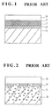
- FIG. 1 illustrates a structure of the SOI substrate.
- a first silicon oxide film 12 having a thickness of 1 micrometer is formed on a silicon supporting substrate 11.
- a gettering sink film 13 is formed on the first silicon oxide film 12.
- the gettering sink film 13 comprises a polysilicon film having a thickness of 500 manometers.
- the gettering sink film 13 acts as a getter for gettering the heavy metal contaminant.
- a second silicon oxide film 14 is formed on the gettering sink film 13.
- the second silicon oxide film 14 has a thickness of 20 manometers which is sufficiently thin for allowing the heavy metals to pass through the second silicon oxide film 14.
- a silicon active layer 15 is formed on the second silicon oxide film 14.
- FIG. 2 illustrates a structure of the SOI substrate.
- An insulating film 23 is partially formed on a silicon supporting substrate 21.
- a silicon active layer 21 is formed on the insulating film 23 so that the silicon active layer 21 is partially in contact with the silicon supporting substrate 21.
- the silicon supporting substrate 21 is subjected to the intrinsic gettering treatment so that the silicon supporting substrate 21 has crystal defects 22.
- the silicon supporting substrate 21 may be prepared as follows.
- a silicon supporting substrate 21 is having an oxygen concentration of 1.5 ⁇ 1018 atoms/cm3 is prepared and then subjected to a heat treatment at about 700°C in nitrogen atmosphere for 10-20 hours, thereby oxygen atoms are extracted from the supporting substrate.
- the crystal defects 22 are formed in the silicon supporting substrate 21.
- the heavy metal contaminant is diffused and moved from the silicon active layer 24 to the silicon supporting substrate 21.
- the crystal defects are used as the gettering.
- the heavy metal is captured by the gettering during the heat treatment.
- the above methods causes a super-saturation state of the heavy metal contaminant in the silicon active layer to thereby cause the extraction of the heavy metal contaminant.
- the heavy metal contaminant is captured by the getter.
- a low temperature below 750°C it is easy to cause the super-saturation state of the heavy metal contaminant.
- a high temperature above 800°C it is difficult to cause the super-saturation state of the heavy metal contaminant.
- the heavy metal contaminant is likely to elute from the getters in the supporting substrate.
- the reduction in the thickness of the insulating film is effective to facilitate the diffusion of the heavy metal contaminant from the silicon active layer to the supporting substrate.
- reduction in the thickness of the insulating film makes it difficult to keep the necessary insulating ability.
- the present invention provides an SOI substrate which comprises a silicon supporting substrate, an insulating film formed on the top of the silicon supporting substrate and a silicon active layer formed on the insulating film.
- the silicon supporting substrate is doped with an impurity at a concentration not less than 1 ⁇ 1017 atoms/cm3, provided that the impurity is kept in the solid solution state at a solidifying point of silicon.
- the impurity may comprise boron, phosphorus and arsenic.
- the silicon active layer has an impurity concentration not less than 1 ⁇ 1015 atoms/cm3, provided that the impurity concentration of the silicon supporting substrate is equal to 100 times or more of the impurity concentration of the silicon active layer.
- the insulating film between the silicon active layer and the silicon supporting substrate has a thickness which satisfy the following relationship. d ⁇ (Dt)/10 , where d is the thickness of the insulating film, t is the time of isothermal treatment of the SOI substrate and D is the diffusion coefficient.
- FIG. 1 is a cross sectional elevation view illustrative of the conventional SOI substrate.
- FIG. 2 is a cross sectional elevation view illustrative of the conventional SOI substrate.
- FIGS. 3A-3C are cross sectional elevation views illustrative of novel SOI substrates in a sequential fabrication process in a first embodiment according to the present invention.
- FIG. 4 is a diagram illustrative of the variation in the density of crystal defects in the active layer versus the boron concentration of the silicon supporting substrate.
- FIG. 5 is a diagram illustrative of the densities of crystal defects in the active layer of the first embodiment and the comparative example.
- FIGS. 6A-6C are cross sectional elevation views illustrative of novel SOI substrates in a sequential fabrication process in a second embodiment according to the present invention.
- FIG. 7 is a diagram illustrative of the densities of crystal defects in the active layer of the second embodiment and the comparative example.
- FIG. 8 is a cross sectional elevation view illustrative of a novel SOI substrate in a third embodiment according to the present invention.
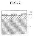
- FIG. 9 is a cross sectional elevation view illustrative of a novel SOI substrate in a third embodiment according to the present invention.
- an SOI substrate comprises a silicon supporting substrate, an insulating film formed on the top of the silicon supporting substrate and a silicon active layer formed on the insulating film.
- the silicon supporting substrate is doped with an impurity at a concentration not less than 1 ⁇ 1017 atoms/cm3, provided that the impurity is kept in the solid solution state at a solidifying point of silicon.
- the impurity may comprise boron, phosphorus and arsenic.
- the silicon active layer has an impurity concentration not less than 1 ⁇ 1015 atoms/cm3, provided that the impurity concentration of the silicon supporting substrate is equal to 100 times or more of the impurity concentration of the silicon active layer.
- the insulating film between the silicon active layer and the silicon supporting substrate has a thickness which satisfy the following relationship. d ⁇ (Dt)/10 , where d is the thickness of the insulating film, t is the time of isothermal treatment of the SOI substrate and D is the diffusion coefficient.
- Tile insulating film may be formed partially on the top of the silicon supporting substrate.
- the present invention utilizes the fact that the impurity doped in the silicon supporting substrate can raise the solid solubility of the heavy metals into the silicon supporting substrate.
- the impurity doped in the silicon supporting substrate can raise the gettering ability.
- the gettering ability depends on both the impurity concentration of the silicon supporting substrate and the temperature of the heat treatment for gettering process. The increase in the temperature of the heat treatment for the gettering process can raise the gettering ability. The increase in the impurity concentration of the supporting substrate can raise the gettering ability.
- the present invention is free from the problems described above. It is preferable to carry out the heat treatment for the gettering at a high temperature so that the diffusion of the heavy metals is encouraged sufficiently for passing through the insulating film.
- a first embodiment according to the present invention will be described, wherein a novel SOI substrate is provided.
- the novel SOI substrate is fabricated as follows. As illustrated in FIG. 3A, a p-type silicon substrate 1 has an impurity concentration of 1 ⁇ 1016 atoms/cm3. The silicon substrate 1 is subjected to a thermal oxidation thereby a silicon oxide film 2 having a thickness of about 0.5 micrometers is formed on the top of the silicon substrate 1.
- a silicon supporting substrate 3 is prepared by doping boron at a concentration of 1 ⁇ 1018 atoms/cm3 and then adhered on the surface of the silicon oxide film 2 by a heat treatment at 1100°C in the nitrogen atmosphere for 2 hours.
- the silicon oxide film 2 is thus sandwiched between the silicon supporting substrate 3 and the silicon substrate 1.
- the silicon substrate 1 is polished to form a silicon active layer 1a having a thickness of about 2 micrometers.
- the silicon active layer 1a is formed on the silicon oxide film 2 which is provided on the silicon supporting substrate 3 highly doped with boron.
- FIG. 4 illustrates the variation in the density of the crystal defects of the silicon supporting substrate 3 versus boron concentration of the silicon active layer 1a, provided that the boron concentration of the silicon active layer 1a is fixed at 1 ⁇ 1015 atoms/cm3.
- the contaminant comprises Cu.
- Cu is applied at a concentration of 1 ⁇ 1014 atoms/cm3 on the surface of the silicon active layer 1a of the SOI substrate.
- the SOI substrate is then subjected to a heat treatment at 900°C in the nitrogen atmosphere for 2 hours.
- the contaminant Cu is likely to be moved into the silicon supporting substrate 3.
- Some of the contaminant Cu remain in the silicon active layer 1a.
- the remaining Cu generates the crystal defects in the silicon active layer 1a.
- a small density of the crystal defects means the fact that a small number of the contaminant Cu atoms remain in the silicon active layer 1a.
- the boron concentration of the silicon supporting substrate 3 is increased from 1 ⁇ 1014 atoms/cm3 to 1 ⁇ 1019 atoms/cm3, the density of the crystal defects of the silicon supporting substrate 3 is reduced.
- the boron concentration of the silicon supporting substrate 3 is increased from 1 ⁇ 1015 atoms/cm3 to 1 ⁇ 1017 atoms/cm3, the density of the crystal defects of the silicon active layer 1a is reduced to about one tenth.
- the boron concentration of the silicon supporting substrate 3 achieves at about 1 ⁇ 1019 atoms/cm3, then the gettering of almost all of the Cu is obtained.
- the increase in the boron concentration of the silicon supporting substrate 3 can raise the amount of Cu in the solid solution state. This relationship is the same when the impurity comprises other atoms such as phosphorus, arsenic and antimony.
- a possible high impurity concentration of the silicon supporting substrate is preferable, but required not to beyond the critical concentration which is the maximum of the amount of impurity in the solid soluble to silicon at a solidifying point of silicon.
- Silicon is metal in the crucible set at 1420°C and then cooled down and solidified at the solidifying point.
- the solid soluble critical concentration of boron is about 6 ⁇ 1020 atoms/cm3.
- the solid soluble critical concentrations of phosphorus and arsenic are about 2 ⁇ 1020 atoms/cm3 and 4 ⁇ 1020 atoms/cm3.
- the heavy metal contaminant is distributed into the silicon active layer 1a and the silicon supporting substrate 3 on the biases of a constant segregation coefficient which depends on an impurity concentration ratio of the silicon active layer 1a to the silicon supporting substrate 1.
- the impurity concentration of the silicon supporting substrate is higher than the impurity concentration of the silicon active layer, then the amount of the heavy metal contaminant to be distributed into the silicon supporting substrate is larger than the amount of the heavy metal contaminant to be distributed into the silicon active layer 1a. Namely, the increase in the impurity concentration of the silicon supporting substrate can arise the gettering ability. It is preferable that the impurity concentration of the silicon supporting substrate is above 100 times of the impurity concentration of the silicon active layer.
- the SOI substrate of the first embodiment was compared to an SOI substrate of the comparative example.
- the silicon supporting substrate has a boron impurity concentration of 1 ⁇ 1016 atoms/cm3.
- the silicon oxide film has a thickness of 0.5 micrometers.
- the getter comprises the crystal defect generated by the oxygen extraction method.
- the SOI substrate is subjected to the Cu contamination.
- the SOI substrate of the present invention as illustrated in FIG. 5 shows a low density of the crystal defects in the silicon active layer 1a.
- the density is 1 ⁇ 102/cm3. This indicates that the gettering ability is high.
- the SOI substrate of the comparative example shows a high density of the crystal defects in the silicon active layer 1a.
- the density is 1 ⁇ 104 /cm3.This indicates that the gettering ability is low.
- MOS diodes are formed on the SOI substrates of the first embodiment and the comparative example respectively to measure minority carrier life times thereof.
- the minority carrier life time is 2200 ⁇ 300 microseconds.
- the minority carrier life time is 700 ⁇ 200 microseconds. This indicates that the SOI substrate of the first embodiment reduces the leakage of current of the device.
- DRAMs are formed on the SOI substrate of the first embodiment, the performance of the memory is superior and the device performance and the yield thereof are considerably improved.
- the contaminant comprises Fe, Ni and Cr.
- the impurity concentration of the silicon supporting substrate 3 is equal to or above 1 ⁇ 1017 atoms/cm3.
- the insulating film has a thickness which satisfy the following relationship. d ⁇ (Dt)/10 , where d is the thickness of the insulating film, t is the time of isothermal treatment of the SOI substrate and D is the diffusion coefficient.
- a second embodiment according to the present invention will be described, wherein a novel SOI substrate is provided.
- the novel SOI substrate is fabricated as follows. As illustrated in FIG. 6A, a p-type silicon substrate 1 has an impurity concentration of 1 ⁇ 1015 atoms/cm3. The silicon substrate 1 is subjected to a thermal oxidation thereby a silicon oxide film 2 having a thickness of about 0.5 micrometers is formed on the top of the silicon substrate 1.
- a silicon supporting substrate 3 is prepared by doping boron at a concentration of 1 ⁇ 1018 atoms/cm3.
- a silicon epitaxial layer 4 having a thickness of about 20 micrometers and a boron impurity concentration of 1 ⁇ 1016 atoms/cm3 is formed on the silicon supporting substrate 3. Thereafter, the silicon epitaxial layer 4 is then adhered on the surface of the silicon oxide film 2 by a heat treatment at 1100°C in the nitrogen atmosphere for 2 hours. The silicon oxide film 2 is thus sandwiched between the silicon supporting substrate 3 and the silicon substrate 1.
- the silicon substrate 1 is polished to form a silicon active layer 1a having a thickness of about 0.1 micrometers.
- the silicon active layer 1a is formed on the silicon oxide film 2 which is provided on the silicon supporting substrate 3 highly doped with boron.
- FIG. 4 illustrates the variation in the density of the crystal defects of the silicon supporting substrate 3 versus boron concentration of the silicon active layer 1a, provided that the boron concentration of the silicon active layer 1a is fixed at 1 ⁇ 1015 atoms/cm3.
- the contaminant comprises Cu.
- Cu is applied at a concentration of 1 ⁇ 1014 atoms/cm3 on the surface of the silicon active layer 1a of the SOI substrate.
- the SOI substrate is then subjected to a heat treatment at 900°C in the nitrogen atmosphere for 2 hours.
- the contaminant Cu is likely to be moved into the silicon supporting substrate 3.
- Some of the contaminant Cu remain in the silicon active layer 1a.
- the remaining Cu generates the crystal defects in the silicon active layer 1a.
- a small density of the crystal defects means the fact that a small number of the contaminant Cu atoms remain in the silicon active layer 1a.
- the boron concentration of the silicon supporting substrate 3 is increased from 1 ⁇ 1014 atoms/cm3 to 1 ⁇ 1019 atoms/cm3, the density of the crystal defects of the silicon supporting substrate 3 is reduced.
- the boron concentration of the silicon supporting substrate 3 is increased from 1 ⁇ 1015 atoms/cm3 to 1 ⁇ 1017 atoms/cm3, the density of the crystal defects of the silicon active layer 1a is reduced to about one tenth.
- the boron concentration of the silicon supporting substrate 3 achieves at about 1 ⁇ 1019 atoms/cm3, then the gettering of almost all of the Cu is obtained.
- the increase in the boron concentration of the silicon supporting substrate 3 can raise the amount of Cu in the solid solution state. This relationship is the same when the impurity comprises other atoms such as phosphorus, arsenic and antimony.
- a possible high impurity concentration of the silicon supporting substrate is preferable, but required not to beyond the critical concentration which is the maximum of the amount of impurity in the solid soluble to silicon at a solidifying point of silicon.
- Silicon is metal in the crucible set at 1420°C and then cooled down and solidified at the solidifying point.
- the solid soluble critical concentration of boron is about 6 ⁇ 1020 atoms/cm3.
- the solid soluble critical concentrations of phosphorus and arsenic are about 2 ⁇ 1020 atoms/cm3 and 4 ⁇ 1020 atoms/cm3.
- the heavy metal contaminant is distributed into the silicon active layer 1a and the silicon supporting substrate 3 on the biases of a constant segregation coefficient which depends on an impurity concentration ratio of the silicon active layer 1a to the silicon supporting substrate 1.
- the impurity concentration of the silicon supporting substrate is higher than the impurity concentration of the silicon active layer, then the amount of the heavy metal contaminant to be distributed into the silicon supporting substrate is larger than the amount of the heavy metal contaminant to be distributed into the silicon active layer 1a. Namely, the increase in the impurity concentration of the silicon supporting substrate can arise the gettering ability. It is preferable that the impurity concentration of the silicon supporting substrate is above 100 times of the impurity concentration of the silicon active layer.
- the SOI substrate of the second embodiment was compared to an SOI substrate of the comparative example.
- the silicon supporting substrate has a boron impurity concentration of 1 ⁇ 1016 atoms/cm3.
- the silicon oxide film has a thickness of 0.5 micrometers.
- the getter comprises the crystal defect generated by the Cu contamination at 1 ⁇ 1013 atoms/cm2 and subsequent heat treatment 1100°C in the nitrogen atmosphere for one hour.
- the SOI substrate of the present invention shows a low density of the crystal defects in the silicon active layer 1a.
- the density is 1 ⁇ 102 /cm3. This indicates that the gettering ability is high.
- the SOI substrate of the comparative example shows a high density of the crystal defects in the silicon active layer 1a.
- the density is above 1 ⁇ 104 /cm3. This indicates that the gettering ability is low.
- MOS diodes are formed on the SOI substrates of the first embodiment and the comparative example respectively to measure minority carrier life times thereof.
- the minority carrier life time is 1500 ⁇ 100 microseconds.
- the minority carrier life time is 500 ⁇ 150 microseconds. This indicates that the SOI substrate of the first embodiment reduces the leakage of current of the device.
- DRAMs are formed on the SOI substrate of the first embodiment, the performance of the memory is superior and the device performance and the yield thereof are considerably improved.
- the contaminant comprises Fe, Ni and Cr.
- the silicon epitaxial layer prevents boron atoms to move from the silicon supporting substrate 3 to the silicon active layer 1a.
- the impurity concentration of the silicon supporting substrate 3 is equal to or above 1 ⁇ 1017 atoms/cm3.
- the insulating film has a thickness which satisfy the following relationship. d ⁇ (Dt)/10 , where d is the thickness of the insulating film, t is the time of isothermal treatment of the SOI substrate and D is the diffusion coefficient.
- a third embodiment according to the present invention will be described, wherein a novel SOI substrate is provided.
- the novel SOI substrate is illustrated in FIG. 8.
- An insulating film 2a having a thickness in the range of 0.1 micrometers to 1.0 micrometer is selectively formed on the top of the silicon supporting substrate 3.
- the silicon supporting substrate is doped with boron at the same concentration as the first embodiment.
- a silicon active layer 1a having a thickness in the range of 10-50 micrometers is provided on the insulating film 2a so that the silicon active layer 1a is partially in contact with the silicon supporting substrate 3. This structure permits the diffusion of the heavy metal contaminant from the active layer 1a via the gaps of the silicon oxide film 2a to the silicon supporting substrate 3.
- a fourth embodiment according to the present invention will be described, wherein a novel SOI substrate is provided.
- the novel SOI substrate is illustrated in FIG. 9.
- a silicon epitaxial layer 4 is formed on the silicon supporting substrate 3.
- the silicon supporting substrate 3 is doped with boron at the same concentration as the first embodiment.
- An insulating film 2a having a thickness in the range of 0.1 micrometers to 1.0 micrometer is selectively formed on the top of the silicon epitaxial layer 4.
- a silicon active layer 1a having a thickness in the range of 10-50 micrometers is provided on the insulating film 2a so that the silicon active layer 1a is partially in contact with the silicon epitaxial layer 4.
- Partially providing the silicon oxide film permits the diffusion of the heavy metal contaminant from the active layer 1a via the gaps of the silicon oxide film 2a to the silicon supporting substrate 3.
- the silicon epitaxial layer 4 prevents the heavy metal contaminant to be diffused from the silicon supporting substrate 3 to the silicon active layer 1a.
Abstract
Description
- The present invention relates to a silicon-on-insulator (SOI) substrate, which shows an improved feature for gettering heavy metals as contaminant.
- The silicon-on-insulator (SOI) substrate is useful to suppress problems of a latch-up phenomenon and a short channel effect which appear when the scaling down of the semiconductor device is progressed. The silicon-on-insulator (SOI) substrate is also attractive as allowing a high speed performance of the device at a low driving voltage.
- The progress of the scaling down of the device and the raising in the density of the integration of the semiconductor circuits can arise another problem of the contamination of a semiconductor active region by heavy metals such as Fe, Cu, Cr and Ni. The contamination is caused during the fabrication process. The contamination of the semiconductor active region can cause a reduction in the yield of the device, a deterioration of the device performances and a lowering of the reliability. Under these circumstances, the importance of the removal of the heavy metal contaminant from the semiconductor active region is now on the increase.
- For the silicon substrate other than the SOI substrate, the following methods may be effective to remove the heavy metal contaminant. An intrinsic gettering method uses, as getters, crystal defects or extraction generated by extracting oxygen from the silicon substrate. A back side gettering method uses, as getters, crystal defects generated by mechanical damages. A polysilicon gettering method uses a polysilicon layer as a getter. A phosphorus doping gettering method uses a diffusion layer highly doped with phosphorus as a getter. The getter is formed at the interior or the bottom of the silicon substrate. The heavy metal contaminant is captured by the getter during heat treatments in the fabrication processes of the device.
- In the SOI substrate, the silicon active layer is separated by an insulating layer from a supporting substrate in which the heavy metal getter is formed. The insulating layer can prevent a diffusion of the heavy metal contaminant from the active region into the supporting substrate.
- To settle this problem, some improvements have been made. One improvement is disclosed in the Japanese laid-open patent application No. 4-199632. FIG. 1 illustrates a structure of the SOI substrate. A first
silicon oxide film 12 having a thickness of 1 micrometer is formed on asilicon supporting substrate 11. A getteringsink film 13 is formed on the firstsilicon oxide film 12. The getteringsink film 13 comprises a polysilicon film having a thickness of 500 manometers. The getteringsink film 13 acts as a getter for gettering the heavy metal contaminant. A secondsilicon oxide film 14 is formed on the getteringsink film 13. The secondsilicon oxide film 14 has a thickness of 20 manometers which is sufficiently thin for allowing the heavy metals to pass through the secondsilicon oxide film 14. A siliconactive layer 15 is formed on the secondsilicon oxide film 14. - Another improvement I disclosed in the Japanese laid-open patent application No. 2-237121. FIG. 2 illustrates a structure of the SOI substrate. An
insulating film 23 is partially formed on asilicon supporting substrate 21. A siliconactive layer 21 is formed on theinsulating film 23 so that the siliconactive layer 21 is partially in contact with thesilicon supporting substrate 21. Thesilicon supporting substrate 21 is subjected to the intrinsic gettering treatment so that thesilicon supporting substrate 21 hascrystal defects 22. Thesilicon supporting substrate 21 may be prepared as follows. Asilicon supporting substrate 21 is having an oxygen concentration of 1.5 × 10¹⁸ atoms/cm³ is prepared and then subjected to a heat treatment at about 700°C in nitrogen atmosphere for 10-20 hours, thereby oxygen atoms are extracted from the supporting substrate. As a result, thecrystal defects 22 are formed in thesilicon supporting substrate 21. The heavy metal contaminant is diffused and moved from the siliconactive layer 24 to thesilicon supporting substrate 21. - In the prior art described above, the crystal defects are used as the gettering. The heavy metal is captured by the gettering during the heat treatment. The above methods causes a super-saturation state of the heavy metal contaminant in the silicon active layer to thereby cause the extraction of the heavy metal contaminant. As a result of the extraction, the heavy metal contaminant is captured by the getter. At a low temperature below 750°C, it is easy to cause the super-saturation state of the heavy metal contaminant. At a high temperature above 800°C, it is difficult to cause the super-saturation state of the heavy metal contaminant. At the low temperature below 750°C, a thermal diffusion of the heavy metal contaminant from the silicon active layer to the silicon supporting substrate is likely to be prevented by the insulating film. At the high temperature above 800°C, it is hard to cause the super-saturation state of the heavy metal contaminant which is necessary for causing the gettering. Once the substrate is subjected to the heat treatment at a higher temperature than the optimum temperature for the gettering, the heavy metal contaminant is likely to elute from the getters in the supporting substrate.
- Indeed, the reduction in the thickness of the insulating film is effective to facilitate the diffusion of the heavy metal contaminant from the silicon active layer to the supporting substrate. However, reduction in the thickness of the insulating film makes it difficult to keep the necessary insulating ability.
- It has been required to develop a novel SOI substrate which has a sufficient gettering ability.
- Accordingly, it is an object of the present invention to provide a novel SOI substrate, which is free from the above problems.
- The above and other objects, features and advantages of the present invention will be apparent from the following descriptions.
- The present invention provides an SOI substrate which comprises a silicon supporting substrate, an insulating film formed on the top of the silicon supporting substrate and a silicon active layer formed on the insulating film. The silicon supporting substrate is doped with an impurity at a concentration not less than 1 × 10¹⁷ atoms/cm³, provided that the impurity is kept in the solid solution state at a solidifying point of silicon. The impurity may comprise boron, phosphorus and arsenic.
- The silicon active layer has an impurity concentration not less than 1 × 10¹⁵ atoms/cm³, provided that the impurity concentration of the silicon supporting substrate is equal to 100 times or more of the impurity concentration of the silicon active layer.
- It is available to provide a mono-crystal silicon layer between the insulating film and the silicon supporting substrate, wherein the mono-crystal silicon layer has an impurity concentration lower than the impurity concentration of the silicon supporting substrate.
- The insulating film between the silicon active layer and the silicon supporting substrate has a thickness which satisfy the following relationship.

- Preferred embodiments of the present invention will be described in detail with reference to the accompanying drawings.
- FIG. 1 is a cross sectional elevation view illustrative of the conventional SOI substrate.
- FIG. 2 is a cross sectional elevation view illustrative of the conventional SOI substrate.
- FIGS. 3A-3C are cross sectional elevation views illustrative of novel SOI substrates in a sequential fabrication process in a first embodiment according to the present invention.
- FIG. 4 is a diagram illustrative of the variation in the density of crystal defects in the active layer versus the boron concentration of the silicon supporting substrate.
- FIG. 5 is a diagram illustrative of the densities of crystal defects in the active layer of the first embodiment and the comparative example.
- FIGS. 6A-6C are cross sectional elevation views illustrative of novel SOI substrates in a sequential fabrication process in a second embodiment according to the present invention.
- FIG. 7 is a diagram illustrative of the densities of crystal defects in the active layer of the second embodiment and the comparative example.
- FIG. 8 is a cross sectional elevation view illustrative of a novel SOI substrate in a third embodiment according to the present invention.
- FIG. 9 is a cross sectional elevation view illustrative of a novel SOI substrate in a third embodiment according to the present invention.
- According to the present invention, an SOI substrate comprises a silicon supporting substrate, an insulating film formed on the top of the silicon supporting substrate and a silicon active layer formed on the insulating film. The silicon supporting substrate is doped with an impurity at a concentration not less than 1 × 10¹⁷ atoms/cm³, provided that the impurity is kept in the solid solution state at a solidifying point of silicon. The impurity may comprise boron, phosphorus and arsenic.
- The silicon active layer has an impurity concentration not less than 1 × 10¹⁵ atoms/cm³, provided that the impurity concentration of the silicon supporting substrate is equal to 100 times or more of the impurity concentration of the silicon active layer.
- It is available to provide a mono-crystal silicon layer between the insulating film and the silicon supporting substrate, wherein the mono-crystal silicon layer has an impurity concentration lower than the impurity concentration of the silicon supporting substrate.
- The insulating film between the silicon active layer and the silicon supporting substrate has a thickness which satisfy the following relationship.

- Tile insulating film may be formed partially on the top of the silicon supporting substrate.
- According to the present invention, no extraction of oxygen nor crystal defect is utilized. The present invention utilizes the fact that the impurity doped in the silicon supporting substrate can raise the solid solubility of the heavy metals into the silicon supporting substrate. Namely, the impurity doped in the silicon supporting substrate can raise the gettering ability. The gettering ability depends on both the impurity concentration of the silicon supporting substrate and the temperature of the heat treatment for gettering process. The increase in the temperature of the heat treatment for the gettering process can raise the gettering ability. The increase in the impurity concentration of the supporting substrate can raise the gettering ability. For the present invention, it is not necessary to cause the super-saturation state of the heavy metal contaminant. Even if the SOI substrate is subjected to a high temperature heat treatment, the heavy meats do not elute to the silicon active layer from the getters in the supporting substrate. For those reasons, the present invention is free from the problems described above. It is preferable to carry out the heat treatment for the gettering at a high temperature so that the diffusion of the heavy metals is encouraged sufficiently for passing through the insulating film.
- A first embodiment according to the present invention will be described, wherein a novel SOI substrate is provided. The novel SOI substrate is fabricated as follows. As illustrated in FIG. 3A, a p-
type silicon substrate 1 has an impurity concentration of 1 × 10¹⁶ atoms/cm³. Thesilicon substrate 1 is subjected to a thermal oxidation thereby asilicon oxide film 2 having a thickness of about 0.5 micrometers is formed on the top of thesilicon substrate 1. - As illustrated in FIG. 3B, a
silicon supporting substrate 3 is prepared by doping boron at a concentration of 1 × 10¹⁸ atoms/cm³ and then adhered on the surface of thesilicon oxide film 2 by a heat treatment at 1100°C in the nitrogen atmosphere for 2 hours. Thesilicon oxide film 2 is thus sandwiched between thesilicon supporting substrate 3 and thesilicon substrate 1. - As illustrated in FIG. 3C, the
silicon substrate 1 is polished to form a silicon active layer 1a having a thickness of about 2 micrometers. As a result, the silicon active layer 1a is formed on thesilicon oxide film 2 which is provided on thesilicon supporting substrate 3 highly doped with boron. - As a modification, it is available to dope n-type impurity into the
silicon supporting substrate 3 at 1 × 10¹⁴ atoms/cm³. - The gettering ability of the novel SOI substrate was measured. FIG. 4 illustrates the variation in the density of the crystal defects of the
silicon supporting substrate 3 versus boron concentration of the silicon active layer 1a, provided that the boron concentration of the silicon active layer 1a is fixed at 1 × 10¹⁵ atoms/cm³. The contaminant comprises Cu. Cu is applied at a concentration of 1 × 10¹⁴ atoms/cm³ on the surface of the silicon active layer 1a of the SOI substrate. The SOI substrate is then subjected to a heat treatment at 900°C in the nitrogen atmosphere for 2 hours. The contaminant Cu is likely to be moved into thesilicon supporting substrate 3. Some of the contaminant Cu remain in the silicon active layer 1a. The remaining Cu generates the crystal defects in the silicon active layer 1a. A small density of the crystal defects means the fact that a small number of the contaminant Cu atoms remain in the silicon active layer 1a. - As the boron concentration of the
silicon supporting substrate 3 is increased from 1 × 10¹⁴ atoms/cm³ to 1 × 10¹⁹ atoms/cm³, the density of the crystal defects of thesilicon supporting substrate 3 is reduced. As the boron concentration of thesilicon supporting substrate 3 is increased from 1 × 10¹⁵ atoms/cm³ to 1 × 10¹⁷ atoms/cm³, the density of the crystal defects of the silicon active layer 1a is reduced to about one tenth. As the boron concentration of thesilicon supporting substrate 3 achieves at about 1 × 10¹⁹ atoms/cm³, then the gettering of almost all of the Cu is obtained. The increase in the boron concentration of thesilicon supporting substrate 3 can raise the amount of Cu in the solid solution state. This relationship is the same when the impurity comprises other atoms such as phosphorus, arsenic and antimony. - A possible high impurity concentration of the silicon supporting substrate is preferable, but required not to beyond the critical concentration which is the maximum of the amount of impurity in the solid soluble to silicon at a solidifying point of silicon. Silicon is metal in the crucible set at 1420°C and then cooled down and solidified at the solidifying point. The solid soluble critical concentration of boron is about 6 × 10²⁰ atoms/cm³. The solid soluble critical concentrations of phosphorus and arsenic are about 2 × 10²⁰ atoms/cm³ and 4 × 10²⁰ atoms/cm³.
- The heavy metal contaminant is distributed into the silicon active layer 1a and the
silicon supporting substrate 3 on the biases of a constant segregation coefficient which depends on an impurity concentration ratio of the silicon active layer 1a to thesilicon supporting substrate 1. When the impurity concentration of the silicon supporting substrate is higher than the impurity concentration of the silicon active layer, then the amount of the heavy metal contaminant to be distributed into the silicon supporting substrate is larger than the amount of the heavy metal contaminant to be distributed into the silicon active layer 1a. Namely, the increase in the impurity concentration of the silicon supporting substrate can arise the gettering ability. It is preferable that the impurity concentration of the silicon supporting substrate is above 100 times of the impurity concentration of the silicon active layer. - The SOI substrate of the first embodiment was compared to an SOI substrate of the comparative example. In the comparative example, the silicon supporting substrate has a boron impurity concentration of 1 × 10¹⁶ atoms/cm³. The silicon oxide film has a thickness of 0.5 micrometers. The getter comprises the crystal defect generated by the oxygen extraction method. The SOI substrate is subjected to the Cu contamination.
- The SOI substrate of the present invention as illustrated in FIG. 5 shows a low density of the crystal defects in the silicon active layer 1a. The density is 1 × 10²/cm³. This indicates that the gettering ability is high. By contrast, the SOI substrate of the comparative example shows a high density of the crystal defects in the silicon active layer 1a. The density is 1 × 10⁴ /cm³.This indicates that the gettering ability is low.
- MOS diodes are formed on the SOI substrates of the first embodiment and the comparative example respectively to measure minority carrier life times thereof. In the first embodiment, the minority carrier life time is 2200±300 microseconds. In the comparative example, the minority carrier life time is 700±200 microseconds. This indicates that the SOI substrate of the first embodiment reduces the leakage of current of the device. When DRAMs are formed on the SOI substrate of the first embodiment, the performance of the memory is superior and the device performance and the yield thereof are considerably improved.
- The above remarkable effects of the present invention could be confirmed when the contaminant comprises Fe, Ni and Cr.
- The following was also confirmed. It is effective to reduce the contaminant concentration to one tenth. It is preferable that the impurity concentration of the
silicon supporting substrate 3 is equal to or above 1 × 10¹⁷ atoms/cm³. - It is preferable for obtaining the sufficiently high gettering ability that the insulating film has a thickness which satisfy the following relationship.

- A second embodiment according to the present invention will be described, wherein a novel SOI substrate is provided. The novel SOI substrate is fabricated as follows. As illustrated in FIG. 6A, a p-
type silicon substrate 1 has an impurity concentration of 1 × 10¹⁵ atoms/cm³. Thesilicon substrate 1 is subjected to a thermal oxidation thereby asilicon oxide film 2 having a thickness of about 0.5 micrometers is formed on the top of thesilicon substrate 1. - As illustrated in FIG. 6B, a
silicon supporting substrate 3 is prepared by doping boron at a concentration of 1 × 10¹⁸ atoms/cm³. Asilicon epitaxial layer 4 having a thickness of about 20 micrometers and a boron impurity concentration of 1 × 10¹⁶ atoms/cm³ is formed on thesilicon supporting substrate 3. Thereafter, thesilicon epitaxial layer 4 is then adhered on the surface of thesilicon oxide film 2 by a heat treatment at 1100°C in the nitrogen atmosphere for 2 hours. Thesilicon oxide film 2 is thus sandwiched between thesilicon supporting substrate 3 and thesilicon substrate 1. - As illustrated in FIG. 6C, the
silicon substrate 1 is polished to form a silicon active layer 1a having a thickness of about 0.1 micrometers. As a result, the silicon active layer 1a is formed on thesilicon oxide film 2 which is provided on thesilicon supporting substrate 3 highly doped with boron. - As a modification, it is available to dope n-type impurity into the
silicon supporting substrate 3 at 1 × 10¹⁴ atoms/cm³. - The gettering ability of the novel SOI substrate was measured. FIG. 4 illustrates the variation in the density of the crystal defects of the
silicon supporting substrate 3 versus boron concentration of the silicon active layer 1a, provided that the boron concentration of the silicon active layer 1a is fixed at 1 × 10¹⁵ atoms/cm³. The contaminant comprises Cu. Cu is applied at a concentration of 1 × 10¹⁴ atoms/cm³ on the surface of the silicon active layer 1a of the SOI substrate. The SOI substrate is then subjected to a heat treatment at 900°C in the nitrogen atmosphere for 2 hours. The contaminant Cu is likely to be moved into thesilicon supporting substrate 3. Some of the contaminant Cu remain in the silicon active layer 1a. The remaining Cu generates the crystal defects in the silicon active layer 1a. A small density of the crystal defects means the fact that a small number of the contaminant Cu atoms remain in the silicon active layer 1a. - As the boron concentration of the
silicon supporting substrate 3 is increased from 1 × 10¹⁴ atoms/cm³ to 1 × 10¹⁹ atoms/cm³, the density of the crystal defects of thesilicon supporting substrate 3 is reduced. As the boron concentration of thesilicon supporting substrate 3 is increased from 1 × 10¹⁵ atoms/cm³ to 1 × 10¹⁷ atoms/cm³, the density of the crystal defects of the silicon active layer 1a is reduced to about one tenth. As the boron concentration of thesilicon supporting substrate 3 achieves at about 1 × 10¹⁹ atoms/cm³, then the gettering of almost all of the Cu is obtained. The increase in the boron concentration of thesilicon supporting substrate 3 can raise the amount of Cu in the solid solution state. This relationship is the same when the impurity comprises other atoms such as phosphorus, arsenic and antimony. - A possible high impurity concentration of the silicon supporting substrate is preferable, but required not to beyond the critical concentration which is the maximum of the amount of impurity in the solid soluble to silicon at a solidifying point of silicon. Silicon is metal in the crucible set at 1420°C and then cooled down and solidified at the solidifying point. The solid soluble critical concentration of boron is about 6 × 10²⁰ atoms/cm³. The solid soluble critical concentrations of phosphorus and arsenic are about 2 × 10²⁰ atoms/cm³ and 4 × 10²⁰ atoms/cm³.
- The heavy metal contaminant is distributed into the silicon active layer 1a and the
silicon supporting substrate 3 on the biases of a constant segregation coefficient which depends on an impurity concentration ratio of the silicon active layer 1a to thesilicon supporting substrate 1. When the impurity concentration of the silicon supporting substrate is higher than the impurity concentration of the silicon active layer, then the amount of the heavy metal contaminant to be distributed into the silicon supporting substrate is larger than the amount of the heavy metal contaminant to be distributed into the silicon active layer 1a. Namely, the increase in the impurity concentration of the silicon supporting substrate can arise the gettering ability. It is preferable that the impurity concentration of the silicon supporting substrate is above 100 times of the impurity concentration of the silicon active layer. - The SOI substrate of the second embodiment was compared to an SOI substrate of the comparative example. In the comparative example, the silicon supporting substrate has a boron impurity concentration of 1 × 10¹⁶ atoms/cm³. The silicon oxide film has a thickness of 0.5 micrometers. The getter comprises the crystal defect generated by the Cu contamination at 1 × 10¹³ atoms/cm² and subsequent heat treatment 1100°C in the nitrogen atmosphere for one hour.
- As illustrated in FIG. 7, the SOI substrate of the present invention shows a low density of the crystal defects in the silicon active layer 1a. The density is 1 × 10² /cm³. This indicates that the gettering ability is high. By contrast, the SOI substrate of the comparative example shows a high density of the crystal defects in the silicon active layer 1a. The density is above 1 × 10⁴ /cm³. This indicates that the gettering ability is low.
- MOS diodes are formed on the SOI substrates of the first embodiment and the comparative example respectively to measure minority carrier life times thereof. In the first embodiment, the minority carrier life time is 1500±100 microseconds. In the comparative example, the minority carrier life time is 500±150 microseconds. This indicates that the SOI substrate of the first embodiment reduces the leakage of current of the device. When DRAMs are formed on the SOI substrate of the first embodiment, the performance of the memory is superior and the device performance and the yield thereof are considerably improved.
- The above remarkable effects of the present invention could be confirmed when the contaminant comprises Fe, Ni and Cr.
- The silicon epitaxial layer prevents boron atoms to move from the
silicon supporting substrate 3 to the silicon active layer 1a. - The following was also confirmed. It is effective to reduce the contaminant concentration to one tenth. It is preferable that the impurity concentration of the
silicon supporting substrate 3 is equal to or above 1 × 10¹⁷ atoms/cm³. - It is preferable for obtaining the sufficiently high gettering ability that the insulating film has a thickness which satisfy the following relationship.

- A third embodiment according to the present invention will be described, wherein a novel SOI substrate is provided. The novel SOI substrate is illustrated in FIG. 8. An insulating
film 2a having a thickness in the range of 0.1 micrometers to 1.0 micrometer is selectively formed on the top of thesilicon supporting substrate 3. The silicon supporting substrate is doped with boron at the same concentration as the first embodiment. A silicon active layer 1a having a thickness in the range of 10-50 micrometers is provided on the insulatingfilm 2a so that the silicon active layer 1a is partially in contact with thesilicon supporting substrate 3. This structure permits the diffusion of the heavy metal contaminant from the active layer 1a via the gaps of thesilicon oxide film 2a to thesilicon supporting substrate 3. - A fourth embodiment according to the present invention will be described, wherein a novel SOI substrate is provided. The novel SOI substrate is illustrated in FIG. 9. A
silicon epitaxial layer 4 is formed on thesilicon supporting substrate 3. Thesilicon supporting substrate 3 is doped with boron at the same concentration as the first embodiment. An insulatingfilm 2a having a thickness in the range of 0.1 micrometers to 1.0 micrometer is selectively formed on the top of thesilicon epitaxial layer 4. A silicon active layer 1a having a thickness in the range of 10-50 micrometers is provided on the insulatingfilm 2a so that the silicon active layer 1a is partially in contact with thesilicon epitaxial layer 4. Partially providing the silicon oxide film permits the diffusion of the heavy metal contaminant from the active layer 1a via the gaps of thesilicon oxide film 2a to thesilicon supporting substrate 3. Thesilicon epitaxial layer 4 prevents the heavy metal contaminant to be diffused from thesilicon supporting substrate 3 to the silicon active layer 1a. - Whereas modifications of the present invention will be apparent to a person having ordinary skill in the art, to which the invention pertains, it is to be understood that the embodiments described by way of illustrations are by no means intended to be considered in a limiting sense. Accordingly, it is to be intended to cover by claims all modifications of the present invention which fall within the sprite and scope of the present invention.
Claims (8)
- A silicon-on-insulating substrate comprising :
a silicon supporting substrate ;
an insulating film formed on the top of the silicon supporting substrate ; and
a silicon active layer formed on the insulating film, characterized in that the silicon supporting substrate is doped with an impurity at a concentration not less than 1 × 10¹⁷ atoms/cm³, provided that the impurity is kept in the solid solution state at a solidifying point of silicon. - The silicon-on-insulating substrate as claimed in claim 1, characterized in that the impurity comprises boron.
- The silicon-on-insulating substrate as claimed in claim 1, characterized in that the impurity comprises phosphorus.
- The silicon-on-insulating substrate as claimed in claim 1, characterized in that the impurity comprises arsenic.
- The silicon-on-insulating substrate as claimed in claim 1, characterized in that the silicon active layer has an impurity concentration not less than 1 × 10¹⁵ atoms/cm³, provided that the impurity concentration of the silicon supporting substrate is equal to 100 times or more of the impurity concentration of the silicon active layer.
- The silicon-on-insulating substrate as claimed in claim 1, characterized in that the insulating film has a thickness which satisfy the relationship:

- The silicon-on-insulating substrate as claimed in claim 1, characterized in that the insulating film is selectively formed so that the silicon active layer is partially in contact with the silicon supporting substrate.
- The silicon-on-insulating substrate as claimed in claim 1, further comprising a silicon epitaxial layer, having an impurity concentration lower than the impurity concentration of the silicon supporting substrate, between the insulating film and the silicon supporting substrate.
Applications Claiming Priority (2)
| Application Number | Priority Date | Filing Date | Title |
|---|---|---|---|
| JP6272088A JP2755185B2 (en) | 1994-11-07 | 1994-11-07 | SOI substrate |
| JP272088/94 | 1994-11-07 |
Publications (2)
| Publication Number | Publication Date |
|---|---|
| EP0710980A2 true EP0710980A2 (en) | 1996-05-08 |
| EP0710980A3 EP0710980A3 (en) | 1998-09-30 |
Family
ID=17508922
Family Applications (1)
| Application Number | Title | Priority Date | Filing Date |
|---|---|---|---|
| EP95117533A Withdrawn EP0710980A3 (en) | 1994-11-07 | 1995-11-07 | Soi substrate |
Country Status (3)
| Country | Link |
|---|---|
| US (1) | US5753353A (en) |
| EP (1) | EP0710980A3 (en) |
| JP (1) | JP2755185B2 (en) |
Cited By (2)
| Publication number | Priority date | Publication date | Assignee | Title |
|---|---|---|---|---|
| EP1667218A1 (en) * | 2003-09-08 | 2006-06-07 | Sumitomo Mitsubishi Silicon Corporation | Soi wafer and its manufacturing method |
| US7291538B2 (en) | 2001-09-26 | 2007-11-06 | Renesas Technology Corp. | Semiconductor memory device and manufacturing method of the same |
Families Citing this family (7)
| Publication number | Priority date | Publication date | Assignee | Title |
|---|---|---|---|---|
| WO2000010195A2 (en) * | 1998-08-10 | 2000-02-24 | Memc Electronic Materials, Inc. | Preparation of metal-precipitates permeable insulator for soi substrate |
| JP2000323484A (en) | 1999-05-07 | 2000-11-24 | Mitsubishi Electric Corp | Semiconductor device and semiconductor memory |
| JP2000353797A (en) | 1999-06-11 | 2000-12-19 | Mitsubishi Electric Corp | Semiconductor wafer and manufacture thereof |
| US6596570B2 (en) | 2001-06-06 | 2003-07-22 | International Business Machines Corporation | SOI device with reduced junction capacitance |
| JP4534412B2 (en) * | 2002-06-26 | 2010-09-01 | 株式会社ニコン | Solid-state imaging device |
| JP2007134616A (en) * | 2005-11-14 | 2007-05-31 | Nec Electronics Corp | Soi substrate, and method of manufacturing same |
| JP7334698B2 (en) * | 2020-09-11 | 2023-08-29 | 信越半導体株式会社 | SOI WAFER MANUFACTURING METHOD AND SOI WAFER |
Citations (7)
| Publication number | Priority date | Publication date | Assignee | Title |
|---|---|---|---|---|
| EP0335741A2 (en) * | 1988-03-31 | 1989-10-04 | Kabushiki Kaisha Toshiba | Dielectrically isolated semiconductor substrate |
| JPH02237121A (en) * | 1989-03-10 | 1990-09-19 | Fujitsu Ltd | Manufacture of semiconductor device |
| JPH04199632A (en) * | 1990-11-29 | 1992-07-20 | Fujitsu Ltd | Soi wafer and manufacture thereof |
| JPH05129309A (en) * | 1991-10-31 | 1993-05-25 | Nec Corp | Pasted substrate |
| US5298449A (en) * | 1992-03-06 | 1994-03-29 | Nec Corporation | Semiconductor substrate having a silicon-on-insulator structure and method of fabricating the same |
| JPH06163862A (en) * | 1992-11-27 | 1994-06-10 | Nec Corp | Soi substrate structure and its manufacture |
| EP0697713A1 (en) * | 1994-07-21 | 1996-02-21 | Kabushiki Kaisha Toshiba | Silicon on insulator substrate and method of manufacturing the same |
Family Cites Families (13)
| Publication number | Priority date | Publication date | Assignee | Title |
|---|---|---|---|---|
| US4558507A (en) * | 1982-11-12 | 1985-12-17 | Nec Corporation | Method of manufacturing semiconductor device |
| US4591654A (en) * | 1983-07-18 | 1986-05-27 | Nippon Telegraph And Telephone Public Corporation | Solar cells based on indium phosphide |
| JPS60201666A (en) * | 1984-03-27 | 1985-10-12 | Nec Corp | Semiconductor device |
| JPH0628296B2 (en) * | 1985-10-17 | 1994-04-13 | 日本電気株式会社 | Method for manufacturing semiconductor device |
| JP2896141B2 (en) * | 1987-02-26 | 1999-05-31 | 株式会社東芝 | High voltage semiconductor device |
| JPH0795568B2 (en) * | 1987-04-27 | 1995-10-11 | 日本電気株式会社 | Semiconductor memory device |
| JP2762462B2 (en) * | 1988-05-31 | 1998-06-04 | ソニー株式会社 | Semiconductor substrate manufacturing method |
| JPH0691263B2 (en) * | 1988-10-19 | 1994-11-14 | 株式会社東芝 | Method for manufacturing semiconductor device |
| JP2811798B2 (en) * | 1989-09-07 | 1998-10-15 | ソニー株式会社 | Semiconductor substrate manufacturing method |
| US5374846A (en) * | 1990-08-31 | 1994-12-20 | Nec Corporation | Bipolar transistor with a particular base and collector regions |
| US5293512A (en) * | 1991-02-13 | 1994-03-08 | Nec Corporation | Semiconductor device having a groove type isolation region |
| US5229305A (en) * | 1992-02-03 | 1993-07-20 | Motorola, Inc. | Method for making intrinsic gettering sites in bonded substrates |
| JP3295171B2 (en) * | 1993-04-07 | 2002-06-24 | 新日本製鐵株式会社 | Semiconductor substrate manufacturing method |
-
1994
- 1994-11-07 JP JP6272088A patent/JP2755185B2/en not_active Expired - Fee Related
-
1995
- 1995-11-07 US US08/554,720 patent/US5753353A/en not_active Expired - Fee Related
- 1995-11-07 EP EP95117533A patent/EP0710980A3/en not_active Withdrawn
Patent Citations (7)
| Publication number | Priority date | Publication date | Assignee | Title |
|---|---|---|---|---|
| EP0335741A2 (en) * | 1988-03-31 | 1989-10-04 | Kabushiki Kaisha Toshiba | Dielectrically isolated semiconductor substrate |
| JPH02237121A (en) * | 1989-03-10 | 1990-09-19 | Fujitsu Ltd | Manufacture of semiconductor device |
| JPH04199632A (en) * | 1990-11-29 | 1992-07-20 | Fujitsu Ltd | Soi wafer and manufacture thereof |
| JPH05129309A (en) * | 1991-10-31 | 1993-05-25 | Nec Corp | Pasted substrate |
| US5298449A (en) * | 1992-03-06 | 1994-03-29 | Nec Corporation | Semiconductor substrate having a silicon-on-insulator structure and method of fabricating the same |
| JPH06163862A (en) * | 1992-11-27 | 1994-06-10 | Nec Corp | Soi substrate structure and its manufacture |
| EP0697713A1 (en) * | 1994-07-21 | 1996-02-21 | Kabushiki Kaisha Toshiba | Silicon on insulator substrate and method of manufacturing the same |
Non-Patent Citations (7)
| Title |
|---|
| PATENT ABSTRACTS OF JAPAN vol. 014, no. 553 (E-1010), 7 December 1990 -& JP 02 237121 A (FUJITSU LTD), 19 September 1990 * |
| PATENT ABSTRACTS OF JAPAN vol. 016, no. 530 (E-1287), 30 October 1992 -& JP 04 199632 A (FUJITSU LTD), 20 July 1992 * |
| PATENT ABSTRACTS OF JAPAN vol. 017, no. 501 (E-1429), 9 September 1993 -& JP 05 129309 A (NEC CORP), 25 May 1993 * |
| PATENT ABSTRACTS OF JAPAN vol. 018, no. 480 (E-1603), 8 September 1994 -& JP 06 163862 A (NEC CORP), 10 June 1994 * |
| SUNDARESAN R ET AL: "Characterization of leakage current in buried-oxide SOI transistors" IEEE TRANSACTIONS ON ELECTRON DEVICES, SEPT. 1989, USA, vol. 36, no. 9, pt.1, pages 1740-1745, XP002072982 ISSN 0018-9383 * |
| SVEINBJORNSSON E.O. ET AL: 'Phosphorus diffusion gettering of gold in silicon-the reversibility of the gettering process' JOURNAL OF APPLIED PHYSICS, vol. 73, no. 11, 01 June 1993, USA, pages 7311 - 7321 * |
| SZE S.M.: "VLSI Technology, Second Edition", 1988, MCGRAW-HILL, SG,SINGAPORE * |
Cited By (4)
| Publication number | Priority date | Publication date | Assignee | Title |
|---|---|---|---|---|
| US7291538B2 (en) | 2001-09-26 | 2007-11-06 | Renesas Technology Corp. | Semiconductor memory device and manufacturing method of the same |
| US7498207B2 (en) | 2001-09-26 | 2009-03-03 | Renesas Technology Corp. | Semiconductor memory device and manufacturing method of the same |
| EP1667218A1 (en) * | 2003-09-08 | 2006-06-07 | Sumitomo Mitsubishi Silicon Corporation | Soi wafer and its manufacturing method |
| EP1667218A4 (en) * | 2003-09-08 | 2010-11-03 | Sumco Corp | Soi wafer and its manufacturing method |
Also Published As
| Publication number | Publication date |
|---|---|
| JPH08139295A (en) | 1996-05-31 |
| JP2755185B2 (en) | 1998-05-20 |
| EP0710980A3 (en) | 1998-09-30 |
| US5753353A (en) | 1998-05-19 |
Similar Documents
| Publication | Publication Date | Title |
|---|---|---|
| US5413679A (en) | Method of producing a silicon membrane using a silicon alloy etch stop layer | |
| US5414276A (en) | Transistors using crystalline silicon devices on glass | |
| JP2575545B2 (en) | Method for manufacturing semiconductor device | |
| US4548654A (en) | Surface denuding of silicon wafer | |
| US6376336B1 (en) | Frontside SOI gettering with phosphorus doping | |
| US5298449A (en) | Semiconductor substrate having a silicon-on-insulator structure and method of fabricating the same | |
| JPH08116038A (en) | Semiconductor device and its manufacture | |
| CN102239548B (en) | Semiconductor device structures including transistors with energy barriers adjacent to transistor channels and associated methods | |
| EP0710980A2 (en) | Soi substrate | |
| US6114223A (en) | Gettering regions and methods of forming gettering regions within a semiconductor wafer | |
| JP3033655B2 (en) | Semiconductor device and method of manufacturing semiconductor device | |
| KR100288815B1 (en) | Manufacturing Method of Semiconductor Substrate | |
| US5985728A (en) | Silicon on insulator process with recovery of a device layer from an etch stop layer | |
| EP0449589A1 (en) | Method of producing a SOI structure | |
| US6670259B1 (en) | Inert atom implantation method for SOI gettering | |
| WO2007132266A1 (en) | Improvements in semiconductor processing | |
| JP2010040931A (en) | Manufacturing method of semiconductor substrate, and semiconductor substrate | |
| JPH10313011A (en) | Semiconductor substrate formation thereof | |
| JP3579069B2 (en) | Method for manufacturing semiconductor device | |
| JP3452122B2 (en) | Method for manufacturing SOI substrate | |
| JPH11307471A (en) | Manufacture for soi substrate | |
| JP4272607B2 (en) | SOI by oxidation of porous silicon | |
| JP3296307B2 (en) | Semiconductor device having gettering site layer and method of manufacturing the same | |
| JP3091800B2 (en) | Method for manufacturing SOI substrate | |
| JP4929610B2 (en) | Manufacturing method of semiconductor device |
Legal Events
| Date | Code | Title | Description |
|---|---|---|---|
| PUAI | Public reference made under article 153(3) epc to a published international application that has entered the european phase |
Free format text: ORIGINAL CODE: 0009012 |
|
| AK | Designated contracting states |
Kind code of ref document: A2 Designated state(s): DE FR NL |
|
| PUAL | Search report despatched |
Free format text: ORIGINAL CODE: 0009013 |
|
| AK | Designated contracting states |
Kind code of ref document: A3 Designated state(s): DE FR NL |
|
| 17P | Request for examination filed |
Effective date: 19990301 |
|
| 17Q | First examination report despatched |
Effective date: 20010502 |
|
| RAP1 | Party data changed (applicant data changed or rights of an application transferred) |
Owner name: NEC ELECTRONICS CORPORATION |
|
| STAA | Information on the status of an ep patent application or granted ep patent |
Free format text: STATUS: THE APPLICATION IS DEEMED TO BE WITHDRAWN |
|
| 18D | Application deemed to be withdrawn |
Effective date: 20040611 |