EP0715733B1 - Secure data processor with cryptography and avoidance of unauthorized key readout - Google Patents
Secure data processor with cryptography and avoidance of unauthorized key readout Download PDFInfo
- Publication number
- EP0715733B1 EP0715733B1 EP95918978A EP95918978A EP0715733B1 EP 0715733 B1 EP0715733 B1 EP 0715733B1 EP 95918978 A EP95918978 A EP 95918978A EP 95918978 A EP95918978 A EP 95918978A EP 0715733 B1 EP0715733 B1 EP 0715733B1
- Authority
- EP
- European Patent Office
- Prior art keywords
- memory
- spu
- sensitive information
- information
- chip
- Prior art date
- Legal status (The legal status is an assumption and is not a legal conclusion. Google has not performed a legal analysis and makes no representation as to the accuracy of the status listed.)
- Expired - Lifetime
Links
- 238000012545 processing Methods 0.000 claims description 7
- 238000000034 method Methods 0.000 description 10
- XUIMIQQOPSSXEZ-UHFFFAOYSA-N Silicon Chemical compound [Si] XUIMIQQOPSSXEZ-UHFFFAOYSA-N 0.000 description 9
- 229910052710 silicon Inorganic materials 0.000 description 9
- 239000010703 silicon Substances 0.000 description 9
- 230000008569 process Effects 0.000 description 8
- 238000003860 storage Methods 0.000 description 7
- 238000013461 design Methods 0.000 description 6
- 239000003989 dielectric material Substances 0.000 description 5
- 230000002159 abnormal effect Effects 0.000 description 3
- 238000001514 detection method Methods 0.000 description 3
- 230000006870 function Effects 0.000 description 3
- 239000004065 semiconductor Substances 0.000 description 3
- 230000004888 barrier function Effects 0.000 description 2
- 230000006399 behavior Effects 0.000 description 2
- 230000008859 change Effects 0.000 description 2
- 238000004891 communication Methods 0.000 description 2
- 239000013078 crystal Substances 0.000 description 2
- 238000010586 diagram Methods 0.000 description 2
- 238000007689 inspection Methods 0.000 description 2
- 238000002955 isolation Methods 0.000 description 2
- 239000000463 material Substances 0.000 description 2
- 230000007246 mechanism Effects 0.000 description 2
- 230000002093 peripheral effect Effects 0.000 description 2
- 229920003205 poly(diphenylsiloxane) Polymers 0.000 description 2
- 239000010453 quartz Substances 0.000 description 2
- 230000001105 regulatory effect Effects 0.000 description 2
- VYPSYNLAJGMNEJ-UHFFFAOYSA-N silicon dioxide Inorganic materials O=[Si]=O VYPSYNLAJGMNEJ-UHFFFAOYSA-N 0.000 description 2
- 238000012546 transfer Methods 0.000 description 2
- 241000962514 Alosa chrysochloris Species 0.000 description 1
- 240000007320 Pinus strobus Species 0.000 description 1
- 230000002547 anomalous effect Effects 0.000 description 1
- 230000005540 biological transmission Effects 0.000 description 1
- 238000009529 body temperature measurement Methods 0.000 description 1
- 230000001143 conditioned effect Effects 0.000 description 1
- 230000003750 conditioning effect Effects 0.000 description 1
- 238000010276 construction Methods 0.000 description 1
- 238000000151 deposition Methods 0.000 description 1
- 230000008021 deposition Effects 0.000 description 1
- 230000023077 detection of light stimulus Effects 0.000 description 1
- 238000009826 distribution Methods 0.000 description 1
- 230000000694 effects Effects 0.000 description 1
- 230000003028 elevating effect Effects 0.000 description 1
- 238000005538 encapsulation Methods 0.000 description 1
- 238000000605 extraction Methods 0.000 description 1
- 239000011888 foil Substances 0.000 description 1
- 238000000227 grinding Methods 0.000 description 1
- 238000003384 imaging method Methods 0.000 description 1
- 238000011835 investigation Methods 0.000 description 1
- 238000004519 manufacturing process Methods 0.000 description 1
- 238000001465 metallisation Methods 0.000 description 1
- 238000012986 modification Methods 0.000 description 1
- 230000004048 modification Effects 0.000 description 1
- 238000004806 packaging method and process Methods 0.000 description 1
- 239000000523 sample Substances 0.000 description 1
- 239000004576 sand Substances 0.000 description 1
- 238000001228 spectrum Methods 0.000 description 1
- 239000000758 substrate Substances 0.000 description 1
- 238000012360 testing method Methods 0.000 description 1
- 230000007704 transition Effects 0.000 description 1
Images
Classifications
-
- G—PHYSICS
- G06—COMPUTING; CALCULATING OR COUNTING
- G06F—ELECTRIC DIGITAL DATA PROCESSING
- G06F21/00—Security arrangements for protecting computers, components thereof, programs or data against unauthorised activity
- G06F21/70—Protecting specific internal or peripheral components, in which the protection of a component leads to protection of the entire computer
- G06F21/81—Protecting specific internal or peripheral components, in which the protection of a component leads to protection of the entire computer by operating on the power supply, e.g. enabling or disabling power-on, sleep or resume operations
-
- G—PHYSICS
- G06—COMPUTING; CALCULATING OR COUNTING
- G06K—GRAPHICAL DATA READING; PRESENTATION OF DATA; RECORD CARRIERS; HANDLING RECORD CARRIERS
- G06K19/00—Record carriers for use with machines and with at least a part designed to carry digital markings
- G06K19/06—Record carriers for use with machines and with at least a part designed to carry digital markings characterised by the kind of the digital marking, e.g. shape, nature, code
- G06K19/067—Record carriers with conductive marks, printed circuits or semiconductor circuit elements, e.g. credit or identity cards also with resonating or responding marks without active components
- G06K19/07—Record carriers with conductive marks, printed circuits or semiconductor circuit elements, e.g. credit or identity cards also with resonating or responding marks without active components with integrated circuit chips
-
- G—PHYSICS
- G06—COMPUTING; CALCULATING OR COUNTING
- G06F—ELECTRIC DIGITAL DATA PROCESSING
- G06F21/00—Security arrangements for protecting computers, components thereof, programs or data against unauthorised activity
- G06F21/10—Protecting distributed programs or content, e.g. vending or licensing of copyrighted material ; Digital rights management [DRM]
- G06F21/109—Protecting distributed programs or content, e.g. vending or licensing of copyrighted material ; Digital rights management [DRM] by using specially-adapted hardware at the client
-
- G—PHYSICS
- G06—COMPUTING; CALCULATING OR COUNTING
- G06F—ELECTRIC DIGITAL DATA PROCESSING
- G06F21/00—Security arrangements for protecting computers, components thereof, programs or data against unauthorised activity
- G06F21/50—Monitoring users, programs or devices to maintain the integrity of platforms, e.g. of processors, firmware or operating systems
- G06F21/57—Certifying or maintaining trusted computer platforms, e.g. secure boots or power-downs, version controls, system software checks, secure updates or assessing vulnerabilities
- G06F21/572—Secure firmware programming, e.g. of basic input output system [BIOS]
-
- G—PHYSICS
- G06—COMPUTING; CALCULATING OR COUNTING
- G06F—ELECTRIC DIGITAL DATA PROCESSING
- G06F21/00—Security arrangements for protecting computers, components thereof, programs or data against unauthorised activity
- G06F21/70—Protecting specific internal or peripheral components, in which the protection of a component leads to protection of the entire computer
- G06F21/71—Protecting specific internal or peripheral components, in which the protection of a component leads to protection of the entire computer to assure secure computing or processing of information
- G06F21/72—Protecting specific internal or peripheral components, in which the protection of a component leads to protection of the entire computer to assure secure computing or processing of information in cryptographic circuits
- G06F21/725—Protecting specific internal or peripheral components, in which the protection of a component leads to protection of the entire computer to assure secure computing or processing of information in cryptographic circuits operating on a secure reference time value
-
- G—PHYSICS
- G06—COMPUTING; CALCULATING OR COUNTING
- G06F—ELECTRIC DIGITAL DATA PROCESSING
- G06F21/00—Security arrangements for protecting computers, components thereof, programs or data against unauthorised activity
- G06F21/70—Protecting specific internal or peripheral components, in which the protection of a component leads to protection of the entire computer
- G06F21/71—Protecting specific internal or peripheral components, in which the protection of a component leads to protection of the entire computer to assure secure computing or processing of information
- G06F21/77—Protecting specific internal or peripheral components, in which the protection of a component leads to protection of the entire computer to assure secure computing or processing of information in smart cards
-
- G—PHYSICS
- G06—COMPUTING; CALCULATING OR COUNTING
- G06F—ELECTRIC DIGITAL DATA PROCESSING
- G06F21/00—Security arrangements for protecting computers, components thereof, programs or data against unauthorised activity
- G06F21/70—Protecting specific internal or peripheral components, in which the protection of a component leads to protection of the entire computer
- G06F21/86—Secure or tamper-resistant housings
-
- H—ELECTRICITY
- H04—ELECTRIC COMMUNICATION TECHNIQUE
- H04L—TRANSMISSION OF DIGITAL INFORMATION, e.g. TELEGRAPHIC COMMUNICATION
- H04L9/00—Cryptographic mechanisms or cryptographic arrangements for secret or secure communications; Network security protocols
- H04L9/002—Countermeasures against attacks on cryptographic mechanisms
-
- H—ELECTRICITY
- H04—ELECTRIC COMMUNICATION TECHNIQUE
- H04L—TRANSMISSION OF DIGITAL INFORMATION, e.g. TELEGRAPHIC COMMUNICATION
- H04L9/00—Cryptographic mechanisms or cryptographic arrangements for secret or secure communications; Network security protocols
- H04L9/08—Key distribution or management, e.g. generation, sharing or updating, of cryptographic keys or passwords
- H04L9/0894—Escrow, recovery or storing of secret information, e.g. secret key escrow or cryptographic key storage
- H04L9/0897—Escrow, recovery or storing of secret information, e.g. secret key escrow or cryptographic key storage involving additional devices, e.g. trusted platform module [TPM], smartcard or USB
-
- H—ELECTRICITY
- H04—ELECTRIC COMMUNICATION TECHNIQUE
- H04L—TRANSMISSION OF DIGITAL INFORMATION, e.g. TELEGRAPHIC COMMUNICATION
- H04L9/00—Cryptographic mechanisms or cryptographic arrangements for secret or secure communications; Network security protocols
- H04L9/12—Transmitting and receiving encryption devices synchronised or initially set up in a particular manner
-
- G—PHYSICS
- G06—COMPUTING; CALCULATING OR COUNTING
- G06F—ELECTRIC DIGITAL DATA PROCESSING
- G06F2221/00—Indexing scheme relating to security arrangements for protecting computers, components thereof, programs or data against unauthorised activity
- G06F2221/21—Indexing scheme relating to G06F21/00 and subgroups addressing additional information or applications relating to security arrangements for protecting computers, components thereof, programs or data against unauthorised activity
- G06F2221/2101—Auditing as a secondary aspect
-
- G—PHYSICS
- G06—COMPUTING; CALCULATING OR COUNTING
- G06F—ELECTRIC DIGITAL DATA PROCESSING
- G06F2221/00—Indexing scheme relating to security arrangements for protecting computers, components thereof, programs or data against unauthorised activity
- G06F2221/21—Indexing scheme relating to G06F21/00 and subgroups addressing additional information or applications relating to security arrangements for protecting computers, components thereof, programs or data against unauthorised activity
- G06F2221/2135—Metering
-
- G—PHYSICS
- G06—COMPUTING; CALCULATING OR COUNTING
- G06F—ELECTRIC DIGITAL DATA PROCESSING
- G06F2221/00—Indexing scheme relating to security arrangements for protecting computers, components thereof, programs or data against unauthorised activity
- G06F2221/21—Indexing scheme relating to G06F21/00 and subgroups addressing additional information or applications relating to security arrangements for protecting computers, components thereof, programs or data against unauthorised activity
- G06F2221/2153—Using hardware token as a secondary aspect
-
- H—ELECTRICITY
- H04—ELECTRIC COMMUNICATION TECHNIQUE
- H04L—TRANSMISSION OF DIGITAL INFORMATION, e.g. TELEGRAPHIC COMMUNICATION
- H04L2209/00—Additional information or applications relating to cryptographic mechanisms or cryptographic arrangements for secret or secure communication H04L9/00
- H04L2209/56—Financial cryptography, e.g. electronic payment or e-cash
Definitions
- This invention relates generally to integrated circuits for electronic data processing systems and more specifically to the architecture, implementation and use of a secure integrated circuit which is capable of effectively preventing inspection, extraction and/or modification of confidential information stored therein.
- ATMs automated teller machines
- PINs password or PIN number
- PUV pay-per-view
- one or more integrated circuits are used to process the information electronically.
- These integrated circuits may themselves store internal confidential information, such as keys and/or proprietary algorithms for encrypting and decrypting that information, as well as implement the encryption/decryption "engine.”
- internal confidential information such as keys and/or proprietary algorithms for encrypting and decrypting that information, as well as implement the encryption/decryption "engine.”
- keys and/or proprietary algorithms for encrypting and decrypting that information
- engine implement the encryption/decryption "engine.”
- Existing secure integrated circuits typically contain barriers, detectors, and means for destroying the confidential information stored therein when intrusion is detected.
- An example of a barrier is the deposition of one or more conductive layers overlying memory cells inside an integrated circuit. These layers prevent the inspection of the memory cells by diagnostic tools such as a scanning electron microscope.
- An example of a detector and destroying means is a photo detector connected to a switching circuit which turns off power to memory cells inside a secure integrated circuit upon detection of light. When power is turned off, the contents of the memory cells, which may contain confidential information, will be lost.
- the theory behind such a security mechanism is that the photo detector will be exposed to light only when the enclosure of the integrated circuit is broken, intentionally or by accident. In either event, it is often prudent to destroy the confidential information stored inside the integrated circuit.
- the invention provides a secure chip for processing sensitive information and securing the information against potential attacks, the chips comprising a rewritable memory for storing sensitive information having a substantially constant value, a memory inverter for periodically inverting the contents of each cell of the rewritable memory, and a memory state bit for indicating whether the contents of each cell of the rewritable memory are in their actual state, or in the inverted state, whereby the contents of the rewritable memory contain effectively no residual electrical indication of the constant value of the sensitive information when the memory is powered off.
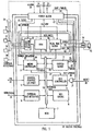
- the present invention is preferably embodied in a Secured Processing Unit (SPU) chip, a microprocessor designed especially for secure data processing.
- SPU Secured Processing Unit
- the SPU could be incorporated into an ATM card (and in ATM machines throughout the world), thereby implementing a worldwide distribution mechanism for secure financial transactions.
- a flexible architecture in accordance with the present invention permits extension and customization for specific applications without a compromise in security.
- One physical embodiment of this invention is a single-chip SPU that includes a 20-MHz 32-Bit CPU, based on the National Semiconductor NS32FV16 Advanced Imaging and Communications microprocessor, but lacking that chip's Digital Signal Processing (DSP) unit.
- DSP Digital Signal Processing
- the SPU's Micro Controller 3 is isolated from all off-chip input -- such input regulated by the External Bus Interface Block 9 and the general purpose I/O Port Block 1 --instead receiving programmed commands via an internal Data Bus 10 from the on-board ROM Block 7 .
- the ROM Block 7 is configured at 32 KBytes
- the battery-backed RAM Block 8 is configured at 4 KBytes.
- the Internal System Bus 10 carries all the major signals among the SPU peripherals, such as the address and data lines, read and write strobes, enable and reset signals, and the Micro Controller clock signal, CTTL 25 .
- the System Clock Block has a programmable internal high-frequency. oscillator, and is the source, through SYSCLK 35 , for the Micro Controller clock signal CTTL 25 , which governs all peripheral functions.
- the Real Time Clock 5 for the SPU follows the IEEE 1212 standard, which specifies control and status register architecture, and which builds upon and significantly enhances the UNIX time format (UNIX time being the number of seconds elapsed since January 1, 1970).
- the Real Time Clock 5 is implemented through a binary ripple counter which is driven via RTCLK 29 by an off-chip external 32.768 KHz quartz crystal 14 in conjunction with RTC Oscillator 14 circuitry.
- the Real Time Clock 5 provides UNIX time, and can implement a host of time-based functions and time limits under ROM Block 7 program control.
- One firmware routine stored in the ROM Block 9 cross-checks the System Clock 2 and Real Time Clock 5 so as to overcome tampering with the latter.
- the External Bus Interface Block 9 is the communications port to the host system. In one embodiment, it is the means for getting the application commands as well as data to and from the SPU, and is designed to match the ISA bus standard requirements.
- the Power Block 13 switches between system and battery power depending on system power availability. Power from an external battery (not shown) is supplied to the RTC Block 5 , the RAM Block 8 and a Status Register 11 through VPP 24 , as well as off-chip RAM (not shown) through VOUT 23 when system power is not available.
- the Power Block 13 also provides signals PWRGD 27 , DLY_PWRGD 26 and CHIP_PWRGD 28 , which, respectively, start the System Clock 2 , reset the Bus Controller 4 and enable the isolation of the battery-backed parts of the circuit from the non-battery backed parts through the Power Isolation 12 .
- a Silicon Firewall 20 protects the internal circuitry from any external asynchronous or otherwise anomalous signals, conditioning the inputs from the I/O Port Block 1 via PIN lines 32 or the External Bus Interface 9 via ADDR/DATA lines 33 , the RESET 30 to the Bus Controller 4 , as well as from a host of security detectors. Some internally generated signals, such as the output of the Real Time Clock 5 , are similarly conditioned.
- the Status Register 11 is the repository of all hardware detector signals arrayed through the device to detect various attempted security breaches. Detectors may include a Photo Detector 16 , Temperature Detector 17 , Metallization Layer Detector 18 and any Additional Detectors 19 (represented in ghost), for example: high/low voltage detectors, vibration detectors, sand detectors. Each of these detectors may convey one or more bits of information which, in one embodiment, are stored in the Status Register 11 .
- the Status Register 11 may also store internally generated signals, such as the ROLLOVER 34 signal from the Real Time Clock 5 and the Valid RAM and Time (VRT) bit, used to verify the integrity of the information stored in the RAM Block 8 and the time counter in the Real Time Clock 5 .
- a DES Engine 6 is provided as a cryptographic engine to encrypt and decrypt data using its DES algorithm.
- Alternative embodiments of cryptographic engines may be implemented entirely in hardware or in a combination of hardware and software, and may use other cryptological algorithms, including RSA or secret algorithms such as RC2, RC4, or Skipjack or combinations thereof.
- the DES Engine 6 receives keys and data for the cryptographic process from the RAM Block 8 under the control of the Micro Controller 3 .
- the data used could be application data supplied from the External Bus Interface 9 or protected data from the RAM Block 8 .
- the DES Block 6 performs a decryption of a 64-bit block in 18 clock cycles. Thus, with an SPU rated at 20 MHz, a single decryption will take approximately 90 ns, which amounts to a decryption rate of 8.9 Mbytes per second.
- the SPU receives "messages" in encrypted form.
- the cryptographic engine e.g. DES Engine 6
- the cryptographic engine uses keys, for example, "session keys” specific to a particular application transaction or “session”.
- the cryptographic engine is thus used to encrypt or decrypt the messages, or perform other cryptographic operations as is well-known in the art.
- the SPU also provides secure key transfer.
- the SPU can receive session keys in encrypted form and, treating them like messages, decrypt them with the cryptographic engine using the master key.
- the SPU can encrypt and send messages in a secure manner.
- the master key, the decrypted session keys and other sensitive information are stored in secure rewritable memory on the SPU, as described below.
- One embodiment of the present invention disables detection capability when the SPU is running on battery power VBAT 21 only.
- VDD 22 in the absence of system power, VDD 22 , non-battery backed parts of the SPU are temporarily powered through VBAT 21 .
- the OR gate 39 would send an ALARM 38 signal to the Power Block 13 .
- the system boundary is the silicon boundary, or equivalently, the pins of the SPU package.
- the components inside the system boundary are of two types: those responsible for maintaining the security of the system; and, those responsible for performing other functions. Separating the two types of components is the boundary called the security perimeter, with the area between the security perimeter and the silicon boundary called the silicon firewall.
- the silicon firewall's role is thus to defend the security perimeter.
- One aspect of this role is to prevent asynchronous inputs from outside the security perimeter reaching inside untreated; such inputs may drive the system into unpredictable and uncontrollable states.
- the Micro Controller 3 is one of the least trusted components in the SPU, precisely because it is difficult to verify all the multitudinous states of a micro controller. Consequently, the Micro Controller 3 in a SPU should be protected from asynchronous or otherwise abnormal inputs, i.e., signals which are outside the normal operating mode of the Micro Controller 3 . Examples of abnormal inputs are signals which have disallowed input levels (e.g., signals which have neither valid high nor valid low logic levels) and signals which have timing transitions which are out-of-specification. Not only do input signals external to the SPU need treatment, but all internal signals which are asynchronous to the Micro Controller must be treated by special protection circuitry.
- a common technique to prevent asynchronous and abnormal inputs is to equip all inputs to a semiconductor chip with Schmitt trigger devices coupled with latch circuits, which thereby ensure that signals cannot change state while they are being sampled by the semiconductor chip.
- Schmitt triggers it is difficult to fabricate Schmitt triggers.
- Schmitt triggers are slow because of hysteresis effects.
- the SPU according to the present invention uses a "Silicon Firewall" design to protect all interfaces to the Micro Controller 3 .
- One of the designs of the Silicon Firewall involves a state machine.
- a system clock compatible with PDPS faces a series of design considerations: cost, governmental regulatory compliance, printed circuit board area, power consumption and last, but most important, security.
- cost governmental regulatory compliance
- printed circuit board area governmental regulatory compliance
- power consumption last, but most important, security.
- the desire for high performance places a premium on clock speed, which is directly proportional thereto.
- the System Clock 2 represents a secure but somewhat inaccurate timing device, suitable for internal clocking of the Micro Controller 3 , but not for keeping UNIX time or to control timed and time-of-day events.
- the RTC Oscillator 14 is designed to produce a 32.768 KHz signal, RTCLK 29 , through use of an external quartz crystal 15 .
- OSC_ON 42 allows the oscillator to be stopped even though battery power is applied to the device. This prevents drain on the battery, as for example, while the system is in inventory before it is sold.
- secret information e.g., the decryption key
- the secret information will be destroyed if power to the SPU is turned off.
- an attacker can remove the SPU and at his leisure and by conventional means examine the information in the non-volatile memory.
- secret information is not loaded into the volatile memory properly, an attacker may still be able to examine the SPU while system power is turned off and obtain the secret information. This is because the secret information stored in conventional volatile memory may leave a residue on the dielectric material of the SPU, which the attacker can read to obtain the secret information even after power is turned off.
- the voltage level of the memory cells causes charge to build up in the dielectric material of the memory cells. If the same secret information is placed in the same memory location for an extended period of time, the dielectric material may be permanently affected by the charge of the memory cells. When this happens, it is possible to determine the secret information even after power is removed from the memory cells. Further, it is possible to artificially "age” the memory cells (so that the dielectric material can be permanently affected in less time) by elevating the voltage and changing the operating temperature of the SPU.
- One aspect of the present invention is an inverting key storage arrangement wherein the secret keys are periodically inverted. As a result, the net average charge across all memory cells is the same, thus leaving no signature of a specially-selected key in the dielectric material of the memory cells which would be amenable to detection.
- the inverting key storage arrangement is implemented in firmware.
- the firmware includes a key inverting routine which is executed in a predetermined time, e.g., once every 100 ms.
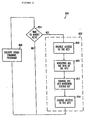
- a flowchart 800 which includes a key inverting routine 802 is shown in FIG. 2 .
- Flowchart 800 contains a decision block 804 which determines if it is time to branch to inverting routine 802 . If the answer is negative, programs in the firmware are executed (block 806 ). If it is time to execute the key inverting routine 802 , flowchart 800 branches to block 808 which causes all access to the keys to be disabled.
- the embedded controller then reads the key stored in volatile memory.
- the bits of the key are inverted and then stored back into memory (block 810 ).
- a key-inversion status bit is assigned to keep track of the status.
- the status of the key-inversion status bit is changed (block 812 ).
- the access to the key is now enabled (block 814 ).
- Flowchart 800 can now branch to block 806 to execute other firmware routines.
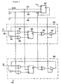
- FIG. 3 is a schematic diagram of such an arrangement 820 , which contains a JK flip flop 822 and a plurality of memory cells, such as cells 824 and 825 .
- Cell 824 contains two OR gates 827 and 828 , a JK flip flop 829 , a NOR gate 830 , an invertor 831 , and, a buffer 832 .
- a clock signal on line 834 is connected to the clock input of the two flip flops 822 and 829 .
- a Toggle/Load signal (T/L*) on line 835 is used to put the cells 824 and 825 in a toggle state when the signal is at a high value and the cells in a load state when the signal is at a low value.
- T/L* signal when the T/L* signal is low, the data on line 839 is loaded into memory cell 824 .
- the JK flip flop 829 When the T/L* signal is high, the JK flip flop 829 will toggle according to the clock signal on line 834 .
- a read signal on line 836 is coupled to the enable terminal of buffer 832 . The read signal allows the data stored in the memory cells to be read. The signal on line 836 indicates whether the output on line 839 is the original or the inverted signal.
- lightly doped N-type material exhibits a conductivity proportional to the amount of light to which the material is exposed.
- the Photo Detector 16 signal passes through the Silicon Firewall 20 before setting a bit in the Status Register 11 .
- a plurality of such detectors may be placed at strategic places within the SPU, which may be used to localize and further characterize the nature of any intrusion.
- the normal temperature operating range for the SPU is 0°C to 70°C. Any temperature above this range, in most applications, might well be considered to be the result of an intrusion attempt by an attacker, as for example, the heat generated by grinding away at the chip's outer layer.
- a substrate diode well-known to the art, should be sufficient for detecting temperature changes, although any other comparable device known to those of ordinary skill in the art for performing temperature measurement should suffice.
- the Temperature Detector 17 signal passes through the Silicon Firewall 20 before setting a bit in the Status Register 11 .
- Nothing in accordance with this invention precludes a multi-bit field characterizing a temperature scale, or a plurality of such detectors, to characterize any temperature differentials within the SPU.
Description
Claims (3)
- A secure chip for processing sensitive information and securing the information against potential attacks, the chip comprising:(a) a rewritable memory (8) for storing sensitive information having a substantially constant value;(b) a memory inverter (3) for periodically inverting the contents of each cell of the rewritable memory; and(c) a memory state bit for indicating whether the contents of each cell of the rewritable memory are in their actual state, or in the inverted state,whereby the contents of said rewritable memory contain effectively no residual electrical indication of the constant value of the sensitive information when said rewritable memory is powered off.
- A chip according to claim 1 wherein the memory inverter comprises firmware implementing a routine (800) which in each cycle of execution comprises:(a) disabling access to the sensitive information (808);(b) inverting all the bits of the sensitive information (810);(c) changing the state of the said memory state bit (812), and(d) enabling access to the sensitive information (814).
- A chip according to claim 1 wherein the memory cells each comprise a JK flip-flop (829) and the memory inverter comprises two OR gates (827, 828) which cause the flip-flop either to be loaded or to toggle, depending on the signal state of a line (835) coupled to the OR gates
Priority Applications (1)
| Application Number | Priority Date | Filing Date | Title |
|---|---|---|---|
| EP99115659A EP0965902A3 (en) | 1994-06-28 | 1995-05-05 | Secure data processor with cryptography and tamper detection |
Applications Claiming Priority (3)
| Application Number | Priority Date | Filing Date | Title |
|---|---|---|---|
| US267788 | 1994-06-28 | ||
| US08/267,788 US5533123A (en) | 1994-06-28 | 1994-06-28 | Programmable distributed personal security |
| PCT/US1995/005582 WO1996000953A2 (en) | 1994-06-28 | 1995-05-05 | Secure data processor with cryptography and tamper detection |
Related Child Applications (1)
| Application Number | Title | Priority Date | Filing Date |
|---|---|---|---|
| EP99115659A Division EP0965902A3 (en) | 1994-06-28 | 1995-05-05 | Secure data processor with cryptography and tamper detection |
Publications (2)
| Publication Number | Publication Date |
|---|---|
| EP0715733A1 EP0715733A1 (en) | 1996-06-12 |
| EP0715733B1 true EP0715733B1 (en) | 2000-12-20 |
Family
ID=23020117
Family Applications (2)
| Application Number | Title | Priority Date | Filing Date |
|---|---|---|---|
| EP99115659A Withdrawn EP0965902A3 (en) | 1994-06-28 | 1995-05-05 | Secure data processor with cryptography and tamper detection |
| EP95918978A Expired - Lifetime EP0715733B1 (en) | 1994-06-28 | 1995-05-05 | Secure data processor with cryptography and avoidance of unauthorized key readout |
Family Applications Before (1)
| Application Number | Title | Priority Date | Filing Date |
|---|---|---|---|
| EP99115659A Withdrawn EP0965902A3 (en) | 1994-06-28 | 1995-05-05 | Secure data processor with cryptography and tamper detection |
Country Status (5)
| Country | Link |
|---|---|
| US (1) | US5533123A (en) |
| EP (2) | EP0965902A3 (en) |
| KR (1) | KR100341665B1 (en) |
| DE (1) | DE69519662T2 (en) |
| WO (1) | WO1996000953A2 (en) |
Families Citing this family (235)
| Publication number | Priority date | Publication date | Assignee | Title |
|---|---|---|---|---|
| US5453601A (en) | 1991-11-15 | 1995-09-26 | Citibank, N.A. | Electronic-monetary system |
| US10361802B1 (en) | 1999-02-01 | 2019-07-23 | Blanding Hovenweep, Llc | Adaptive pattern recognition based control system and method |
| US5805706A (en) | 1996-04-17 | 1998-09-08 | Intel Corporation | Apparatus and method for re-encrypting data without unsecured exposure of its non-encrypted format |
| US5943297A (en) * | 1994-08-19 | 1999-08-24 | Hewlett-Packard Co. | Calendar clock circuit for computer workstations |
| US6154879A (en) * | 1994-11-28 | 2000-11-28 | Smarttouch, Inc. | Tokenless biometric ATM access system |
| US20040128249A1 (en) | 1994-11-28 | 2004-07-01 | Indivos Corporation, A Delaware Corporation | System and method for tokenless biometric electronic scrip |
| US6950810B2 (en) * | 1994-11-28 | 2005-09-27 | Indivos Corporation | Tokenless biometric electronic financial transactions via a third party identicator |
| US7248719B2 (en) * | 1994-11-28 | 2007-07-24 | Indivos Corporation | Tokenless electronic transaction system |
| US7613659B1 (en) | 1994-11-28 | 2009-11-03 | Yt Acquisition Corporation | System and method for processing tokenless biometric electronic transmissions using an electronic rule module clearinghouse |
| US7882032B1 (en) | 1994-11-28 | 2011-02-01 | Open Invention Network, Llc | System and method for tokenless biometric authorization of electronic communications |
| US6397198B1 (en) * | 1994-11-28 | 2002-05-28 | Indivos Corporation | Tokenless biometric electronic transactions using an audio signature to identify the transaction processor |
| US6658568B1 (en) | 1995-02-13 | 2003-12-02 | Intertrust Technologies Corporation | Trusted infrastructure support system, methods and techniques for secure electronic commerce transaction and rights management |
| US6157721A (en) | 1996-08-12 | 2000-12-05 | Intertrust Technologies Corp. | Systems and methods using cryptography to protect secure computing environments |
| US5943422A (en) | 1996-08-12 | 1999-08-24 | Intertrust Technologies Corp. | Steganographic techniques for securely delivering electronic digital rights management control information over insecure communication channels |
| US7133846B1 (en) | 1995-02-13 | 2006-11-07 | Intertrust Technologies Corp. | Digital certificate support system, methods and techniques for secure electronic commerce transaction and rights management |
| US6948070B1 (en) | 1995-02-13 | 2005-09-20 | Intertrust Technologies Corporation | Systems and methods for secure transaction management and electronic rights protection |
| DE69637733D1 (en) | 1995-02-13 | 2008-12-11 | Intertrust Tech Corp | SYSTEMS AND METHOD FOR SAFE TRANSMISSION |
| US5892900A (en) | 1996-08-30 | 1999-04-06 | Intertrust Technologies Corp. | Systems and methods for secure transaction management and electronic rights protection |
| US5796841A (en) * | 1995-08-21 | 1998-08-18 | Pitney Bowes Inc. | Secure user certification for electronic commerce employing value metering system |
| US5915020A (en) * | 1995-11-21 | 1999-06-22 | Hughes Electronics Corporation | Portable satellite earth station |
| US5720034A (en) * | 1995-12-07 | 1998-02-17 | Case; Jeffrey D. | Method for secure key production |
| US5774870A (en) | 1995-12-14 | 1998-06-30 | Netcentives, Inc. | Fully integrated, on-line interactive frequency and award redemption program |
| US7536331B1 (en) * | 1996-01-02 | 2009-05-19 | Robert W. Fletcher | Method for determining the risk associated with licensing or enforcing intellectual property |
| IL117085A (en) * | 1996-02-08 | 2005-07-25 | Milsys Ltd | Secure computer system |
| US20010011253A1 (en) | 1998-08-04 | 2001-08-02 | Christopher D. Coley | Automated system for management of licensed software |
| US5751595A (en) * | 1996-03-14 | 1998-05-12 | International Business Machines Corporation | Method for building and verifying authenticity of a rule system |
| US5883956A (en) * | 1996-03-28 | 1999-03-16 | National Semiconductor Corporation | Dynamic configuration of a secure processing unit for operations in various environments |
| US5761071A (en) * | 1996-07-27 | 1998-06-02 | Lexitech, Inc. | Browser kiosk system |
| US6078848A (en) * | 1996-07-27 | 2000-06-20 | Lexitech, Inc. | Browser kiosk system |
| US6993582B2 (en) * | 1996-07-30 | 2006-01-31 | Micron Technology Inc. | Mixed enclave operation in a computer network |
| US6272538B1 (en) * | 1996-07-30 | 2001-08-07 | Micron Technology, Inc. | Method and system for establishing a security perimeter in computer networks |
| FR2755267B1 (en) * | 1996-10-31 | 1998-12-24 | Solaic Sa | METHOD FOR SECURING AN AUTHENTICATION PROCESS USING A SECRET KEY ALGORITHM |
| US6028939A (en) * | 1997-01-03 | 2000-02-22 | Redcreek Communications, Inc. | Data security system and method |
| EP0856851B1 (en) * | 1997-01-30 | 2004-03-24 | Motorola, Inc. | Circuit and method of latching a bit line in a non-volatile memory |
| US6260149B1 (en) * | 1997-02-12 | 2001-07-10 | Intel Corporation | Method and apparatus for logic and power isolation during power management |
| US6216233B1 (en) | 1997-02-12 | 2001-04-10 | Intel Corporation | Maintaining a memory while in a power management mode |
| US5861662A (en) * | 1997-02-24 | 1999-01-19 | General Instrument Corporation | Anti-tamper bond wire shield for an integrated circuit |
| US5920861A (en) | 1997-02-25 | 1999-07-06 | Intertrust Technologies Corp. | Techniques for defining using and manipulating rights management data structures |
| US6330608B1 (en) | 1997-03-31 | 2001-12-11 | Stiles Inventions L.L.C. | Method and system of a computer system for establishing communications between a service provider and a central service factory and registry in a computer system |
| US6272637B1 (en) * | 1997-04-14 | 2001-08-07 | Dallas Semiconductor Corporation | Systems and methods for protecting access to encrypted information |
| US6101255A (en) * | 1997-04-30 | 2000-08-08 | Motorola, Inc. | Programmable cryptographic processing system and method |
| US6385723B1 (en) * | 1997-05-15 | 2002-05-07 | Mondex International Limited | Key transformation unit for an IC card |
| US7039802B1 (en) * | 1997-06-06 | 2006-05-02 | Thomson Licensing | Conditional access system for set-top boxes |
| US6453334B1 (en) | 1997-06-16 | 2002-09-17 | Streamtheory, Inc. | Method and apparatus to allow remotely located computer programs and/or data to be accessed on a local computer in a secure, time-limited manner, with persistent caching |
| EP0893751A1 (en) * | 1997-07-18 | 1999-01-27 | Irdeto B.V. | Integrated circuit and method for secure data processing by means of this integrated circuit |
| US6212635B1 (en) | 1997-07-18 | 2001-04-03 | David C. Reardon | Network security system allowing access and modification to a security subsystem after initial installation when a master token is in place |
| US6112181A (en) | 1997-11-06 | 2000-08-29 | Intertrust Technologies Corporation | Systems and methods for matching, selecting, narrowcasting, and/or classifying based on rights management and/or other information |
| JPH11191149A (en) * | 1997-12-26 | 1999-07-13 | Oki Electric Ind Co Ltd | Lsi for ic card and using method therefor |
| US7587044B2 (en) * | 1998-01-02 | 2009-09-08 | Cryptography Research, Inc. | Differential power analysis method and apparatus |
| EP1056015A4 (en) * | 1998-01-21 | 2005-01-05 | Tokyo Electron Ltd | Storage device, encrypting/decrypting device, and method for accessing nonvolatile memory |
| IL123028A (en) | 1998-01-22 | 2007-09-20 | Nds Ltd | Protection of data on media recording disks |
| US6292898B1 (en) | 1998-02-04 | 2001-09-18 | Spyrus, Inc. | Active erasure of electronically stored data upon tamper detection |
| US6980670B1 (en) * | 1998-02-09 | 2005-12-27 | Indivos Corporation | Biometric tokenless electronic rewards system and method |
| US6408391B1 (en) * | 1998-05-06 | 2002-06-18 | Prc Inc. | Dynamic system defense for information warfare |
| GB2381911B (en) * | 1998-05-06 | 2003-06-25 | Prc Inc | Dynamic system defense for information warfare |
| US6263447B1 (en) | 1998-05-21 | 2001-07-17 | Equifax Inc. | System and method for authentication of network users |
| CA2357007C (en) | 1998-05-21 | 2002-04-02 | Equifax Inc. | System and method for authentication of network users with preprocessing |
| AU4005999A (en) * | 1998-05-21 | 1999-12-06 | Equifax, Inc. | System and method for authentication of network users and issuing a digital certificate |
| ATE227445T1 (en) * | 1998-05-29 | 2002-11-15 | Infineon Technologies Ag | METHOD AND DEVICE FOR PROCESSING DATA |
| US20030118190A1 (en) * | 1998-05-29 | 2003-06-26 | Siemens Aktiengesellschaft | Method and apparatus for processing data where a part of the current supplied is supplied to an auxiliary circuit |
| WO2000005716A1 (en) * | 1998-07-22 | 2000-02-03 | Matsushita Electric Industrial Co., Ltd. | Digital data recording device and method for protecting copyright and easily reproducing encrypted digital data and computer readable recording medium recording program |
| US6374358B1 (en) * | 1998-08-05 | 2002-04-16 | Sun Microsystems, Inc. | Adaptive countermeasure selection method and apparatus |
| EP0984403A1 (en) * | 1998-09-01 | 2000-03-08 | Mindport B.V. | Security system |
| US6385727B1 (en) * | 1998-09-25 | 2002-05-07 | Hughes Electronics Corporation | Apparatus for providing a secure processing environment |
| CN1214304C (en) | 1998-11-05 | 2005-08-10 | 因芬尼昂技术股份公司 | Protection circuit for integrated circuit |
| US6594760B1 (en) * | 1998-12-21 | 2003-07-15 | Pitney Bowes Inc. | System and method for suppressing conducted emissions by a cryptographic device |
| US7209889B1 (en) | 1998-12-24 | 2007-04-24 | Henry Whitfield | Secure system for the issuance, acquisition, and redemption of certificates in a transaction network |
| US6553496B1 (en) * | 1999-02-01 | 2003-04-22 | Koninklijke Philips Electronics N.V. | Integration of security modules on an integrated circuit |
| US6145035A (en) * | 1999-02-25 | 2000-11-07 | Dallas Semiconductor Corporation | Card cradle system and method |
| EP1194884B1 (en) * | 1999-05-21 | 2003-04-09 | Infineon Technologies AG | Method for preventing the unauthorized use of chip cards |
| DE59914555D1 (en) * | 1999-06-01 | 2007-12-27 | Infineon Technologies Ag | protection circuit |
| US6598165B1 (en) * | 1999-06-18 | 2003-07-22 | Phoenix Technologies Ltd. | Secure memory |
| US6981155B1 (en) * | 1999-07-14 | 2005-12-27 | Symantec Corporation | System and method for computer security |
| AU5935400A (en) * | 1999-07-14 | 2001-01-30 | Recourse Technologies, Inc. | System and method for protecting a computer network against denial of service attacks |
| US7117532B1 (en) * | 1999-07-14 | 2006-10-03 | Symantec Corporation | System and method for generating fictitious content for a computer |
| US7203962B1 (en) * | 1999-08-30 | 2007-04-10 | Symantec Corporation | System and method for using timestamps to detect attacks |
| WO2001020559A1 (en) * | 1999-09-14 | 2001-03-22 | Neopost Inc. | Method and apparatus for user-sealing of secured postage printing equipment |
| DE19947574A1 (en) * | 1999-10-01 | 2001-04-12 | Giesecke & Devrient Gmbh | Process for securing a data storage |
| GB2355323A (en) * | 1999-10-05 | 2001-04-18 | Authoriszor Ltd | Information security profile and policy system |
| US6970850B1 (en) | 1999-10-27 | 2005-11-29 | Automated Business Companies | Proximity service provider system |
| US6091658A (en) * | 1999-11-01 | 2000-07-18 | Ford Global Technologies, Inc. | Nonvolatile memory implementation for electronic devices |
| DE19955601C2 (en) | 1999-11-18 | 2001-11-29 | Infineon Technologies Ag | Method for performing auto-refresh sequences on a DRAM |
| US6246254B1 (en) | 1999-12-06 | 2001-06-12 | International Business Machines Corporation | Method and circuit for providing copy protection in an application-specific integrated circuit |
| US6766455B1 (en) | 1999-12-09 | 2004-07-20 | Pitney Bowes Inc. | System and method for preventing differential power analysis attacks (DPA) on a cryptographic device |
| DE60035331T2 (en) * | 1999-12-09 | 2008-02-28 | Pitney Bowes, Inc., Stamford | A system and method for suppressing electromagnetic radiation of a cryptographic device having an integrated circuit |
| WO2001054057A1 (en) * | 2000-01-19 | 2001-07-26 | Infineon Technologies Ag | Integrated protective circuit |
| WO2001093167A1 (en) * | 2000-05-31 | 2001-12-06 | Indivos Corporation | Biometric financial transaction system and method |
| US9165323B1 (en) | 2000-05-31 | 2015-10-20 | Open Innovation Network, LLC | Biometric transaction system and method |
| US6976162B1 (en) | 2000-06-28 | 2005-12-13 | Intel Corporation | Platform and method for establishing provable identities while maintaining privacy |
| US7587368B2 (en) * | 2000-07-06 | 2009-09-08 | David Paul Felsher | Information record infrastructure, system and method |
| US6772361B1 (en) * | 2000-07-10 | 2004-08-03 | Advanced Micro Devices, Inc. | Real time clock (RTC) having several highly desirable timekeeping dependability and security attributes, and methods for accessing a register thereof |
| EP1410137A2 (en) * | 2000-08-09 | 2004-04-21 | Datawipe Management Services Limited | Personal data device and protection system and method for storing and protecting personal data |
| US20020049682A1 (en) * | 2000-09-01 | 2002-04-25 | Nobuko Yamamoto | Authentication certificate, authentication certificate issuance system, and authentication system |
| US7793111B1 (en) | 2000-09-28 | 2010-09-07 | Intel Corporation | Mechanism to handle events in a machine with isolated execution |
| US6618685B1 (en) * | 2000-10-17 | 2003-09-09 | Sun Microsystems, Inc. | Non-invasive testing of smart cards |
| US20030021417A1 (en) | 2000-10-20 | 2003-01-30 | Ognjen Vasic | Hidden link dynamic key manager for use in computer systems with database structure for storage of encrypted data and method for storage and retrieval of encrypted data |
| US7362868B2 (en) * | 2000-10-20 | 2008-04-22 | Eruces, Inc. | Hidden link dynamic key manager for use in computer systems with database structure for storage of encrypted data and method for storage and retrieval of encrypted data |
| US8831995B2 (en) | 2000-11-06 | 2014-09-09 | Numecent Holdings, Inc. | Optimized server for streamed applications |
| US7062567B2 (en) | 2000-11-06 | 2006-06-13 | Endeavors Technology, Inc. | Intelligent network streaming and execution system for conventionally coded applications |
| US7308713B1 (en) | 2000-11-22 | 2007-12-11 | Intel Corporation | Link-lock device and method of monitoring and controlling a link for failures and intrusions |
| US7316934B2 (en) * | 2000-12-18 | 2008-01-08 | Zavitan Semiconductors, Inc. | Personalized hardware |
| US7818808B1 (en) | 2000-12-27 | 2010-10-19 | Intel Corporation | Processor mode for limiting the operation of guest software running on a virtual machine supported by a virtual machine monitor |
| US7242921B2 (en) | 2000-12-29 | 2007-07-10 | Intel Corporation | Anonymous electronic transactions |
| DE10105987A1 (en) * | 2001-02-09 | 2002-08-29 | Infineon Technologies Ag | Data processing device |
| US20020114360A1 (en) * | 2001-02-20 | 2002-08-22 | Perlman Stephen G. | System and method for processing multiple broadcast multimedia streams |
| US7194618B1 (en) | 2001-03-05 | 2007-03-20 | Suominen Edwin A | Encryption and authentication systems and methods |
| US7181017B1 (en) | 2001-03-23 | 2007-02-20 | David Felsher | System and method for secure three-party communications |
| US7386129B2 (en) * | 2001-05-30 | 2008-06-10 | Digeo, Inc. | System and method for multimedia content simulcast |
| US7093277B2 (en) * | 2001-05-30 | 2006-08-15 | Digeo, Inc. | System and method for improved multi-stream multimedia transmission and processing |
| DE10131300B4 (en) * | 2001-07-02 | 2012-12-06 | Robert Bosch Gmbh | Method for protecting a microcomputer system against manipulation of data stored in a memory array and microcomputer system |
| JP2003051819A (en) * | 2001-08-08 | 2003-02-21 | Toshiba Corp | Microprocessor |
| US7463737B2 (en) | 2001-08-15 | 2008-12-09 | Digeo, Inc. | System and method for conditional access key encryption |
| US7024555B2 (en) | 2001-11-01 | 2006-04-04 | Intel Corporation | Apparatus and method for unilaterally loading a secure operating system within a multiprocessor environment |
| US20030097335A1 (en) * | 2001-11-21 | 2003-05-22 | International Business Machines Corporation | Secure method and system for determining charges and assuring privacy |
| US7644279B2 (en) * | 2001-12-05 | 2010-01-05 | Nvidia Corporation | Consumer product distribution in the embedded system market |
| US7231657B2 (en) * | 2002-02-14 | 2007-06-12 | American Management Systems, Inc. | User authentication system and methods thereof |
| US7124273B2 (en) | 2002-02-25 | 2006-10-17 | Intel Corporation | Method and apparatus for translating guest physical addresses in a virtual machine environment |
| US7631196B2 (en) | 2002-02-25 | 2009-12-08 | Intel Corporation | Method and apparatus for loading a trustable operating system |
| JP2003281071A (en) * | 2002-03-20 | 2003-10-03 | Seiko Epson Corp | Data transfer controller, electronic equipment and data transfer control method |
| US7069442B2 (en) | 2002-03-29 | 2006-06-27 | Intel Corporation | System and method for execution of a secured environment initialization instruction |
| US7840803B2 (en) * | 2002-04-16 | 2010-11-23 | Massachusetts Institute Of Technology | Authentication of integrated circuits |
| WO2003102510A2 (en) * | 2002-06-04 | 2003-12-11 | Nds Limited | Prevention of tampering in electronic devices |
| US6820177B2 (en) | 2002-06-12 | 2004-11-16 | Intel Corporation | Protected configuration space in a protected environment |
| US7392415B2 (en) * | 2002-06-26 | 2008-06-24 | Intel Corporation | Sleep protection |
| CA2901250A1 (en) * | 2002-07-12 | 2004-01-22 | Apple Inc. | Personal authentication software and systems for travel privilege assignation and verification |
| US7802108B1 (en) * | 2002-07-18 | 2010-09-21 | Nvidia Corporation | Secure storage of program code for an embedded system |
| KR100464598B1 (en) * | 2002-08-03 | 2005-01-03 | 한국정보보호진흥원 | The intrusion detection system and method unifying and resolving the misuses and anomalies of host |
| US6686247B1 (en) * | 2002-08-22 | 2004-02-03 | Intel Corporation | Self-aligned contacts to gates |
| EP1400887A1 (en) * | 2002-09-20 | 2004-03-24 | EM Microelectronic-Marin SA | Protecting device for electronic chip containing confidential data |
| JP4027776B2 (en) * | 2002-10-25 | 2007-12-26 | 有限会社クリプトソフトウエア | Data processing system, processing apparatus and computer program |
| JP4349788B2 (en) * | 2002-10-31 | 2009-10-21 | パナソニック株式会社 | Semiconductor integrated circuit device |
| JP4497874B2 (en) * | 2002-12-13 | 2010-07-07 | 株式会社ルネサステクノロジ | Semiconductor integrated circuit and IC card |
| US7900017B2 (en) | 2002-12-27 | 2011-03-01 | Intel Corporation | Mechanism for remapping post virtual machine memory pages |
| US7076802B2 (en) * | 2002-12-31 | 2006-07-11 | Intel Corporation | Trusted system clock |
| US20040128528A1 (en) | 2002-12-31 | 2004-07-01 | Poisner David I. | Trusted real time clock |
| WO2004063910A1 (en) * | 2003-01-10 | 2004-07-29 | Philips Intellectual Property & Standards Gmbh | Circuit arrangement and method for protecting electronic components against illicit manipulation |
| US7181016B2 (en) * | 2003-01-27 | 2007-02-20 | Microsoft Corporation | Deriving a symmetric key from an asymmetric key for file encryption or decryption |
| US9818136B1 (en) | 2003-02-05 | 2017-11-14 | Steven M. Hoffberg | System and method for determining contingent relevance |
| DE10317037A1 (en) * | 2003-04-14 | 2004-11-04 | Orga Kartensysteme Gmbh | Process for protecting data against unauthorized use on a mobile device |
| US6880752B2 (en) * | 2003-04-16 | 2005-04-19 | George V. Tarnovsky | System for testing, verifying legitimacy of smart card in-situ and for storing data therein |
| GB0310411D0 (en) * | 2003-05-07 | 2003-06-11 | Koninkl Philips Electronics Nv | Electronic device provided with cryptographic circuit and method of establishing the same |
| CA2527829C (en) | 2003-05-30 | 2016-09-27 | Privaris, Inc. | A man-machine interface for controlling access to electronic devices |
| US7366302B2 (en) * | 2003-08-25 | 2008-04-29 | Sony Corporation | Apparatus and method for an iterative cryptographic block |
| US8079034B2 (en) | 2003-09-15 | 2011-12-13 | Intel Corporation | Optimizing processor-managed resources based on the behavior of a virtual machine monitor |
| US7739521B2 (en) | 2003-09-18 | 2010-06-15 | Intel Corporation | Method of obscuring cryptographic computations |
| US20050080934A1 (en) | 2003-09-30 | 2005-04-14 | Cota-Robles Erik C. | Invalidating translation lookaside buffer entries in a virtual machine (VM) system |
| EP1536306A1 (en) | 2003-09-30 | 2005-06-01 | Broadcom Corporation | Proximity authentication system |
| FR2861474B1 (en) * | 2003-10-24 | 2007-04-27 | Atmel Corp | METHOD AND APPARATUS FOR A VARIABLE PROCESSING PERIOD IN AN INTEGRATED CIRCUIT |
| US8156343B2 (en) | 2003-11-26 | 2012-04-10 | Intel Corporation | Accessing private data about the state of a data processing machine from storage that is publicly accessible |
| US8037314B2 (en) | 2003-12-22 | 2011-10-11 | Intel Corporation | Replacing blinded authentication authority |
| FR2866450B1 (en) * | 2004-02-17 | 2006-06-02 | Enertec | "ANTI-COMPROMISE" TYPE DATA RECORDING CARTRIDGE AND CORRESPONDING ANTI-COMPROMISE METHOD |
| US7802085B2 (en) | 2004-02-18 | 2010-09-21 | Intel Corporation | Apparatus and method for distributing private keys to an entity with minimal secret, unique information |
| DE102004014435A1 (en) * | 2004-03-24 | 2005-11-17 | Siemens Ag | Arrangement with an integrated circuit |
| US7620949B2 (en) | 2004-03-31 | 2009-11-17 | Intel Corporation | Method and apparatus for facilitating recognition of an open event window during operation of guest software in a virtual machine environment |
| US20050229005A1 (en) * | 2004-04-07 | 2005-10-13 | Activcard Inc. | Security badge arrangement |
| DE102004028338A1 (en) * | 2004-06-11 | 2006-01-12 | Siemens Ag | tachograph |
| US7681042B2 (en) * | 2004-06-17 | 2010-03-16 | Eruces, Inc. | System and method for dis-identifying sensitive information and associated records |
| KR100636150B1 (en) * | 2004-07-01 | 2006-10-19 | 삼성전자주식회사 | Multimedia device having encryption module |
| US7119703B2 (en) * | 2004-08-26 | 2006-10-10 | Ftd Solutions Pte. Ltd. | Die anti-tampering sensor |
| US7818574B2 (en) * | 2004-09-10 | 2010-10-19 | International Business Machines Corporation | System and method for providing dynamically authorized access to functionality present on an integrated circuit chip |
| US7840962B2 (en) | 2004-09-30 | 2010-11-23 | Intel Corporation | System and method for controlling switching between VMM and VM using enabling value of VMM timer indicator and VMM timer value having a specified time |
| JP4391375B2 (en) * | 2004-09-30 | 2009-12-24 | フェリカネットワークス株式会社 | Information management apparatus and method, and program |
| US7015823B1 (en) | 2004-10-15 | 2006-03-21 | Systran Federal Corporation | Tamper resistant circuit boards |
| US8146078B2 (en) | 2004-10-29 | 2012-03-27 | Intel Corporation | Timer offsetting mechanism in a virtual machine environment |
| DE102004057259A1 (en) * | 2004-11-26 | 2006-06-01 | Robert Bosch Gmbh | Tamper-proof microcontroller system |
| US7188346B2 (en) * | 2004-11-29 | 2007-03-06 | International Business Machines Corporation | Method, system and program product for correlating data between operating environments |
| US8924728B2 (en) | 2004-11-30 | 2014-12-30 | Intel Corporation | Apparatus and method for establishing a secure session with a device without exposing privacy-sensitive information |
| US20060136717A1 (en) | 2004-12-20 | 2006-06-22 | Mark Buer | System and method for authentication via a proximate device |
| US8533777B2 (en) | 2004-12-29 | 2013-09-10 | Intel Corporation | Mechanism to determine trust of out-of-band management agents |
| US7395405B2 (en) | 2005-01-28 | 2008-07-01 | Intel Corporation | Method and apparatus for supporting address translation in a virtual machine environment |
| US7607020B2 (en) * | 2005-03-01 | 2009-10-20 | Adobe Systems Incorporated | Communication with an external source application |
| US8024523B2 (en) | 2007-11-07 | 2011-09-20 | Endeavors Technologies, Inc. | Opportunistic block transmission with time constraints |
| US8516583B2 (en) | 2005-03-31 | 2013-08-20 | Microsoft Corporation | Aggregating the knowledge base of computer systems to proactively protect a computer from malware |
| US7809957B2 (en) | 2005-09-29 | 2010-10-05 | Intel Corporation | Trusted platform module for generating sealed data |
| US8874477B2 (en) | 2005-10-04 | 2014-10-28 | Steven Mark Hoffberg | Multifactorial optimization system and method |
| IL171963A0 (en) * | 2005-11-14 | 2006-04-10 | Nds Ltd | Secure read-write storage device |
| US8195945B2 (en) * | 2005-12-01 | 2012-06-05 | Sony Mobile Communications Ab | Secure digital certificate storing scheme for flash memory and electronic apparatus |
| US8656191B2 (en) | 2005-12-23 | 2014-02-18 | Nagravision S.A. | Secure system-on-chip |
| EP1802030A1 (en) * | 2005-12-23 | 2007-06-27 | Nagracard S.A. | Secure system-on-chip |
| EP1811415A1 (en) * | 2005-12-23 | 2007-07-25 | Nagracard S.A. | Secure system-on-chip |
| US8959339B2 (en) | 2005-12-23 | 2015-02-17 | Texas Instruments Incorporated | Method and system for preventing unauthorized processor mode switches |
| US8014530B2 (en) | 2006-03-22 | 2011-09-06 | Intel Corporation | Method and apparatus for authenticated, recoverable key distribution with no database secrets |
| IL174784A0 (en) * | 2006-04-04 | 2006-12-31 | Nds Ltd | Robust cipher design |
| TWI506966B (en) | 2006-05-09 | 2015-11-01 | 內數位科技公司 | Secure time functionality for a wireless device |
| US8997255B2 (en) * | 2006-07-31 | 2015-03-31 | Inside Secure | Verifying data integrity in a data storage device |
| US8352752B2 (en) * | 2006-09-01 | 2013-01-08 | Inside Secure | Detecting radiation-based attacks |
| US20080061843A1 (en) * | 2006-09-11 | 2008-03-13 | Asier Goikoetxea Yanci | Detecting voltage glitches |
| US8239677B2 (en) * | 2006-10-10 | 2012-08-07 | Equifax Inc. | Verification and authentication systems and methods |
| US8447226B1 (en) | 2007-01-05 | 2013-05-21 | The Directv Group, Inc. | Portable satellite earth station and methods of using the same |
| US8286138B2 (en) * | 2007-01-30 | 2012-10-09 | Microsoft Corporation | Multi-threaded detection of a game software debugger |
| WO2008117467A1 (en) | 2007-03-27 | 2008-10-02 | Mitsubishi Electric Corporation | Secret information storage device, secret information erasing method, and secret information erasing program |
| AT505459B1 (en) * | 2007-06-25 | 2009-07-15 | Philipp Dr Tomsich | METHOD FOR ENSURING SAFE COMMUNICATION BETWEEN A TERMINAL AND SERVICE PROVIDERS IN A NETWORK |
| US8892738B2 (en) | 2007-11-07 | 2014-11-18 | Numecent Holdings, Inc. | Deriving component statistics for a stream enabled application |
| KR100954223B1 (en) * | 2007-11-22 | 2010-04-21 | 한국전자통신연구원 | Apparatus and method for security communication between encryption systems using Real Time Clock |
| FR2924262B1 (en) * | 2007-11-26 | 2009-12-11 | Sagem Securite | METHOD OF MASKING A PASSAGE AT THE END OF LIFE OF AN ELECTRONIC DEVICE AND DEVICE COMPRISING A CORRESPONDING CONTROL MODULE |
| US7953988B2 (en) * | 2008-01-10 | 2011-05-31 | Oracle America, Inc. | Modular tamper resistant enclosure for secure systems |
| GB0802741D0 (en) * | 2008-02-14 | 2008-03-26 | Wolfson Microelectronics Plc | Secure Clock |
| FR2927750B1 (en) * | 2008-02-15 | 2010-12-10 | Sagem Monetel | ELECTRONIC PAYMENT TERMINAL FOR SECURE DATA EXCHANGE ON AN OPEN NETWORK |
| US8819839B2 (en) * | 2008-05-24 | 2014-08-26 | Via Technologies, Inc. | Microprocessor having a secure execution mode with provisions for monitoring, indicating, and managing security levels |
| US8978132B2 (en) * | 2008-05-24 | 2015-03-10 | Via Technologies, Inc. | Apparatus and method for managing a microprocessor providing for a secure execution mode |
| US8789136B2 (en) * | 2008-09-02 | 2014-07-22 | Avaya Inc. | Securing a device based on atypical user behavior |
| FR2935817B1 (en) * | 2008-09-11 | 2011-12-09 | Oberthur Technologies | DATA PROCESSING METHOD AND ASSOCIATED DEVICE. |
| FR2935823B1 (en) * | 2008-09-11 | 2010-10-01 | Oberthur Technologies | METHOD AND DEVICE FOR PROTECTING A MICROCIRCUIT AGAINST ATTACKS. |
| US20100105997A1 (en) * | 2008-10-29 | 2010-04-29 | Medtronic, Inc. | Closed loop parameter adjustment for sensor modules of an implantable medical device |
| EP2199993A1 (en) * | 2008-12-17 | 2010-06-23 | Gemalto SA | Method and token for managing one processing relating to an application supported or to be supported by a token |
| US8677145B2 (en) * | 2009-02-27 | 2014-03-18 | Atmel Corporation | Single pin communication mechanism |
| FR2947361B1 (en) | 2009-06-29 | 2011-08-26 | Viaccess Sa | METHOD FOR DETECTING ATTACK ATTEMPT, RECORDING MEDIUM AND SECURITY PROCESSOR FOR SAID METHOD |
| EP2282279A1 (en) * | 2009-07-20 | 2011-02-09 | Nxp B.V. | Method and device for detection of light attacks |
| US8566940B1 (en) | 2009-11-25 | 2013-10-22 | Micron Technology, Inc. | Authenticated operations and event counters |
| US8255702B1 (en) * | 2009-12-03 | 2012-08-28 | Altera Corporation | Programmable logic device with improved security |
| US9525548B2 (en) | 2010-10-21 | 2016-12-20 | Microsoft Technology Licensing, Llc | Provisioning techniques |
| US8443224B2 (en) * | 2010-10-27 | 2013-05-14 | Freescale Semiconductor, Inc. | Apparatus and method for decoupling asynchronous clock domains |
| US8805434B2 (en) | 2010-11-23 | 2014-08-12 | Microsoft Corporation | Access techniques using a mobile communication device |
| US20120143769A1 (en) * | 2010-12-02 | 2012-06-07 | Microsoft Corporation | Commerce card |
| US9509686B2 (en) | 2010-12-03 | 2016-11-29 | Microsoft Technology Licensing, Llc | Secure element authentication |
| US9378379B1 (en) * | 2011-01-19 | 2016-06-28 | Bank Of America Corporation | Method and apparatus for the protection of information in a device upon separation from a network |
| US8996951B2 (en) | 2012-11-15 | 2015-03-31 | Elwha, Llc | Error correction with non-volatile memory on an integrated circuit |
| US9442854B2 (en) | 2012-11-15 | 2016-09-13 | Elwha Llc | Memory circuitry including computational circuitry for performing supplemental functions |
| US9582465B2 (en) | 2012-11-15 | 2017-02-28 | Elwha Llc | Flexible processors and flexible memory |
| US8925098B2 (en) * | 2012-11-15 | 2014-12-30 | Elwha Llc | Data security and access tracking in memory |
| US8966310B2 (en) | 2012-11-15 | 2015-02-24 | Elwha Llc | Redundancy for loss-tolerant data in non-volatile memory |
| US9323499B2 (en) | 2012-11-15 | 2016-04-26 | Elwha Llc | Random number generator functions in memory |
| US9026719B2 (en) | 2012-11-15 | 2015-05-05 | Elwha, Llc | Intelligent monitoring for computation in memory |
| FR2998695A1 (en) * | 2012-11-29 | 2014-05-30 | Altis Semiconductor Snc | Integrated circuit, has checking module arranged to control sensor or meter so as to deliver measurement representative of physical quantity, where module locks operation of circuit if measurement does not correspond to preset value |
| US10091204B1 (en) | 2013-12-31 | 2018-10-02 | EMC IP Holding Company LLC | Controlling user access to protected resource based on outcome of one-time passcode authentication token and predefined access policy |
| EP2942732A1 (en) * | 2014-05-07 | 2015-11-11 | Gemalto SA | Dynamic change of security configurations |
| CN107005669B (en) * | 2014-12-03 | 2020-05-05 | Nec显示器解决方案株式会社 | Display device and usage management method |
| CN105719183A (en) * | 2014-12-03 | 2016-06-29 | 阿里巴巴集团控股有限公司 | Directional transfer method and apparatus |
| US11487871B2 (en) * | 2015-01-31 | 2022-11-01 | San Diego Gas & Electric Company | Methods and systems for detecting and defending against invalid time signals |
| EP3262782B1 (en) | 2015-02-25 | 2022-07-27 | Private Machines Inc. | Anti-tamper system |
| DE102016117007A1 (en) * | 2016-09-09 | 2018-03-15 | Endress + Hauser Flowtec Ag | Method and system for verifying an electrical or electronic component |
| WO2018182635A1 (en) * | 2017-03-30 | 2018-10-04 | Blonder Tongue Laboratories, Inc. | Enterprise content gateway |
| FR3083412B1 (en) * | 2018-06-29 | 2021-09-24 | Youtransactor | METHOD OF PROTECTING A PAYMENT TERMINAL |
| US11050772B2 (en) | 2018-12-05 | 2021-06-29 | Bank Of America Corporation | Method and system for identification and prevention of profiling attacks in electronic authorization systems |
| US11321458B2 (en) | 2020-01-28 | 2022-05-03 | Nuvoton Technology Corporation | Secure IC with soft security countermeasures |
Family Cites Families (22)
| Publication number | Priority date | Publication date | Assignee | Title |
|---|---|---|---|---|
| US4446475A (en) * | 1981-07-10 | 1984-05-01 | Motorola, Inc. | Means and method for disabling access to a memory |
| US4521853A (en) * | 1982-06-30 | 1985-06-04 | Texas Instruments Incorporated | Secure microprocessor/microcomputer with secured memory |
| FR2536880B1 (en) * | 1982-11-30 | 1987-05-07 | Bull Sa | MICROPROCESSOR DESIGNED IN PARTICULAR FOR EXECUTING THE CALCULATION ALGORITHMS OF A PUBLIC KEY ENCRYPTION SYSTEM |
| DE3483410D1 (en) * | 1983-10-14 | 1990-11-22 | Toshiba Kawasaki Kk | ONE-CHIP MICROCOMPUTER WITH LOCKABLE FUNCTION OF THE PROGRAM MEMORY. |
| DE3347483A1 (en) * | 1983-12-29 | 1985-07-11 | GAO Gesellschaft für Automation und Organisation mbH, 8000 München | DEVICE FOR SECURING SECRET INFORMATION |
| US4598170A (en) * | 1984-05-17 | 1986-07-01 | Motorola, Inc. | Secure microprocessor |
| US4593384A (en) * | 1984-12-21 | 1986-06-03 | Ncr Corporation | Security device for the secure storage of sensitive data |
| GB2182176B (en) * | 1985-09-25 | 1989-09-20 | Ncr Co | Data security device for protecting stored data |
| GB2182467B (en) * | 1985-10-30 | 1989-10-18 | Ncr Co | Security device for stored sensitive data |
| GB2195478B (en) * | 1986-09-24 | 1990-06-13 | Ncr Co | Security device for sensitive data |
| US4860351A (en) * | 1986-11-05 | 1989-08-22 | Ibm Corporation | Tamper-resistant packaging for protection of information stored in electronic circuitry |
| US5117457A (en) * | 1986-11-05 | 1992-05-26 | International Business Machines Corp. | Tamper resistant packaging for information protection in electronic circuitry |
| JPS63293664A (en) * | 1987-05-27 | 1988-11-30 | Sharp Corp | Electronic equipment |
| US5185717A (en) * | 1988-08-05 | 1993-02-09 | Ryoichi Mori | Tamper resistant module having logical elements arranged in multiple layers on the outer surface of a substrate to protect stored information |
| US4933898A (en) * | 1989-01-12 | 1990-06-12 | General Instrument Corporation | Secure integrated circuit chip with conductive shield |
| US5083293A (en) * | 1989-01-12 | 1992-01-21 | General Instrument Corporation | Prevention of alteration of data stored in secure integrated circuit chip memory |
| US5189700A (en) * | 1989-07-05 | 1993-02-23 | Blandford Robert R | Devices to (1) supply authenticated time and (2) time stamp and authenticate digital documents |
| US5027397A (en) * | 1989-09-12 | 1991-06-25 | International Business Machines Corporation | Data protection by detection of intrusion into electronic assemblies |
| CA2067331A1 (en) * | 1989-10-03 | 1991-04-04 | Joseph Unsworth | Electro-active cradle circuits for the detection of access or penetration |
| US5053992A (en) * | 1990-10-04 | 1991-10-01 | General Instrument Corporation | Prevention of inspection of secret data stored in encapsulated integrated circuit chip |
| US5457748A (en) * | 1992-11-30 | 1995-10-10 | Motorola, Inc. | Method and apparatus for improved security within encrypted communication devices |
| US5444780A (en) * | 1993-07-22 | 1995-08-22 | International Business Machines Corporation | Client/server based secure timekeeping system |
-
1994
- 1994-06-28 US US08/267,788 patent/US5533123A/en not_active Expired - Lifetime
-
1995
- 1995-05-05 KR KR1019960701013A patent/KR100341665B1/en not_active IP Right Cessation
- 1995-05-05 WO PCT/US1995/005582 patent/WO1996000953A2/en active IP Right Grant
- 1995-05-05 DE DE69519662T patent/DE69519662T2/en not_active Expired - Lifetime
- 1995-05-05 EP EP99115659A patent/EP0965902A3/en not_active Withdrawn
- 1995-05-05 EP EP95918978A patent/EP0715733B1/en not_active Expired - Lifetime
Also Published As
| Publication number | Publication date |
|---|---|
| WO1996000953A2 (en) | 1996-01-11 |
| KR960705284A (en) | 1996-10-09 |
| KR100341665B1 (en) | 2002-11-29 |
| EP0965902A2 (en) | 1999-12-22 |
| DE69519662D1 (en) | 2001-01-25 |
| US5533123A (en) | 1996-07-02 |
| WO1996000953A3 (en) | 1996-02-15 |
| EP0715733A1 (en) | 1996-06-12 |
| EP0965902A3 (en) | 2005-12-21 |
| DE69519662T2 (en) | 2001-05-23 |
Similar Documents
| Publication | Publication Date | Title |
|---|---|---|
| EP0715733B1 (en) | Secure data processor with cryptography and avoidance of unauthorized key readout | |
| EP0743602B1 (en) | Circuit device for function usage control in an integrated circuit | |
| Maes et al. | Intrinsic PUFs from flip-flops on reconfigurable devices | |
| Bar-El et al. | The sorcerer's apprentice guide to fault attacks | |
| US6345359B1 (en) | In-line decryption for protecting embedded software | |
| US8352752B2 (en) | Detecting radiation-based attacks | |
| US5828753A (en) | Circuit and method for ensuring interconnect security within a multi-chip integrated circuit package | |
| US7218567B1 (en) | Method and apparatus for the protection of sensitive data within an integrated circuit | |
| EP2115655B1 (en) | Virtual secure on-chip one time programming | |
| JP3866105B2 (en) | Microprocessor device with encryption function | |
| US7005733B2 (en) | Anti tamper encapsulation for an integrated circuit | |
| US6330668B1 (en) | Integrated circuit having hardware circuitry to prevent electrical or thermal stressing of the silicon circuitry | |
| US20020166058A1 (en) | Semiconductor integrated circuit on IC card protected against tampering | |
| Duncan et al. | FPGA bitstream security: a day in the life | |
| US7127620B2 (en) | Power analysis resistant coding device | |
| CA2737145A1 (en) | Secure communication interface for secure multi-processor system | |
| US11930098B2 (en) | Devices and methods for the detection and localization of fault injection attacks | |
| EP1032869A1 (en) | An apparatus for providing a secure processing environment | |
| Guilley et al. | SoC security: a war against side-channels | |
| WO1999035554A2 (en) | Method and apparatus for protection of data on an integrated circuit by using memory cells to detect tampering | |
| US20030133241A1 (en) | Method and arrangement for protecting digital parts of circuits | |
| Tehranipoor et al. | Tamper Detection | |
| Zhang | Combinational Logic Binding for FPGA System Security | |
| Biomatica | Zyt Cryptographic Module Security Policy | |
| Choukri et al. | Fault Attacks Fault Attacks |
Legal Events
| Date | Code | Title | Description |
|---|---|---|---|
| PUAI | Public reference made under article 153(3) epc to a published international application that has entered the european phase |
Free format text: ORIGINAL CODE: 0009012 |
|
| 17P | Request for examination filed |
Effective date: 19960312 |
|
| AK | Designated contracting states |
Kind code of ref document: A1 Designated state(s): DE FR GB |
|
| 17Q | First examination report despatched |
Effective date: 19990702 |
|
| GRAG | Despatch of communication of intention to grant |
Free format text: ORIGINAL CODE: EPIDOS AGRA |
|
| RIC1 | Information provided on ipc code assigned before grant |
Free format text: 7G 06F 12/14 A, 7G 06F 1/00 B |
|
| RTI1 | Title (correction) |
Free format text: SECURE DATA PROCESSOR WITH CRYPTOGRAPHY AND AVOIDANCE OF UNAUTHORIZED KEY READOUT |
|
| GRAG | Despatch of communication of intention to grant |
Free format text: ORIGINAL CODE: EPIDOS AGRA |
|
| GRAH | Despatch of communication of intention to grant a patent |
Free format text: ORIGINAL CODE: EPIDOS IGRA |
|
| GRAH | Despatch of communication of intention to grant a patent |
Free format text: ORIGINAL CODE: EPIDOS IGRA |
|
| GRAA | (expected) grant |
Free format text: ORIGINAL CODE: 0009210 |
|
| AK | Designated contracting states |
Kind code of ref document: B1 Designated state(s): DE FR GB |
|
| PG25 | Lapsed in a contracting state [announced via postgrant information from national office to epo] |
Ref country code: FR Free format text: LAPSE BECAUSE OF FAILURE TO SUBMIT A TRANSLATION OF THE DESCRIPTION OR TO PAY THE FEE WITHIN THE PRESCRIBED TIME-LIMIT Effective date: 20001220 |
|
| REF | Corresponds to: |
Ref document number: 69519662 Country of ref document: DE Date of ref document: 20010125 |
|
| PG25 | Lapsed in a contracting state [announced via postgrant information from national office to epo] |
Ref country code: GB Free format text: LAPSE BECAUSE OF NON-PAYMENT OF DUE FEES Effective date: 20010505 |
|
| EN | Fr: translation not filed | ||
| PLBE | No opposition filed within time limit |
Free format text: ORIGINAL CODE: 0009261 |
|
| STAA | Information on the status of an ep patent application or granted ep patent |
Free format text: STATUS: NO OPPOSITION FILED WITHIN TIME LIMIT |
|
| 26N | No opposition filed | ||
| GBPC | Gb: european patent ceased through non-payment of renewal fee |
Effective date: 20010505 |
|
| PGFP | Annual fee paid to national office [announced via postgrant information from national office to epo] |
Ref country code: DE Payment date: 20120529 Year of fee payment: 18 |
|
| REG | Reference to a national code |
Ref country code: DE Ref legal event code: R082 Ref document number: 69519662 Country of ref document: DE |
|
| PG25 | Lapsed in a contracting state [announced via postgrant information from national office to epo] |
Ref country code: DE Free format text: LAPSE BECAUSE OF NON-PAYMENT OF DUE FEES Effective date: 20131203 |
|
| REG | Reference to a national code |
Ref country code: DE Ref legal event code: R119 Ref document number: 69519662 Country of ref document: DE Effective date: 20131203 |