EP0719002A1 - Carrier recovery processor - Google Patents
Carrier recovery processor Download PDFInfo
- Publication number
- EP0719002A1 EP0719002A1 EP94203725A EP94203725A EP0719002A1 EP 0719002 A1 EP0719002 A1 EP 0719002A1 EP 94203725 A EP94203725 A EP 94203725A EP 94203725 A EP94203725 A EP 94203725A EP 0719002 A1 EP0719002 A1 EP 0719002A1
- Authority
- EP
- European Patent Office
- Prior art keywords
- vector
- signal processor
- signal
- phase angle
- processor module
- Prior art date
- Legal status (The legal status is an assumption and is not a legal conclusion. Google has not performed a legal analysis and makes no representation as to the accuracy of the status listed.)
- Granted
Links
Images

Classifications
-
- H—ELECTRICITY
- H04—ELECTRIC COMMUNICATION TECHNIQUE
- H04L—TRANSMISSION OF DIGITAL INFORMATION, e.g. TELEGRAPHIC COMMUNICATION
- H04L27/00—Modulated-carrier systems
- H04L27/26—Systems using multi-frequency codes
- H04L27/2601—Multicarrier modulation systems
- H04L27/2647—Arrangements specific to the receiver only
- H04L27/2655—Synchronisation arrangements
- H04L27/2657—Carrier synchronisation
-
- H—ELECTRICITY
- H04—ELECTRIC COMMUNICATION TECHNIQUE
- H04L—TRANSMISSION OF DIGITAL INFORMATION, e.g. TELEGRAPHIC COMMUNICATION
- H04L27/00—Modulated-carrier systems
- H04L27/26—Systems using multi-frequency codes
- H04L27/2601—Multicarrier modulation systems
- H04L27/2647—Arrangements specific to the receiver only
- H04L27/2655—Synchronisation arrangements
- H04L27/2668—Details of algorithms
- H04L27/2673—Details of algorithms characterised by synchronisation parameters
- H04L27/2675—Pilot or known symbols
-
- H—ELECTRICITY
- H04—ELECTRIC COMMUNICATION TECHNIQUE
- H04L—TRANSMISSION OF DIGITAL INFORMATION, e.g. TELEGRAPHIC COMMUNICATION
- H04L27/00—Modulated-carrier systems
- H04L27/32—Carrier systems characterised by combinations of two or more of the types covered by groups H04L27/02, H04L27/10, H04L27/18 or H04L27/26
- H04L27/34—Amplitude- and phase-modulated carrier systems, e.g. quadrature-amplitude modulated carrier systems
- H04L27/38—Demodulator circuits; Receiver circuits
- H04L27/3818—Demodulator circuits; Receiver circuits using coherent demodulation, i.e. using one or more nominally phase synchronous carriers
Definitions
- the present invention relates to a signal processor module adapted to check if a vector representing a received signal, is located in a predetermined zone of a signal vector plane.
- Such a signal processor module is already known in the art, e.g. from the US patent 4,697,227.
- the signal processor which is referred to as tracking system, checks if the received vector is located in a square centered around the constellation point i.e. the end point of an expected vector, representing a signal which should have been received instead of the really received one.
- the signal processor uses the position of the received vector with respect to the expected vector to determine the attenuation and frequency offset to which the signal represented by the received vector has been submitted. More in particular, the averaged phase angle difference between the received and expected vector is indicative of this frequency offset.
- phase angle difference may be very high e.g. in the case of the end point of the received vector lying in a corner of the square.
- An occasional high phase angle difference may result in the above mentioned averaged phase angle difference which wrongly indicates a certain frequency offset.
- An object of the present invention is to provide a signal processor module of the above known type but which is adapted to check if the received vector is located in a predetermined zone having such a shape that the above mentioned drawback is overcome.
- said signal processor module includes first checking means to check if said vector is located in a first zone delimited by successive orthogonal line segments, second checking means to check if said vector is located in a second zone delimited by two lines, and gating means coupled to said first and second checking means to determine if said vector is located in said predetermined zone equal to the intersection zone of said first and second zones.
- the two lines may be chosen so that the vectors lying in the intersection zone necessarily have a limited phase angle difference.
- a characteristic feature of the present invention is that said first checking means performs said check by comparing orthogonal coordinate values representing said vector with orthogonal coordinate values of corner points of said first zone.
- said signal processor module further includes conversion means intercoupling said first and said second checking means and adapted to convert said orthogonal coordinate values of said vector to a phase angle value indicative of the phase angle difference between said vector and a predetermined vector.
- the orthogonal coordinates are converted to an angular coordinate i.e. the phase angle difference, so that the second zone may be determined based on the above angular coordinate.
- Yet another characteristic feauture of the present invention is that said two line are secant in the origin of said signal vector plane and that said predetermined vector lies on the bissectrice of said two secant lines.
- the second zone is shaped symmetrically with respect to the predetermined vector.
- said second checking means performs said check by comparing said phase angle value with the phase angle between said bissectrice and one of said secant lines, and with the opposite of said phase angle and that said first and said second checking means have respective first and second control outputs indicating if said vector is located within said first and second zones respectively, and that both said control outputs are gated by said gating means.
- the signal processor module provides an averaged phase angle value due to the fact that said signal processor module further includes averaging means (AVF) coupled to said second checking means and to an output of said gating means, said averaging means being adapted to average said phase angle value according to said output of said gating means.
- AMF averaging means
- the signal processor shown therein includes the cascade connection of a sampling unit SU having an input terminal IT, a Fast Fourier Transform unit FFTU having an output terminal OT, a signal processor unit SPU, an averaging filter AVF and a microprocessor P.
- a first output terminal T5 of P is fed back to a control terminal T7 of SU via a voltage controlled oscillator VCO and a second output terminal T6 of P is directly fed back to a control terminal T8 of FFTU.
- An output terminal T3 of SPU is connected to a control terminal T4 of AVF.
- the signal processor module according to the invention is constituted by the cascade connection of the SPU unit and the AVF filter.
- the signal processor unit SPU includes the cascade connection of a first comparator circuit CM1, a convertor circuit COM and a second comparator circuit CM2.
- An output terminal T1 of CM1 and an output terminal T2 of CM2 constitute the inputs of an AND-gate AND having an output terminal constituing terminal T3 of SPU.
- the signal processor shown in Fig 1 is adapted to process a so called Discrete Multi Tone or DMT input signal.
- a DMT signal comprises a number of quadrature amplitude modulated frequencies or tones occurring during successive equal symbol intervals.
- the DMT technique is well described in the above US patent.
- One of the above tones or Pilot tone is used by the signal processor to track the starting points of each symbol interval.
- the signal processor samples the DMT input signal received at IT and it is of the utmost importance that predetermined sampling instants coincide with the starting points of the symbol intervals. To this end, the signal processor adjusts the sample frequency Fs in the sample unit SU and corrects possible misalignment of predetermined sample instants with the above starting points of the symbol intervals, in the Fast Fourier Transform unit FFTU.
- the averaged phase angle error is normally used to perform the latter correction.
- This averaged phase angle error also indicates a possible sample frequency error which may be accordingly adjusted via the VCO.
- the signal processor may wrongly correct a phase error or a frequency error and as a consequence the overal operation of the signal processor may be erroneous.
- the signal processor module according to the present invention solves this problem through providing an averaged phase angle error wich not sensitive to occasional large phase errors of the pilot tone.
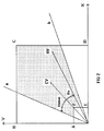
- a vector EV represents the expected Pilot Tone in a QAM signal vector plane having a orthogonal X and Y axis.
- a vector RV represent the Pilot Tone which is received at the input terminal IT.
- the hatched zone is the intersection of a first zone ABCDEF, delimited by consecutive orthogonal line segments, and a second zone ab, delimited by two secant lines of which the bissectrice coincides with an expected vector EV which represents the Pilot Tone which should have been received under ideal conditions.
- Da is the phase angle difference between EV and RV and Damax is half of the angle between the two secant lines a and b.
- the DMT input signal which is applied to the signal processor input IT is sampled at a sample frequency Fs in the sample unit SU.
- This sample frequency Fs is regulated via the control input T7 which constitutes an oscillator output of the voltage controlled oscillator VCO.
- the thus sampled DMT input signal is supplied during the symbol intervals by the sample unit SU to the Fast Fourier Transform unit FFTU which calculates the orthogonal coordinates in the QAM signal plane of each vector representing a tone present in the DMT input signal during such a symbol interval.
- the FFT unit calculates the X,Y orthogonal coordinates in the QAM signal vector plane shown in Fig 2.
- These orthogonal coordinates of the received pilot tone vector RV are transferred to the signal processor unit SPU, whereas the orthogonal coordinates of the vectors representing all the other tones present in the DMT input signal are forwarded to the output terminal OT.
- the signal processor unit SPU calculates the phase angle difference Da between the received Pilot Tone vector RV and the expected pilot tone vector EV.
- the signal processor unit SPU further indicates by a high/low signal at the T3 output terminal that the received Pilot Tone vector RV is/is not located in the hatched intersection of the first and second zones shown in Fig 2.
- the signal processor unit SPU provides the above phase angle difference Da calculated for each symbol interval of the DMT input signal, to the averaging filter AVF which, accordingly, supplies an averaged phase angle difference ADa to the microprocessor P.
- ADa is the averaged value of Da over the last N symbol intervals for which the signal at the control terminal T4 of AVF was set high by the output terminal T3 of SPU. This means that a phase angle difference Da is ignored by the averaging filter AVF when the signal at T3 is set low by the signal processor unit SPU.
- the microprocessor evaluates the averaged phase angle difference ADa and thereby generates a control voltage at its output terminal T5 and provides a control signal at its output terminal T6.
- the control voltage controls the output oscillator frequency of the VCO and the control signal is used by FFTU to compensate for the above mentioned misalignment of some predetermined sample instants with respect to the starting points of the symbol intervals. It is beyond the scope of the invention to describe how this control voltage and this control signal are determined from ADa, and how FFTU performs the compensation based on the control signal.
- the first comparator and storage circuit CM1 compares the orthogonal coordinates of the vector RV supplied by FFTU, with the orthogonal coordinates of the corner points A,B,C,D,E and F of the first zone, these coordinates being stored (not shown) in CM1.
- the signal at the output terminal T1 of CM1 is set high/low.
- the circuit CM1 passes the coordinates of the vector RV ot the conversion and storage circuit COM which calculates the phase angle difference Da between the expected pilot vector EV and the received pilot vector RV.
- the orthogonal coordinates of the vector EV are stored (not shown) in COM and the calculation of Da is straight forward for a person skilled in the art.
- the circuit COM passes the coordinates of the vector RV to the second comparator and storage circuit CM2 which compares Da with the values +/-Damax.
- the output terminal CT2 of CM2 is set high/low when the condition -Damax ⁇ Da ⁇ +Damax is/is not fullfilled.
- the signal at terminal T2 is set high/low if vector RV is/is not located in the second zone.
- the circuit CM2 finally forwards the calculated phase angle difference Da to the averaging filter AVF.
- the signals at terminals T1 and T2 are gated in the AND-gate AND and thus the signal at the terminal T3 is thus set high/low if the vector RV is/is not located in the intersection of the first and second zones.
- phase angle difference Da may be approximated using more simple calculations. For instance, when the vectors EV and RV are located in the first quadrant of the signal vector plane, Da ⁇ + (X(EV)-X(RV)) - (Y(EV)-Y(RV)) ; X(EV), Y(EV), X(RV) and Y(RV) being the X and Y coordinates of the vectors EV and RV respectively, in the signal vector plane.
- the two lines a and b may be parrallel to the vector EV or secant in a point different from the origin of the signal vector plane.
- the advantage of this approximation is that the implementation of the conversion circuit COM is less complex.
Abstract
Description
- The present invention relates to a signal processor module adapted to check if a vector representing a received signal, is located in a predetermined zone of a signal vector plane.
- Such a signal processor module is already known in the art, e.g. from the US patent 4,697,227. Therein, the signal processor which is referred to as tracking system, checks if the received vector is located in a square centered around the constellation point i.e. the end point of an expected vector, representing a signal which should have been received instead of the really received one. The signal processor uses the position of the received vector with respect to the expected vector to determine the attenuation and frequency offset to which the signal represented by the received vector has been submitted. More in particular, the averaged phase angle difference between the received and expected vector is indicative of this frequency offset.
- A major drawback of the shape of the square is that the phase angle difference may be very high e.g. in the case of the end point of the received vector lying in a corner of the square. An occasional high phase angle difference may result in the above mentioned averaged phase angle difference which wrongly indicates a certain frequency offset. Although the US patent mentions arbitrarily shaped zones, it is not described how a zone needs to be shaped in order to overcome the above mentioned drawback, nor is it described how such a zone can be achieved.
- An object of the present invention is to provide a signal processor module of the above known type but which is adapted to check if the received vector is located in a predetermined zone having such a shape that the above mentioned drawback is overcome.
- According to the invention, this object is achieved due to the fact that said signal processor module includes first checking means to check if said vector is located in a first zone delimited by succesive orthogonal line segments, second checking means to check if said vector is located in a second zone delimited by two lines, and gating means coupled to said first and second checking means to determine if said vector is located in said predetermined zone equal to the intersection zone of said first and second zones.
- Indeed, the two lines may be chosen so that the vectors lying in the intersection zone necessarily have a limited phase angle difference.
- A characteristic feature of the present invention is that said first checking means performs said check by comparing orthogonal coordinate values representing said vector with orthogonal coordinate values of corner points of said first zone.
- Another characteristic feauture of the present ivention is that said signal processor module further includes conversion means intercoupling said first and said second checking means and adapted to convert said orthogonal coordinate values of said vector to a phase angle value indicative of the phase angle difference between said vector and a predetermined vector.
- In this way, the orthogonal coordinates are converted to an angular coordinate i.e. the phase angle difference, so that the second zone may be determined based on the above angular coordinate.
- Yet another characteristic feauture of the present invention is that said two line are secant in the origin of said signal vector plane and that said predetermined vector lies on the bissectrice of said two secant lines.
- In this way the second zone is shaped symmetrically with respect to the predetermined vector.
- Further characteristic features of the present invention are that said second checking means performs said check by comparing said phase angle value with the phase angle between said bissectrice and one of said secant lines, and with the opposite of said phase angle and that said first and said second checking means have respective first and second control outputs indicating if said vector is located within said first and second zones respectively, and that both said control outputs are gated by said gating means.
- Finally the signal processor module according to the invention provides an averaged phase angle value due to the fact that said signal processor module further includes averaging means (AVF) coupled to said second checking means and to an output of said gating means, said averaging means being adapted to average said phase angle value according to said output of said gating means.
- The above mentioned and other objects and features of the invention will become more apparent and the invention itself will be best understood by referring to the following description of an embodiment taken in conjunction with the accompanying drawings wherein :
- Fig 1 represents a signal processor including a signal processor module according to the present invention;
- Fig 2 shows the hatched intersection zone of two zones within a Quadrature Amplitude Modulation or QAM signal vector plane.
- Referring to Fig 1, the signal processor shown therein includes the cascade connection of a sampling unit SU having an input terminal IT, a Fast Fourier Transform unit FFTU having an output terminal OT, a signal processor unit SPU, an averaging filter AVF and a microprocessor P. A first output terminal T5 of P is fed back to a control terminal T7 of SU via a voltage controlled oscillator VCO and a second output terminal T6 of P is directly fed back to a control terminal T8 of FFTU. An output terminal T3 of SPU is connected to a control terminal T4 of AVF. The signal processor module according to the invention is constituted by the cascade connection of the SPU unit and the AVF filter.
- More in detail, the signal processor unit SPU includes the cascade connection of a first comparator circuit CM1, a convertor circuit COM and a second comparator circuit CM2. An output terminal T1 of CM1 and an output terminal T2 of CM2 constitute the inputs of an AND-gate AND having an output terminal constituing terminal T3 of SPU.
- The signal processor shown in Fig 1 is adapted to process a so called Discrete Multi Tone or DMT input signal. A DMT signal comprises a number of quadrature amplitude modulated frequencies or tones occurring during successive equal symbol intervals. The DMT technique is well described in the above US patent. One of the above tones or Pilot tone is used by the signal processor to track the starting points of each symbol interval. As is explained later on, the signal processor samples the DMT input signal received at IT and it is of the utmost importance that predetermined sampling instants coincide with the starting points of the symbol intervals. To this end, the signal processor adjusts the sample frequency Fs in the sample unit SU and corrects possible misalignment of predetermined sample instants with the above starting points of the symbol intervals, in the Fast Fourier Transform unit FFTU.
- It is well know to a person skilled in the art how the above misalignment and sample frequency are corrected using the Pilot Tone and therefor only the basic idea behind it is explained hereafter. Let's e.g. suppose that the Pilot Tone


- Referring to Fig 2, a vector EV represents the expected Pilot Tone in a QAM signal vector plane having a orthogonal X and Y axis. A vector RV represent the Pilot Tone which is received at the input terminal IT. The hatched zone is the intersection of a first zone ABCDEF, delimited by consecutive orthogonal line segments, and a second zone ab, delimited by two secant lines of which the bissectrice coincides with an expected vector EV which represents the Pilot Tone which should have been received under ideal conditions. Da is the phase angle difference between EV and RV and Damax is half of the angle between the two secant lines a and b.
- The operation of the signal processor is described hereafter.
- The DMT input signal which is applied to the signal processor input IT is sampled at a sample frequency Fs in the sample unit SU. This sample frequency Fs is regulated via the control input T7 which constitutes an oscillator output of the voltage controlled oscillator VCO. The thus sampled DMT input signal is supplied during the symbol intervals by the sample unit SU to the Fast Fourier Transform unit FFTU which calculates the orthogonal coordinates in the QAM signal plane of each vector representing a tone present in the DMT input signal during such a symbol interval. For instance, for the Pilot Tone, the FFT unit calculates the X,Y orthogonal coordinates in the QAM signal vector plane shown in Fig 2. These orthogonal coordinates of the received pilot tone vector RV are transferred to the signal processor unit SPU, whereas the orthogonal coordinates of the vectors representing all the other tones present in the DMT input signal are forwarded to the output terminal OT.
- As is described later, the signal processor unit SPU calculates the phase angle difference Da between the received Pilot Tone vector RV and the expected pilot tone vector EV. The signal processor unit SPU further indicates by a high/low signal at the T3 output terminal that the received Pilot Tone vector RV is/is not located in the hatched intersection of the first and second zones shown in Fig 2.
- The signal processor unit SPU provides the above phase angle difference Da calculated for each symbol interval of the DMT input signal, to the averaging filter AVF which, accordingly, supplies an averaged phase angle difference ADa to the microprocessor P. ADa is the averaged value of Da over the last N symbol intervals for which the signal at the control terminal T4 of AVF was set high by the output terminal T3 of SPU. This means that a phase angle difference Da is ignored by the averaging filter AVF when the signal at T3 is set low by the signal processor unit SPU.
- The microprocessor evaluates the averaged phase angle difference ADa and thereby generates a control voltage at its output terminal T5 and provides a control signal at its output terminal T6. The control voltage controls the output oscillator frequency of the VCO and the control signal is used by FFTU to compensate for the above mentioned misalignment of some predetermined sample instants with respect to the starting points of the symbol intervals. It is beyond the scope of the invention to describe how this control voltage and this control signal are determined from ADa, and how FFTU performs the compensation based on the control signal.
- A more detailed description of the operation of the signal processor unit SPU is now given.
- The first comparator and storage circuit CM1 compares the orthogonal coordinates of the vector RV supplied by FFTU, with the orthogonal coordinates of the corner points A,B,C,D,E and F of the first zone, these coordinates being stored (not shown) in CM1. When RV is/is not located in the first zone, the signal at the output terminal T1 of CM1 is set high/low. The circuit CM1 passes the coordinates of the vector RV ot the conversion and storage circuit COM which calculates the phase angle difference Da between the expected pilot vector EV and the received pilot vector RV. The orthogonal coordinates of the vector EV are stored (not shown) in COM and the calculation of Da is straight forward for a person skilled in the art. The circuit COM passes the coordinates of the vector RV to the second comparator and storage circuit CM2 which compares Da with the values +/-Damax. The output terminal CT2 of CM2 is set high/low when the condition -Damax < Da < +Damax is/is not fullfilled. Thus, the signal at terminal T2 is set high/low if vector RV is/is not located in the second zone. The circuit CM2 finally forwards the calculated phase angle difference Da to the averaging filter AVF. The signals at terminals T1 and T2 are gated in the AND-gate AND and thus the signal at the terminal T3 is thus set high/low if the vector RV is/is not located in the intersection of the first and second zones.
- To be noted that the above phase angle difference Da may be approximated using more simple calculations. For instance, when the vectors EV and RV are located in the first quadrant of the signal vector plane,

- While the principles of the invention have been described above in connection with specific apparatus, it is to be clearly understood that this description is made only by way of example and not as a limitation on the scope of the invention.
Claims (7)
- Signal processor module (SPU,AVF) adapted to check if a vector (RV) representing a received signal, is located in a predetermined zone of a signal vector plane
characterized in that
said signal processor module (SPU,AVF)includes first checking means (CM1) to check if said vector (RV) is located in a first zone (ABCDEF) delimited by succesive orthogonal line segments, second checking means (CM2) to check if said vector is located in a second zone (ab) delimited by two lines and gating means (AND) coupled to said first and second checking means to determine if said vector is located in said predetermined zone equal to the intersection zone of said first and second zones. - Signal processor module according to claim 1,
characterized in that
said first checking means (CM1) performs said check by comparing orthogonal coordinate values representing said vector (RV) with orthogonal coordinate values of corner points (A,B,C,D,E,F) of said first zone. - Signal processor module according to claim 2,
characterized in that
said signal processor module (SPU,AVF) further includes conversion means (COM) intercoupling said first and said second checking means (CM1,CM2) and adapted to convert said orthogonal coordinate values of said vector (RV) to a phase angle value (Da) indicative of the phase angle difference between said vector (RV) and a predetermined vector (EV). - Signal processor according to claim 3,
characterized in that
said two lines are secant in the origin of said signal vector plane and that said predetermined vector (EV) lies on the bissectrice of said two secant lines (a,b). - Signal processor module according to claim 4,
characterized in that
said second checking means (CM2) performs said check by comparing said phase angle value (Da) with the phase angle (Damax) between said bissectrice and one of said secant lines, and with the opposite of said phase angle. - Signal processor module according to claim 5,
characterized in that
said first and said second checking means (CM1,CM2) have respective first and second control outputs (T1,T2) indicating if said vector is located within said first and second zones (ABCDEF,ab) respectively, and that both said control outputs are gated by said gating means (AND). - Signal processor module according to claim 6,
characterized in that
said signal processor module further includes averaging means (AVF) coupled to said second checking means and to an output of said gating means, said averaging means being adapted to average said phase angle value according to said output of said gating means.
Priority Applications (6)
| Application Number | Priority Date | Filing Date | Title |
|---|---|---|---|
| DE69434174T DE69434174T2 (en) | 1994-12-22 | 1994-12-22 | Processor for carrier recovery |
| EP94203725A EP0719002B1 (en) | 1994-12-22 | 1994-12-22 | Carrier recovery processor |
| IL11579595A IL115795A (en) | 1994-12-22 | 1995-10-27 | Signal processor module |
| CA002162327A CA2162327A1 (en) | 1994-12-22 | 1995-11-07 | Signal processor module |
| US08/561,445 US5657355A (en) | 1994-12-22 | 1995-11-21 | Signal processor module |
| AU40414/95A AU691054B2 (en) | 1994-12-22 | 1995-12-14 | Signal processor module |
Applications Claiming Priority (1)
| Application Number | Priority Date | Filing Date | Title |
|---|---|---|---|
| EP94203725A EP0719002B1 (en) | 1994-12-22 | 1994-12-22 | Carrier recovery processor |
Publications (2)
| Publication Number | Publication Date |
|---|---|
| EP0719002A1 true EP0719002A1 (en) | 1996-06-26 |
| EP0719002B1 EP0719002B1 (en) | 2004-12-08 |
Family
ID=8217480
Family Applications (1)
| Application Number | Title | Priority Date | Filing Date |
|---|---|---|---|
| EP94203725A Expired - Lifetime EP0719002B1 (en) | 1994-12-22 | 1994-12-22 | Carrier recovery processor |
Country Status (6)
| Country | Link |
|---|---|
| US (1) | US5657355A (en) |
| EP (1) | EP0719002B1 (en) |
| AU (1) | AU691054B2 (en) |
| CA (1) | CA2162327A1 (en) |
| DE (1) | DE69434174T2 (en) |
| IL (1) | IL115795A (en) |
Cited By (2)
| Publication number | Priority date | Publication date | Assignee | Title |
|---|---|---|---|---|
| GB2319703A (en) * | 1996-11-02 | 1998-05-27 | Plessey Telecomm | AFC in a DMT receiver |
| EP1235401A1 (en) * | 2001-02-26 | 2002-08-28 | Juniper Networks, Inc. | Estimation of frequency offset, for use with short data bursts |
Families Citing this family (12)
| Publication number | Priority date | Publication date | Assignee | Title |
|---|---|---|---|---|
| GB2320864B (en) * | 1996-12-31 | 2001-07-11 | Nokia Mobile Phones Ltd | Signal Offset Elimination |
| US6501771B2 (en) | 1997-02-11 | 2002-12-31 | At&T Wireless Services, Inc. | Delay compensation |
| US5933421A (en) | 1997-02-06 | 1999-08-03 | At&T Wireless Services Inc. | Method for frequency division duplex communications |
| US6359923B1 (en) * | 1997-12-18 | 2002-03-19 | At&T Wireless Services, Inc. | Highly bandwidth efficient communications |
| US6584144B2 (en) | 1997-02-24 | 2003-06-24 | At&T Wireless Services, Inc. | Vertical adaptive antenna array for a discrete multitone spread spectrum communications system |
| US6408016B1 (en) * | 1997-02-24 | 2002-06-18 | At&T Wireless Services, Inc. | Adaptive weight update method and system for a discrete multitone spread spectrum communications system |
| JP3186665B2 (en) * | 1997-09-19 | 2001-07-11 | 三菱電機株式会社 | Phase estimation circuit and demodulation circuit |
| US6487235B2 (en) | 1998-08-24 | 2002-11-26 | At&T Wireless Services, Inc. | Delay compensation |
| US6546056B1 (en) * | 1999-05-28 | 2003-04-08 | 3Com Corporation | Timing recovery in a multi-tone modem |
| US6738429B1 (en) * | 1999-06-01 | 2004-05-18 | Harris Corporation | Decision-directed carrier frequency detector and method for QAM |
| US7233634B1 (en) * | 2003-03-27 | 2007-06-19 | Nortel Networks Limited | Maximum likelihood decoding |
| US10941176B2 (en) | 2015-07-28 | 2021-03-09 | Caris Science, Inc. | Therapeutic oligonucleotides |
Citations (3)
| Publication number | Priority date | Publication date | Assignee | Title |
|---|---|---|---|---|
| EP0200271A1 (en) * | 1985-04-30 | 1986-11-05 | Laboratoires D'electronique Philips | Carrier recovery circuit for digital transmission systems |
| EP0309038A1 (en) * | 1987-09-25 | 1989-03-29 | Laboratoires D'electronique Philips | Carrier regeneration circuit for digital transmission systems |
| EP0571788A2 (en) * | 1992-05-15 | 1993-12-01 | Robert Bosch Gmbh | Arrangement for carrier recovery in a QAM receiver |
Family Cites Families (3)
| Publication number | Priority date | Publication date | Assignee | Title |
|---|---|---|---|---|
| US4571550A (en) * | 1984-06-22 | 1986-02-18 | Rockwell International Corporation | QAM Demodulator carrier recovery loop using n-m LSB's |
| US4648100A (en) * | 1985-03-28 | 1987-03-03 | At&T Bell Laboratories | Carrier recovery circuit |
| US4679227A (en) * | 1985-05-20 | 1987-07-07 | Telebit Corporation | Ensemble modem structure for imperfect transmission media |
-
1994
- 1994-12-22 EP EP94203725A patent/EP0719002B1/en not_active Expired - Lifetime
- 1994-12-22 DE DE69434174T patent/DE69434174T2/en not_active Expired - Fee Related
-
1995
- 1995-10-27 IL IL11579595A patent/IL115795A/en not_active IP Right Cessation
- 1995-11-07 CA CA002162327A patent/CA2162327A1/en not_active Abandoned
- 1995-11-21 US US08/561,445 patent/US5657355A/en not_active Expired - Fee Related
- 1995-12-14 AU AU40414/95A patent/AU691054B2/en not_active Ceased
Patent Citations (3)
| Publication number | Priority date | Publication date | Assignee | Title |
|---|---|---|---|---|
| EP0200271A1 (en) * | 1985-04-30 | 1986-11-05 | Laboratoires D'electronique Philips | Carrier recovery circuit for digital transmission systems |
| EP0309038A1 (en) * | 1987-09-25 | 1989-03-29 | Laboratoires D'electronique Philips | Carrier regeneration circuit for digital transmission systems |
| EP0571788A2 (en) * | 1992-05-15 | 1993-12-01 | Robert Bosch Gmbh | Arrangement for carrier recovery in a QAM receiver |
Cited By (5)
| Publication number | Priority date | Publication date | Assignee | Title |
|---|---|---|---|---|
| GB2319703A (en) * | 1996-11-02 | 1998-05-27 | Plessey Telecomm | AFC in a DMT receiver |
| EP1235401A1 (en) * | 2001-02-26 | 2002-08-28 | Juniper Networks, Inc. | Estimation of frequency offset, for use with short data bursts |
| US7187731B2 (en) | 2001-02-26 | 2007-03-06 | Juniper Networks, Inc. | Precise frequency estimation of short data bursts |
| US7529326B2 (en) | 2001-02-26 | 2009-05-05 | Juniper Networks, Inc. | Precise frequency estimation of short data bursts |
| US8149976B2 (en) | 2001-02-26 | 2012-04-03 | Juniper Networks, Inc. | Precise frequency estimation of short data bursts |
Also Published As
| Publication number | Publication date |
|---|---|
| CA2162327A1 (en) | 1996-06-23 |
| EP0719002B1 (en) | 2004-12-08 |
| AU691054B2 (en) | 1998-05-07 |
| DE69434174T2 (en) | 2005-06-02 |
| AU4041495A (en) | 1996-06-27 |
| IL115795A (en) | 1998-12-27 |
| US5657355A (en) | 1997-08-12 |
| DE69434174D1 (en) | 2005-01-13 |
| IL115795A0 (en) | 1996-01-19 |
Similar Documents
| Publication | Publication Date | Title |
|---|---|---|
| EP0719002A1 (en) | Carrier recovery processor | |
| KR100375906B1 (en) | Method and apparatus for demodulating signals carried by multiple carriers | |
| US5563914A (en) | Carrier detector | |
| AU677909B2 (en) | Apparatus and method for maximizing frequency offset tracking performance in a digital receiver | |
| US4871973A (en) | Demodulator including sweep controller for controlling synchronization capture range | |
| JP2769469B2 (en) | Signal processing system | |
| RU2216113C2 (en) | Digital sound broadcasting signal receiver | |
| EP0550187B1 (en) | Analog to digital converter calibration system and method of operation | |
| KR960000608B1 (en) | Method of controlling the frequency of a coherent radio receiver and apparatus for carrying out the method | |
| US4612549A (en) | Interference canceller loop having automatic nulling of the loop phase shift for use in a reception system | |
| US7333789B2 (en) | Wide-band modulation PLL, timing error correction system of wide-band modulation PLL, modulation timing error correction method and method for adjusting radio communication apparatus having wide-band modulation PLL | |
| JPS6239848B2 (en) | ||
| EP0840484A2 (en) | DC offset correction in TDMA systems | |
| US6477215B1 (en) | Sampling control loop for a receiver for digitally transmitted signals | |
| US5914985A (en) | Digital demodulator | |
| US20010020866A1 (en) | Digital demodulator | |
| KR101129300B1 (en) | Method for synchronizing a circuit during reception of a modulated signal | |
| US7738599B2 (en) | Method and circuit for generating an auxiliary symbol for adjusting a QAM demodulator | |
| EP0991236A2 (en) | System and method for estimating the center frequency of a received signal | |
| US5787124A (en) | Quadrature detector and amplitude error correction method for quadrature detector | |
| US6549085B1 (en) | Natural sampling method and device for RF pulse-width modulation | |
| JPH07154247A (en) | Digital phase-locked loop filter | |
| JPH03278733A (en) | Burst position detector | |
| JP2608645B2 (en) | Demodulator | |
| US20230096412A1 (en) | Method for characterising processing differences between several analog channels |
Legal Events
| Date | Code | Title | Description |
|---|---|---|---|
| PUAI | Public reference made under article 153(3) epc to a published international application that has entered the european phase |
Free format text: ORIGINAL CODE: 0009012 |
|
| AK | Designated contracting states |
Kind code of ref document: A1 Designated state(s): BE CH DE ES FR GB IT LI NL SE |
|
| 17P | Request for examination filed |
Effective date: 19961227 |
|
| 17Q | First examination report despatched |
Effective date: 20030523 |
|
| GRAP | Despatch of communication of intention to grant a patent |
Free format text: ORIGINAL CODE: EPIDOSNIGR1 |
|
| RAP1 | Party data changed (applicant data changed or rights of an application transferred) |
Owner name: ALCATEL |
|
| GRAA | (expected) grant |
Free format text: ORIGINAL CODE: 0009210 |
|
| GRAS | Grant fee paid |
Free format text: ORIGINAL CODE: EPIDOSNIGR3 |
|
| AK | Designated contracting states |
Kind code of ref document: B1 Designated state(s): BE CH DE ES FR GB IT LI NL SE |
|
| PG25 | Lapsed in a contracting state [announced via postgrant information from national office to epo] |
Ref country code: SE Free format text: LAPSE BECAUSE OF FAILURE TO SUBMIT A TRANSLATION OF THE DESCRIPTION OR TO PAY THE FEE WITHIN THE PRESCRIBED TIME-LIMIT Effective date: 20041208 Ref country code: NL Free format text: LAPSE BECAUSE OF FAILURE TO SUBMIT A TRANSLATION OF THE DESCRIPTION OR TO PAY THE FEE WITHIN THE PRESCRIBED TIME-LIMIT Effective date: 20041208 Ref country code: LI Free format text: LAPSE BECAUSE OF FAILURE TO SUBMIT A TRANSLATION OF THE DESCRIPTION OR TO PAY THE FEE WITHIN THE PRESCRIBED TIME-LIMIT Effective date: 20041208 Ref country code: ES Free format text: LAPSE BECAUSE OF FAILURE TO SUBMIT A TRANSLATION OF THE DESCRIPTION OR TO PAY THE FEE WITHIN THE PRESCRIBED TIME-LIMIT Effective date: 20041208 Ref country code: CH Free format text: LAPSE BECAUSE OF FAILURE TO SUBMIT A TRANSLATION OF THE DESCRIPTION OR TO PAY THE FEE WITHIN THE PRESCRIBED TIME-LIMIT Effective date: 20041208 Ref country code: BE Free format text: LAPSE BECAUSE OF FAILURE TO SUBMIT A TRANSLATION OF THE DESCRIPTION OR TO PAY THE FEE WITHIN THE PRESCRIBED TIME-LIMIT Effective date: 20041208 |
|
| REG | Reference to a national code |
Ref country code: GB Ref legal event code: FG4D |
|
| REG | Reference to a national code |
Ref country code: CH Ref legal event code: EP |
|
| REF | Corresponds to: |
Ref document number: 69434174 Country of ref document: DE Date of ref document: 20050113 Kind code of ref document: P |
|
| NLV1 | Nl: lapsed or annulled due to failure to fulfill the requirements of art. 29p and 29m of the patents act | ||
| REG | Reference to a national code |
Ref country code: CH Ref legal event code: PL |
|
| PLBE | No opposition filed within time limit |
Free format text: ORIGINAL CODE: 0009261 |
|
| STAA | Information on the status of an ep patent application or granted ep patent |
Free format text: STATUS: NO OPPOSITION FILED WITHIN TIME LIMIT |
|
| 26N | No opposition filed |
Effective date: 20050909 |
|
| ET | Fr: translation filed | ||
| PGFP | Annual fee paid to national office [announced via postgrant information from national office to epo] |
Ref country code: IT Payment date: 20081220 Year of fee payment: 15 |
|
| PGFP | Annual fee paid to national office [announced via postgrant information from national office to epo] |
Ref country code: FR Payment date: 20081212 Year of fee payment: 15 |
|
| PGFP | Annual fee paid to national office [announced via postgrant information from national office to epo] |
Ref country code: DE Payment date: 20081219 Year of fee payment: 15 |
|
| PGFP | Annual fee paid to national office [announced via postgrant information from national office to epo] |
Ref country code: GB Payment date: 20081216 Year of fee payment: 15 |
|
| GBPC | Gb: european patent ceased through non-payment of renewal fee |
Effective date: 20091222 |
|
| REG | Reference to a national code |
Ref country code: FR Ref legal event code: ST Effective date: 20100831 |
|
| PG25 | Lapsed in a contracting state [announced via postgrant information from national office to epo] |
Ref country code: FR Free format text: LAPSE BECAUSE OF NON-PAYMENT OF DUE FEES Effective date: 20091231 |
|
| PG25 | Lapsed in a contracting state [announced via postgrant information from national office to epo] |
Ref country code: DE Free format text: LAPSE BECAUSE OF NON-PAYMENT OF DUE FEES Effective date: 20100701 |
|
| PG25 | Lapsed in a contracting state [announced via postgrant information from national office to epo] |
Ref country code: GB Free format text: LAPSE BECAUSE OF NON-PAYMENT OF DUE FEES Effective date: 20091222 |
|
| PG25 | Lapsed in a contracting state [announced via postgrant information from national office to epo] |
Ref country code: IT Free format text: LAPSE BECAUSE OF NON-PAYMENT OF DUE FEES Effective date: 20091222 |