EP0724313A2 - Printed circuit board mounted electrical connector - Google Patents
Printed circuit board mounted electrical connector Download PDFInfo
- Publication number
- EP0724313A2 EP0724313A2 EP96100741A EP96100741A EP0724313A2 EP 0724313 A2 EP0724313 A2 EP 0724313A2 EP 96100741 A EP96100741 A EP 96100741A EP 96100741 A EP96100741 A EP 96100741A EP 0724313 A2 EP0724313 A2 EP 0724313A2
- Authority
- EP
- European Patent Office
- Prior art keywords
- terminating
- housing
- passages
- terminal
- terminals
- Prior art date
- Legal status (The legal status is an assumption and is not a legal conclusion. Google has not performed a legal analysis and makes no representation as to the accuracy of the status listed.)
- Withdrawn
Links
Images


Classifications
-
- H—ELECTRICITY
- H01—ELECTRIC ELEMENTS
- H01R—ELECTRICALLY-CONDUCTIVE CONNECTIONS; STRUCTURAL ASSOCIATIONS OF A PLURALITY OF MUTUALLY-INSULATED ELECTRICAL CONNECTING ELEMENTS; COUPLING DEVICES; CURRENT COLLECTORS
- H01R12/00—Structural associations of a plurality of mutually-insulated electrical connecting elements, specially adapted for printed circuits, e.g. printed circuit boards [PCB], flat or ribbon cables, or like generally planar structures, e.g. terminal strips, terminal blocks; Coupling devices specially adapted for printed circuits, flat or ribbon cables, or like generally planar structures; Terminals specially adapted for contact with, or insertion into, printed circuits, flat or ribbon cables, or like generally planar structures
- H01R12/70—Coupling devices
- H01R12/71—Coupling devices for rigid printing circuits or like structures
- H01R12/72—Coupling devices for rigid printing circuits or like structures coupling with the edge of the rigid printed circuits or like structures
- H01R12/722—Coupling devices for rigid printing circuits or like structures coupling with the edge of the rigid printed circuits or like structures coupling devices mounted on the edge of the printed circuits
- H01R12/727—Coupling devices presenting arrays of contacts
-
- H—ELECTRICITY
- H01—ELECTRIC ELEMENTS
- H01R—ELECTRICALLY-CONDUCTIVE CONNECTIONS; STRUCTURAL ASSOCIATIONS OF A PLURALITY OF MUTUALLY-INSULATED ELECTRICAL CONNECTING ELEMENTS; COUPLING DEVICES; CURRENT COLLECTORS
- H01R12/00—Structural associations of a plurality of mutually-insulated electrical connecting elements, specially adapted for printed circuits, e.g. printed circuit boards [PCB], flat or ribbon cables, or like generally planar structures, e.g. terminal strips, terminal blocks; Coupling devices specially adapted for printed circuits, flat or ribbon cables, or like generally planar structures; Terminals specially adapted for contact with, or insertion into, printed circuits, flat or ribbon cables, or like generally planar structures
- H01R12/50—Fixed connections
- H01R12/51—Fixed connections for rigid printed circuits or like structures
- H01R12/52—Fixed connections for rigid printed circuits or like structures connecting to other rigid printed circuits or like structures
-
- H—ELECTRICITY
- H01—ELECTRIC ELEMENTS
- H01R—ELECTRICALLY-CONDUCTIVE CONNECTIONS; STRUCTURAL ASSOCIATIONS OF A PLURALITY OF MUTUALLY-INSULATED ELECTRICAL CONNECTING ELEMENTS; COUPLING DEVICES; CURRENT COLLECTORS
- H01R43/00—Apparatus or processes specially adapted for manufacturing, assembling, maintaining, or repairing of line connectors or current collectors or for joining electric conductors
- H01R43/16—Apparatus or processes specially adapted for manufacturing, assembling, maintaining, or repairing of line connectors or current collectors or for joining electric conductors for manufacturing contact members, e.g. by punching and by bending
Definitions
- This invention generally relates to the art of electrical connectors and, particularly, to an electrical connector for mounting to a printed circuit board.
- a wide variety of electrical connectors are designed for mounting to printed circuit boards.
- Such connectors conventionally include a dielectric housing, such as a unitarily molded plastic housing, adapted for mounting to one side of the board.
- the housing typically includes a front mating face for mating with a complementary connecting device and a rear terminating face from which a plurality of terminals exit the housing for termination to circuit traces on the printed circuit board.
- the terminals normally include mating portions for mating with the terminals of the complementary connecting device, and terminating or tail portions projecting from the housing for interconnection, as by soldering, to circuit traces on the board or in holes in the board into which the tails are inserted.
- the connector housing has a mounting portion for mounting to a top surface of the board to define a seating plane for the connector.
- the main body portion of the connector housing may run along the edge of the board, with mounting ear portions of the housing projecting from the terminating face thereof for mounting to the top surface of the board.
- the tail portions of the terminals project from the housing, such as between the mounting ears projecting therefrom, for termination to the circuit traces on the board.
- the configuration of the terminating/tail portions of the terminals which project from the housing for interconnection to circuit traces on the printed circuit board, have not been amenable to high density arrays.
- the terminating or tail portions of the terminals simply require too much space at the rear face of the connector housing.
- the present invention is directed to solving the various problems identified above and satisfying a need for a printed circuit board mounted electrical connector having an extremely compact terminal array which facilitates insertion of the terminals into the connector, the terminals being blanked of sheet metal material in a very efficient, nonwasteful configuration.
- An object, therefore, of the invention is to provide a new and improved circuit board mounted electrical connector of the character described above.
- the electrical connector includes an elongated dielectric housing adapted for mounting along an edge of a printed circuit board with a mounting portion of the housing being mounted to a top surface of the board to define a seating plane for the connector.
- the housing has terminal-receiving passages extending generally parallel to the seating plane between a front mating face of the housing and a rear terminating face thereof.
- the passages are arranged in pairs of upper and lower passages longitudinally along at least a portion of the housing. The passages in each pair are in a plane perpendicular to the seating plane.
- a plurality of terminals are mounted in pairs on the housing, with mating portions in the passages and terminating portions projecting from the rear face of the housing for termination to circuit traces on the printed circuit board.
- the terminals are blanked from sheet metal material, with the terminals in each pair being coplanar.
- the terminating portions have generally inverted U-shaped configurations, with the U-shaped terminating portion of a lower terminal in each pair thereof being nested within the U-shaped terminating portion of an upper terminal in each pair thereof.
- the mounting portion of the housing may be located at a position for effectively locating the seating plane of the connector above the centerline of the lower passages in the pairs thereof.
- the U-shaped terminating portions of the terminals define an inner leg, an outer leg and a bridge portion of each terminating portion of each terminal.
- the inner legs are located in a recessed area in the rear terminating face of the housing.
- a shoulder is formed on the underside of each bridge portion of each upper terminal to facilitate insertion of the terminals into their respective passages.
- the outer legs form solder tails, with the tips of the solder tails being located in proximity to a plane defined by the bottom edge of the lower terminal.
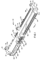
- an electrical connector generally designated 10, which includes an elongated dielectric housing, generally designated 12, adapted for mounting along an edge of a printed circuit board, as will be seen hereinafter.
- Housing 12 includes a front mating face 14 and a rear terminating face 16 and three mounting ears 18 project rearwardly of the terminating face for mounting to a top surface of the printed circuit board. Pins 19 project through ears 18 and into appropriate holes in the printed circuit board. Bottom surfaces 20 of mounting ears 18 engage the top surface of the board.
- connector 10 is adapted for mounting along an edge 44c ( Figure 3) of the printed circuit board.
- housing 12 includes a rear surface 22 for engaging the edge of the board.
- the rear surface 22 is coplanar with rear face 16.
- the housing is unitarily molded of dielectric material such as plastic or the like.
- electrical connector 10 is a combination connector which includes three sections spaced lengthwise of the connector and generally designated 24, 26 and 28.
- Section 24 will be termed the data section of the connector and includes a plurality of terminals 30 embodying the concepts of the invention.
- Section 26 will be termed the options section of the connector and includes a plurality of right-angled terminals 32 having pin portions 32a disposed in a center recessed area 34 in mating face 14 of housing 12 for mating with terminals of a complementary connecting device or mating connector (not shown).
- Section 28 will be termed the power section of the connector and includes four large formed terminals 36 located in an end recessed area 38 in mating face 14 of housing 12 for mating with the power terminals of the complementary mating connector.
- terminals 30 of data section 24 have mating portions (not visible in Figure 1) extending into terminal-receiving passages 40 in a "D-shaped" projecting portion 42 of housing 12 for insertion into a complementary D-shaped receptacle of the complementary connecting device.
- terminals 30 in data section 24 of connector 10 are arranged in pairs of upper and lower terminals, generally designated 30a and 30b, respectively, longitudinally along connector housing 12.
- One pair of the terminals 30a and 30b are removed from the housing in Figure 2 to facilitate the illustration thereof.
- the terminals are blanked terminals, i.e., blanked from sheet metal material rather than stamped and then formed into a shape out of the plane of the sheet metal material.
- the terminals in each pair also are quite clearly seen to be coplanar and are in that relationship when inserted into connector housing 12.
- connector 10 is shown to be mounted to a printed circuit board 44 having a top surface 44a and a bottom surface 44b.
- the bottom surface 20 of mounting ears 18 are shown engaged with top surface 44a of the printed circuit board, while rear surface 22 (i.e., rear terminating face 16) of connector housing 12 is in edge engagement or with an edge 44c of the printed circuit board.
- Bottom surface 20 of mounting ears 18 define the "seating plane" of connector 10 on circuit board 44.
- Terminal-receiving passages 40 can be seen clearly in Figure 3 to extend generally parallel to the seating plane, with the passages extending between the front mating face and the rear terminating face of connector housing 12.
- passages have front entry areas 40a of reduced size for receiving mating terminal pins of the complementary mating connector.
- the passages open into a recessed area 46 in terminating face 16 of the connector housing.
- passages 40 are arranged in pairs of upper and lower passages extending longitudinally along data section 24 of the connector, with the passages in each pair being in a plane perpendicular to the seating plane defined by bottom surface 20 of mounting ears 18.
- Upper and lower terminals 30a and 30b respectively, have substantially identical bifurcated mating portions 48 projecting from body portions 50 within their respective passages 40 toward entry areas 40a for mating with the terminal pins of the complementary mating connector.
- Body portions 50 of the terminals have barbs 52 for press fitting into the plastic material of housing 12 within passages 40.
- upper and lower terminals 30a and 30b respectively, have terminating portions 54 and 56, respectively, which have generally inverted U-shaped configurations. It can be seen in both Figures 2 and 3 that the U-shaped terminating portion 56 of lower terminal 30b is nested within the U-shaped terminating portion 54 of upper terminal 30a.
- U-shaped terminating portion 54 of upper terminal 30a defines an inner leg 58, an outer leg or tail 60 and a bridge portion 62 joining the legs.
- U-shaped terminating portion 56 of lower terminal 30b has an inner leg 64, an outer leg or tail 66 and a bridge portion 68 joining the legs.
- Inner legs 58 and 64 of the terminating portions of the upper and lower terminals may be located in recessed area 46 in rear terminating face 16 of connector housing 12.
- solder tails for the respective terminals.
- the solder tails project downwardly into holes 70 in printed circuit board 44 to ultimately be soldered to appropriate circuit traces in the holes.
- solder tails 60 and 66 may be increased or reduced and may extend significantly downward past lower barbs 52 of terminal 30b, as shown in phantom in Figure 4, so long as there is sufficient clearance between tips 60a and 66a of tails 60 and 66, respectively, and the top of bridge 62. This distance is affected by the length of web 84. This saves material during the blanking process of the terminals, as described hereinafter.
- a shoulder 72 is formed by a tab 74 projecting downwardly from the underside of bridge portion 62 of upper terminal 30a to define a means against which the terminal can be pushed or inserted into passages 40 in connector housing 12. Insertion forces are directed against upper terminal 30a as indicated by arrow "A” and against lower terminal 30b as indicated by arrow “B” to insert the terminals into the passages of the connector housing by a "stitching" type of insertion process. Therefore, insertion forces are not applied to the delicate tail portions 60 and 66 of the terminals, thereby avoiding the possibility of damaging or misaligning those small, fragile elements of the terminals.
- Figure 4 shows two pairs of terminals 30a and 30b as stamped from a blank of sheet metal material. It can be seen that terminals 30a still are joined to a carrier strip 80 by webs 82 which carry the terminals through the stamping operations. Terminal 30b of a first set of terminals is joined to terminal 30a of a second set of terminals by webs 84. Webs 82 and 84 eventually are severed so that the terminals can be stitched in pairs (see terminals 30a and 30b in Fig. 2) into passages 40 of connector housing 12 from rear terminating face 16 of the housing. Figure 4 shows how closely the terminals are located in the sheet of metal material during fabrication.
- This disposition of the terminals is afforded by nesting the U-shaped terminating portion 56 of the lower terminal within the U-shaped terminating portion 54 of the upper terminals. Material is saved by closely spacing the pairs of terminals. As seen clearly in Figure 4, the lower terminals 30b in each pair thereof are located quite closely to the upper terminals 30a of the next pair, joined only by small webs 84, to thereby minimize the amount of sheet metal material wasted between the pairs during blanking of the terminals.
Abstract
Description
- This invention generally relates to the art of electrical connectors and, particularly, to an electrical connector for mounting to a printed circuit board.
- A wide variety of electrical connectors are designed for mounting to printed circuit boards. Such connectors conventionally include a dielectric housing, such as a unitarily molded plastic housing, adapted for mounting to one side of the board. The housing typically includes a front mating face for mating with a complementary connecting device and a rear terminating face from which a plurality of terminals exit the housing for termination to circuit traces on the printed circuit board. The terminals normally include mating portions for mating with the terminals of the complementary connecting device, and terminating or tail portions projecting from the housing for interconnection, as by soldering, to circuit traces on the board or in holes in the board into which the tails are inserted.
- Some printed circuit board mounted electrical connectors are designed for mounting at an edge of the board. The connector housing has a mounting portion for mounting to a top surface of the board to define a seating plane for the connector. For instance, the main body portion of the connector housing may run along the edge of the board, with mounting ear portions of the housing projecting from the terminating face thereof for mounting to the top surface of the board. The tail portions of the terminals project from the housing, such as between the mounting ears projecting therefrom, for termination to the circuit traces on the board.
- Problems continue to arise in designing electrical connectors of the character described above. These problems often are associated with the design and/or assembly of the terminals in the connector housing. For instance, difficulties arise in inserting the terminals into the connector housing because of the delicate nature of the tail portions of the terminals projecting from the rear terminating face of the housing. These tail portions may be very thin elements and insertion forces would tend to bend or break the tail portions. Therefore, many such electrical connectors employ stamped and formed terminals which are formed with various portions to facilitate insertion of the terminals into the connector housing. On the other hand, it would be desirable to be able to simply blank the terminals from sheet metal material, but blanked terminals heretofore designed do not facilitate efficient insertion of the terminals into the connector housing.
- In addition, simple blanked terminals have a tendency to be relatively wasteful in the amount of sheet metal material required in the blanking process. The design of the terminals result in a considerable amount of sheet metal material going to waste after the terminals are fabricated.
- Still further, the configuration of the terminating/tail portions of the terminals which project from the housing for interconnection to circuit traces on the printed circuit board, have not been amenable to high density arrays. The terminating or tail portions of the terminals simply require too much space at the rear face of the connector housing.
- The present invention is directed to solving the various problems identified above and satisfying a need for a printed circuit board mounted electrical connector having an extremely compact terminal array which facilitates insertion of the terminals into the connector, the terminals being blanked of sheet metal material in a very efficient, nonwasteful configuration.
- An object, therefore, of the invention is to provide a new and improved circuit board mounted electrical connector of the character described above.
- In the exemplary embodiment of the invention, the electrical connector includes an elongated dielectric housing adapted for mounting along an edge of a printed circuit board with a mounting portion of the housing being mounted to a top surface of the board to define a seating plane for the connector. The housing has terminal-receiving passages extending generally parallel to the seating plane between a front mating face of the housing and a rear terminating face thereof. The passages are arranged in pairs of upper and lower passages longitudinally along at least a portion of the housing. The passages in each pair are in a plane perpendicular to the seating plane.
- A plurality of terminals are mounted in pairs on the housing, with mating portions in the passages and terminating portions projecting from the rear face of the housing for termination to circuit traces on the printed circuit board. The terminals are blanked from sheet metal material, with the terminals in each pair being coplanar. The terminating portions have generally inverted U-shaped configurations, with the U-shaped terminating portion of a lower terminal in each pair thereof being nested within the U-shaped terminating portion of an upper terminal in each pair thereof.
- The mounting portion of the housing may be located at a position for effectively locating the seating plane of the connector above the centerline of the lower passages in the pairs thereof.
- The U-shaped terminating portions of the terminals define an inner leg, an outer leg and a bridge portion of each terminating portion of each terminal. In the preferred embodiment of the invention, the inner legs are located in a recessed area in the rear terminating face of the housing. A shoulder is formed on the underside of each bridge portion of each upper terminal to facilitate insertion of the terminals into their respective passages. The outer legs form solder tails, with the tips of the solder tails being located in proximity to a plane defined by the bottom edge of the lower terminal.
- Other objects, features and advantages of the invention will be apparent from the following detailed description taken in connection with the accompanying drawings.
- The features of this invention which are believed to be novel are set forth with particularity in the appended claims. The invention, together with its objects and the advantages thereof, may be best understood by reference to the following description taken in conjunction with the accompanying drawings, in which like reference numerals identify like elements in the figures and in which:
- FIGURE 1 is a perspective view of an electrical connector embodying the concepts of the invention;
- FIGURE 2 is an enlarged perspective view of the right-hand end of the connector shown in Figure 1, with a pair of the terminals removed to facilitate an illustration thereof;
- FIGURE 3 is a vertical section, on an enlarged scale, taken generally along line 3-3 of Figure 1; and
- FIGURE 4 is a plan view of two pairs of terminals as blanked from a sheet of metal material, but with the terminals still joined to a carrier strip of the sheet.
- Referring to the drawings in greater detail, and first to Figure 1, the invention is embodied in an electrical connector, generally designated 10, which includes an elongated dielectric housing, generally designated 12, adapted for mounting along an edge of a printed circuit board, as will be seen hereinafter.
Housing 12 includes afront mating face 14 and a rear terminatingface 16 and threemounting ears 18 project rearwardly of the terminating face for mounting to a top surface of the printed circuit board. Pins 19 project throughears 18 and into appropriate holes in the printed circuit board.Bottom surfaces 20 ofmounting ears 18 engage the top surface of the board. In addition,connector 10 is adapted for mounting along anedge 44c (Figure 3) of the printed circuit board. To that end,housing 12 includes arear surface 22 for engaging the edge of the board. Therear surface 22 is coplanar withrear face 16. The housing is unitarily molded of dielectric material such as plastic or the like. - At this point, it should be understood that such terms as "top", "bottom", "upper" and "lower" are used herein to provide a clear and concise description of the invention as viewed in the drawings. However, the use of such terms herein and in the claims hereof are not intended in any way to be limiting, because it is known that printed circuit board mounted electrical connectors, as well as the printed circuit boards themselves, are omnidirectional in actual practice or use.
- Still referring to Figure 1,
electrical connector 10 is a combination connector which includes three sections spaced lengthwise of the connector and generally designated 24, 26 and 28.Section 24 will be termed the data section of the connector and includes a plurality ofterminals 30 embodying the concepts of the invention.Section 26 will be termed the options section of the connector and includes a plurality of right-angled terminals 32 havingpin portions 32a disposed in a center recessedarea 34 inmating face 14 ofhousing 12 for mating with terminals of a complementary connecting device or mating connector (not shown).Section 28 will be termed the power section of the connector and includes four large formedterminals 36 located in an end recessedarea 38 inmating face 14 ofhousing 12 for mating with the power terminals of the complementary mating connector. As will be described below,terminals 30 ofdata section 24 have mating portions (not visible in Figure 1) extending into terminal-receivingpassages 40 in a "D-shaped"projecting portion 42 ofhousing 12 for insertion into a complementary D-shaped receptacle of the complementary connecting device. - Referring to Figure 2 and as described in greater detail hereinafter,
terminals 30 indata section 24 ofconnector 10 are arranged in pairs of upper and lower terminals, generally designated 30a and 30b, respectively, longitudinally alongconnector housing 12. One pair of theterminals connector housing 12. - Referring to Figure 3 in conjunction with Figures 1 and 2,
connector 10 is shown to be mounted to a printedcircuit board 44 having atop surface 44a and abottom surface 44b. Thebottom surface 20 of mountingears 18 are shown engaged withtop surface 44a of the printed circuit board, while rear surface 22 (i.e., rear terminating face 16) ofconnector housing 12 is in edge engagement or with anedge 44c of the printed circuit board.Bottom surface 20 of mountingears 18 define the "seating plane" ofconnector 10 oncircuit board 44. Terminal-receivingpassages 40 can be seen clearly in Figure 3 to extend generally parallel to the seating plane, with the passages extending between the front mating face and the rear terminating face ofconnector housing 12. Actually, the passages havefront entry areas 40a of reduced size for receiving mating terminal pins of the complementary mating connector. The passages open into a recessedarea 46 in terminatingface 16 of the connector housing. Finally,passages 40 are arranged in pairs of upper and lower passages extending longitudinally alongdata section 24 of the connector, with the passages in each pair being in a plane perpendicular to the seating plane defined bybottom surface 20 of mountingears 18. - Upper and
lower terminals mating portions 48 projecting frombody portions 50 within theirrespective passages 40 towardentry areas 40a for mating with the terminal pins of the complementary mating connector.Body portions 50 of the terminals havebarbs 52 for press fitting into the plastic material ofhousing 12 withinpassages 40. - Generally, upper and
lower terminals portions portion 56 of lower terminal 30b is nested within theU-shaped terminating portion 54 ofupper terminal 30a. - U-shaped terminating
portion 54 ofupper terminal 30a defines aninner leg 58, an outer leg ortail 60 and abridge portion 62 joining the legs. U-shaped terminatingportion 56 of lower terminal 30b has aninner leg 64, an outer leg ortail 66 and abridge portion 68 joining the legs.Inner legs area 46 inrear terminating face 16 ofconnector housing 12. -
Outer legs portions lower terminals holes 70 in printedcircuit board 44 to ultimately be soldered to appropriate circuit traces in the holes. - In practice, the length of
solder tails lower barbs 52 ofterminal 30b, as shown in phantom in Figure 4, so long as there is sufficient clearance betweentips tails bridge 62. This distance is affected by the length ofweb 84. This saves material during the blanking process of the terminals, as described hereinafter. - A
shoulder 72 is formed by atab 74 projecting downwardly from the underside ofbridge portion 62 ofupper terminal 30a to define a means against which the terminal can be pushed or inserted intopassages 40 inconnector housing 12. Insertion forces are directed againstupper terminal 30a as indicated by arrow "A" and against lower terminal 30b as indicated by arrow "B" to insert the terminals into the passages of the connector housing by a "stitching" type of insertion process. Therefore, insertion forces are not applied to thedelicate tail portions - Lastly, Figure 4 shows two pairs of
terminals terminals 30a still are joined to acarrier strip 80 bywebs 82 which carry the terminals through the stamping operations. Terminal 30b of a first set of terminals is joined to terminal 30a of a second set of terminals bywebs 84.Webs terminals passages 40 ofconnector housing 12 fromrear terminating face 16 of the housing. Figure 4 shows how closely the terminals are located in the sheet of metal material during fabrication. This disposition of the terminals is afforded by nesting theU-shaped terminating portion 56 of the lower terminal within theU-shaped terminating portion 54 of the upper terminals. Material is saved by closely spacing the pairs of terminals. As seen clearly in Figure 4, thelower terminals 30b in each pair thereof are located quite closely to theupper terminals 30a of the next pair, joined only bysmall webs 84, to thereby minimize the amount of sheet metal material wasted between the pairs during blanking of the terminals. - It will be understood that the invention may be embodied in other specific forms without departing from the spirit or central characteristics thereof. The present examples and embodiments, therefore, are to be considered in all respects as illustrative and not restrictive, and the invention is not to be limited to the details given herein.
Claims (13)
- An electrical connector (10), comprising:
an elongated dielectric housing (12) adapted for mounting along an edge (44c) of a printed circuit board (44) with a mounting portion (18) of the housing being mounted to a top surface (44a) of the board to define a seating plane for the connector, the housing having terminal-receiving passages (40) extending generally parallel to said seating plane between a front mating face (14) of the housing and a rear terminating face (16) thereof, the passages being arranged in pairs of upper and lower passages longitudinally along at least a portion of the housing, with the passages in each pair being in a plane generally perpendicular to said seating plane; and
a plurality of terminals (30a, 30b) mounted in pairs on the housing (12) with mating portions (48) in said passages (40) and terminating portions (54, 56) projecting from the rear face of the housing for termination to circuit traces on the printed circuit board, the terminals being blanked from sheet metal material with the terminals in each pair being coplanar, the terminating portions (54, 56) having generally inverted U-shaped configurations with the U-shaped terminating portion (56) of a lower terminal (30b) in each pair thereof being nested within the U-shaped terminating portion (54) of an upper terminal (30a) in each pair thereof. - The electrical connector of claim 1 wherein said mounting portion (18) of the housing (12) is located at a position for effectively locating said seating plane above the centerline of the lower passages in said pairs thereof.
- The electrical connector of claim 2 wherein said inverted U-shaped terminating portions (54, 56) define an inner leg (58, 64), an outer leg (60, 66) and a bridge portion (62, 68) of each terminating portion of each terminal, and said inner legs (58, 64) are located in a recessed area (46) in the rear terminating face (16) of the housing (12).
- The electrical connector of claim 2 wherein said inverted U-shaped terminating portions (54, 56) define an inner leg (58, 64), an outer leg (60, 66) and a bridge portion (62, 68) of each terminating portion of each terminal, and including a shoulder (72) formed on the underside of the bridge portion (62) of each upper terminal (30a) to facilitate insertion of the terminals into their respective passages (40).
- The electrical connector of claim 2 wherein said inverted U-shaped terminating portions (54, 56) define an inner leg (58, 64), an outer leg (60, 66) and a bridge portion (62, 68) of each terminating portion of each terminal, the outer legs (60, 66) forming solder tails with the tips (60a, 66a) of the solder tails being located in proximity to a plane defined by the bottom edge (48) of the lower terminal (30b).
- The electrical connector of claim 1 wherein said inverted U-shaped terminating portions (54, 56) define an inner leg (58, 64), an outer leg (60, 66) and a bridge portion (62, 68) of each terminating portion of each terminal, and said inner legs (58, 64) are located in a recessed area (46) in the rear terminating face (16) of the housing (12).
- The electrical connector of claim 1 wherein said inverted U-shaped terminating portions (54, 56) define an inner leg (58, 64), an outer leg (60, 66) and a bridge portion (62, 68) of each terminating portion of each terminal, and including a shoulder (72) formed on the underside of the bridge portion (62) of each upper terminal (30a) to facilitate insertion of the terminals into their respective passages (40).
- The electrical connector of claim 1 wherein said inverted U-shaped terminating portions (54, 56) define an inner leg (58, 64), an outer leg (60, 66) and a bridge portion (62, 68) of each terminating portion of each terminal, the outer legs (60, 66) forming solder tails with the tips (60a, 66a) of the solder tails being located in proximity to a plane defined by the bottom edge (48) of the lower terminal (30b).
- An electrical connector (10), comprising:
an elongated dielectric housing (12) adapted for mounting to a surface (44a) of a printed circuit board (44) and including terminal-receiving passages (40) extending generally parallel to the board between a front mating face (14) of the housing and a rear terminating face (16) thereof, the passages (40) being arranged in pairs of upper and lower passages longitudinally along at least a portion of the housing, with the passages in each pair being in a plane generally perpendicular to the printed circuit board (44); and
a plurality of terminals (30a, 30b) mounted in pairs on the housing with mating portions (48) in said passages (40) and terminating portions (54, 56) projecting from the rear face (16) of the housing (12) for termination to circuit traces on the printed circuit board (44), the terminals being blanked from sheet metal material with the terminals in each pair being coplanar, the terminating portions (54, 56) having generally inverted U-shaped configurations with the U-shaped terminating portion (56) of a lower terminal (30b) in each pair thereof being nested within the U-shaped terminating portion (54) of an upper terminal (30a) in each pair thereof, said inverted U-shaped terminating portions defining an inner leg (58, 64), an outer leg (60, 66) and a bridge portion (62, 68) for each terminating portion of each terminal, and including a shoulder (72) formed on the underside of the bridge portion (62) of each upper terminal (30a) to facilitate insertion of the terminals into their respective passages (40). - The electrical connector of claim 9 wherein the outer legs (60, 66) of said U-shaped terminating portions (54, 56) form solder tails with the tips (60a, 66a) of the solder tails being located in proximity to a plane defined by the bottom edge (48) of the lower terminal (30b).
- The electrical connector of claim 9 wherein said inner legs (58, 64) of said inverted U-shaped terminating portions (54, 56) are located in a recessed area (46) in the rear terminating face (16) of the housing (12).
- An electrical connector (10), comprising:
an elongated dielectric housing (12) adapted for mounting to a surface (44a) of a printed circuit board (44) and including terminal-receiving passages (40) extending generally parallel to the board between a front mating face (14) of the housing and a rear terminating face (16) thereof, the passages (40) being arranged in pairs of upper and lower passages longitudinally along at least a portion of the housing, with the passages in each pair being in a plane generally perpendicular to the printed circuit board (44); and
a plurality of terminals (30a, 30b) mounted in pairs on the housing with mating portions (48) in said passages (40) and terminating portions (54, 56) projecting from the rear face (16) of the housing (12) for termination to circuit traces on the printed circuit board (44), the terminals being blanked from sheet metal material with the terminals in each pair being coplanar, the terminating portions (54, 56) having generally inverted U-shaped configurations with the U-shaped terminating portion (56) of a lower terminal (30b) in each pair thereof being nested within the U-shaped terminating portion (54) of an upper terminal (30a) in each pair thereof, said inverted U-shaped terminating portions defining an inner leg (58, 64), an outer leg (60, 66) and a bridge portion (62, 68) of each terminating portion of each terminal, the outer legs (60, 66) forming solder tails with the tips (60a, 66a) of the solder tails being located in proximity to a plane defined by the bottom edge (48) of the lower terminal (30b). - The electrical connector of claim 12 wherein said inner legs (58, 64) of said U-shaped terminating portions (54, 56) are located in a recessed area (46) in the rear terminating face (16) of the housing (12).
Applications Claiming Priority (2)
| Application Number | Priority Date | Filing Date | Title |
|---|---|---|---|
| US381614 | 1989-07-18 | ||
| US08/381,614 US5584709A (en) | 1995-01-30 | 1995-01-30 | Printed circuit board mounted electrical connector |
Publications (2)
| Publication Number | Publication Date |
|---|---|
| EP0724313A2 true EP0724313A2 (en) | 1996-07-31 |
| EP0724313A3 EP0724313A3 (en) | 1997-07-30 |
Family
ID=23505700
Family Applications (1)
| Application Number | Title | Priority Date | Filing Date |
|---|---|---|---|
| EP96100741A Withdrawn EP0724313A3 (en) | 1995-01-30 | 1996-01-19 | Printed circuit board mounted electrical connector |
Country Status (9)
| Country | Link |
|---|---|
| US (2) | US5584709A (en) |
| EP (1) | EP0724313A3 (en) |
| JP (2) | JP2704510B2 (en) |
| KR (1) | KR100208637B1 (en) |
| CN (1) | CN1051648C (en) |
| IN (1) | IN185689B (en) |
| MY (1) | MY121574A (en) |
| SG (1) | SG34382A1 (en) |
| TW (2) | TW385935U (en) |
Cited By (10)
| Publication number | Priority date | Publication date | Assignee | Title |
|---|---|---|---|---|
| EP0951102A2 (en) * | 1998-04-17 | 1999-10-20 | Berg Electronics Manufacturing B.V. | Power connector |
| EP1117154A1 (en) * | 2000-01-14 | 2001-07-18 | Siemens Aktiengesellschaft | Electrical connector with contacts fixable to housing |
| US6780027B2 (en) | 2003-01-28 | 2004-08-24 | Fci Americas Technology, Inc. | Power connector with vertical male AC power contacts |
| US6848950B2 (en) | 2003-05-23 | 2005-02-01 | Fci Americas Technology, Inc. | Multi-interface power contact and electrical connector including same |
| US6848953B2 (en) | 1998-04-17 | 2005-02-01 | Fci Americas Technology, Inc. | Power connector |
| US7037142B2 (en) | 2003-01-28 | 2006-05-02 | Fci Americas Technology, Inc. | Power connector with safety feature |
| US7314377B2 (en) | 1998-04-17 | 2008-01-01 | Fci Americas Technology, Inc. | Electrical power connector |
| USD619099S1 (en) | 2009-01-30 | 2010-07-06 | Fci Americas Technology, Inc. | Electrical connector |
| US8323049B2 (en) | 2009-01-30 | 2012-12-04 | Fci Americas Technology Llc | Electrical connector having power contacts |
| AT14207U1 (en) * | 2013-12-19 | 2015-06-15 | Tridonic Gmbh & Co Kg | Device for contacting electrical conductors and / or electrical contact elements, and light or electrical device |
Families Citing this family (52)
| Publication number | Priority date | Publication date | Assignee | Title |
|---|---|---|---|---|
| US5848903A (en) * | 1992-09-14 | 1998-12-15 | Melcher Ag | Flat pin connector for electronic circuit boards |
| US5848920A (en) * | 1996-07-16 | 1998-12-15 | Molex Incorporated | Fabrication of electrical terminals for edge card connectors |
| US6494734B1 (en) | 1997-09-30 | 2002-12-17 | Fci Americas Technology, Inc. | High density electrical connector assembly |
| US6431889B1 (en) * | 1997-12-23 | 2002-08-13 | Berg Technology, Inc. | High density edge card connector |
| TW356971U (en) * | 1998-03-09 | 1999-04-21 | Hon Hai Prec Ind Co Ltd | Electric connector with substrate secure apparatus |
| US6066815A (en) * | 1998-08-24 | 2000-05-23 | Illinois Tool Works Inc. | Electrical connector-power switch module |
| JP3456156B2 (en) | 1998-11-24 | 2003-10-14 | 住友電装株式会社 | Chain terminal |
| TW435846U (en) * | 1999-03-30 | 2001-05-16 | Hon Hai Prec Ind Co Ltd | Improved structure of electrical connector |
| JP4467099B2 (en) * | 1999-04-14 | 2010-05-26 | モレックス インコーポレイテド | Electrical connector terminals |
| SG97837A1 (en) | 2000-01-25 | 2003-08-20 | Molex Inc | Electrical connector with molded plastic housing |
| US6394823B1 (en) | 2000-05-26 | 2002-05-28 | Molex Incorporated | Connector with terminals having increased capacitance |
| TW488572U (en) * | 2000-05-30 | 2002-05-21 | Hon Hai Prec Ind Co Ltd | Transiting connector |
| KR200225814Y1 (en) * | 2000-12-26 | 2001-06-01 | 최윤식 | A connector |
| JP2003045519A (en) * | 2001-07-19 | 2003-02-14 | Molex Inc | Right-angle type electrical connector |
| US6492603B1 (en) | 2001-08-14 | 2002-12-10 | Illinois Tool Works Inc. | Power switch module |
| US6579107B1 (en) * | 2002-01-10 | 2003-06-17 | Osram Sylvania | Connector pin for an edge of a circuit board |
| US6814590B2 (en) * | 2002-05-23 | 2004-11-09 | Fci Americas Technology, Inc. | Electrical power connector |
| US6663420B1 (en) * | 2002-11-15 | 2003-12-16 | Hon Hai Precision Ind. Co., Ltd. | Adapter for exchanging data and transmitting power between PC and portable device |
| WO2005010163A2 (en) * | 2003-07-15 | 2005-02-03 | Barros Research Institute | Compositions and methods for immunotherapy of human immunotherapy of human immunodeficiency virus (hiv) |
| KR20060118567A (en) | 2003-12-31 | 2006-11-23 | 에프씨아이 | Electrical power contacts and connectors comprising same |
| US7384289B2 (en) | 2005-01-31 | 2008-06-10 | Fci Americas Technology, Inc. | Surface-mount connector |
| JP2006256448A (en) * | 2005-03-16 | 2006-09-28 | Tyco Electronics Amp Kk | Automobile connector assembly |
| US7493430B2 (en) * | 2005-07-14 | 2009-02-17 | Quantum Corporation | Data flow control and bridging architecture enhancing performance of removable data storage systems |
| KR100698542B1 (en) * | 2005-12-16 | 2007-03-21 | 한국몰렉스 주식회사 | Terminal's manufacturing method of dual card type connector of mobile phone |
| US20070155201A1 (en) * | 2006-01-05 | 2007-07-05 | Quantum Corporation, A Delaware Corporation | PCB edge connector |
| JP4832109B2 (en) * | 2006-02-27 | 2011-12-07 | 矢崎総業株式会社 | Electrical junction box |
| JP4833733B2 (en) * | 2006-05-18 | 2011-12-07 | 古河電気工業株式会社 | Wiring board unit |
| US7726982B2 (en) | 2006-06-15 | 2010-06-01 | Fci Americas Technology, Inc. | Electrical connectors with air-circulation features |
| US7779220B1 (en) | 2007-03-15 | 2010-08-17 | Quantum Corporation | Password-based media cartridge authentication |
| US7905731B2 (en) | 2007-05-21 | 2011-03-15 | Fci Americas Technology, Inc. | Electrical connector with stress-distribution features |
| US7762857B2 (en) * | 2007-10-01 | 2010-07-27 | Fci Americas Technology, Inc. | Power connectors with contact-retention features |
| US8062051B2 (en) | 2008-07-29 | 2011-11-22 | Fci Americas Technology Llc | Electrical communication system having latching and strain relief features |
| US8366485B2 (en) | 2009-03-19 | 2013-02-05 | Fci Americas Technology Llc | Electrical connector having ribbed ground plate |
| USD618181S1 (en) | 2009-04-03 | 2010-06-22 | Fci Americas Technology, Inc. | Asymmetrical electrical connector |
| USD618180S1 (en) | 2009-04-03 | 2010-06-22 | Fci Americas Technology, Inc. | Asymmetrical electrical connector |
| US8441786B2 (en) * | 2009-09-22 | 2013-05-14 | Jabil Circuit, Inc. | Electronic connectors and form factor adapters for electronic components |
| US8357009B2 (en) * | 2010-08-12 | 2013-01-22 | Tyco Electronics Corporation | Receptacle connector for mounting on a printed circuit |
| EP2624034A1 (en) | 2012-01-31 | 2013-08-07 | Fci | Dismountable optical coupling device |
| US8944831B2 (en) | 2012-04-13 | 2015-02-03 | Fci Americas Technology Llc | Electrical connector having ribbed ground plate with engagement members |
| US9257778B2 (en) | 2012-04-13 | 2016-02-09 | Fci Americas Technology | High speed electrical connector |
| USD727268S1 (en) | 2012-04-13 | 2015-04-21 | Fci Americas Technology Llc | Vertical electrical connector |
| USD718253S1 (en) | 2012-04-13 | 2014-11-25 | Fci Americas Technology Llc | Electrical cable connector |
| USD727852S1 (en) | 2012-04-13 | 2015-04-28 | Fci Americas Technology Llc | Ground shield for a right angle electrical connector |
| US9543703B2 (en) | 2012-07-11 | 2017-01-10 | Fci Americas Technology Llc | Electrical connector with reduced stack height |
| USD751507S1 (en) | 2012-07-11 | 2016-03-15 | Fci Americas Technology Llc | Electrical connector |
| USD745852S1 (en) | 2013-01-25 | 2015-12-22 | Fci Americas Technology Llc | Electrical connector |
| USD720698S1 (en) | 2013-03-15 | 2015-01-06 | Fci Americas Technology Llc | Electrical cable connector |
| DE102013012713A1 (en) * | 2013-08-01 | 2015-02-05 | Wieland Electric Gmbh | punching strips |
| US9246293B2 (en) * | 2013-10-31 | 2016-01-26 | Tyco Electronics Corporation | Leadframe for a contact module and method of manufacturing the same |
| US10553973B2 (en) * | 2015-09-08 | 2020-02-04 | Fci Usa Llc | Electrical power connector |
| TWI619320B (en) * | 2016-04-01 | 2018-03-21 | 慶良電子股份有限公司 | Method for forming embedded article, pre-structure prepared therefrom, and positioning scrap |
| JP6959876B2 (en) * | 2018-01-25 | 2021-11-05 | 日本航空電子工業株式会社 | connector |
Citations (6)
| Publication number | Priority date | Publication date | Assignee | Title |
|---|---|---|---|---|
| DE8811877U1 (en) * | 1988-09-19 | 1988-11-03 | Siemens Ag, 1000 Berlin Und 8000 Muenchen, De | |
| EP0365179A1 (en) * | 1988-10-17 | 1990-04-25 | The Whitaker Corporation | Electrical connector system |
| DE4040551A1 (en) * | 1989-12-20 | 1991-06-27 | Amp Inc | ELECTRICAL CONNECTOR ARRANGEMENT |
| EP0529350A2 (en) * | 1991-08-23 | 1993-03-03 | Molex Incorporated | Electrical connector for mounting on a printed circuit board |
| US5199886A (en) * | 1991-11-19 | 1993-04-06 | Amp Incorporated | Shrouded connector assembly |
| US5281165A (en) * | 1992-09-28 | 1994-01-25 | The Whitaker Corporation | Electrical connector shroud adapted for shorting bar removal |
Family Cites Families (10)
| Publication number | Priority date | Publication date | Assignee | Title |
|---|---|---|---|---|
| US4653837A (en) * | 1984-05-21 | 1987-03-31 | Stewart Stamping Corp. | Jack and connector |
| EP0177731A3 (en) * | 1984-09-26 | 1987-10-28 | Siemens Aktiengesellschaft | Plug-in electrical module |
| EP0203404B1 (en) * | 1985-05-31 | 1992-01-15 | Siemens Aktiengesellschaft | Device for connecting shielding hoods of multipolar plugs to the ground potential layer of a circuit board |
| US4722691A (en) * | 1986-02-03 | 1988-02-02 | General Motors Corporation | Header assembly for a printed circuit board |
| US4687267A (en) * | 1986-06-27 | 1987-08-18 | Amp Incorporated | Circuit board edge connector |
| ES2070283T3 (en) * | 1989-10-10 | 1995-06-01 | Whitaker Corp | CONTRAPLANE CONNECTOR WITH ADAPTED IMPEDANCES. |
| US5065236A (en) * | 1990-11-02 | 1991-11-12 | The United States Of America As Represented By The Administrator Of The National Aeronautics And Space Administration | Stereoscopic camera and viewing systems with undistorted depth presentation and reduced or eliminated erroneous acceleration and deceleration perceptions, or with perceptions produced or enhanced for special effects |
| US5112233A (en) * | 1991-05-30 | 1992-05-12 | Thomas & Betts Corporation | Electrical connector having contact retention means |
| GB9205087D0 (en) * | 1992-03-09 | 1992-04-22 | Amp Holland | Sheilded back plane connector |
| DE59404665D1 (en) * | 1993-09-24 | 1998-01-08 | Siemens Ag | Process for the production of contact element groups for plug connectors |
-
1995
- 1995-01-30 US US08/381,614 patent/US5584709A/en not_active Expired - Lifetime
- 1995-04-12 TW TW087216415U patent/TW385935U/en not_active IP Right Cessation
- 1995-04-12 TW TW087116461A patent/TW419866B/en not_active IP Right Cessation
- 1995-12-04 IN IN1565CA1995 patent/IN185689B/en unknown
-
1996
- 1996-01-19 JP JP8025809A patent/JP2704510B2/en not_active Expired - Fee Related
- 1996-01-19 EP EP96100741A patent/EP0724313A3/en not_active Withdrawn
- 1996-01-29 KR KR1019960001899A patent/KR100208637B1/en not_active IP Right Cessation
- 1996-01-29 CN CN96101217A patent/CN1051648C/en not_active Expired - Fee Related
- 1996-01-29 SG SG1996000527A patent/SG34382A1/en unknown
- 1996-01-29 MY MYPI96000326A patent/MY121574A/en unknown
- 1996-11-27 US US08/757,496 patent/US5782644A/en not_active Expired - Lifetime
-
1997
- 1997-03-14 JP JP1997002299U patent/JP3041845U/en not_active Expired - Lifetime
Patent Citations (6)
| Publication number | Priority date | Publication date | Assignee | Title |
|---|---|---|---|---|
| DE8811877U1 (en) * | 1988-09-19 | 1988-11-03 | Siemens Ag, 1000 Berlin Und 8000 Muenchen, De | |
| EP0365179A1 (en) * | 1988-10-17 | 1990-04-25 | The Whitaker Corporation | Electrical connector system |
| DE4040551A1 (en) * | 1989-12-20 | 1991-06-27 | Amp Inc | ELECTRICAL CONNECTOR ARRANGEMENT |
| EP0529350A2 (en) * | 1991-08-23 | 1993-03-03 | Molex Incorporated | Electrical connector for mounting on a printed circuit board |
| US5199886A (en) * | 1991-11-19 | 1993-04-06 | Amp Incorporated | Shrouded connector assembly |
| US5281165A (en) * | 1992-09-28 | 1994-01-25 | The Whitaker Corporation | Electrical connector shroud adapted for shorting bar removal |
Cited By (22)
| Publication number | Priority date | Publication date | Assignee | Title |
|---|---|---|---|---|
| US7374436B2 (en) | 1998-04-17 | 2008-05-20 | Fci Americas Technology, Inc. | Power connector |
| US6869294B2 (en) | 1998-04-17 | 2005-03-22 | Fci Americas Technology, Inc. | Power connector |
| US7070464B2 (en) | 1998-04-17 | 2006-07-04 | Fci Americas Technology, Inc. | Power connector |
| EP0951102A3 (en) * | 1998-04-17 | 2002-03-13 | Berg Electronics Manufacturing B.V. | Power connector |
| US7059919B2 (en) | 1998-04-17 | 2006-06-13 | Fci Americas Technology, Inc | Power connector |
| US8096814B2 (en) | 1998-04-17 | 2012-01-17 | Fci Americas Technology Llc | Power connector |
| US7488222B2 (en) | 1998-04-17 | 2009-02-10 | Fci Americas Technology, Inc. | Power connector |
| US6848953B2 (en) | 1998-04-17 | 2005-02-01 | Fci Americas Technology, Inc. | Power connector |
| EP0951102A2 (en) * | 1998-04-17 | 1999-10-20 | Berg Electronics Manufacturing B.V. | Power connector |
| US7314377B2 (en) | 1998-04-17 | 2008-01-01 | Fci Americas Technology, Inc. | Electrical power connector |
| US7309242B2 (en) | 1998-04-17 | 2007-12-18 | Fci Americas Technology, Inc. | Power connector |
| WO2001052358A1 (en) * | 2000-01-14 | 2001-07-19 | Siemens Aktiengesellschaft | Plug-in connection system comprising contact paths that can be fixed in an insulation body |
| EP1117154A1 (en) * | 2000-01-14 | 2001-07-18 | Siemens Aktiengesellschaft | Electrical connector with contacts fixable to housing |
| US6648696B2 (en) | 2000-01-14 | 2003-11-18 | Siemens Aktiengesellschaft | Plug-in connection system having contact paths fixed in an insulation body |
| US7037142B2 (en) | 2003-01-28 | 2006-05-02 | Fci Americas Technology, Inc. | Power connector with safety feature |
| US7140925B2 (en) | 2003-01-28 | 2006-11-28 | Fci Americas Technology, Inc. | Power connector with safety feature |
| USRE41283E1 (en) | 2003-01-28 | 2010-04-27 | Fci Americas Technology, Inc. | Power connector with safety feature |
| US6780027B2 (en) | 2003-01-28 | 2004-08-24 | Fci Americas Technology, Inc. | Power connector with vertical male AC power contacts |
| US6848950B2 (en) | 2003-05-23 | 2005-02-01 | Fci Americas Technology, Inc. | Multi-interface power contact and electrical connector including same |
| USD619099S1 (en) | 2009-01-30 | 2010-07-06 | Fci Americas Technology, Inc. | Electrical connector |
| US8323049B2 (en) | 2009-01-30 | 2012-12-04 | Fci Americas Technology Llc | Electrical connector having power contacts |
| AT14207U1 (en) * | 2013-12-19 | 2015-06-15 | Tridonic Gmbh & Co Kg | Device for contacting electrical conductors and / or electrical contact elements, and light or electrical device |
Also Published As
| Publication number | Publication date |
|---|---|
| CN1051648C (en) | 2000-04-19 |
| JP2704510B2 (en) | 1998-01-26 |
| SG34382A1 (en) | 1996-12-06 |
| CN1135666A (en) | 1996-11-13 |
| JPH08241771A (en) | 1996-09-17 |
| MY121574A (en) | 2006-02-28 |
| EP0724313A3 (en) | 1997-07-30 |
| TW385935U (en) | 2000-03-21 |
| US5584709A (en) | 1996-12-17 |
| IN185689B (en) | 2001-03-31 |
| JP3041845U (en) | 1997-10-03 |
| KR100208637B1 (en) | 1999-07-15 |
| KR960030496A (en) | 1996-08-17 |
| US5782644A (en) | 1998-07-21 |
| TW419866B (en) | 2001-01-21 |
Similar Documents
| Publication | Publication Date | Title |
|---|---|---|
| US5782644A (en) | Printed circuit board mounted electrical connector | |
| US4842528A (en) | Solder post retention means | |
| US5498167A (en) | Board to board electrical connectors | |
| JP2626868B2 (en) | Terminal of electrical connector and method of manufacturing the same | |
| US4655518A (en) | Backplane connector | |
| US5582519A (en) | Make-first-break-last ground connections | |
| EP0567007B1 (en) | Electrical connector for surface mouting | |
| US4275944A (en) | Miniature connector receptacles employing contacts with bowed tines and parallel mounting arms | |
| US4299436A (en) | Electrical connector | |
| US5192232A (en) | Electrical connector system utilizing thin male terminals | |
| US4880401A (en) | Electric female connector piece | |
| JPH0628791Y2 (en) | Terminal in electrical connector | |
| US4655522A (en) | Electrical terminal receptacle | |
| US20060121782A1 (en) | Electrical connector having an improved grounding path | |
| JPS61116782A (en) | Back board connector | |
| US5145383A (en) | Male electrical contact and connector embodying same | |
| EP0717468B1 (en) | Make-first-break-last ground connections | |
| KR970702596A (en) | Low Profile Electrical Connector | |
| EP0191539B1 (en) | Electrical connecting terminal for a connector | |
| EP0815621B1 (en) | Electrical receptacle assembly and spring contact therefor | |
| EP0639871A2 (en) | Surface mount electrical connector and terminal therefore | |
| US7086912B2 (en) | Electrical terminal having resistance against mating terminal removal | |
| GB2284947A (en) | Electrical socket connector | |
| EP0139786B1 (en) | Press fit connector insulator and contact | |
| JP3405943B2 (en) | connector |
Legal Events
| Date | Code | Title | Description |
|---|---|---|---|
| PUAI | Public reference made under article 153(3) epc to a published international application that has entered the european phase |
Free format text: ORIGINAL CODE: 0009012 |
|
| AK | Designated contracting states |
Kind code of ref document: A2 Designated state(s): DE ES FR GB IT NL |
|
| PUAL | Search report despatched |
Free format text: ORIGINAL CODE: 0009013 |
|
| AK | Designated contracting states |
Kind code of ref document: A3 Designated state(s): DE ES FR GB IT NL |
|
| 17P | Request for examination filed |
Effective date: 19980113 |
|
| 17Q | First examination report despatched |
Effective date: 20000120 |
|
| STAA | Information on the status of an ep patent application or granted ep patent |
Free format text: STATUS: THE APPLICATION IS DEEMED TO BE WITHDRAWN |
|
| 18D | Application deemed to be withdrawn |
Effective date: 20010821 |