EP0725301A1 - Active matrix liquid crystal display device with light shielding electrode connected to an independent potential - Google Patents
Active matrix liquid crystal display device with light shielding electrode connected to an independent potential Download PDFInfo
- Publication number
- EP0725301A1 EP0725301A1 EP96101363A EP96101363A EP0725301A1 EP 0725301 A1 EP0725301 A1 EP 0725301A1 EP 96101363 A EP96101363 A EP 96101363A EP 96101363 A EP96101363 A EP 96101363A EP 0725301 A1 EP0725301 A1 EP 0725301A1
- Authority
- EP
- European Patent Office
- Prior art keywords
- light shielding
- liquid crystal
- shielding film
- side conductive
- electrode
- Prior art date
- Legal status (The legal status is an assumption and is not a legal conclusion. Google has not performed a legal analysis and makes no representation as to the accuracy of the status listed.)
- Granted
Links
Images


Classifications
-
- G—PHYSICS
- G02—OPTICS
- G02F—OPTICAL DEVICES OR ARRANGEMENTS FOR THE CONTROL OF LIGHT BY MODIFICATION OF THE OPTICAL PROPERTIES OF THE MEDIA OF THE ELEMENTS INVOLVED THEREIN; NON-LINEAR OPTICS; FREQUENCY-CHANGING OF LIGHT; OPTICAL LOGIC ELEMENTS; OPTICAL ANALOGUE/DIGITAL CONVERTERS
- G02F1/00—Devices or arrangements for the control of the intensity, colour, phase, polarisation or direction of light arriving from an independent light source, e.g. switching, gating or modulating; Non-linear optics
- G02F1/01—Devices or arrangements for the control of the intensity, colour, phase, polarisation or direction of light arriving from an independent light source, e.g. switching, gating or modulating; Non-linear optics for the control of the intensity, phase, polarisation or colour
- G02F1/13—Devices or arrangements for the control of the intensity, colour, phase, polarisation or direction of light arriving from an independent light source, e.g. switching, gating or modulating; Non-linear optics for the control of the intensity, phase, polarisation or colour based on liquid crystals, e.g. single liquid crystal display cells
- G02F1/133—Constructional arrangements; Operation of liquid crystal cells; Circuit arrangements
- G02F1/136—Liquid crystal cells structurally associated with a semi-conducting layer or substrate, e.g. cells forming part of an integrated circuit
-
- G—PHYSICS
- G02—OPTICS
- G02F—OPTICAL DEVICES OR ARRANGEMENTS FOR THE CONTROL OF LIGHT BY MODIFICATION OF THE OPTICAL PROPERTIES OF THE MEDIA OF THE ELEMENTS INVOLVED THEREIN; NON-LINEAR OPTICS; FREQUENCY-CHANGING OF LIGHT; OPTICAL LOGIC ELEMENTS; OPTICAL ANALOGUE/DIGITAL CONVERTERS
- G02F1/00—Devices or arrangements for the control of the intensity, colour, phase, polarisation or direction of light arriving from an independent light source, e.g. switching, gating or modulating; Non-linear optics
- G02F1/01—Devices or arrangements for the control of the intensity, colour, phase, polarisation or direction of light arriving from an independent light source, e.g. switching, gating or modulating; Non-linear optics for the control of the intensity, phase, polarisation or colour
- G02F1/13—Devices or arrangements for the control of the intensity, colour, phase, polarisation or direction of light arriving from an independent light source, e.g. switching, gating or modulating; Non-linear optics for the control of the intensity, phase, polarisation or colour based on liquid crystals, e.g. single liquid crystal display cells
- G02F1/133—Constructional arrangements; Operation of liquid crystal cells; Circuit arrangements
- G02F1/1333—Constructional arrangements; Manufacturing methods
- G02F1/1335—Structural association of cells with optical devices, e.g. polarisers or reflectors
- G02F1/133509—Filters, e.g. light shielding masks
- G02F1/133512—Light shielding layers, e.g. black matrix
-
- G—PHYSICS
- G02—OPTICS
- G02F—OPTICAL DEVICES OR ARRANGEMENTS FOR THE CONTROL OF LIGHT BY MODIFICATION OF THE OPTICAL PROPERTIES OF THE MEDIA OF THE ELEMENTS INVOLVED THEREIN; NON-LINEAR OPTICS; FREQUENCY-CHANGING OF LIGHT; OPTICAL LOGIC ELEMENTS; OPTICAL ANALOGUE/DIGITAL CONVERTERS
- G02F1/00—Devices or arrangements for the control of the intensity, colour, phase, polarisation or direction of light arriving from an independent light source, e.g. switching, gating or modulating; Non-linear optics
- G02F1/01—Devices or arrangements for the control of the intensity, colour, phase, polarisation or direction of light arriving from an independent light source, e.g. switching, gating or modulating; Non-linear optics for the control of the intensity, phase, polarisation or colour
- G02F1/13—Devices or arrangements for the control of the intensity, colour, phase, polarisation or direction of light arriving from an independent light source, e.g. switching, gating or modulating; Non-linear optics for the control of the intensity, phase, polarisation or colour based on liquid crystals, e.g. single liquid crystal display cells
- G02F1/133—Constructional arrangements; Operation of liquid crystal cells; Circuit arrangements
- G02F1/1333—Constructional arrangements; Manufacturing methods
- G02F1/1337—Surface-induced orientation of the liquid crystal molecules, e.g. by alignment layers
- G02F1/133707—Structures for producing distorted electric fields, e.g. bumps, protrusions, recesses, slits in pixel electrodes
-
- G—PHYSICS
- G02—OPTICS
- G02F—OPTICAL DEVICES OR ARRANGEMENTS FOR THE CONTROL OF LIGHT BY MODIFICATION OF THE OPTICAL PROPERTIES OF THE MEDIA OF THE ELEMENTS INVOLVED THEREIN; NON-LINEAR OPTICS; FREQUENCY-CHANGING OF LIGHT; OPTICAL LOGIC ELEMENTS; OPTICAL ANALOGUE/DIGITAL CONVERTERS
- G02F1/00—Devices or arrangements for the control of the intensity, colour, phase, polarisation or direction of light arriving from an independent light source, e.g. switching, gating or modulating; Non-linear optics
- G02F1/01—Devices or arrangements for the control of the intensity, colour, phase, polarisation or direction of light arriving from an independent light source, e.g. switching, gating or modulating; Non-linear optics for the control of the intensity, phase, polarisation or colour
- G02F1/13—Devices or arrangements for the control of the intensity, colour, phase, polarisation or direction of light arriving from an independent light source, e.g. switching, gating or modulating; Non-linear optics for the control of the intensity, phase, polarisation or colour based on liquid crystals, e.g. single liquid crystal display cells
- G02F1/133—Constructional arrangements; Operation of liquid crystal cells; Circuit arrangements
- G02F1/136—Liquid crystal cells structurally associated with a semi-conducting layer or substrate, e.g. cells forming part of an integrated circuit
- G02F1/1362—Active matrix addressed cells
- G02F1/136213—Storage capacitors associated with the pixel electrode
-
- G—PHYSICS
- G02—OPTICS
- G02F—OPTICAL DEVICES OR ARRANGEMENTS FOR THE CONTROL OF LIGHT BY MODIFICATION OF THE OPTICAL PROPERTIES OF THE MEDIA OF THE ELEMENTS INVOLVED THEREIN; NON-LINEAR OPTICS; FREQUENCY-CHANGING OF LIGHT; OPTICAL LOGIC ELEMENTS; OPTICAL ANALOGUE/DIGITAL CONVERTERS
- G02F2201/00—Constructional arrangements not provided for in groups G02F1/00 - G02F7/00
- G02F2201/12—Constructional arrangements not provided for in groups G02F1/00 - G02F7/00 electrode
- G02F2201/128—Constructional arrangements not provided for in groups G02F1/00 - G02F7/00 electrode field shaping
Definitions
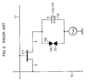
- FIG. 5 An equivalent circuit of one pixel in the prior art liquid crystal display device is shown in Fig. 5.
- the light shielding layer insulating film 114 and the gate insulating film 115 constitute a capacitor between the pixel electrode 5 and the light shielding film 116, and the same potential V com as for the light shielding film 116 is applied to the opposing electrode 121 which, together with the pixel electrode 105, sandwiches the liquid crystal 130.
- V sc a voltage about 15 to 25 V lower than V comopt (about 8 V)
- Fig. 14 shows the frequencies (number of pixels) of the standing disclination at the open portion in the pixel, and the number of pixels which are gathered from a sensory decision and in which the disclination having entered into the open portion in the pixel are present there without being extinguished.
- Fig. 15 is a sensory gathered diagram showing the area of the clear lines which do not move within the pixel but appear around the open portion of the pixel. These clear lines are generated uniformly in the entire pixels.
- the numeral 1 is for a gate electrode
- 2 is for a semiconductor film
- 3 is for a drain electrode
- 4 is for a source electrode
- 5 is for a pixel electrode
- 6 is for an open portion
- 7 is for an end of a TFT side conductive light shielding film
- 8 is for a TFT back channel side light shielding film contact portion
- 11 is for a scanning signal line
- 12 and 13 are for image signal lines
- 14 is for a back channel protective light shielding film.
- n + type amorphous silicon layer 119a (as shown, for example in Fig. 2 sectional view) at a region corresponding to the gate electrode 111 is removed.
- a nitride silicon film is deposited by a CVD process, and a passivation film 117 is formed.
Abstract
Description
- The present invention relates to a liquid crystal display device using an amorphous silicon thin film transistor (TFT), and more particularly to a high-definition liquid crystal display device having a conductive light shielding film at a transistor substrate side.
- A liquid crystal display device of the kind to which the present invention relates is proposed in, for example, Japanese Patent Application Kokai Publication No. Hei 3-50527. The proposal relates to a thin film transistor array substrate comprising a light shielding film provided on a glass substrate and having an open portion (an aperture) at a pixel electrode formation region, an interlayer insulating film provided on a surface including the light shielding film, a thin film transistor provided on the interlayer insulating film on the light shielding film, and a display electrode provided on the interlayer insulating film so as to be connected with the thin film transistor and be in alignment with the open portion. The light shielding of the TFT region other than the pixel electrode formation region is effected by the light shielding film provided on the glass substrate, and this light shielding suppresses an increase in the TFT off-current caused by back light irradiation, and shields the leakage light from outside the pixel electrode.
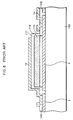
- The above prior art thin film transistor array substrate is shown in Figs. 1, 2 and 3, Fig. 1 being a plan view of a unit pixel, Fig. 2 being a sectional view taken along line 2-2 of Fig. 1, and Fig. 3 being a sectional view taken along line 3-3 in Fig. 1.
- In Fig. 1, the
numeral 1 is for a gate electrode, 2 is for a semiconductor layer, 3 is for a drain electrode, 4 is for a source electrode, 5 is for a pixel electrode, 7 is for an end of a TFT side conductive light shielding film, 6 is for an open portion, 11 is for a scanning signal line, and 12 and 13 are for image signal lines. The unit pixel is formed at a region surrounded by thescanning signal line 11 and theimage signal lines gate electrode 1 of the TFT and thescanning signal line 11, between the drain electrode and theimage signal line 12, and between thesource electrode 4 and thepixel electrode 5, and the conductive light shielding film having theopen portion 6 is provided at the pixel electrode formation region on the glass substrate. - The structure shown in Figs. 2 and 3 are formed by depositing a Cr film on a
glass substrate 100 by a sputtering process, and the portion of the Cr film that corresponds to the pixel electrode formation region is selectively etched so as to form an opening, thus forming thelight shielding film 116. Then, a nitride silicon film is deposited on a surface including thelight shielding film 116 by a CVD process, thus forming a light shieldinglayer insulating film 114. - Next, a Cr film is deposited on the light shielding
layer insulating film 114, and this is selectively etched so as to form agate electrode 111 on thelight shielding film 116. Thereafter, a nitride silicon film is deposited on a surface including thegate electrode 111 thereby forming agate insulating film 115. - On the gate
insulating film 115 corresponding to thegate electrode 111, there are selectively formed anamorphous silicon film 119 and an n+ typeamorphous silicon layer 119a provided on a surface of the amorphous silicon film and, on thegate insulating film 115 over an open portion of thelight shielding film 116, apixel electrode 105 is formed with the ITO film being selectively provided. Here, thepixel electrode 105 is provided so as to partly overlap peripheral portions of the opening of thelight shielding film 116. - Next, a Cr film is deposited on a surface including the
amorphous silicon film 119, and the resulting film is selectively etched whereby adrain electrode 113 and asource electrode 118 are formed. - Using the source/
drain electrodes amorphous silicon layer 119a at a region corresponding to thegate electrode 111 is etched away, thus forming a thin film transistor array substrate. In the arrangement shown in Fig. 4, thelight shielding film 116 and theopposing electrode 121 are of the same potential (=Vcom) so that the charging capacitor is formed between thelight shielding film 116 and thepixel electrode 105. - An equivalent circuit of one pixel in the prior art liquid crystal display device is shown in Fig. 5. The light shielding
layer insulating film 114 and thegate insulating film 115 constitute a capacitor between thepixel electrode 5 and thelight shielding film 116, and the same potential Vcom as for thelight shielding film 116 is applied to theopposing electrode 121 which, together with thepixel electrode 105, sandwiches theliquid crystal 130. - In the above prior art example, no light shielding film is disposed on the TFT back channel so that there is a problem with regard to light shielding characteristics.
- A thin film transistor array provided with a light shielding film on a back channel is disclosed, for example, in Japanese Patent Application Kokai Publication No. Sho 60-192370. In this example, a metal light shielding film on the back channel is coupled to either a first stage or a second stage of a gate line. A unit pixel of the thin film transistor array disclosed in the Japanese Patent Application Kokai Publication No. Sho 60-192370 is shown in a plan view in Fig. 6. Fig. 7 shows a sectional view taken along line 7-7 in Fig. 6, and Fig. 8 shows a sectional view taken along line 8-8 in Fig. 6.
- In Fig. 6, the
numeral 1 is for a gate line as a scanning signal line, 119 is for a semiconductor layer, 3 is for a drain electrode, 4 is for a source electrode, and 5 is for a pixel electrode. - In Figs. 7 and 8, the
numeral 100 is for a glass substrate, 1 is for a gate electrode, 3 is for a drain electrode, 4 is for a source electrode, 115 is for a gate insulating film, 144 is for a common electrode constituted by a transparent conductive layer, 145 is for an interlayer insulating film, 5 is for a pixel electrode, 117 is for a passivation insulating film, and 14 is for a conductive light shielding film on a TFT back channel. - As shown in Fig. 8, the conductive
light shielding film 14 of a metal such as Cr on the TFT back channel is connected to a firststage gate electrode 1. - A thin film transistor in which a light shielding film on a back channel is connected to either a source electrode or a drain electrode is disclosed, for example, in Japanese Utility Model Application Kokai Publication No. Hei 3-42124. In this example, as shown in Fig. 9, a back channel side conductive
light shielding film 14 formed of a metal is provided on apassivation insulating film 117 on a side opposite to thegate electrode 111 with a semiconductor layer of anamorphous silicon film 119 and/or an n+ typeamorphous silicon layer 119a being sandwiched therebetween, and the conductivelight shielding film 14 is electrically coupled to adrain electrode 3 of the TFT. - In these examples disclosed in the above Japanese Patent Application Kokai Publication No. Sho 60-192370 and Japanese Utility Model Application Kokai Publication No. Hei 3-42124, the back channel side light shielding film fulfills also a role of a back gate, but the potential thereof changes with time and, moreover, cannot be provided as desired or selectively.
- In each of the prior art liquid crystal display elements explained hereinabove, there is a trend that, when the element becomes highly defined, the lateral electric field between the pixel electrode and the TFT, the gate scanning line, and the image signal line, increases at the periphery of the pixel electrode (Fig. 4) and, as a consequence, the electric field which is expected to be in the vertical direction towards the liquid crystal between the pixel electrode and the opposing electrode is disturbed. For this reason, a disclination caused by a reverse tilt and a reverse twist of the liquid crystal is apt to occur around the pixel.
- The light is constantly transmitted at portions where a disclination occurs, thereby degrading the quality of display. Also, the disclination causes the open portions to move, and this is observed by the user as a residual image.
- An object of the invention, therefore, is to overcome the problems existing in the prior art, and to provide an active matrix type liquid crystal display device which is capable of suppressing the liquid crystal disclination that becomes a cause for coarse image appearance and residual image, and enhancing the quality of displayed image.
- According to one aspect of the invention, there is provided an active matrix type liquid crystal display device having a plurality of liquid crystal elements, each of the liquid crystal elements comprising:
a transistor section having a gate electrode, a gate insulating film, a semiconductor film, a source electrode, a drain electrode, and a passivation insulating film;
a transistor side conductive light shielding film (116) electrically coupled to the transistor section and having an open portion;
a pixel electrode formed over the open portion of the transistor side conductive light shielding film and electrically connected to the source electrode of the transistor section;
a liquid crystal layer formed on the passivation insulating film;
an opposing electrode formed on the liquid crystal layer; and
a means to apply to the transistor side conductive light shielding film a potential independent from a potential applied to the opposing electrode. - In the device according to the invention, an appropriate potential difference is provided, unlike in the prior art wherein the same potential is provided, between the opposing electrode and the transistor side conductive light shielding film so that, with respect to the vertical field components between the pixel electrode and the opposing electrode that are inherently required for the image display, the lateral field components around the pixel portion which become a cause for the reverse tilt of the liquid crystal are relatively reduced, thus reducing the disclination and providing excellent display characteristics without residual images.
- The above and other objects, features and advantages of the present invention will be apparent from the following description of preferred embodiments of the invention explained with reference to the accompanying drawings, in which:
- Fig. 1 is a plan view of a prior art unit pixel in a liquid crystal display device disclosed in Japanese Patent Application Kokai Publication No. Hei 3-50527;
- Fig. 2 is a sectional view of the prior art unit pixel, taken along line 2-2 in Fig. 1;
- Fig. 3 is a sectional view of the prior art unit pixel, taken along line 3-3 in Fig. 1;
- Fig. 4 is a sectional view of the prior art unit pixel for use in explaining the structure of the liquid crystal display element;
- Fig. 5 is an equivalent circuit diagram of the prior art unit pixel in Fig. 1;
- Fig. 6 is a plan view of a prior art unit pixel disclosed in Japanese Patent Application Kokai Publication No. Sho 60-192370;
- Fig. 7 is a sectional view of the prior art unit pixel, taken along line 7-7 in Fig. 6;
- Fig. 8 is a sectional view of the prior art unit pixel, taken along line 8-8 in Fig. 6;
- Fig. 9 is a sectional view of a prior art liquid crystal display element structure disclosed in Japanese Utility Model Application Kokai Publication No. Hei 3-42124;
- Fig. 10 is a sectional view of a unit pixel in a liquid crystal display device of a first embodiment according to the invention;
- Fig. 11 is an equivalent circuit diagram of the unit pixel of the first embodiment according to the invention;
- Fig. 12 is a diagram for showing locations of power supply terminals and a TFT side light shielding film layer in the structure of the first embodiment according to the invention;
- Fig. 13 is a diagram which is used for showing test results of the structure of the first embodiment and which shows the time periods in which the disclination was present in an open portion within the pixel;
- Fig. 14 is a diagram which is used for showing test results of the structure of the first embodiment and which shows the frequencies in which the disclination stands in the open portion within the pixel;
- Fig. 15 is a sensory gathered diagram for showing a clear line area observed around the pixel;
- Fig. 16 is a plan view of a unit pixel of a second embodiment according to the invention; and
- Fig. 17 is a sectional view of the unit pixel, taken along line 17-17 in Fig. 16.
- Now, preferred embodiments of the invention are explained with reference to the drawings. Throughout the explanation, the same or similar symbols and reference numerals are used for the same or similar elements. Where an element has been explained in describing the prior art, the same explanation is not repeated and only a difference therefrom is explained.
- A first embodiment of the invention is explained with reference to Figs. 10 - 15.
- In this embodiment, as shown in Fig. 10, a load voltage of potential Vsc is applied to a TFT side conductive
light shielding film 116, and an off-set voltage of potential Vcom is applied to the opposingelectrode 121. Thus, by the potential differences between thegate electrode 111 and thepixel electrode 105, and between thedrain electrode 113 and thepixel electrode 105, the vertical field components (B in Fig. 10) between thepixel electrode 105 and the opposing electrode 102 are relatively increased with respect to the lateral fields (A in Fig. 10) that are generated at the liquid crystal layer around the pixel, thus reducing the reverse tilt of the liquid crystal. - Fig. 11 shows an equivalent circuit of one pixel in this embodiment. As shown therein, there is a TFT side conductive
light shielding film 116 which, together with thepixel electrode 5, forms a capacitor by sandwiching between them agate insulating film 115 and a TFT light shieldinglayer insulating film 114. The potential Vsc is applied to the TFT side conductivelight shielding film 116 separately from a potential applied to the opposingelectrode 121. - The TFT side conductive
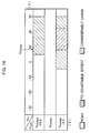
light shielding film 116 is, as shown in Fig. 12, a continuous flat plate. Power supply terminals are provided respectively at four corners, so that there is no lowering of the aperture efficiency caused by wiring of the power supply lines. - Test results, as examples, are shown in Figs. 13 - 15 which show the correlation of the voltage (Vsc) of the TFT side conductive
light shielding film 116 and the voltage (Vcom) of the opposingelectrode 121 with respect to the disclination. Fig. 13 shows periods of time in which the disclination exists in open portions within the pixels, Fig. 14 shows frequencies in which the disclination stands in the open portion within the pixel, and Fig. 15 shows, in a sensory gathered diagram, a clear line area observed around the pixel. In these figures, Vcomopt represents an opposing electrode voltage value at which flickering during the half-tone display becomes a minimum, that is, the DC component within the cell becomes a minimum. Normally, the opposing electrode voltage is set to the Vcomopt. - However, the Vcomopt value varies depending on the cell thickness, gate voltage and the drain voltage that are set, so that it is different depending on a panel. Thus, in this embodiment, the variations in the Vcomopt value of ±0.2 V are taken into account.
- Fig. 13 shows the time periods measured from the time when the pixel is changed from its white display to its black display to the time when the disclination extinguishes from within the open portion of the pixel.
- In the prior art devices, both the Vsc and the Vcom are set to Vcomopt, and it can be appreciated from the test data that the time period for the standing disclination within the pixel is longer. Also, as the Vcom is slightly lowered from Vcomopt, the time period for the standing disclination within the pixel becomes longer.
- In this embodiment, it can be appreciated that, by setting Vsc to a voltage about 15 to 25 V lower than Vcomopt (about 8 V), it is possible to suppress the entering of the disclination into the pixel.
- Fig. 14 shows the frequencies (number of pixels) of the standing disclination at the open portion in the pixel, and the number of pixels which are gathered from a sensory decision and in which the disclination having entered into the open portion in the pixel are present there without being extinguished.
- As seen in Fig. 14, when

- Fig. 15 is a sensory gathered diagram showing the area of the clear lines which do not move within the pixel but appear around the open portion of the pixel. These clear lines are generated uniformly in the entire pixels.
- It can be appreciated from Fig. 15 that, if the Vsc is changed when the Vcom is close to the Vcomopt, the clear line area becomes larger with an increase in |Vsc|. In this example, this is distinct when


- In this embodiment, when judged totally from the test results given in Figs. 13 - 15, it is considered that, when the Vsc is set to a level about 15 V to 20 V lower than the Vcomopt, the disclination is suppressed thus improving the display. Also, even when the Vcom is minutely deviated from the Vcomopt, the occurrence of the disclination is unlikely so that the quality of display is stabilized.
- Figs. 16 and 17 show a unit pixel in a liquid crystal display device of a second embodiment according to the invention, Fig. 16 showing a plan view thereof, and Fig. 17 showing a sectional view taken along line 17-17 in Fig. 16.
- In Fig. 16, the
numeral 1 is for a gate electrode, 2 is for a semiconductor film, 3 is for a drain electrode, 4 is for a source electrode, 5 is for a pixel electrode, 6 is for an open portion, 7 is for an end of a TFT side conductive light shielding film, 8 is for a TFT back channel side light shielding film contact portion, 11 is for a scanning signal line, 12 and 13 are for image signal lines, and 14 is for a back channel protective light shielding film. - As shown in Fig. 17, a Cr film is deposited on a
glass substrate 100 by a sputtering process, and an opening is formed by etching selectively the portion of the Cr film that corresponds to a display electrode formation region, whereby a TFT side conductivelight shielding film 116 is formed. Then, on the surface that includes the TFT side conductivelight shielding film 116, a nitride silicon film is deposited by a CVD process, thus forming a TFT light shieldinglayer insulating film 114. - After forming an opening by etching selectively the portion of the nitride silicon film that corresponds to a contact hole, a Cr film is deposited on the TFT light shielding
layer insulating film 114 whereby agate electrode 111 and agate contact 141 are formed. - A
gate insulating film 115 is formed by depositing a nitride silicon film by a CVD process. Thereafter, on thegate insulating film 115 corresponding to thegate electrode 111, anamorphous silicon film 119 and the n+ type amorphous silicon layer provided on a surface of the amorphous silicon film are selectively formed and, on thegate insulating film 115 on the open portion of thelight shielding film 116, an ITO film is selectively provided and thepixel electrode 105 is formed. Here, thepixel electrode 105 is formed so as to be partly overlapped by a periphery of the open portion of the TFT side conductivelight shielding film 116. - Next, the portion of the
gate insulating film 115 that corresponds to the contact hole is selectively etched. - A Cr film is deposited on the surface including the
amorphous silicon film 119, and this is selectively etched so as to form adrain electrode 113, a source electrode 118 (as shown, for example, in the Fig. 2 sectional view), and adrain contact 142. - Using source/
drain electrodes amorphous silicon layer 119a (as shown, for example in Fig. 2 sectional view) at a region corresponding to thegate electrode 111 is removed. - Next, a nitride silicon film is deposited by a CVD process, and a
passivation film 117 is formed. - Then, the portion corresponding to the contact hole is selectively etched. Subsequently, Cr is deposited on the
passivation film 117, and is selectively etched so as to form a TFT back channel side conductivelight shielding film 140, thus completing a thin film transistor array substrate of this embodiment. - The potential of the TFT back channel side conductive
light shielding film 140 becomes the same potential as that of the TFT side conductivelight shielding film 116 and can be set selectively as desired. Thus, the TFT back channel side conductivelight shielding film 140 functions as a stable back gate electrode. Unlike in the prior art, this back gate (numeral 14 in Fig. 16) is electrically independent from the gate line and the drain line, so that it is possible to provide thereto any desired potential stably. - When a minus voltage is applied to the back gate, it is possible to suppress, in addition to the disclination explained with respect to the first embodiment, the occurrence of the leakage current during the off-state of the TFT.
- While the invention has been described in its preferred embodiments, it is to be understood that the words which have been used are words of description rather than limitation and that changes within the purview of the appended claims may be made without departing from the true scope and spirit of the invention in its broader aspects.
Claims (4)
- An active matrix type liquid crystal display device having a plurality of liquid crystal elements, each of said liquid crystal elements characterized by comprising:
a transistor section having a gate electrode (1;111), a gate insulating film (115), a semiconductor film (2), a source electrode (4), a drain electrode (3;113), and a passivation insulating film (117);
a transistor side conductive light shielding film (116) electrically coupled to said transistor section and having an open portion;
a pixel electrode (5;105) formed over said open portion of said transistor side conductive light shielding film and electrically connected to said source electrode of said transistor section;
a liquid crystal layer (130) formed on said passivation insulating film;
an opposing electrode (121) formed on said liquid crystal layer; and
a means to apply to said transistor side conductive light shielding film a potential independent from a potential applied to said opposing electrode. - The active matrix type liquid crystal display device according to claim 1, in which said means to apply a potential comprises a first potential terminal (Vcom) connected to said opposing electrode (121) and a second potential terminal (Vsc) connected to said transistor side conductive light shielding film (116).
- The active matrix type liquid crystal display device according to claim 1, wherein said transistor side conductive light shielding film (116) is one to which is applied a load voltage several tens of volts lower than an off-set voltage applied to said opposing electrode (121).
- The active matrix type liquid crystal display device according to claim 3, which further comprises a back channel side conductive light shielding film (14;140) disposed on said passivation insulating film (117) on a back channel at said transistor section, and a contact hole provided in an insulating film layer (114,115,116) disposed on said transistor side conductive light shielding film (116), said back channel side conductive light shielding film and said transistor side conductive light shielding film being electrically interconnected through said contact hole.
Applications Claiming Priority (3)
| Application Number | Priority Date | Filing Date | Title |
|---|---|---|---|
| JP3623595 | 1995-01-31 | ||
| JP36235/95 | 1995-01-31 | ||
| JP3623595A JP2770763B2 (en) | 1995-01-31 | 1995-01-31 | Active matrix liquid crystal display |
Publications (2)
| Publication Number | Publication Date |
|---|---|
| EP0725301A1 true EP0725301A1 (en) | 1996-08-07 |
| EP0725301B1 EP0725301B1 (en) | 2003-04-02 |
Family
ID=12464121
Family Applications (1)
| Application Number | Title | Priority Date | Filing Date |
|---|---|---|---|
| EP96101363A Expired - Lifetime EP0725301B1 (en) | 1995-01-31 | 1996-01-31 | Active matrix liquid crystal display device with light shielding electrode connected to an independent potential |
Country Status (5)
| Country | Link |
|---|---|
| US (1) | US5859677A (en) |
| EP (1) | EP0725301B1 (en) |
| JP (1) | JP2770763B2 (en) |
| KR (1) | KR100221759B1 (en) |
| DE (1) | DE69627066T2 (en) |
Cited By (5)
| Publication number | Priority date | Publication date | Assignee | Title |
|---|---|---|---|---|
| EP0862077A2 (en) * | 1997-02-27 | 1998-09-02 | Seiko Epson Corporation | Liquid crystal device, manufacturing method thereof and projection type display device |
| US6297862B1 (en) * | 1996-10-16 | 2001-10-02 | Seiko Epson Corporation | Light shielding structure of a substrate for a liquid crystal device, liquid crystal device and projection type display device |
| US6862050B2 (en) | 1996-11-26 | 2005-03-01 | Samsung Electronics Co., Ltd. | Liquid crystal displays using organic insulating material for a gate insulating layer and/or having photolithographic formed spacers |
| US6940566B1 (en) | 1996-11-26 | 2005-09-06 | Samsung Electronics Co., Ltd. | Liquid crystal displays including organic passivation layer contacting a portion of the semiconductor layer between source and drain regions |
| US9705003B2 (en) | 2009-03-27 | 2017-07-11 | Semiconductor Energy Laboratory Co., Ltd. | Semiconductor device including first and second gate electrodes and stack of insulating layers |
Families Citing this family (21)
| Publication number | Priority date | Publication date | Assignee | Title |
|---|---|---|---|---|
| JP2937131B2 (en) * | 1996-08-30 | 1999-08-23 | 日本電気株式会社 | Liquid crystal display |
| US6088070A (en) * | 1997-01-17 | 2000-07-11 | Semiconductor Energy Laboratory Co., Ltd. | Active matrix liquid crystal with capacitor between light blocking film and pixel connecting electrode |
| JP3784491B2 (en) | 1997-03-28 | 2006-06-14 | 株式会社半導体エネルギー研究所 | Active matrix display device |
| JPH1152429A (en) * | 1997-06-05 | 1999-02-26 | Seiko Epson Corp | Substrate for liquid crystal panel, liquid crystal panel, and electronic equipment using the same |
| KR19990003712A (en) * | 1997-06-26 | 1999-01-15 | 김영환 | Ultra high aperture liquid crystal display device and manufacturing method thereof |
| JP3919900B2 (en) * | 1997-09-19 | 2007-05-30 | 株式会社半導体エネルギー研究所 | Liquid crystal display device and manufacturing method thereof |
| US6433841B1 (en) | 1997-12-19 | 2002-08-13 | Seiko Epson Corporation | Electro-optical apparatus having faces holding electro-optical material in between flattened by using concave recess, manufacturing method thereof, and electronic device using same |
| KR100325072B1 (en) | 1998-10-28 | 2002-08-24 | 주식회사 현대 디스플레이 테크놀로지 | Manufacturing method of high opening rate and high transmittance liquid crystal display device |
| KR20000027768A (en) | 1998-10-29 | 2000-05-15 | 김영환 | Lcd with high aperture rate and high transmissivity |
| JP3788259B2 (en) * | 2001-03-29 | 2006-06-21 | 株式会社日立製作所 | Liquid crystal display |
| JP2004118039A (en) | 2002-09-27 | 2004-04-15 | Seiko Epson Corp | Electro-optic apparatus and electronic appliance |
| TW583464B (en) * | 2002-11-12 | 2004-04-11 | Hannstar Display Corp | Liquid crystal display |
| KR101080356B1 (en) * | 2003-10-13 | 2011-11-04 | 삼성전자주식회사 | Thin film transistor, thin film transistor array panel, and display device |
| JP4882662B2 (en) * | 2006-01-12 | 2012-02-22 | セイコーエプソン株式会社 | Electro-optical device and electronic apparatus |
| CN102969361B (en) * | 2011-09-01 | 2015-09-23 | 中国科学院微电子研究所 | Light durability amorphous metal oxide TFT device and display device |
| KR102002858B1 (en) * | 2012-08-10 | 2019-10-02 | 삼성디스플레이 주식회사 | Thin-film transistor substrate and method of manufacturing the same |
| JP6098017B2 (en) * | 2014-02-17 | 2017-03-22 | エバーディスプレイ オプトロニクス(シャンハイ) リミテッド | Thin film transistor array substrate and manufacturing method thereof |
| KR20180070334A (en) * | 2016-12-16 | 2018-06-26 | 엘지디스플레이 주식회사 | Thin film transistor and display device including the same |
| JP6555304B2 (en) * | 2017-07-31 | 2019-08-07 | セイコーエプソン株式会社 | Liquid crystal display device and electronic device |
| JP6566079B1 (en) * | 2018-04-25 | 2019-08-28 | セイコーエプソン株式会社 | Electro-optical device, electronic equipment |
| CN112558364A (en) * | 2020-12-25 | 2021-03-26 | 深圳市华星光电半导体显示技术有限公司 | Display panel and display device thereof |
Citations (4)
| Publication number | Priority date | Publication date | Assignee | Title |
|---|---|---|---|---|
| EP0136509A2 (en) * | 1983-08-23 | 1985-04-10 | Kabushiki Kaisha Toshiba | Active matrix type display apparatus |
| JPS62143469A (en) * | 1985-12-18 | 1987-06-26 | Hitachi Ltd | Thin-film transistor |
| EP0556484A1 (en) * | 1991-12-25 | 1993-08-25 | Kabushiki Kaisha Toshiba | Liquid crystal display device |
| EP0592063A2 (en) * | 1992-09-14 | 1994-04-13 | Kabushiki Kaisha Toshiba | Active matrix liquid crystal display device |
Family Cites Families (9)
| Publication number | Priority date | Publication date | Assignee | Title |
|---|---|---|---|---|
| JPS60192370A (en) * | 1984-03-13 | 1985-09-30 | Seiko Instr & Electronics Ltd | Thin film transistor array |
| JPH0697317B2 (en) * | 1984-04-11 | 1994-11-30 | ホシデン株式会社 | Liquid crystal display |
| JPH0691252B2 (en) * | 1986-11-27 | 1994-11-14 | 日本電気株式会社 | Thin film transistor array |
| JPH0814669B2 (en) * | 1988-04-20 | 1996-02-14 | シャープ株式会社 | Matrix type display device |
| JPH0342124A (en) * | 1989-07-06 | 1991-02-22 | Akutoronikusu Kk | Method for forming long body to be meandrously bent |
| KR940004322B1 (en) * | 1991-09-05 | 1994-05-19 | 삼성전자 주식회사 | Liquid crystal display devices |
| JP2858499B2 (en) * | 1992-03-04 | 1999-02-17 | 日本電気株式会社 | Driving method of liquid crystal element |
| US5461501A (en) * | 1992-10-08 | 1995-10-24 | Hitachi, Ltd. | Liquid crystal substrate having 3 metal layers with slits offset to block light from reaching the substrate |
| US5657101A (en) * | 1995-12-15 | 1997-08-12 | Industrial Technology Research Institute | LCD having a thin film capacitor with two lower capacitor electrodes and a pixel electrode serving as an upper electrode |
-
1995
- 1995-01-31 JP JP3623595A patent/JP2770763B2/en not_active Expired - Lifetime
-
1996
- 1996-01-30 KR KR1019960002033A patent/KR100221759B1/en active IP Right Grant
- 1996-01-31 US US08/594,169 patent/US5859677A/en not_active Expired - Lifetime
- 1996-01-31 EP EP96101363A patent/EP0725301B1/en not_active Expired - Lifetime
- 1996-01-31 DE DE69627066T patent/DE69627066T2/en not_active Expired - Lifetime
Patent Citations (4)
| Publication number | Priority date | Publication date | Assignee | Title |
|---|---|---|---|---|
| EP0136509A2 (en) * | 1983-08-23 | 1985-04-10 | Kabushiki Kaisha Toshiba | Active matrix type display apparatus |
| JPS62143469A (en) * | 1985-12-18 | 1987-06-26 | Hitachi Ltd | Thin-film transistor |
| EP0556484A1 (en) * | 1991-12-25 | 1993-08-25 | Kabushiki Kaisha Toshiba | Liquid crystal display device |
| EP0592063A2 (en) * | 1992-09-14 | 1994-04-13 | Kabushiki Kaisha Toshiba | Active matrix liquid crystal display device |
Non-Patent Citations (1)
| Title |
|---|
| PATENT ABSTRACTS OF JAPAN vol. 11, no. 376 (E - 563) 8 December 1987 (1987-12-08) * |
Cited By (11)
| Publication number | Priority date | Publication date | Assignee | Title |
|---|---|---|---|---|
| US6297862B1 (en) * | 1996-10-16 | 2001-10-02 | Seiko Epson Corporation | Light shielding structure of a substrate for a liquid crystal device, liquid crystal device and projection type display device |
| US6388721B1 (en) | 1996-10-16 | 2002-05-14 | Seiko Epson Corporation | Light shielding structure of a substrate for a liquid crystal device, liquid crystal device and projection type display device |
| US6573955B2 (en) | 1996-10-16 | 2003-06-03 | Seiko Epson Corporation | Capacitance substrate for a liquid crystal device and a projection type display device |
| US6862050B2 (en) | 1996-11-26 | 2005-03-01 | Samsung Electronics Co., Ltd. | Liquid crystal displays using organic insulating material for a gate insulating layer and/or having photolithographic formed spacers |
| US6940566B1 (en) | 1996-11-26 | 2005-09-06 | Samsung Electronics Co., Ltd. | Liquid crystal displays including organic passivation layer contacting a portion of the semiconductor layer between source and drain regions |
| EP0862077A2 (en) * | 1997-02-27 | 1998-09-02 | Seiko Epson Corporation | Liquid crystal device, manufacturing method thereof and projection type display device |
| EP0862077A3 (en) * | 1997-02-27 | 1999-07-14 | Seiko Epson Corporation | Liquid crystal device, manufacturing method thereof and projection type display device |
| US6704068B2 (en) | 1997-02-27 | 2004-03-09 | Seiko Epson Corporation | LCD having a particular light-shield and connection |
| US6717633B2 (en) | 1997-02-27 | 2004-04-06 | Seiko Epson Corporatoin | Apparatus for providing light shielding in a liquid crystal display |
| CN100426107C (en) * | 1997-02-27 | 2008-10-15 | 精工爱普生株式会社 | Device comprising display region, liquid crystal apparatus and projecting display unit |
| US9705003B2 (en) | 2009-03-27 | 2017-07-11 | Semiconductor Energy Laboratory Co., Ltd. | Semiconductor device including first and second gate electrodes and stack of insulating layers |
Also Published As
| Publication number | Publication date |
|---|---|
| DE69627066T2 (en) | 2004-02-12 |
| KR960029868A (en) | 1996-08-17 |
| KR100221759B1 (en) | 1999-09-15 |
| JP2770763B2 (en) | 1998-07-02 |
| JPH08201773A (en) | 1996-08-09 |
| US5859677A (en) | 1999-01-12 |
| DE69627066D1 (en) | 2003-05-08 |
| EP0725301B1 (en) | 2003-04-02 |
Similar Documents
| Publication | Publication Date | Title |
|---|---|---|
| EP0725301B1 (en) | Active matrix liquid crystal display device with light shielding electrode connected to an independent potential | |
| EP0654828B1 (en) | TFT with reduced parasitic capacitance | |
| US7023502B2 (en) | Semiconductor device having light-shielded thin film transistor | |
| US7148506B2 (en) | Active matrix display and electrooptical device | |
| US5459595A (en) | Active matrix liquid crystal display | |
| US5694185A (en) | Matrix array of active matrix LCD and manufacturing method thereof | |
| US20060256270A1 (en) | Liquid crystal display device | |
| US8810757B2 (en) | Liquid crystal display device including a light-blocking member | |
| US7365825B2 (en) | Liquid crystal display device including repair pattern and method for fabricating the same | |
| US5796448A (en) | Structure for a parasitic capacitor and a storage capacitor in a thin film transistor-liquid crystal display and a method for making the same | |
| KR100474529B1 (en) | Reflective liquid crystal display device and its manufacturing method | |
| US20070024770A1 (en) | Liquid crystal display device and method of fabricating the same | |
| US6831295B2 (en) | TFT-LCD device having a reduced feed-through voltage | |
| US6717630B1 (en) | Liquid crystal display device and method of fabricating the same | |
| US7515215B2 (en) | Array substrate for liquid crystal display substrate having high aperture ratio and method for fabricating the same | |
| US5686976A (en) | Liquid crystal display with storage capacitors for holding electric charges | |
| US7687835B2 (en) | Liquid crystal display panel | |
| JP4030178B2 (en) | Active matrix display device | |
| JPH04100022A (en) | Liquid crystal display device and its driving method | |
| KR100828213B1 (en) | Apparatus for Thin Film Transistor Liquid Crystal Display and Method for Manufacturing the same | |
| JP2698503B2 (en) | Active matrix liquid crystal display | |
| JP2003280032A (en) | Liquid crystal display device | |
| JP2000267134A (en) | Active matrix type liquid crystal display device | |
| JPH05150269A (en) | Thin film transistor panel | |
| JPH10206868A (en) | Color liquid crystal display device |
Legal Events
| Date | Code | Title | Description |
|---|---|---|---|
| PUAI | Public reference made under article 153(3) epc to a published international application that has entered the european phase |
Free format text: ORIGINAL CODE: 0009012 |
|
| 17P | Request for examination filed |
Effective date: 19960508 |
|
| AK | Designated contracting states |
Kind code of ref document: A1 Designated state(s): DE FR GB |
|
| 17Q | First examination report despatched |
Effective date: 20010517 |
|
| GRAH | Despatch of communication of intention to grant a patent |
Free format text: ORIGINAL CODE: EPIDOS IGRA |
|
| GRAH | Despatch of communication of intention to grant a patent |
Free format text: ORIGINAL CODE: EPIDOS IGRA |
|
| GRAA | (expected) grant |
Free format text: ORIGINAL CODE: 0009210 |
|
| AK | Designated contracting states |
Designated state(s): DE FR GB |
|
| REG | Reference to a national code |
Ref country code: GB Ref legal event code: FG4D |
|
| REF | Corresponds to: |
Ref document number: 69627066 Country of ref document: DE Date of ref document: 20030508 Kind code of ref document: P |
|
| RAP2 | Party data changed (patent owner data changed or rights of a patent transferred) |
Owner name: NEC LCD TECHNOLOGIES, LTD. |
|
| REG | Reference to a national code |
Ref country code: GB Ref legal event code: 732E |
|
| ET | Fr: translation filed | ||
| PLBE | No opposition filed within time limit |
Free format text: ORIGINAL CODE: 0009261 |
|
| STAA | Information on the status of an ep patent application or granted ep patent |
Free format text: STATUS: NO OPPOSITION FILED WITHIN TIME LIMIT |
|
| 26N | No opposition filed |
Effective date: 20040105 |
|
| REG | Reference to a national code |
Ref country code: FR Ref legal event code: TP |
|
| REG | Reference to a national code |
Ref country code: GB Ref legal event code: 732E Free format text: REGISTERED BETWEEN 20100325 AND 20100331 |
|
| REG | Reference to a national code |
Ref country code: DE Ref legal event code: R082 Ref document number: 69627066 Country of ref document: DE Representative=s name: MURGITROYD & COMPANY, DE |
|
| REG | Reference to a national code |
Ref country code: FR Ref legal event code: TP Owner name: GOLD CHARM LIMITED, JP Effective date: 20130211 |
|
| REG | Reference to a national code |
Ref country code: DE Ref legal event code: R082 Ref document number: 69627066 Country of ref document: DE Representative=s name: MURGITROYD & COMPANY, DE Effective date: 20130321 Ref country code: DE Ref legal event code: R082 Ref document number: 69627066 Country of ref document: DE Representative=s name: MURGITROYD & COMPANY, DE Effective date: 20130305 Ref country code: DE Ref legal event code: R081 Ref document number: 69627066 Country of ref document: DE Owner name: GOLD CHARM LIMITED, WS Free format text: FORMER OWNER: NEC CORP., TOKYO, JP Effective date: 20130305 |
|
| REG | Reference to a national code |
Ref country code: FR Ref legal event code: PLFP Year of fee payment: 20 |
|
| PGFP | Annual fee paid to national office [announced via postgrant information from national office to epo] |
Ref country code: DE Payment date: 20150127 Year of fee payment: 20 |
|
| PGFP | Annual fee paid to national office [announced via postgrant information from national office to epo] |
Ref country code: GB Payment date: 20150128 Year of fee payment: 20 Ref country code: FR Payment date: 20150108 Year of fee payment: 20 |
|
| REG | Reference to a national code |
Ref country code: DE Ref legal event code: R071 Ref document number: 69627066 Country of ref document: DE |
|
| REG | Reference to a national code |
Ref country code: GB Ref legal event code: PE20 Expiry date: 20160130 |
|
| PG25 | Lapsed in a contracting state [announced via postgrant information from national office to epo] |
Ref country code: GB Free format text: LAPSE BECAUSE OF EXPIRATION OF PROTECTION Effective date: 20160130 |