EP0725430A2 - Method of manufacturing semiconductor device having capacitor - Google Patents
Method of manufacturing semiconductor device having capacitor Download PDFInfo
- Publication number
- EP0725430A2 EP0725430A2 EP96101154A EP96101154A EP0725430A2 EP 0725430 A2 EP0725430 A2 EP 0725430A2 EP 96101154 A EP96101154 A EP 96101154A EP 96101154 A EP96101154 A EP 96101154A EP 0725430 A2 EP0725430 A2 EP 0725430A2
- Authority
- EP
- European Patent Office
- Prior art keywords
- etching
- electrode film
- platinum
- dry
- film
- Prior art date
- Legal status (The legal status is an assumption and is not a legal conclusion. Google has not performed a legal analysis and makes no representation as to the accuracy of the status listed.)
- Granted
Links
Images

Classifications
-
- H—ELECTRICITY
- H01—ELECTRIC ELEMENTS
- H01L—SEMICONDUCTOR DEVICES NOT COVERED BY CLASS H10
- H01L21/00—Processes or apparatus adapted for the manufacture or treatment of semiconductor or solid state devices or of parts thereof
- H01L21/02—Manufacture or treatment of semiconductor devices or of parts thereof
- H01L21/02041—Cleaning
- H01L21/02057—Cleaning during device manufacture
- H01L21/02068—Cleaning during device manufacture during, before or after processing of conductive layers, e.g. polysilicon or amorphous silicon layers
- H01L21/02071—Cleaning during device manufacture during, before or after processing of conductive layers, e.g. polysilicon or amorphous silicon layers the processing being a delineation, e.g. RIE, of conductive layers
-
- H—ELECTRICITY
- H01—ELECTRIC ELEMENTS
- H01L—SEMICONDUCTOR DEVICES NOT COVERED BY CLASS H10
- H01L21/00—Processes or apparatus adapted for the manufacture or treatment of semiconductor or solid state devices or of parts thereof
- H01L21/02—Manufacture or treatment of semiconductor devices or of parts thereof
- H01L21/04—Manufacture or treatment of semiconductor devices or of parts thereof the devices having at least one potential-jump barrier or surface barrier, e.g. PN junction, depletion layer or carrier concentration layer
- H01L21/18—Manufacture or treatment of semiconductor devices or of parts thereof the devices having at least one potential-jump barrier or surface barrier, e.g. PN junction, depletion layer or carrier concentration layer the devices having semiconductor bodies comprising elements of Group IV of the Periodic System or AIIIBV compounds with or without impurities, e.g. doping materials
- H01L21/30—Treatment of semiconductor bodies using processes or apparatus not provided for in groups H01L21/20 - H01L21/26
- H01L21/31—Treatment of semiconductor bodies using processes or apparatus not provided for in groups H01L21/20 - H01L21/26 to form insulating layers thereon, e.g. for masking or by using photolithographic techniques; After treatment of these layers; Selection of materials for these layers
- H01L21/3205—Deposition of non-insulating-, e.g. conductive- or resistive-, layers on insulating layers; After-treatment of these layers
- H01L21/321—After treatment
- H01L21/3213—Physical or chemical etching of the layers, e.g. to produce a patterned layer from a pre-deposited extensive layer
- H01L21/32133—Physical or chemical etching of the layers, e.g. to produce a patterned layer from a pre-deposited extensive layer by chemical means only
- H01L21/32135—Physical or chemical etching of the layers, e.g. to produce a patterned layer from a pre-deposited extensive layer by chemical means only by vapour etching only
- H01L21/32136—Physical or chemical etching of the layers, e.g. to produce a patterned layer from a pre-deposited extensive layer by chemical means only by vapour etching only using plasmas
-
- H—ELECTRICITY
- H01—ELECTRIC ELEMENTS
- H01L—SEMICONDUCTOR DEVICES NOT COVERED BY CLASS H10
- H01L28/00—Passive two-terminal components without a potential-jump or surface barrier for integrated circuits; Details thereof; Multistep manufacturing processes therefor
- H01L28/40—Capacitors
- H01L28/60—Electrodes
- H01L28/65—Electrodes comprising a noble metal or a noble metal oxide, e.g. platinum (Pt), ruthenium (Ru), ruthenium dioxide (RuO2), iridium (Ir), iridium dioxide (IrO2)
Definitions
- the present invention relates to a method of manufacturing a semiconductor device having a capacitor using a high permittivity dielectric film or a ferroelectric film as a capacitor dielectric film, and in particular, to a method including a step of dry etching of the capacitor dielectric film.
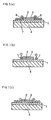
- FIG. 4(a), Fig. 4(b), Fig. 4(c), and Fig. 4(d) are sectional views for explaining the method of forming a capacitor included in a conventional semiconductor device.
- a platinum bottom electrode film 1 a dielectric film 2 comprised of a high permittivity dielectric film or a ferroelectric film, and a platinum top electrode film 3 are formed on a substrate 4 on which a silicon oxide film is deposited. Then, using a photoresist film 5 as mask, the platinum top electrode film 3 and the dielectric film 2 are dry-etched by using etching gas containing chlorine, and processed into a shape as shown in Fig. 4(b). Finally, by dry-etching the platinum bottom electrode film 1, a capacitor is formed.
- a defect 8 may be formed in a side wall 6 of the dielectric film 2 as shown in Fig. 4(c), or the side wall 6 is often degenerated into a difference substance 9 from the dielectric. When such state appears, short circuit of capacitor or increase of leakage current occurs, and the function as the capacitor is lost in an extreme case.
- the cause of appearance of such phenomenon may be considered as follows. On the side walls 6 of the platinum top electrode film 3 and the dielectric film 2 which are dry-etched, and on the surface 7 of the platinum bottom electrode film 1 which is exposed, atoms, ions or radicals of chlorine generated by decomposition of the etching gas due to discharge are massively deposited. These chlorine atoms, ions or radicals easily react with moisture to form an acidic aqueous solution, that is, hydrochloric acid.
- the side wall 6 of the dielectric film 2 composed of a dielectric oxide violently reacts with this hydrochloric acid, and the dielectric film 2 is eroded, or degenerated into other substance 9 different from the dielectric. As a result, it is considered to lead to short circuit of capacitor, increase of leakage current, or loss of function as capacitor.
- An object of the present invention is to provide a method of manufacturing a semiconductor device capable of preventing erosion of dielectric film, and suppressing occurrence of short circuit of capacitor and increase of leakage current.
- a method of manufacturing a semiconductor device comprises a step of forming a platinum bottom electrode film, a dielectric film, and a platinum top electrode film on a substrate on which circuit elements and wiring are formed, a step of dry-etching selectively the platinum top electrode film and the dielectric film by using etching gas containing at least one of chlorine, bromine and iodine, a step of irradiating plasma generated by discharging gas containing fluorine after the step of dry-etching, and a step of etching the platinum bottom electrode film.
- a method of manufacturing a semiconductor device comprises a step of forming a platinum bottom electrode film, a dielectric film, and a platinum top electrode film on a substrate on which circuit elements and wiring are formed, a step of dry-etching selectively the platinum top electrode film and the dielectric film by using etching gas containing at least one of chlorine, bromine and iodine, a step of heating the substrate after the step of dry-etching, and a step of etching the platinum bottom electrode film.
- decomposition products of the etching gas containing chlorine, bromine or iodine depositing on the side wall of the dielectric film or on the surface of the platinum bottom electrode film at the time of dry-etching are extremely decreased. It hence suppresses occurrence of defect or degeneration of the dielectric film which is induced by reacting the dielectric film with the acid formed by reaction of these decomposition products with moisture dielectric. Therefore occurrence of short circuit in capacitor and increase of leakage current may be extremely suppressed.
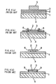
- Fig. 1(a), Fig. 1(b), and Fig. 1(c) are sectional views for explaining a method of forming a capacitor incorporated in a semiconductor device in a first embodiment of the invention.
- Fig. 2(a) and Fig. 2(b) are sectional views for explaining a method of forming a capacitor incorporated in a semiconductor device in a second embodiment of the invention.
- Fig. 3 is a comparative diagram of residual chlorine amount on the substrate in the first and second embodiments of the invention and a prior art.
- Fig. 4(a), Fig. 4(b), Fig. 4(c), and Fig. 4(d) are sectional views for explaining a conventional method of forming a capacitor incorporated in a semiconductor device.
- a platinum bottom electrode film 1, a dielectric film 2 composed of a high permittivity dielectric material or a ferroelectric material, and a platinum top electrode film 3 are formed on a substrate 4 on which circuit elements, wiring and an insulating film are formed.
- a photoresist film (not shown) as mask, the platinum top electrode film 3 and the dielectric film 2 are selectively dry-etched. Consequently, as shown in Fig. 1(b), plasma generated by discharging carbon tetrafluoride gas is irradiated to the substrate 4.
- the fluorine plasma obtained by discharge under the irradiating conditions of carbon tetrafluoride of 50 sccm, pressure of 1 Torr and RF power of 100 W load is irradiated for 30 seconds. Then the platinum bottom electrode film 1 is selectively dry-etched, and the capacitor are formed into a specified shape.
- CF 4 As the gas used in plasma irradiating, aside from the CF 4 above, it is preferred to use CHF 3 , NF 3 , XeF 2 , and SF 6 , and mixture of at least two of these gases.
- CF 4 and NF 3 gases are outstanding in the effects for preventing short circuit and suppressing increase of leakage current, and are hence preferred.
- the reason of suppression of occurrence of short circuit or increase of leakage current by plasma irradiating is not clearly explained yet. At least, however, from the results of measurement of residual chlorine concentration shown in Fig. 3, the following may be said.
- the residual chlorine concentration after plasma irradiating is expressed as a relative value in comparison with the residual chlorine concentration right after dry-etching by etching gas containing chlorine.
- the residual chlorine concentration after plasma irradiating corresponds to the irradiating conditions shown in the first embodiment.
- the residual chlorine concentration after plasma irradiating is decreased to about one-third of the residual chlorine concentration right after dry-etching.
- decomposition products such as chlorine atoms, ions and radicals formed by decomposition of the etching gas by discharge are massively deposited on the side walls 6 of the platinum top electrode film 3 and the dielectric film 2, and on the surface 7 of the platinum bottom electrode film 1 exposed by etching. Consequently, when the plasma generated by discharging the gas containing fluorine is irradiated, as shown in Fig. 1(b), the decomposition products are replaced by fluorine. In this case, since the chlorine is not strongly bonded with the platinum or dielectric on the side wall 6, the chlorine may be easily removed by irradiating an active fluorine plasma. Then, as shown in Fig. 1(c), the side wall 6 and the surface of the platinum bottom electrode film 1 are covered with fluorine.
- the role of the fluorine is not clarified. It is considered, among others, that the fluorine hardly reacts with moisture and hardly generates hydrofluoric acid, or hardly reacts with oxide dielectric, or reacts with oxide dielectric to form an inactive form on the surface which prevents reaction from propagating into the dielectric. Any way, the fluorine after plasma irradiating is considered to play a role in prevention of occurrence of defect or degeneration in the side wall of the dielectric film.
- Fig. 2(a) and Fig. 2(b) The second embodiment of the invention is described below by reference to Fig. 2(a) and Fig. 2(b).
- Fig. 2 (a) same as in the first embodiment, the platinum top electrode film 3 and the dielectric film 2 are dry-etched.
- Fig. 2(b) holding in nitrogen atmosphere same as the atmospheric pressure, the substrate is heated for 60 seconds at a temperature of 180 °C.
- the platinum bottom electrode film 1 is selectively dry-etched, and the capacitor is formed into a specified shape.
- heating atmosphere aside from the nitrogen gas, argon gas, helium gas or other inert gas may be used, or it may be also done in vacuum.
- the reason of effect caused by heating is estimated as follows from the results of measurement of residual chlorine concentration shown in Fig. 3.
- the residual chlorine concentration after heating process shown in Fig. 3 corresponds to the case of heating conditions shown in the second embodiment.
- the residual chlorine concentration after heating process is decreased to about one-third as compared with the residual chlorine concentration right after dry-etching.
- etching gas containing chlorine is used as etching gas, but the same effects as in the embodiments are obtained by using etching gas containing bromine or iodine, instead of chlorine, or etching gas containing two or more of chlorine, bromine and iodine. Therefore, all modified examples existing in the true spirit and scope of the invention are included in the scope of the claims.
Abstract
Description
- The present invention relates to a method of manufacturing a semiconductor device having a capacitor using a high permittivity dielectric film or a ferroelectric film as a capacitor dielectric film, and in particular, to a method including a step of dry etching of the capacitor dielectric film.
- Recently, efforts are concentrated on development of a microcomputer incorporating a capacitor using a high permittivity dielectric film or a ferroelectric film, being effective as measures for decreasing extraneous emission which is an electromagnetic noise, and a ferroelectric non-volatile RAM capable of operating at low voltage and writing/reading at high speed. Etching of these capacitor dielectric films has been done by wet etching as isotropic etching or non-selective ion milling. In these methods, however, high processing accuracy and high etching selectivity cannot be realized, and hence dry-etching technique is lately researched and developed intensively. The etching gas used in dry-etching of capacitor dielectric films and electrodes is halogen represented by chlorine or its compound. For example, chlorine alone, hydrogen chloride and carbon chloride have been reported.
- A conventional method of manufacturing a semiconductor device is described below by referring to drawings. Fig. 4(a), Fig. 4(b), Fig. 4(c), and Fig. 4(d) are sectional views for explaining the method of forming a capacitor included in a conventional semiconductor device.
- First, as shown in Fig. 4(a), a platinum
bottom electrode film 1, adielectric film 2 comprised of a high permittivity dielectric film or a ferroelectric film, and a platinumtop electrode film 3 are formed on asubstrate 4 on which a silicon oxide film is deposited. Then, using aphotoresist film 5 as mask, the platinumtop electrode film 3 and thedielectric film 2 are dry-etched by using etching gas containing chlorine, and processed into a shape as shown in Fig. 4(b). Finally, by dry-etching the platinumbottom electrode film 1, a capacitor is formed. - In this conventional manufacturing method, however, a
defect 8 may be formed in aside wall 6 of thedielectric film 2 as shown in Fig. 4(c), or theside wall 6 is often degenerated into adifference substance 9 from the dielectric. When such state appears, short circuit of capacitor or increase of leakage current occurs, and the function as the capacitor is lost in an extreme case. - The cause of appearance of such phenomenon may be considered as follows. On the
side walls 6 of the platinumtop electrode film 3 and thedielectric film 2 which are dry-etched, and on the surface 7 of the platinumbottom electrode film 1 which is exposed, atoms, ions or radicals of chlorine generated by decomposition of the etching gas due to discharge are massively deposited. These chlorine atoms, ions or radicals easily react with moisture to form an acidic aqueous solution, that is, hydrochloric acid. Theside wall 6 of thedielectric film 2 composed of a dielectric oxide violently reacts with this hydrochloric acid, and thedielectric film 2 is eroded, or degenerated intoother substance 9 different from the dielectric. As a result, it is considered to lead to short circuit of capacitor, increase of leakage current, or loss of function as capacitor. - This adsorption of moisture occurs always in operation in the manufacturing process of a semiconductor device such as exposure of substrate to the atmosphere or washing in water, and is hence inevitable. Such inconvenience is also noted when using bromine or iodine as etching gas.
- An object of the present invention is to provide a method of manufacturing a semiconductor device capable of preventing erosion of dielectric film, and suppressing occurrence of short circuit of capacitor and increase of leakage current.
- According to an aspect of the invention, a method of manufacturing a semiconductor device comprises a step of forming a platinum bottom electrode film, a dielectric film, and a platinum top electrode film on a substrate on which circuit elements and wiring are formed, a step of dry-etching selectively the platinum top electrode film and the dielectric film by using etching gas containing at least one of chlorine, bromine and iodine, a step of irradiating plasma generated by discharging gas containing fluorine after the step of dry-etching, and a step of etching the platinum bottom electrode film.
- According to other aspect of the invention, a method of manufacturing a semiconductor device comprises a step of forming a platinum bottom electrode film, a dielectric film, and a platinum top electrode film on a substrate on which circuit elements and wiring are formed, a step of dry-etching selectively the platinum top electrode film and the dielectric film by using etching gas containing at least one of chlorine, bromine and iodine, a step of heating the substrate after the step of dry-etching, and a step of etching the platinum bottom electrode film.
- By the plasma irradiating or heating process after dry-etching, decomposition products of the etching gas containing chlorine, bromine or iodine depositing on the side wall of the dielectric film or on the surface of the platinum bottom electrode film at the time of dry-etching are extremely decreased. It hence suppresses occurrence of defect or degeneration of the dielectric film which is induced by reacting the dielectric film with the acid formed by reaction of these decomposition products with moisture dielectric. Therefore occurrence of short circuit in capacitor and increase of leakage current may be extremely suppressed.
- Fig. 1(a), Fig. 1(b), and Fig. 1(c) are sectional views for explaining a method of forming a capacitor incorporated in a semiconductor device in a first embodiment of the invention.
- Fig. 2(a) and Fig. 2(b) are sectional views for explaining a method of forming a capacitor incorporated in a semiconductor device in a second embodiment of the invention.
- Fig. 3 is a comparative diagram of residual chlorine amount on the substrate in the first and second embodiments of the invention and a prior art.
- Fig. 4(a), Fig. 4(b), Fig. 4(c), and Fig. 4(d) are sectional views for explaining a conventional method of forming a capacitor incorporated in a semiconductor device.
- The first embodiment of the invention is described below while referring to Fig. 1(a), Fig. 1(b), and Fig. 1(c). Same parts as in the prior art shown in Fig. 4(a), Fig. 4(b), Fig. 4(c), and Fig. 4(d) are identified with same reference numerals.
- First, same as in the conventional method, a platinum
bottom electrode film 1, adielectric film 2 composed of a high permittivity dielectric material or a ferroelectric material, and a platinumtop electrode film 3 are formed on asubstrate 4 on which circuit elements, wiring and an insulating film are formed. Next, as shown in Fig. 1(a), using an etching gas containing chlorine, with a photoresist film (not shown) as mask, the platinumtop electrode film 3 and thedielectric film 2 are selectively dry-etched. Consequently, as shown in Fig. 1(b), plasma generated by discharging carbon tetrafluoride gas is irradiated to thesubstrate 4. At this time, the fluorine plasma obtained by discharge under the irradiating conditions of carbon tetrafluoride of 50 sccm, pressure of 1 Torr and RF power of 100 W load is irradiated for 30 seconds. Then the platinumbottom electrode film 1 is selectively dry-etched, and the capacitor are formed into a specified shape. - In thus manufactured semiconductor device, defect and degeneration in the
side wall 6 of the capacitor observed in the prior art were hardly noted. As a result of investigation into the rate of occurrence of short circuits in this semiconductor device, a short circuit was observed only in one out of 50 pieces, and the short circuit incidence was extremely decreased to about one-tenth or less of the prior art. Besides, increase of leakage current was not detected. - As the gas used in plasma irradiating, aside from the CF4 above, it is preferred to use CHF3, NF3, XeF2, and SF6, and mixture of at least two of these gases. In particular, CF4 and NF3 gases are outstanding in the effects for preventing short circuit and suppressing increase of leakage current, and are hence preferred.
- The reason of suppression of occurrence of short circuit or increase of leakage current by plasma irradiating is not clearly explained yet. At least, however, from the results of measurement of residual chlorine concentration shown in Fig. 3, the following may be said. In Fig. 3, incidentally, the residual chlorine concentration after plasma irradiating is expressed as a relative value in comparison with the residual chlorine concentration right after dry-etching by etching gas containing chlorine. The residual chlorine concentration after plasma irradiating corresponds to the irradiating conditions shown in the first embodiment. The residual chlorine concentration after plasma irradiating is decreased to about one-third of the residual chlorine concentration right after dry-etching.
- At the time of dry-etching by using etching gas containing chlorine, as shown in Fig. 1(a), decomposition products such as chlorine atoms, ions and radicals formed by decomposition of the etching gas by discharge are massively deposited on the
side walls 6 of the platinumtop electrode film 3 and thedielectric film 2, and on the surface 7 of the platinumbottom electrode film 1 exposed by etching. Consequently, when the plasma generated by discharging the gas containing fluorine is irradiated, as shown in Fig. 1(b), the decomposition products are replaced by fluorine. In this case, since the chlorine is not strongly bonded with the platinum or dielectric on theside wall 6, the chlorine may be easily removed by irradiating an active fluorine plasma. Then, as shown in Fig. 1(c), theside wall 6 and the surface of the platinumbottom electrode film 1 are covered with fluorine. - The role of the fluorine is not clarified. It is considered, among others, that the fluorine hardly reacts with moisture and hardly generates hydrofluoric acid, or hardly reacts with oxide dielectric, or reacts with oxide dielectric to form an inactive form on the surface which prevents reaction from propagating into the dielectric. Any way, the fluorine after plasma irradiating is considered to play a role in prevention of occurrence of defect or degeneration in the side wall of the dielectric film.
- The second embodiment of the invention is described below by reference to Fig. 2(a) and Fig. 2(b). First, as shown in Fig. 2 (a), same as in the first embodiment, the platinum
top electrode film 3 and thedielectric film 2 are dry-etched. Next, as shown in Fig. 2(b), holding in nitrogen atmosphere same as the atmospheric pressure, the substrate is heated for 60 seconds at a temperature of 180 °C. Afterwards, the platinumbottom electrode film 1 is selectively dry-etched, and the capacitor is formed into a specified shape. By this method of heating after dry-etching, too, nearly the same effects of prevention of occurrence of short circuit and suppression of increase of leakage current as in the first embodiment were obtained. - To obtain such prominent effects, it is preferred to heat at a temperature range from 150 °C to a temperature not to cause substantial change in the characteristics of the semiconductor device. More specifically, in an inert atmosphere, it is preferred to heat at a temperature between 150 °C and 450 °C. As heating atmosphere, aside from the nitrogen gas, argon gas, helium gas or other inert gas may be used, or it may be also done in vacuum.
- The reason of effect caused by heating is estimated as follows from the results of measurement of residual chlorine concentration shown in Fig. 3. The residual chlorine concentration after heating process shown in Fig. 3 corresponds to the case of heating conditions shown in the second embodiment. The residual chlorine concentration after heating process is decreased to about one-third as compared with the residual chlorine concentration right after dry-etching.
- As shown in Fig. 2(b), massive deposits of chlorine atoms, ions or radicals on the
side wall 6 or surface 7 of the platinumbottom electrode film 1 are easily detached by giving thermal energy to thesubstrate 4 because the chlorine is not strongly bonded with the platinum or dielectric on theside wall 6. Accordingly, the residual chlorine which reacts with moisture to produce hydrochloric acid is extremely decreased. Therefore, defect or degeneration of thedielectric film 2 hardly occurs, thereby suppressing formation of short circuit and increase of leakage current. - The invention is not limited to the illustrated embodiments alone, but may be modified in various forms. For example, in the foregoing embodiments, gas containing chlorine is used as etching gas, but the same effects as in the embodiments are obtained by using etching gas containing bromine or iodine, instead of chlorine, or etching gas containing two or more of chlorine, bromine and iodine. Therefore, all modified examples existing in the true spirit and scope of the invention are included in the scope of the claims.
Claims (7)
- A method of manufacturing a semiconductor device comprising:
a step of forming a platinum bottom electrode film, a dielectric film composed of a high permittivity dielectric material or a ferroelectric material, and a platinum top electrode film on a substrate on which circuit elements and wiring are formed;
a step of dry-etching selectively said platinum top electrode film and said dielectric film by using etching gas containing at least one of chlorine, bromine and iodine;
a step of irradiating plasma generated by discharging gas containing fluorine after said step of dry-etching; and
a step of etching said platinum bottom electrode film. - The method of claim 1, wherein said step of irradiating plasma is to replace decomposition products of said etching gas depositing on a side wall of said platinum top electrode film and said dielectric film and on a surface of said platinum bottom electrode film exposed by said step of dry-etching, with fluorine.
- The method of claim 1, wherein said gas containing fluorine is at least one of carbon tetrafluoride, methane trifluoride, nitrogen trifluoride, xenon fluoride and sulfur hexafluoride.
- A method of manufacturing a semiconductor device comprising:
a step of forming a platinum bottom electrode film, a dielectric film composed of a high permittivity dielectric material or a ferroelectric material, and a platinum top electrode film on a substrate on which circuit elements and wiring are formed;
a step of dry-etching selectively said platinum top electrode film and said dielectric film by using etching gas containing at least one of chlorine, bromine and iodine;
a step of heating said substrate after said step of dry-etching; and
a step of etching said platinum bottom electrode film. - The method of claim 4, wherein said heating step is done in a temperature range from 150 °C to a temperature not causing substantial change in the characteristics of said semiconductor device.
- The method of claim 4, wherein said heating step is done in a temperature range from 150 °C to 450 °C.
- The method of claim 4, wherein said heating step is done in an inert gas atmosphere or in vacuum.
Priority Applications (1)
| Application Number | Priority Date | Filing Date | Title |
|---|---|---|---|
| EP99106072A EP0932192B1 (en) | 1995-02-03 | 1996-01-27 | Etching of a platinum electrode and a dielectric or ferroelectric layer |
Applications Claiming Priority (3)
| Application Number | Priority Date | Filing Date | Title |
|---|---|---|---|
| JP7016829A JP2953974B2 (en) | 1995-02-03 | 1995-02-03 | Method for manufacturing semiconductor device |
| JP1682995 | 1995-02-03 | ||
| JP16829/95 | 1995-02-03 |
Related Child Applications (1)
| Application Number | Title | Priority Date | Filing Date |
|---|---|---|---|
| EP99106072A Division EP0932192B1 (en) | 1995-02-03 | 1996-01-27 | Etching of a platinum electrode and a dielectric or ferroelectric layer |
Publications (3)
| Publication Number | Publication Date |
|---|---|
| EP0725430A2 true EP0725430A2 (en) | 1996-08-07 |
| EP0725430A3 EP0725430A3 (en) | 1998-05-27 |
| EP0725430B1 EP0725430B1 (en) | 2001-07-11 |
Family
ID=11927088
Family Applications (2)
| Application Number | Title | Priority Date | Filing Date |
|---|---|---|---|
| EP99106072A Expired - Lifetime EP0932192B1 (en) | 1995-02-03 | 1996-01-27 | Etching of a platinum electrode and a dielectric or ferroelectric layer |
| EP96101154A Expired - Lifetime EP0725430B1 (en) | 1995-02-03 | 1996-01-27 | Method of manufacturing semiconductor device having capacitor |
Family Applications Before (1)
| Application Number | Title | Priority Date | Filing Date |
|---|---|---|---|
| EP99106072A Expired - Lifetime EP0932192B1 (en) | 1995-02-03 | 1996-01-27 | Etching of a platinum electrode and a dielectric or ferroelectric layer |
Country Status (6)
| Country | Link |
|---|---|
| US (1) | US5652171A (en) |
| EP (2) | EP0932192B1 (en) |
| JP (1) | JP2953974B2 (en) |
| KR (1) | KR0185489B1 (en) |
| CN (1) | CN1080926C (en) |
| DE (2) | DE69613723T2 (en) |
Cited By (11)
| Publication number | Priority date | Publication date | Assignee | Title |
|---|---|---|---|---|
| EP0795896A2 (en) * | 1996-03-15 | 1997-09-17 | ROHM Co., Ltd. | Dry etching method |
| EP0844652A1 (en) * | 1996-11-08 | 1998-05-27 | Siemens Aktiengesellschaft | Integratable capacitor, its fabrication method and memory array utilizing the capacitor |
| EP0867926A1 (en) * | 1997-03-25 | 1998-09-30 | Siemens Aktiengesellschaft | Capacitor electrode made of platinum metal |
| KR19980060614A (en) * | 1996-12-31 | 1998-10-07 | 김영환 | Manufacturing method of semiconductor device |
| WO1999036956A1 (en) * | 1998-01-13 | 1999-07-22 | Applied Materials, Inc. | Etching methods for anisotropic platinum profile |
| US6037264A (en) * | 1997-03-13 | 2000-03-14 | Applied Materials, Inc. | Method for removing redeposited veils from etched platinum |
| US6265318B1 (en) | 1998-01-13 | 2001-07-24 | Applied Materials, Inc. | Iridium etchant methods for anisotropic profile |
| US6323132B1 (en) | 1998-01-13 | 2001-11-27 | Applied Materials, Inc. | Etching methods for anisotropic platinum profile |
| EP1321977A1 (en) * | 2001-12-17 | 2003-06-25 | AMI Semiconductor Belgium BVBA | Method for reducing residual electric charge created by a previous process step on a conductive structure |
| EP1341218A2 (en) * | 2002-02-28 | 2003-09-03 | Fujitsu Limited | Semiconductor device manufacturing method |
| US6919168B2 (en) | 1998-01-13 | 2005-07-19 | Applied Materials, Inc. | Masking methods and etching sequences for patterning electrodes of high density RAM capacitors |
Families Citing this family (23)
| Publication number | Priority date | Publication date | Assignee | Title |
|---|---|---|---|---|
| JP3024747B2 (en) * | 1997-03-05 | 2000-03-21 | 日本電気株式会社 | Method for manufacturing semiconductor memory |
| US5846884A (en) * | 1997-06-20 | 1998-12-08 | Siemens Aktiengesellschaft | Methods for metal etching with reduced sidewall build up during integrated circuit manufacturing |
| KR100458293B1 (en) * | 1997-12-20 | 2005-02-05 | 주식회사 하이닉스반도체 | Post treatment method of metal interconnection of semiconductor device to avoid increase of resistance of aluminum metal interconnection and contact resistance |
| KR100333127B1 (en) * | 1998-06-29 | 2002-09-05 | 주식회사 하이닉스반도체 | Capacitor Manufacturing Method for Semiconductor Devices |
| US6204172B1 (en) | 1998-09-03 | 2001-03-20 | Micron Technology, Inc. | Low temperature deposition of barrier layers |
| US6323081B1 (en) | 1998-09-03 | 2001-11-27 | Micron Technology, Inc. | Diffusion barrier layers and methods of forming same |
| US7060584B1 (en) * | 1999-07-12 | 2006-06-13 | Zilog, Inc. | Process to improve high performance capacitor properties in integrated MOS technology |
| US6458648B1 (en) * | 1999-12-17 | 2002-10-01 | Agere Systems Guardian Corp. | Method for in-situ removal of side walls in MOM capacitor formation |
| KR100358149B1 (en) * | 2000-06-30 | 2002-10-25 | 주식회사 하이닉스반도체 | Method for forming FeRAM by using plasma treatment for recovering degradation of ferroelectric capacitor |
| US20020123008A1 (en) | 2000-12-21 | 2002-09-05 | Ning Xiang J. | Isotropic etch to form MIM capacitor top plates |
| US6444479B1 (en) * | 2001-04-18 | 2002-09-03 | Hynix Semiconductor Inc. | Method for forming capacitor of semiconductor device |
| JP4032916B2 (en) * | 2001-11-28 | 2008-01-16 | 三菱化学株式会社 | Etching solution |
| JP4865978B2 (en) * | 2002-02-28 | 2012-02-01 | 富士通セミコンダクター株式会社 | Manufacturing method of semiconductor device |
| JP4085094B2 (en) * | 2004-02-19 | 2008-04-30 | シャープ株式会社 | Manufacturing method of conductive element substrate, manufacturing method of liquid crystal display device |
| US7071117B2 (en) * | 2004-02-27 | 2006-07-04 | Micron Technology, Inc. | Semiconductor devices and methods for depositing a dielectric film |
| JP2006313833A (en) * | 2005-05-09 | 2006-11-16 | Seiko Epson Corp | Ferroelectric capacitor, method of forming the same and electronic device |
| US20060278339A1 (en) * | 2005-06-13 | 2006-12-14 | Lam Research Corporation, A Delaware Corporation | Etch rate uniformity using the independent movement of electrode pieces |
| JP2009266952A (en) * | 2008-04-23 | 2009-11-12 | Seiko Epson Corp | Method for manufacturing and manufacturing apparatus for device |
| JP2011119779A (en) * | 2011-03-22 | 2011-06-16 | Seiko Epson Corp | Method of forming ferroelectric capacitor, ferroelectric capacitor, and electronic device |
| CN102956430A (en) * | 2012-05-25 | 2013-03-06 | 深圳市华星光电技术有限公司 | Method for replacing helium atoms on film layer |
| US9224592B2 (en) * | 2013-09-12 | 2015-12-29 | Texas Intruments Incorporated | Method of etching ferroelectric capacitor stack |
| JP6210039B2 (en) * | 2014-09-24 | 2017-10-11 | セントラル硝子株式会社 | Deposit removal method and dry etching method |
| JP7199174B2 (en) * | 2018-07-26 | 2023-01-05 | 東京エレクトロン株式会社 | Etching method |
Citations (4)
| Publication number | Priority date | Publication date | Assignee | Title |
|---|---|---|---|---|
| GB2080737A (en) * | 1980-07-28 | 1982-02-10 | Fairchild Camera Instr Co | Plasma passivation of plasma-etched aluminium films |
| JPS593927A (en) * | 1982-06-29 | 1984-01-10 | Fujitsu Ltd | Etching of thin film |
| EP0122776A2 (en) * | 1983-04-13 | 1984-10-24 | Fujitsu Limited | Dry etching aluminum or aluminum alloy layer |
| EP0489179A1 (en) * | 1990-06-27 | 1992-06-10 | Fujitsu Limited | Method of manufacturing semiconductor integrated circuit and equipment for the manufacture |
Family Cites Families (11)
| Publication number | Priority date | Publication date | Assignee | Title |
|---|---|---|---|---|
| JPS61160939A (en) * | 1985-01-09 | 1986-07-21 | Nec Corp | Method of dry removal of si surface damage after dry etching |
| US4666555A (en) * | 1985-08-23 | 1987-05-19 | Intel Corporation | Plasma etching of silicon using fluorinated gas mixtures |
| US4847212A (en) * | 1987-01-12 | 1989-07-11 | Itt Gallium Arsenide Technology Center | Self-aligned gate FET process using undercut etch mask |
| JPH02151031A (en) * | 1988-12-02 | 1990-06-11 | Hitachi Ltd | Manufacture of semiconductor device |
| JPH03155621A (en) * | 1989-07-12 | 1991-07-03 | Toshiba Corp | Dry etching method |
| US5316572A (en) * | 1989-12-11 | 1994-05-31 | Nmb Ltd. | Method of manufacturing concrete for placement in air not requiring consolidation |
| JPH0467636A (en) * | 1990-07-06 | 1992-03-03 | Mitsubishi Electric Corp | Manufacture of semiconductor device |
| US5216572A (en) * | 1992-03-19 | 1993-06-01 | Ramtron International Corporation | Structure and method for increasing the dielectric constant of integrated ferroelectric capacitors |
| JPH0649667A (en) * | 1992-07-30 | 1994-02-22 | Sharp Corp | Dry etching method and its device |
| US5335138A (en) * | 1993-02-12 | 1994-08-02 | Micron Semiconductor, Inc. | High dielectric constant capacitor and method of manufacture |
| JP3460347B2 (en) * | 1994-03-30 | 2003-10-27 | 松下電器産業株式会社 | Method for manufacturing semiconductor device |
-
1995
- 1995-02-03 JP JP7016829A patent/JP2953974B2/en not_active Expired - Fee Related
-
1996
- 1996-01-27 EP EP99106072A patent/EP0932192B1/en not_active Expired - Lifetime
- 1996-01-27 DE DE69613723T patent/DE69613723T2/en not_active Expired - Lifetime
- 1996-01-27 EP EP96101154A patent/EP0725430B1/en not_active Expired - Lifetime
- 1996-01-27 DE DE69628677T patent/DE69628677T2/en not_active Expired - Lifetime
- 1996-01-31 US US08/594,945 patent/US5652171A/en not_active Expired - Lifetime
- 1996-02-02 CN CN96101296A patent/CN1080926C/en not_active Expired - Fee Related
- 1996-02-02 KR KR1019960002513A patent/KR0185489B1/en not_active IP Right Cessation
Patent Citations (4)
| Publication number | Priority date | Publication date | Assignee | Title |
|---|---|---|---|---|
| GB2080737A (en) * | 1980-07-28 | 1982-02-10 | Fairchild Camera Instr Co | Plasma passivation of plasma-etched aluminium films |
| JPS593927A (en) * | 1982-06-29 | 1984-01-10 | Fujitsu Ltd | Etching of thin film |
| EP0122776A2 (en) * | 1983-04-13 | 1984-10-24 | Fujitsu Limited | Dry etching aluminum or aluminum alloy layer |
| EP0489179A1 (en) * | 1990-06-27 | 1992-06-10 | Fujitsu Limited | Method of manufacturing semiconductor integrated circuit and equipment for the manufacture |
Non-Patent Citations (3)
| Title |
|---|
| PATENT ABSTRACTS OF JAPAN vol. 008, no. 081 (E-238), 13 April 1984 & JP 59 003927 A (FUJITSU KK), 10 January 1984, * |
| S. MAYUMI, Y. HATA, K. HUJIWARA, S. UEDA: "Post-treatments for reactive ion etching of Al-Si-Cu alloys" J. ELECTROCHEM. SOC. 137 (1990) 2534., XP000151176 * |
| SEIICHI YOKOYAMA ET AL: "HIGH TEMPERATURE ETCHING OF PZT/PT/TIN STRUCTURE BY HIGH DENSITY ECR PLASMA" INTERNATIONAL CONFERENCE ON SOLID STATE DEVICES AND MATERIALS, 23 August 1994, pages 721-723, XP000543969 * |
Cited By (19)
| Publication number | Priority date | Publication date | Assignee | Title |
|---|---|---|---|---|
| EP0795896A2 (en) * | 1996-03-15 | 1997-09-17 | ROHM Co., Ltd. | Dry etching method |
| EP0795896A3 (en) * | 1996-03-15 | 1999-06-02 | ROHM Co., Ltd. | Dry etching method |
| EP0844652A1 (en) * | 1996-11-08 | 1998-05-27 | Siemens Aktiengesellschaft | Integratable capacitor, its fabrication method and memory array utilizing the capacitor |
| KR19980060614A (en) * | 1996-12-31 | 1998-10-07 | 김영환 | Manufacturing method of semiconductor device |
| US6277762B1 (en) | 1997-03-13 | 2001-08-21 | Applied Materials, Inc. | Method for removing redeposited veils from etched platinum |
| US6037264A (en) * | 1997-03-13 | 2000-03-14 | Applied Materials, Inc. | Method for removing redeposited veils from etched platinum |
| US6087265A (en) * | 1997-03-13 | 2000-07-11 | Applied Materials, Inc. | Method for removing redeposited veils from etched platinum |
| EP0867926A1 (en) * | 1997-03-25 | 1998-09-30 | Siemens Aktiengesellschaft | Capacitor electrode made of platinum metal |
| US6265318B1 (en) | 1998-01-13 | 2001-07-24 | Applied Materials, Inc. | Iridium etchant methods for anisotropic profile |
| WO1999036956A1 (en) * | 1998-01-13 | 1999-07-22 | Applied Materials, Inc. | Etching methods for anisotropic platinum profile |
| US6323132B1 (en) | 1998-01-13 | 2001-11-27 | Applied Materials, Inc. | Etching methods for anisotropic platinum profile |
| US6482745B1 (en) | 1998-01-13 | 2002-11-19 | Applied Materials, Inc. | Etching methods for anisotropic platinum profile |
| US6749770B2 (en) | 1998-01-13 | 2004-06-15 | Jeng H. Hwang | Method of etching an anisotropic profile in platinum |
| US6777342B2 (en) | 1998-01-13 | 2004-08-17 | Jeng H. Hwang | Method of plasma etching platinum |
| US6919168B2 (en) | 1998-01-13 | 2005-07-19 | Applied Materials, Inc. | Masking methods and etching sequences for patterning electrodes of high density RAM capacitors |
| EP1321977A1 (en) * | 2001-12-17 | 2003-06-25 | AMI Semiconductor Belgium BVBA | Method for reducing residual electric charge created by a previous process step on a conductive structure |
| EP1341218A2 (en) * | 2002-02-28 | 2003-09-03 | Fujitsu Limited | Semiconductor device manufacturing method |
| EP1341218A3 (en) * | 2002-02-28 | 2004-08-11 | Fujitsu Limited | Semiconductor device manufacturing method |
| EP1592046A3 (en) * | 2002-02-28 | 2008-05-07 | Fujitsu Limited | Semiconductor device manufacturing method |
Also Published As
| Publication number | Publication date |
|---|---|
| KR0185489B1 (en) | 1999-04-15 |
| DE69628677T2 (en) | 2004-05-13 |
| JP2953974B2 (en) | 1999-09-27 |
| EP0932192A1 (en) | 1999-07-28 |
| EP0725430B1 (en) | 2001-07-11 |
| EP0932192B1 (en) | 2003-06-11 |
| DE69613723D1 (en) | 2001-08-16 |
| CN1080926C (en) | 2002-03-13 |
| CN1136218A (en) | 1996-11-20 |
| DE69628677D1 (en) | 2003-07-17 |
| JPH08213364A (en) | 1996-08-20 |
| EP0725430A3 (en) | 1998-05-27 |
| US5652171A (en) | 1997-07-29 |
| DE69613723T2 (en) | 2002-04-25 |
Similar Documents
| Publication | Publication Date | Title |
|---|---|---|
| US5652171A (en) | Method of manufacturing semiconductor device having capacitor | |
| US6254792B1 (en) | Isotropic dry cleaning process for noble metal integrated circuit structures | |
| US5685951A (en) | Methods and etchants for etching oxides of silicon with low selectivity in a vapor phase system | |
| US5716495A (en) | Cleaning method | |
| KR100230908B1 (en) | Semiconductor device making method | |
| US4734157A (en) | Selective and anisotropic dry etching | |
| US5624583A (en) | Method of manufacturing semiconductor device | |
| US5798303A (en) | Etching method for use in fabrication of semiconductor devices | |
| US5453156A (en) | Anisotropic polysilicon plasma etch using fluorine gases | |
| US5302241A (en) | Post etching treatment of semiconductor devices | |
| KR100269323B1 (en) | Method for etching platinum layer in semiconductor device | |
| JPH04120282A (en) | Method for etching film of al-based material | |
| Chow et al. | Plasma etching of sputtered Mo and MoSi2 thin films in NF3 gas mixtures | |
| JP3067737B2 (en) | Plasma etching method for vanadium oxide film | |
| JP2001358133A (en) | Method for performing anisotropic plasma etching using fluorochemical substance that is non- chlorofluorocarbon | |
| JPH06151387A (en) | Precision processing method of silicon | |
| Shibano et al. | Platinum etching in Ar/Cl 2 plasmas with a photoresist mask | |
| JPH0363209B2 (en) | ||
| JP3081200B2 (en) | Electronic device manufacturing method | |
| JP3440599B2 (en) | Via hole formation method | |
| US20010054599A1 (en) | Etching method | |
| JPH03248531A (en) | Etching method for silicon material to be etched | |
| JPH11340214A (en) | Manufacturing for semiconductor device | |
| JPH0444320A (en) | Dry etching | |
| JPH06104213A (en) | Manufacture of semiconductor device |
Legal Events
| Date | Code | Title | Description |
|---|---|---|---|
| PUAI | Public reference made under article 153(3) epc to a published international application that has entered the european phase |
Free format text: ORIGINAL CODE: 0009012 |
|
| AK | Designated contracting states |
Kind code of ref document: A2 Designated state(s): DE FR GB NL |
|
| PUAL | Search report despatched |
Free format text: ORIGINAL CODE: 0009013 |
|
| AK | Designated contracting states |
Kind code of ref document: A3 Designated state(s): DE FR GB NL |
|
| 17P | Request for examination filed |
Effective date: 19980827 |
|
| 17Q | First examination report despatched |
Effective date: 19981228 |
|
| GRAG | Despatch of communication of intention to grant |
Free format text: ORIGINAL CODE: EPIDOS AGRA |
|
| GRAG | Despatch of communication of intention to grant |
Free format text: ORIGINAL CODE: EPIDOS AGRA |
|
| GRAH | Despatch of communication of intention to grant a patent |
Free format text: ORIGINAL CODE: EPIDOS IGRA |
|
| GRAH | Despatch of communication of intention to grant a patent |
Free format text: ORIGINAL CODE: EPIDOS IGRA |
|
| GRAA | (expected) grant |
Free format text: ORIGINAL CODE: 0009210 |
|
| AK | Designated contracting states |
Kind code of ref document: B1 Designated state(s): DE FR GB NL |
|
| RAP2 | Party data changed (patent owner data changed or rights of a patent transferred) |
Owner name: MATSUSHITA ELECTRIC INDUSTRIAL CO., LTD. |
|
| REF | Corresponds to: |
Ref document number: 69613723 Country of ref document: DE Date of ref document: 20010816 |
|
| NLT2 | Nl: modifications (of names), taken from the european patent patent bulletin |
Owner name: MATSUSHITA ELECTRIC INDUSTRIAL CO., LTD. |
|
| ET | Fr: translation filed | ||
| REG | Reference to a national code |
Ref country code: GB Ref legal event code: IF02 |
|
| PLBE | No opposition filed within time limit |
Free format text: ORIGINAL CODE: 0009261 |
|
| STAA | Information on the status of an ep patent application or granted ep patent |
Free format text: STATUS: NO OPPOSITION FILED WITHIN TIME LIMIT |
|
| 26N | No opposition filed | ||
| REG | Reference to a national code |
Ref country code: FR Ref legal event code: TP |
|
| REG | Reference to a national code |
Ref country code: GB Ref legal event code: 746 Effective date: 20091215 |
|
| REG | Reference to a national code |
Ref country code: NL Ref legal event code: V1 Effective date: 20110801 |
|
| PG25 | Lapsed in a contracting state [announced via postgrant information from national office to epo] |
Ref country code: NL Free format text: LAPSE BECAUSE OF NON-PAYMENT OF DUE FEES Effective date: 20110801 |
|
| PGFP | Annual fee paid to national office [announced via postgrant information from national office to epo] |
Ref country code: FR Payment date: 20120202 Year of fee payment: 17 |
|
| PGFP | Annual fee paid to national office [announced via postgrant information from national office to epo] |
Ref country code: DE Payment date: 20120125 Year of fee payment: 17 |
|
| PGFP | Annual fee paid to national office [announced via postgrant information from national office to epo] |
Ref country code: GB Payment date: 20120125 Year of fee payment: 17 |
|
| GBPC | Gb: european patent ceased through non-payment of renewal fee |
Effective date: 20130127 |
|
| REG | Reference to a national code |
Ref country code: FR Ref legal event code: ST Effective date: 20130930 |
|
| PG25 | Lapsed in a contracting state [announced via postgrant information from national office to epo] |
Ref country code: DE Free format text: LAPSE BECAUSE OF NON-PAYMENT OF DUE FEES Effective date: 20130801 |
|
| REG | Reference to a national code |
Ref country code: DE Ref legal event code: R119 Ref document number: 69613723 Country of ref document: DE Effective date: 20130801 |
|
| PG25 | Lapsed in a contracting state [announced via postgrant information from national office to epo] |
Ref country code: FR Free format text: LAPSE BECAUSE OF NON-PAYMENT OF DUE FEES Effective date: 20130131 Ref country code: GB Free format text: LAPSE BECAUSE OF NON-PAYMENT OF DUE FEES Effective date: 20130127 |
|
| PGFP | Annual fee paid to national office [announced via postgrant information from national office to epo] |
Ref country code: NL Payment date: 20100131 Year of fee payment: 15 |