EP0729206A2 - PCMCIA input/output card connector - Google Patents
PCMCIA input/output card connector Download PDFInfo
- Publication number
- EP0729206A2 EP0729206A2 EP96300459A EP96300459A EP0729206A2 EP 0729206 A2 EP0729206 A2 EP 0729206A2 EP 96300459 A EP96300459 A EP 96300459A EP 96300459 A EP96300459 A EP 96300459A EP 0729206 A2 EP0729206 A2 EP 0729206A2
- Authority
- EP
- European Patent Office
- Prior art keywords
- terminals
- housing
- connector
- spline
- shield
- Prior art date
- Legal status (The legal status is an assumption and is not a legal conclusion. Google has not performed a legal analysis and makes no representation as to the accuracy of the status listed.)
- Granted
Links
Images


Classifications
-
- H—ELECTRICITY
- H01—ELECTRIC ELEMENTS
- H01R—ELECTRICALLY-CONDUCTIVE CONNECTIONS; STRUCTURAL ASSOCIATIONS OF A PLURALITY OF MUTUALLY-INSULATED ELECTRICAL CONNECTING ELEMENTS; COUPLING DEVICES; CURRENT COLLECTORS
- H01R12/00—Structural associations of a plurality of mutually-insulated electrical connecting elements, specially adapted for printed circuits, e.g. printed circuit boards [PCB], flat or ribbon cables, or like generally planar structures, e.g. terminal strips, terminal blocks; Coupling devices specially adapted for printed circuits, flat or ribbon cables, or like generally planar structures; Terminals specially adapted for contact with, or insertion into, printed circuits, flat or ribbon cables, or like generally planar structures
- H01R12/70—Coupling devices
- H01R12/71—Coupling devices for rigid printing circuits or like structures
- H01R12/72—Coupling devices for rigid printing circuits or like structures coupling with the edge of the rigid printed circuits or like structures
- H01R12/722—Coupling devices for rigid printing circuits or like structures coupling with the edge of the rigid printed circuits or like structures coupling devices mounted on the edge of the printed circuits
- H01R12/725—Coupling devices for rigid printing circuits or like structures coupling with the edge of the rigid printed circuits or like structures coupling devices mounted on the edge of the printed circuits containing contact members presenting a contact carrying strip, e.g. edge-like strip
-
- H—ELECTRICITY
- H01—ELECTRIC ELEMENTS
- H01R—ELECTRICALLY-CONDUCTIVE CONNECTIONS; STRUCTURAL ASSOCIATIONS OF A PLURALITY OF MUTUALLY-INSULATED ELECTRICAL CONNECTING ELEMENTS; COUPLING DEVICES; CURRENT COLLECTORS
- H01R13/00—Details of coupling devices of the kinds covered by groups H01R12/70 or H01R24/00 - H01R33/00
- H01R13/40—Securing contact members in or to a base or case; Insulating of contact members
- H01R13/405—Securing in non-demountable manner, e.g. moulding, riveting
-
- H—ELECTRICITY
- H01—ELECTRIC ELEMENTS
- H01R—ELECTRICALLY-CONDUCTIVE CONNECTIONS; STRUCTURAL ASSOCIATIONS OF A PLURALITY OF MUTUALLY-INSULATED ELECTRICAL CONNECTING ELEMENTS; COUPLING DEVICES; CURRENT COLLECTORS
- H01R13/00—Details of coupling devices of the kinds covered by groups H01R12/70 or H01R24/00 - H01R33/00
- H01R13/648—Protective earth or shield arrangements on coupling devices, e.g. anti-static shielding
- H01R13/658—High frequency shielding arrangements, e.g. against EMI [Electro-Magnetic Interference] or EMP [Electro-Magnetic Pulse]
- H01R13/6581—Shield structure
- H01R13/6582—Shield structure with resilient means for engaging mating connector
-
- H—ELECTRICITY
- H01—ELECTRIC ELEMENTS
- H01R—ELECTRICALLY-CONDUCTIVE CONNECTIONS; STRUCTURAL ASSOCIATIONS OF A PLURALITY OF MUTUALLY-INSULATED ELECTRICAL CONNECTING ELEMENTS; COUPLING DEVICES; CURRENT COLLECTORS
- H01R13/00—Details of coupling devices of the kinds covered by groups H01R12/70 or H01R24/00 - H01R33/00
- H01R13/648—Protective earth or shield arrangements on coupling devices, e.g. anti-static shielding
- H01R13/658—High frequency shielding arrangements, e.g. against EMI [Electro-Magnetic Interference] or EMP [Electro-Magnetic Pulse]
- H01R13/6591—Specific features or arrangements of connection of shield to conductive members
- H01R13/6594—Specific features or arrangements of connection of shield to conductive members the shield being mounted on a PCB and connected to conductive members
- H01R13/6595—Specific features or arrangements of connection of shield to conductive members the shield being mounted on a PCB and connected to conductive members with separate members fixing the shield to the PCB
Definitions
- This invention is related to electrical connectors for providing an interface between a printed circuit card and an external device or component. More specifically, this invention is related to an input/output electrical connector which can be used with a PC Card, such as a PCMCIA card assembly. Still more specifically, this invention is related to an input output electrical connector or header that complies with the PCMCIA Open System Standard for I/O Connectors and can be used as a local area network connector, a modem simple implementation connector, or a modem multifunctional connector.
- PCMCIA Personal Computer Memory Card International Association
- PCMCIA is an organization composed of a number of manufacturers of PC cards and related peripheral equipment. This organization has established standards or specifications for memory cards used with computers and especially for use with laptop, notebook or portable computers. PC cards which meet this PCMCIA standard are credit card-sized wafers. The dimensions of a PCMCIA standard card assembly are 85 mm. in length and 55 mm. wide. These cards employ a high density electrical connector to connect the PC card to the personal computer or other computing equipment with which the PCMCIA card is to be used. This high density electrical connector includes a number of sockets which mate with pins on the computer. This high density connector meets the requirements of PC Card standard, Release 2.0, PCMCIA (September 1991) which defines the PC Card's physical outline and the connector system qualification test parameters, including reliability, durability and environmental test parameters.
- PCMCIA cards can be used with laptop or notebook personal computers to provide an interface to a peripheral device such as an external floppy disk drive.
- PCMCIA cards can also be used as memory cards, including Flash, EPROM, DRAM or as other memory cards. When used in these applications the PCMCIA cards are inserted into a card slot and into engagement with a standard high density connector mounted on a printed circuit board in the computer.
- PCMCIA cards are not limited to use as memory cards or external floppy disk drives that have no external connection other than their connection to the computer. These cards can also be used as part of an external modem which is connected to an external telephone line or as part of a local area network interface assembly. Modems and local area networks in turn require specific cable interconnections. For example, a modem will typically require an RJ-11 six position connector for an interface to a standard telephone line. Different local area networks typically require different connections. These local area network interconnections include RJ-45 eight position connectors for shielded or unshielded twisted pair, coaxial connections for Ethernet and fiber optic connections for FDDI local area networks.
- PCMCIA Card Standard Release 2.0 defines an Open System Standard including a common male and female I/O interface.
- This Open System Standard includes three distinct mating key configurations. One key is for local area network applications including Ethernet, Token Ring, Arcnet, Fast Ethernet and ATM. A second key configuration is for Modem Simple Implementation. A third key configuration is for Modem Multifunctional.
- These Open System mating interface key configurations are formed on a keyed housing spline which comprises a generally flat protruding blade on the insulative housing of the Card I/O connector mounted on the PCMCIA card assembly.
- Pin terminals are located side by side on the opposite surface of the keyed spline. These standard connectors include up to fifteen pins spaced apart on 0.80 mm centerlines. Pins 1 and 15 are make first, break last contacts having a length of 3.9 mm. Pins 2-14 are signal contacts have a length of 3.0 mm. The front ends of the longer make first, break last contacts on the ends of the terminal array are closer to the forward edge of the keyed connector spline than the signal contacts. Therefore, the make first, break last contacts will engage corresponding contacts of the standard cable connector while the signal contacts are disengaged to prevent extraneous signals or excessive signal levels from being transmitted on pins 2-14.
- the Open System Standard defining the I/O configuration is intended to promote availability of multi-sourced I/O connectors satisfying PCMCIA-mandated design criteria by promoting uniform implementation interfaces. However, there is no requirement that all I/O connectors meet this standard. Nonstandard I/O connectors will function properly provided that compatible male and female configurations are used. There are a number of prior configurations which predate the Open System Standards.
- U.S. Patent 5,330,360 discloses a memory card frame kit which uses an I/O connector that does not employ the keying configuration mandated by the PCMCIA Open System Standard. That connector includes an array of pin terminals located on one side of a housing spline, but does not employ tongue and groove keys on the opposite spline surface.
- That connector also employs an insulative housing with a D-shaped mating interface.
- a keying rib extends between the D-shaped peripheral mating interface and the centrally positioned spline on commercially available configurations of this connector.
- Other commercially available versions of I/O connectors include a mating interface in which the outer periphery is defined by a shield with distinct housing keys located on the sides of the mating interface.
- Versions of these connectors manufactured by AMP Incorporated employ insert molded housings in which the terminals are held in position in a mold by molding pins and the housing is then injection molded around the terminals and the molding pins. The sections of the mold move towards and away from the housing spline and perpendicular to the orientation of the terminals. The molding pins also move away from the housing and small holes, through which the terminals are exposed are left in the conventionally injected molded housing.
- I/O connectors that meet the PCMCIA Open System Standard for I/O connectors are also commercially available.
- Honda Connectors markets and sells a Type I Open System shielded I/O connector in which the shield defines the outer mating interface.
- the shield on that connector is wrapped around an insulative housing, and a keyed spline extends from the front of the main body of the insulative housing. Grooves are molded on the housing spline and discrete tongues or male keys are inserted into these grooves to form the distinct keyed configurations defined by the Open Systems Standard.
- the insulative housing includes hold down protrusions. Each protrusion contains a rivet to secure the I/O connector to an edge of the PC card. Individual contacts are inserted through the main body of the insulative housing into position on the lower surface of the housing spline. The forward edges of the make first break last contacts are exposed along the front edge of the spline.
- Foxconn Connectors also markets an card I/O connector which meets the PCMCIA Open System Standard.
- This latter card I/O connector is a thicker Type II connector in which the peripheral mating interface is formed by the insulative housing. A shield is inserted around a portion of the housing. This shield does not extend to the forward edge of the housing, leaving an unshielded gap.
- This prior art connector also includes contacts that are inserted through holes in the housing base and that are positioned on the lower edge of the housing spline. Individual keys are similarly inserted in molded grooves on the spline lower surface to define different keying configurations. The front ends of the make first, break last contacts are also exposed along the forward edge of the housing spline.
- the input/output electrical connector disclosed and claimed herein is specifically intended for use in a PCMCIA card assembly. Although specifically intended for use in a connector which meets the requirement of a Open System Standard, this connector can also be used with other versions of PCMCIA card assemblies and other high density, small PC card applications.
- This input/output connector includes an insulative housing which is insert molded around terminals. The terminals are positioned along one surface of a housing spline which is formed by a section of the mold which is shifted parallel to the terminals during extraction of the insert molded housing subassembly from the housing mold.
- the housing spline includes molded ridges extending between the forward edge of the housing spline and the forward end of each terminal to protect the terminals when a cable connector is connected to the edge mounted card I/O connector containing these terminals.
- the card I/O connector includes a molded insulative housing having a base and a keyed spline extending from the front of the base. An array of terminals are positioned along one surface of the keyed spline.
- the insulative housing is insert molded around the portion of the terminals extending through the base of the housing.
- the rear portion of the terminals are configured to mate with a PC Card, and in the preferred embodiment, the rear terminal portions comprise surface mount terminal sections.
- the keyed spline is molded using a mold slide which is shifted parallel to the portion of the terminals positioned along the lower surface of the spline and parallel to the tongue and groove keys which are formed along the top of the spline.
- the small terminal contacts can then be held in position by the mold.
- Small positioning pins need not be included in the mold. These small mold pins are relatively fragile parts of a mold and would tend to reduce its life or increase mold maintenance. By providing lead in sections in the mold, the array of closely spaced small pins can be inserted and properly positioned while reducing the possibility of damaging the pins.
- the use of a mold slide to form this spline also permits different keyed splines to be molded, by simply using the appropriate mold slide. The top and bottom mold cavities need not be changed. Different keying configurations can therefore be efficiently molded without the need for a secondary operation in which keys are inserted in grooves in distinct patterns.
- the keyed spline includes molded ribs in front of each terminal. These ribs protect the terminals during mating so that a mating connector cannot engage the front end of a terminal and bend it back. Since the keyed spline is formed by a mold slide which moves parallel to the terminals, these ribs can be easily molded. These ribs are especially important when used with relatively longer make first, break last pins which are closer to the forward edge of the spline and are therefore otherwise more likely to be damaged.
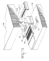
- Figure 1 is an exploded perspective view of the components of a representative PCMCIA card assembly using an input/output electrical connector meeting the requirements of the PCMCIA open systems standard.
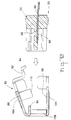
- Figure 3 is an exploded perspective view of the preferred embodiment of this invention showing the main housing subassembly, the shield and the striker plates used in this electrical connector.
- Figure 4 is a top plan view of the housing subassembly of the preferred embodiment of this invention showing the keyed housing spline.
- Figure 5 is a front view of the mating face of the housing subassembly, shown in Figure 4, showing the keyed housing spline and the position of the terminals on the lower surface of the keyed housing spline.
- Figure 6 is a bottom plan view of the housing subassembly shown in Figures 4 and 5 showing the terminals on the bottom surface of the keyed housing spline.
- Figure 7 is a side sectional view taken along the section lines 7-7 in Figure 4 which extends through one of the make first, break last terminals located on the ends of the terminal array..
- Figure 8 is a side sectional view taken along the section lines 8-8 in Figure 4 which extends through one of the signal terminals located between the make first, break last terminals.
- Figure 9 is a perspective view of the housing subassembly showing the terminal mating surface.
- Figure 12 is a side sectional view showing the manner in which the housing subassembly in positioned in the shield during fabrication of the connector.
- FIG. 1 shows the basic elements of a PCMCIA card assembly or frame kit 2 that uses an input/output electrical connector or header 18 complying with the PCMCIA Open System Standard.
- This PCMCIA card assembly 2 comprises an interface between a computer or other processor and a local area network, modem or similar system communicating with the computer or processor.
- the heart of the PCMCIA card assembly 2 is a PCMCIA card or memory card 4.
- This card 4 is a printed circuit board. Circuit elements or components used for storing, receiving, transmitting or other standard data processing or manipulation are mounted on this printed circuit board.
- PCMCIA card 2 can contain all of the circuit elements necessary to implement a modem, or it can comprise a network interface card.
- the PCMCIA card assembly also includes a top cover 6 and a bottom cover 8.
- This PCMCIA card assembly 2 is approximately 85 mm. long and 55 mm. wide.
- PCMCIA card assembly 2 has two electrical connectors located at opposite ends.
- a socket or receptacle connector 10 is located at one end.
- This receptacle connector 10 includes socket terminals of conventional construction which mate with pins protruding into a card slot on a computer when the PCMCIA card assembly 2 is mated with a computer. Insertion of the card into the slot and mating engagement of this connector with the computer is conventional in nature and need not be shown.
- An input/output electrical connector or header or card I/O connector 18 is located at the opposite end of the card assembly 2. This header 18 is mounted in a peripheral frame forming part of the lower cover 8 and is soldered to the card 4 in a cutout or notch on this end of the card.
- Figure 2 shows the mating face of the preferred embodiment of the PCMCIA Card I/O connector 18.
- Figure 3 shows the rear face of the connector 18 and shows three different elements, the housing subassembly including the molded insulative housing 20 and the terminals 60, the clamshell shield 80, and two striker plates 76.
- Figures 4-8 are detailed two dimensional views of the housing subassembly.
- This card I/O connector is relatively small.
- Card I/O connector 18 is approximately 17.40 mm wide, 4.40 mm high and 8.80 mm deep.
- the molded insulative housing 20 is a one piece member comprising a base 22 with two mounting arms 30 and a keyed housing spline 38 extending from the housing base 22 toward the front of the card I/O connector 18.
- the base top surface 24 and base bottom surface 26 are substantially identical and are mutually parallel.
- the base rear surface 28 is substantially flat and the terminals 60 extend through the base mounting surface.
- the keyed housing spline 38 is an integrally molded extension from the front of the housing base 22. This keyed housing spline 38 is substantially parallel to the top and bottom base surfaces 24, 26 and is positioned between these two surfaces.
- the side ends of the keyed housing spline 38 are spaced from the two base mounting arms 30, and gaps are formed between the spline 38 and each mounting arm 30.
- Slots 34 extend through the base 22 in alignment with these gaps between the spline 38 and the mounting arms 30.
- the mounting arms 30 are substantially C-shaped in cross section with the slots 34 being positioned in the center of the C-shaped cross section.
- Crimp grooves 32 extend between the front and rear along the outer surface of each mounting arm 30.
- the base 22 also includes a rib 36 located on the top and bottom surfaces. The crimp grooves 32 and the housing ribs 36 are used to mount the shield 80 on the molded housing 20 in a manner to be subsequently described in more detail.
- the blade-like keyed housing spline 38 extending from the front of the base 22 has a keying face 48 and an oppositely directed contact face 50.
- the entire contour of the keying face 48 comprises keying means matable with a compatible female keying surface (not shown) on the cable connector 16. Both of these keying surfaces are defined by the PCMCIA Open Systems Standard so that noncomplementary connectors cannot be mated. For example, a cable connector having a local area network keying configuration cannot be mated with an card I/O connector having a modem keying configuration.
- the keying means for the card I/O connector 18 comprises a series of key tongues 42 protruding above the centerline of the spline contact surface 50 and key grooves 44 recessed below the contact surface 50. It is the relative position of keys 42 and grooves 44, along with the orientation of the angled or chamfered spline side edges 40 that form the keying configuration or keying means on card I/O connector 18.
- Contact terminals 60 extend along contact surface 50 on the keyed spline 38.
- This contact surface 50 is on the face on the oppcsite side of the keying spline face 48 where the tongues 42 and the grooves 44 are located.
- This contact surface 50 extends from the front of housing base 22 to the forward spline edge 46.
- a spline rib 54 molded as part of the housing spline 38 extends between the forward spline edge and the forward end 72 of each terminal 60. These spline ribs 54 protect the terminals during mating so that the mating cable connector does not bend the terminals.
- the embodiment of the card I/O connector 18 depicted herein also includes a spline ridge 56 which extends from the base 22 to the spline forward edge 46. Inspection of Figure 10 shows that this spline ridge is located between two terminals 60. The spacing between the spline ridge 56 and each adjacent terminal is the same as the spacing between adjacent terminals.
- the spline ridge 56 is a molded replacement for an omitted terminal.
- a spline ridge 56 is molded when a terminal is omitted from the card I/O connector 2. Terminals can be omitted when the terminal in that position is not used by the specific PCMCIA card application with which that connector is to be used.
- a recess 58 is located at the juncture between the base 22 and the spline 38 next to the spline contact surface 50. This recess 58 is also formed during the molding process and will be subsequently discussed in more detail.
- the forward ends 72 of the longer make first, break last terminals are closer to the forward spline edge 46 than the forward ends 72 of the other signal terminals 64, so that this terminals engage mating cable connector terminals first (make first) and disengage after the other terminals during unmating (make last).
- these make first, break last terminals 62 are ground terminals and their make first, break last configuration prevents undesirable signal levels from being transmitted over the other signal terminals.
- Each of the terminals 60, positioned along the contact surface 50 is positioned behind a spline rib 54 as previously described.
- the bottom 68 of each terminal 60 is slightly below the portion of the contact surface 50 immediately adjacent each terminal and the top surface 66 of each terminal protrudes above the aligned spline ridge 56.
- Each terminal has a rear section 74 extending from the rear of the housing base 44. This rear section 74 is configured so that the terminal can be surface mount soldered to a corresponding surface mount pad 12 on the PC card 4.
- Each terminal 60 also extends through the housing base 22 and the housing is insert molded around the terminals 60. This insert molding step will be subsequently discussed in more detail.
- Each terminal 60 extends from the housing base 22 through the recess 58 at the juncture of the base and spline. This relative position between the terminals 60 and the recess 58 is also a function of the insert molding process to be discussed subsequently.
- each slot 34 extends through the housing base 22 and are aligned with the gap between the mounting arms 30 and the housing spline 38.
- Each slot 34 receives a striker plate 76 inserted from the rear of the housing.
- each striker plate 76 includes a rectangular opening 78 adjacent the front edge of the striker plate. This opening 78 is positioned to engage a latch on the cable connector 16 when the cable connector and the card I/O connector are mated. The position of this latch on the cable connector 16 is specified by PCMCIA Card Standard - Release 2.0.
- this central opening 94 is generally rectangular with two chamfered sections located at the top corners where the upper frame section 96 joins the two side frame sections 100.
- the contour formed by this central opening 94 forms the peripheral mating surface for engagement with the cable connector 16.
- This contour is for a Type II configuration defined by PCMCIA Open Systems Standard, Release 2.0. This standard does not, however, require that this peripheral mating contour be formed by the shield or by portions of a shield in a common plane.
- Figures 11 and 12 show two of the steps in the fabrication the I/O card connector 18.
- the insulative housing 20 is insert molded around the terminals 60.
- Figure 12 shows the extraction from the mold of the insert molded subassembly including the terminals embedded in the housing.
- the mold used in this insert molding process includes three pieces.
- the top mold piece includes a cavity, not shown, which molds the top surface of the housing 20.
- This top mold piece engages the mold base 118 which contains a mold cavity the molds the lower housing surface.
- the arrow on the top mold piece 116 shows that the top mold piece has raised after the housing has been molded.
- the lower arrow shows that the housing subassembly has been ejected from the cavity in the mold base 118.
Abstract

Description
- This invention is related to electrical connectors for providing an interface between a printed circuit card and an external device or component. More specifically, this invention is related to an input/output electrical connector which can be used with a PC Card, such as a PCMCIA card assembly. Still more specifically, this invention is related to an input output electrical connector or header that complies with the PCMCIA Open System Standard for I/O Connectors and can be used as a local area network connector, a modem simple implementation connector, or a modem multifunctional connector.
- The Personal Computer Memory Card International Association (PCMCIA) is an organization composed of a number of manufacturers of PC cards and related peripheral equipment. This organization has established standards or specifications for memory cards used with computers and especially for use with laptop, notebook or portable computers. PC cards which meet this PCMCIA standard are credit card-sized wafers. The dimensions of a PCMCIA standard card assembly are 85 mm. in length and 55 mm. wide. These cards employ a high density electrical connector to connect the PC card to the personal computer or other computing equipment with which the PCMCIA card is to be used. This high density electrical connector includes a number of sockets which mate with pins on the computer. This high density connector meets the requirements of PC Card standard, Release 2.0, PCMCIA (September 1991) which defines the PC Card's physical outline and the connector system qualification test parameters, including reliability, durability and environmental test parameters.
- PCMCIA cards can be used with laptop or notebook personal computers to provide an interface to a peripheral device such as an external floppy disk drive. PCMCIA cards can also be used as memory cards, including Flash, EPROM, DRAM or as other memory cards. When used in these applications the PCMCIA cards are inserted into a card slot and into engagement with a standard high density connector mounted on a printed circuit board in the computer.
- PCMCIA cards are not limited to use as memory cards or external floppy disk drives that have no external connection other than their connection to the computer. These cards can also be used as part of an external modem which is connected to an external telephone line or as part of a local area network interface assembly. Modems and local area networks in turn require specific cable interconnections. For example, a modem will typically require an RJ-11 six position connector for an interface to a standard telephone line. Different local area networks typically require different connections. These local area network interconnections include RJ-45 eight position connectors for shielded or unshielded twisted pair, coaxial connections for Ethernet and fiber optic connections for FDDI local area networks. One approach to implementing these various connections is to use a cable assembly with male and female I/O connectors to the PCMCIA card at one cable end and the specific media connector interface on the other cable end. PCMCIA Card Standard Release 2.0 defines an Open System Standard including a common male and female I/O interface. This Open System Standard includes three distinct mating key configurations. One key is for local area network applications including Ethernet, Token Ring, Arcnet, Fast Ethernet and ATM. A second key configuration is for Modem Simple Implementation. A third key configuration is for Modem Multifunctional. These Open System mating interface key configurations are formed on a keyed housing spline which comprises a generally flat protruding blade on the insulative housing of the Card I/O connector mounted on the PCMCIA card assembly. Different tongue and groove configurations are formed on one surface of this keying spline. Prior art Open System compatible connectors use keys selectively insertable in grooves on the keyed spline to define these different key configurations. Individual keys or tongues are 1.60 mm wide and protrude above the spline surface by 0.250 mm. Grooves are similarly 1.60 mm wide and are recessed into the spline surface by 0.250 mm. Adjacent keys and grooves are located on 4.0 mm centerlines. Side edges of the keyed spline are angled to provide additional keying to distinguish between the three standard configurations.
- Pin terminals are located side by side on the opposite surface of the keyed spline. These standard connectors include up to fifteen pins spaced apart on 0.80 mm centerlines.
Pins 1 and 15 are make first, break last contacts having a length of 3.9 mm. Pins 2-14 are signal contacts have a length of 3.0 mm. The front ends of the longer make first, break last contacts on the ends of the terminal array are closer to the forward edge of the keyed connector spline than the signal contacts. Therefore, the make first, break last contacts will engage corresponding contacts of the standard cable connector while the signal contacts are disengaged to prevent extraneous signals or excessive signal levels from being transmitted on pins 2-14. - The Open System Standard defining the I/O configuration is intended to promote availability of multi-sourced I/O connectors satisfying PCMCIA-mandated design criteria by promoting uniform implementation interfaces. However, there is no requirement that all I/O connectors meet this standard. Nonstandard I/O connectors will function properly provided that compatible male and female configurations are used. There are a number of prior configurations which predate the Open System Standards. U.S. Patent 5,330,360 discloses a memory card frame kit which uses an I/O connector that does not employ the keying configuration mandated by the PCMCIA Open System Standard. That connector includes an array of pin terminals located on one side of a housing spline, but does not employ tongue and groove keys on the opposite spline surface. That connector also employs an insulative housing with a D-shaped mating interface. A keying rib extends between the D-shaped peripheral mating interface and the centrally positioned spline on commercially available configurations of this connector. Other commercially available versions of I/O connectors include a mating interface in which the outer periphery is defined by a shield with distinct housing keys located on the sides of the mating interface. Versions of these connectors manufactured by AMP Incorporated employ insert molded housings in which the terminals are held in position in a mold by molding pins and the housing is then injection molded around the terminals and the molding pins. The sections of the mold move towards and away from the housing spline and perpendicular to the orientation of the terminals. The molding pins also move away from the housing and small holes, through which the terminals are exposed are left in the conventionally injected molded housing.
- I/O connectors that meet the PCMCIA Open System Standard for I/O connectors are also commercially available. Honda Connectors markets and sells a Type I Open System shielded I/O connector in which the shield defines the outer mating interface. The shield on that connector is wrapped around an insulative housing, and a keyed spline extends from the front of the main body of the insulative housing. Grooves are molded on the housing spline and discrete tongues or male keys are inserted into these grooves to form the distinct keyed configurations defined by the Open Systems Standard. The insulative housing includes hold down protrusions. Each protrusion contains a rivet to secure the I/O connector to an edge of the PC card. Individual contacts are inserted through the main body of the insulative housing into position on the lower surface of the housing spline. The forward edges of the make first break last contacts are exposed along the front edge of the spline.
- Foxconn Connectors also markets an card I/O connector which meets the PCMCIA Open System Standard. This latter card I/O connector is a thicker Type II connector in which the peripheral mating interface is formed by the insulative housing. A shield is inserted around a portion of the housing. This shield does not extend to the forward edge of the housing, leaving an unshielded gap. This prior art connector also includes contacts that are inserted through holes in the housing base and that are positioned on the lower edge of the housing spline. Individual keys are similarly inserted in molded grooves on the spline lower surface to define different keying configurations. The front ends of the make first, break last contacts are also exposed along the forward edge of the housing spline.
- The input/output electrical connector disclosed and claimed herein is specifically intended for use in a PCMCIA card assembly. Although specifically intended for use in a connector which meets the requirement of a Open System Standard, this connector can also be used with other versions of PCMCIA card assemblies and other high density, small PC card applications. This input/output connector includes an insulative housing which is insert molded around terminals. The terminals are positioned along one surface of a housing spline which is formed by a section of the mold which is shifted parallel to the terminals during extraction of the insert molded housing subassembly from the housing mold. The housing spline includes molded ridges extending between the forward edge of the housing spline and the forward end of each terminal to protect the terminals when a cable connector is connected to the edge mounted card I/O connector containing these terminals.
- More specifically, the card I/O connector includes a molded insulative housing having a base and a keyed spline extending from the front of the base. An array of terminals are positioned along one surface of the keyed spline. The insulative housing is insert molded around the portion of the terminals extending through the base of the housing. The rear portion of the terminals are configured to mate with a PC Card, and in the preferred embodiment, the rear terminal portions comprise surface mount terminal sections. The keyed spline is molded using a mold slide which is shifted parallel to the portion of the terminals positioned along the lower surface of the spline and parallel to the tongue and groove keys which are formed along the top of the spline. The small terminal contacts can then be held in position by the mold. Small positioning pins need not be included in the mold. These small mold pins are relatively fragile parts of a mold and would tend to reduce its life or increase mold maintenance. By providing lead in sections in the mold, the array of closely spaced small pins can be inserted and properly positioned while reducing the possibility of damaging the pins. The use of a mold slide to form this spline also permits different keyed splines to be molded, by simply using the appropriate mold slide. The top and bottom mold cavities need not be changed. Different keying configurations can therefore be efficiently molded without the need for a secondary operation in which keys are inserted in grooves in distinct patterns.
- The keyed spline includes molded ribs in front of each terminal. These ribs protect the terminals during mating so that a mating connector cannot engage the front end of a terminal and bend it back. Since the keyed spline is formed by a mold slide which moves parallel to the terminals, these ribs can be easily molded. These ribs are especially important when used with relatively longer make first, break last pins which are closer to the forward edge of the spline and are therefore otherwise more likely to be damaged.
- Perhaps, most significantly, this small connector typically including fifteen terminals, an insulative housing, two striker plates for mechanically engaging a mating cable connector, and a single piece clamshell shield is also readily adaptable to automation to reduce manufacturing cost.
- Embodiments of the invention will now be described by way of example with reference to the accompanying drawings in which:
- Figure 1 is an exploded perspective view of the components of a representative PCMCIA card assembly using an input/output electrical connector meeting the requirements of the PCMCIA open systems standard.
- Figure 2 is a perspective view of the preferred embodiment of an input/output electrical connector which meets the requirements of the PCMCIA open systems standard.
- Figure 3 is an exploded perspective view of the preferred embodiment of this invention showing the main housing subassembly, the shield and the striker plates used in this electrical connector.
- Figure 4 is a top plan view of the housing subassembly of the preferred embodiment of this invention showing the keyed housing spline.
- Figure 5 is a front view of the mating face of the housing subassembly, shown in Figure 4, showing the keyed housing spline and the position of the terminals on the lower surface of the keyed housing spline.
- Figure 6 is a bottom plan view of the housing subassembly shown in Figures 4 and 5 showing the terminals on the bottom surface of the keyed housing spline.
- Figure 7 is a side sectional view taken along the section lines 7-7 in Figure 4 which extends through one of the make first, break last terminals located on the ends of the terminal array..
- Figure 8 is a side sectional view taken along the section lines 8-8 in Figure 4 which extends through one of the signal terminals located between the make first, break last terminals.
- Figure 9 is a perspective view of the housing subassembly showing the terminal mating surface.
- Figure 10 is an enlarged view of a portion of the contact surface and the terminals on the housing subassembly shown within the circle 10-10 in Figure 9.
- Figure 11 is a perspective view showing the manner in which the housing subassembly is formed by insert molding the terminals in the insulative housing.
- Figure 12 is a side sectional view showing the manner in which the housing subassembly in positioned in the shield during fabrication of the connector.
- Figure 1 shows the basic elements of a PCMCIA card assembly or
frame kit 2 that uses an input/output electrical connector orheader 18 complying with the PCMCIA Open System Standard. ThisPCMCIA card assembly 2 comprises an interface between a computer or other processor and a local area network, modem or similar system communicating with the computer or processor. The heart of thePCMCIA card assembly 2 is a PCMCIA card ormemory card 4. Thiscard 4 is a printed circuit board. Circuit elements or components used for storing, receiving, transmitting or other standard data processing or manipulation are mounted on this printed circuit board. For example,PCMCIA card 2 can contain all of the circuit elements necessary to implement a modem, or it can comprise a network interface card. The specific components to be mounted on this card or printed circuit board are not shown, since the specific circuits are not relevant to the input/output connector that is the subject of the invention disclosed herein. The PCMCIA card assembly also includes atop cover 6 and abottom cover 8. ThisPCMCIA card assembly 2 is approximately 85 mm. long and 55 mm. wide. -
PCMCIA card assembly 2 has two electrical connectors located at opposite ends. A socket orreceptacle connector 10 is located at one end. Thisreceptacle connector 10 includes socket terminals of conventional construction which mate with pins protruding into a card slot on a computer when thePCMCIA card assembly 2 is mated with a computer. Insertion of the card into the slot and mating engagement of this connector with the computer is conventional in nature and need not be shown. An input/output electrical connector or header or card I/O connector 18 is located at the opposite end of thecard assembly 2. Thisheader 18 is mounted in a peripheral frame forming part of thelower cover 8 and is soldered to thecard 4 in a cutout or notch on this end of the card.Surface mount pads 12 are located in this notched region adjacent to the edge of thecard 4. Two mountingholes 14 are located on opposite sides of the array ofpads 12. This input/output connector orheader 18 mates with acable connector 16. Both thecable connector 16 and the card I/O connector 18 comply with the PCMCIA Open System Standard as more specifically described in Release 2.0, Section 3, I/O Connector Specification. - Figure 2 shows the mating face of the preferred embodiment of the PCMCIA Card I/
O connector 18. Figure 3 shows the rear face of theconnector 18 and shows three different elements, the housing subassembly including the moldedinsulative housing 20 and theterminals 60, theclamshell shield 80, and twostriker plates 76. Figures 4-8 are detailed two dimensional views of the housing subassembly. This card I/O connector is relatively small. Card I/O connector 18 is approximately 17.40 mm wide, 4.40 mm high and 8.80 mm deep. - The molded
insulative housing 20 is a one piece member comprising a base 22 with two mountingarms 30 and akeyed housing spline 38 extending from thehousing base 22 toward the front of the card I/O connector 18. The basetop surface 24 andbase bottom surface 26 are substantially identical and are mutually parallel. The baserear surface 28 is substantially flat and theterminals 60 extend through the base mounting surface. Thekeyed housing spline 38 is an integrally molded extension from the front of thehousing base 22. This keyedhousing spline 38 is substantially parallel to the top and bottom base surfaces 24, 26 and is positioned between these two surfaces. The side ends of thekeyed housing spline 38 are spaced from the twobase mounting arms 30, and gaps are formed between thespline 38 and each mountingarm 30. -
Slots 34 extend through the base 22 in alignment with these gaps between thespline 38 and the mountingarms 30. As seen in Figure 5, the mountingarms 30 are substantially C-shaped in cross section with theslots 34 being positioned in the center of the C-shaped cross section. Crimpgrooves 32 extend between the front and rear along the outer surface of each mountingarm 30. The base 22 also includes arib 36 located on the top and bottom surfaces. Thecrimp grooves 32 and thehousing ribs 36 are used to mount theshield 80 on the moldedhousing 20 in a manner to be subsequently described in more detail. - The blade-like keyed
housing spline 38 extending from the front of thebase 22 has a keyingface 48 and an oppositely directedcontact face 50. The entire contour of the keyingface 48 comprises keying means matable with a compatible female keying surface (not shown) on thecable connector 16. Both of these keying surfaces are defined by the PCMCIA Open Systems Standard so that noncomplementary connectors cannot be mated. For example, a cable connector having a local area network keying configuration cannot be mated with an card I/O connector having a modem keying configuration. The keying means for the card I/O connector 18 comprises a series ofkey tongues 42 protruding above the centerline of thespline contact surface 50 andkey grooves 44 recessed below thecontact surface 50. It is the relative position ofkeys 42 andgrooves 44, along with the orientation of the angled or chamfered spline side edges 40 that form the keying configuration or keying means on card I/O connector 18. -
Contact terminals 60 extend alongcontact surface 50 on the keyedspline 38. Thiscontact surface 50 is on the face on the oppcsite side of thekeying spline face 48 where thetongues 42 and thegrooves 44 are located. Thiscontact surface 50 extends from the front ofhousing base 22 to theforward spline edge 46. Aspline rib 54, molded as part of thehousing spline 38 extends between the forward spline edge and theforward end 72 of each terminal 60. Thesespline ribs 54 protect the terminals during mating so that the mating cable connector does not bend the terminals. The embodiment of the card I/O connector 18 depicted herein also includes aspline ridge 56 which extends from the base 22 to the splineforward edge 46. Inspection of Figure 10 shows that this spline ridge is located between twoterminals 60. The spacing between thespline ridge 56 and each adjacent terminal is the same as the spacing between adjacent terminals. Thespline ridge 56 is a molded replacement for an omitted terminal. As will be subsequently described, aspline ridge 56 is molded when a terminal is omitted from the card I/O connector 2. Terminals can be omitted when the terminal in that position is not used by the specific PCMCIA card application with which that connector is to be used. Arecess 58 is located at the juncture between the base 22 and thespline 38 next to thespline contact surface 50. Thisrecess 58 is also formed during the molding process and will be subsequently discussed in more detail. - The
terminals 60 are stamped and formed, and in the preferred embodiment, these terminals are formed from a material such as brass. These terminals are substantially square in cross section and are approximately .25 mm on each side. The card I/O connector 18 conforming to the PCMCIA Open Systems Standard employs up to fifteenterminals 60. The centerline spacing betweenadjacent terminals 60 is 0.8 mm. A row ofterminals 60 includes two types ofterminals terminals 62 in positions one and fifteen on the ends of the array of terminals function as make first, break last terminals and are longer than theother signal terminals 64. The length of the make first, break last terminals is 3.9 mm., and the length of the other signal terminals is 3.0 mm. The forward ends 72 of the longer make first, break last terminals are closer to theforward spline edge 46 than the forward ends 72 of theother signal terminals 64, so that this terminals engage mating cable connector terminals first (make first) and disengage after the other terminals during unmating (make last). Generally these make first, breaklast terminals 62 are ground terminals and their make first, break last configuration prevents undesirable signal levels from being transmitted over the other signal terminals. - Each of the
terminals 60, positioned along thecontact surface 50 is positioned behind aspline rib 54 as previously described. The bottom 68 of each terminal 60 is slightly below the portion of thecontact surface 50 immediately adjacent each terminal and thetop surface 66 of each terminal protrudes above the alignedspline ridge 56. Each terminal has arear section 74 extending from the rear of thehousing base 44. Thisrear section 74 is configured so that the terminal can be surface mount soldered to a correspondingsurface mount pad 12 on thePC card 4. Each terminal 60 also extends through thehousing base 22 and the housing is insert molded around theterminals 60. This insert molding step will be subsequently discussed in more detail. Each terminal 60 extends from thehousing base 22 through therecess 58 at the juncture of the base and spline. This relative position between theterminals 60 and therecess 58 is also a function of the insert molding process to be discussed subsequently. - The two
slots 34 extend through thehousing base 22 and are aligned with the gap between the mountingarms 30 and thehousing spline 38. Eachslot 34 receives astriker plate 76 inserted from the rear of the housing. As shown in Figure 3, eachstriker plate 76 includes arectangular opening 78 adjacent the front edge of the striker plate. Thisopening 78 is positioned to engage a latch on thecable connector 16 when the cable connector and the card I/O connector are mated. The position of this latch on thecable connector 16 is specified by PCMCIA Card Standard - Release 2.0. - The
striker plates 76 are inserted intoslots 34 prior to assembly of theshield 80 on thehousing 20. Theshield 80 is a clamshell stamped and formed member. The preferred embodiment of the shield is formed from stainless steel.Shield 80 has atop section 86 and abottom section 88. Twoshield tabs 82 are bent down from thetop shield section 86, as best seen in Figure 3. Theseshield tabs 82 also includedistal tab sections 84 that are in turn bent down from theshield tab 82. These distal tab sections are dimensioned to fit in the twoholes 14 on thePC Card 4 that are shown in Figure 1. These shield tabs can be soldered to thePC Card 4 and serve to mechanically secure the card I/O connector 18 to thePC Card 4. - The
shield 80 also includes aframe section 92 located between thetop shield section 86 and thebottom shield section 88. Thetop shield section 86 is joined to theupper frame section 96 and thebottom shield section 88 is joined to thelower frame section 98. This frame section is best shown in Figure 2. Theframe section 92 also includesside frame sections 100 which join theupper frame section 96 to thelower frame section 98 at both ends. Acentral opening 94 is formed by the upper, lower and side frame sections, all of which are in a common vertical plane perpendicular to thehousing spline 38, to theterminals 60 and to the direction in which thecable connector 16 is inserted into mating engagement with the card I/O connector 18. As shown in Figure 2, thiscentral opening 94 is generally rectangular with two chamfered sections located at the top corners where theupper frame section 96 joins the twoside frame sections 100. The contour formed by thiscentral opening 94 forms the peripheral mating surface for engagement with thecable connector 16. This contour is for a Type II configuration defined by PCMCIA Open Systems Standard, Release 2.0. This standard does not, however, require that this peripheral mating contour be formed by the shield or by portions of a shield in a common plane. -
Shield 80 also includes contact tabs for establishing ground contacts with both the card assembly and with thecable connector 18.Spring tabs 104 are struck from the top and bottom shield sections. Thesetabs 104 engage thetop cover 6 and thebottom cover 8 when the card I/O connector 18 is attached as part of thecard assembly 2. Acantilever spring section 90 extends from the inner edge of theupper frame section 96 toward the rear of the connector. Thiscantilever spring section 90 is shown in Figure 12 where theshield 80 is shown in its partially open position prior to assembly to thehousing 20. Thiscantilever spring section 90 is positioned to engage a shield on thecable connector 18 when mated with the card I/O connector 18. Thecantilever spring section 90 extends between thetop shield section 86 and thebottom shield section 88.Cantilever spring section 90 also extends between thetop shield section 86 and the keying surface on thehousing spline 38 when the shield is mounted on the moldedhousing 20. - The
shield 80 surrounds the moldedhousing 20 and the mountingarms 30 support theshield 80.Side sections 102 extend inwardly from thetop shield section 86 and thebottom shield section 88 and secure theshield 80 to the mounting arms. The ends of theside shield sections 102 are crimped inwardly into thecrimp grooves 32 on the outside of the mountingarms 30 to secure theshield 80 to thehousing 20.Slots 106 located on the top and bottom sections of theshield 80 are dimensioned to receiveribs 36 molded on the top and bottom faces of thehousing base 22 to provide additional retention of theshield 80 on thehousing 20.Side shield tabs 108 extend downwardly from both sides thetop shield section 86. Theseside shield tabs 108 are dimensioned so that they engage the PC card to support the card I/O connector 18. Theseside shield tabs 108 can be soldered to pads on the printed circuit board to provide additional mechanical security.Lateral shield tabs 110 also extend from the sides of theshield 80. Theselateral shield tabs 110 are located adjacent to the front of theshield 80 and extend from theside frame sections 100. Thelateral shield tabs 110 initially are bent rearward relative to theframe section 92 and then extend laterally out from each side of theshield 80. These laterally extendingtabs 110 are inserted in slots on the PC card assembly frame on each side of the cutout section in which the card I/O connector 18 is mounted so that theconnector 18 and the PC card to which it is attached are properly positioned relative to the card frame and to thebottom cover 8. - As best shown in Figure 2, each part of the
shield frame section 92 is joined to a portion of the shield extending rearward and perpendicular to the plane of the shield section. Thisframe section 92, which forms the peripheral mating surface of theopening 94 through whichcable connector 16 is inserted during mating, is therefore relatively robust and rigid and will not significantly deform during connector mating. In particular, thetop shield section 86 will not tend to bow outward during insertion of acable connector 16 throughopening 94. Since the keying surface onspline 38 faces thistop section 86, any tendency of the top section to bow outwardly during mating could permit insertion of a cable connector with the wrong keying configuration. - Figures 11 and 12 show two of the steps in the fabrication the I/
O card connector 18. Theinsulative housing 20 is insert molded around theterminals 60. Figure 12 shows the extraction from the mold of the insert molded subassembly including the terminals embedded in the housing. The mold used in this insert molding process includes three pieces. The top mold piece includes a cavity, not shown, which molds the top surface of thehousing 20. This top mold piece engages themold base 118 which contains a mold cavity the molds the lower housing surface. The arrow on thetop mold piece 116 shows that the top mold piece has raised after the housing has been molded. The lower arrow shows that the housing subassembly has been ejected from the cavity in themold base 118. The mold used to insert mold the housing around theterminals 60 also includes a third section in form of amold slide 114. The arrow in Figure 11 shows that thismold slide 114 moves in a direction parallel to the interface between thetop mold piece 116 and themold base 118. The first step in fabricating the housing subassembly is to positionterminals 60 on a carrier strip as shown in Figure 11 in the mold cavity between thetop mold piece 116 and themold base 118. Theterminals 60 are joined to the carrier strip at the rear, and the forward ends of theterminals 60 are separate. The terminals extend into the mold cavity toward themold slide 114. After the terminals are positioned in the cavity in thebottom mold base 118, themold slide 114 moves into position. Then thetop mold piece 116 is moved into the closed position. Themold slide 114 has an internal cavity which includes amold surface 112 which forms the contact surface of thehousing spline 38. Themold surface 112 also include a series of grooves in which the individual terminals are positioned during the insert molding process. The front portion of themold surface 112 extends slightly forward of the remainder of the mold front face and each groove in this mold surface includes a lead-in that aligns the individual terminals and insures that the terminals are properly positioned in the grooves. This portion of the mold is too small to be seen in Figure 11. Since this portion of themold surface 112 extends beyond the surrounding area on the front of the mold slide, therecess 58 at the juncture of the housing base and thespline 38 is formed. The opposite side of themold surface 112 forms the tongue and groove configuration of the keying surface onspline 38. Since thetongues 42 andgrooves 44 are parallel to theterminals 60, themold slide 114 can be withdrawn parallel to thetongues 42 andgrooves 44 and to theterminals 60 after plastic has been injected around the terminals. - Molding the
housing spline 38 in this manner has several advantages. Since a number of keying configurations may be required on the spline, only the mold slide needs to be changed to mold a different connector housing. Since each configuration of the molded spline is molded with only this simple mold change, there is no need to use the prior art expedient of inserting additional keys in a common spline configuration to form different keying configurations. These additional keys can fall out during use and require an additional assembly operation that adds to the manufacturing cost. The grooves on themold surface 112 of the mold slide also position the terminals in the mold without the need for additional pins to hold the terminals in position. Thespline ribs 54 protecting the front of theterminals 60 are also easily molded using this approach because they are aligned with the terminals. Insert molding also provides a tight fitting interface between theterminals 60 and thehousing base 22. Insert molding also facilitates the fabrication of connectors including only a portion of the terminals. If one or more terminals is unnecessary for a given application, it can be omitted. The omitted terminals are simply punched out of the terminal lead frame before positioning the lead frame in the mold. Plastic injected into the mold will then fill up that portion of the mold cavity otherwise occupied by the omitted terminal. There will be no opening in the base 22 caused by the omission of one or more terminals. The groove on themold surface 112 will also be filled by the injected plastic resulting in the formation of thespline ridges 56 shown in Figures 9 and 10. - After the housing assembly has been molded by this insert molding step, the
stiker plates 76 are first inserted in the housing and then theshield 80 is positioned around the housing. Figures 2, 3 and 12 show the simple attachment of theclam shell shield 80 to thehousing 20. - These assembly and fabrication steps are especially adapted to the automated assembly of card I/
O connector 18. There is no need to individually insert or otherwise handle the terminals and the terminal insertion step required by other assembly operations is eliminated. Small core pins which can be damaged and not needed to mold cavities in the housing or to position the terminals for insert molding. The shield is used to secure the entire connector to the PC card eliminating the expensive step of assembling rivets to the connector. The shield is also formed in a relatively rigid configuration for more reliable keyed connector mating. Although the preferred embodiment of this connector disclosed herein is compatible with the PCMCIA Open System standard it should be understood that the advantages of this insert molded product and this shield configurations are also applicable to Closed System or proprietary PCMICA connector configuration and to other small high density electrical connectors. Therefore the embodiment depicted herein is representative and is not the sole example of an electrical connector in accordance with the invention as disclosed and claimed herein.
Claims (10)
- An input output electrical connector for use in a PCMCIA card assembly, the connector comprising:a molded insulative housing (20) including a base (22) with a keyed housing spline (38) extending forward from the base, the spline having keying means (42, 44) on one face and a contact surface (50) on the opposite face;a plurality of terminals (60) extending side by side through the base and along the housing contact surface with the top of each terminal being exposed along the contact surface, each terminal also extending from the rear (28) of the base for attachment to a card in the PCMCIA card assembly;the connector being characterized in that the terminals (60) are insert molded in the insulative housing (20) with the base (22) being molded around a portion of the terminals extending therethrough and with the contact surface (50) on the housing spline (38) being formed by a mold surface (112) initially positioning the terminals and withdrawn parallel to the terminals.
- The electrical connector of claim 1 wherein at least a portion of the terminals (60) have a forward end (72) inwardly spaced from a forward edge (46) of the housing spline, and the contact surface (50) includes housing spline ribs (54) molded between the forward ends (72) of the terminals and the forward edge (46) of the housing spline.
- The electrical connector of claim 2 wherein each spline rib (54) is formed by the mold surface (112) positioning the terminals along the housing spline.
- The electrical connector of claim 1 wherein at least one of the terminals (60) is a make first, break last terminal (62) with a forward end (72) extending beyond the forward end of the other terminals (64).
- The electrical connector of claim 1 wherein a recess (58) is located at the juncture of the base (22) and the contact surface (50), the recess being formed by withdrawal of the molding surface parallel to the terminals.
- The electrical connector of claim 5 wherein the recess (58) extends into the housing base (22) parallel to the contact surface (50), the housing base extending over the top of the recess.
- The electrical connector of claim 1 wherein at least one molded ridge (56) extends between two terminals (60) on the contact surface, the molded ridge extending from the base (22) to a molded rib (54) located on the forward edge of the housing spline.
- The electrical connector of claim 1 wherein a shield (80) is wrapped around at least a portion of the housing and the terminals, the shield having at least one tab means (82) for securing the shield to the card and for securing the electrical connector to the card.
- The electrical connector of claim 8 wherein the insulative housing includes mounting arms (30) extending from two ends of the base (22), the shield being supported by the base and the two mounting arms.
- The electrical connector of claim 9 wherein the housing base (22) includes protruding ribs (36) on opposite sides of the base, the shield including slots (106), the ribs extending into the slots when the shield is mounted on the housing.
Applications Claiming Priority (4)
| Application Number | Priority Date | Filing Date | Title |
|---|---|---|---|
| US39243595A | 1995-02-22 | 1995-02-22 | |
| US39243095A | 1995-02-22 | 1995-02-22 | |
| US392435 | 1995-02-22 | ||
| US392430 | 1995-02-22 |
Publications (3)
| Publication Number | Publication Date |
|---|---|
| EP0729206A2 true EP0729206A2 (en) | 1996-08-28 |
| EP0729206A3 EP0729206A3 (en) | 1997-10-08 |
| EP0729206B1 EP0729206B1 (en) | 2000-08-09 |
Family
ID=27013877
Family Applications (1)
| Application Number | Title | Priority Date | Filing Date |
|---|---|---|---|
| EP96300459A Expired - Lifetime EP0729206B1 (en) | 1995-02-22 | 1996-01-24 | PCMCIA input/output card connector |
Country Status (4)
| Country | Link |
|---|---|
| EP (1) | EP0729206B1 (en) |
| JP (1) | JPH08250217A (en) |
| BR (1) | BR9600710A (en) |
| DE (1) | DE69609644T2 (en) |
Cited By (12)
| Publication number | Priority date | Publication date | Assignee | Title |
|---|---|---|---|---|
| EP0908979A2 (en) * | 1997-10-09 | 1999-04-14 | Molex Incorporated | Card connector assembly |
| EP0908980A2 (en) * | 1997-10-09 | 1999-04-14 | Molex Incorporated | Card connector with improved grounding terminal |
| EP0908978A2 (en) * | 1997-10-09 | 1999-04-14 | Molex Incorporated | Card connector assembly |
| EP0908977A2 (en) * | 1997-10-09 | 1999-04-14 | Molex Incorporated | Card connector with improved grounding terminal |
| EP0784291A3 (en) * | 1996-01-11 | 1999-05-19 | Molex Incorporated | Shielding system for PC cards |
| EP0917254A2 (en) * | 1997-11-17 | 1999-05-19 | Xircom, Inc. | Removable i/o device with integrated receptacles for receiving standard plugs |
| WO1999049540A1 (en) * | 1998-03-25 | 1999-09-30 | Xircom, Inc. | Type iii pcmcia card with integrated receptacles for receiving standard communications plugs |
| KR100327718B1 (en) * | 1997-10-03 | 2002-05-09 | 나가토시 다쯔미 | Electrical connector with a mating portion defined by a metallic shell |
| EP1420478A1 (en) * | 2002-11-14 | 2004-05-19 | Japan Aviation Electronics Industry, Limited | Electrical connector |
| WO2006014541A1 (en) * | 2004-07-07 | 2006-02-09 | Molex Incorporated | Keyed housing for use with small size plug connectors |
| EP2182586A1 (en) * | 2008-10-30 | 2010-05-05 | Samsung Electronics Co., Ltd. | Connector, connector assembly, and display apparatus having the same |
| EP2200126A2 (en) * | 2008-12-16 | 2010-06-23 | Robert Bosch GmbH | Electric plug connector |
Families Citing this family (4)
| Publication number | Priority date | Publication date | Assignee | Title |
|---|---|---|---|---|
| US6773291B1 (en) | 1993-11-12 | 2004-08-10 | Intel Corporation | Compliant communications connectors |
| JP4615646B2 (en) * | 1999-07-21 | 2011-01-19 | オリンパス株式会社 | Printer |
| DE10227602B4 (en) * | 2002-06-20 | 2017-06-22 | Lisa Dräxlmaier GmbH | Method for producing a connector for flat conductors |
| JP5827574B2 (en) * | 2012-01-23 | 2015-12-02 | ヒロセ電機株式会社 | Electrical connector with shield plate |
Citations (3)
| Publication number | Priority date | Publication date | Assignee | Title |
|---|---|---|---|---|
| GB2233596A (en) * | 1989-07-06 | 1991-01-16 | Desbury Ltd | An injection mould for moulding a cable connector housing, having replaceable shape defining mould parts |
| US5201883A (en) * | 1991-08-30 | 1993-04-13 | Kel Corporation | Method of making in-molded plug connector |
| US5330360A (en) * | 1992-08-21 | 1994-07-19 | The Whitaker Corporation | Memory card and connector therefor |
-
1996
- 1996-01-24 DE DE69609644T patent/DE69609644T2/en not_active Expired - Lifetime
- 1996-01-24 EP EP96300459A patent/EP0729206B1/en not_active Expired - Lifetime
- 1996-02-13 BR BR9600710A patent/BR9600710A/en not_active Application Discontinuation
- 1996-02-22 JP JP8060207A patent/JPH08250217A/en active Pending
Patent Citations (3)
| Publication number | Priority date | Publication date | Assignee | Title |
|---|---|---|---|---|
| GB2233596A (en) * | 1989-07-06 | 1991-01-16 | Desbury Ltd | An injection mould for moulding a cable connector housing, having replaceable shape defining mould parts |
| US5201883A (en) * | 1991-08-30 | 1993-04-13 | Kel Corporation | Method of making in-molded plug connector |
| US5330360A (en) * | 1992-08-21 | 1994-07-19 | The Whitaker Corporation | Memory card and connector therefor |
Cited By (21)
| Publication number | Priority date | Publication date | Assignee | Title |
|---|---|---|---|---|
| EP0784291A3 (en) * | 1996-01-11 | 1999-05-19 | Molex Incorporated | Shielding system for PC cards |
| KR100327718B1 (en) * | 1997-10-03 | 2002-05-09 | 나가토시 다쯔미 | Electrical connector with a mating portion defined by a metallic shell |
| EP0908979A3 (en) * | 1997-10-09 | 2000-06-21 | Molex Incorporated | Card connector assembly |
| EP0908980A2 (en) * | 1997-10-09 | 1999-04-14 | Molex Incorporated | Card connector with improved grounding terminal |
| EP0908978A2 (en) * | 1997-10-09 | 1999-04-14 | Molex Incorporated | Card connector assembly |
| EP0908977A2 (en) * | 1997-10-09 | 1999-04-14 | Molex Incorporated | Card connector with improved grounding terminal |
| EP0908979A2 (en) * | 1997-10-09 | 1999-04-14 | Molex Incorporated | Card connector assembly |
| SG79996A1 (en) * | 1997-10-09 | 2001-04-17 | Molex Inc | Card connector with improved grounding terminal |
| EP0908980A3 (en) * | 1997-10-09 | 2000-06-21 | Molex Incorporated | Card connector with improved grounding terminal |
| EP0908978A3 (en) * | 1997-10-09 | 2000-06-21 | Molex Incorporated | Card connector assembly |
| EP0908977A3 (en) * | 1997-10-09 | 2000-06-21 | Molex Incorporated | Card connector with improved grounding terminal |
| EP0917254A2 (en) * | 1997-11-17 | 1999-05-19 | Xircom, Inc. | Removable i/o device with integrated receptacles for receiving standard plugs |
| EP0917254A3 (en) * | 1997-11-17 | 1999-08-04 | Xircom, Inc. | Removable i/o device with integrated receptacles for receiving standard plugs |
| WO1999049540A1 (en) * | 1998-03-25 | 1999-09-30 | Xircom, Inc. | Type iii pcmcia card with integrated receptacles for receiving standard communications plugs |
| EP1420478A1 (en) * | 2002-11-14 | 2004-05-19 | Japan Aviation Electronics Industry, Limited | Electrical connector |
| US6913488B2 (en) | 2002-11-14 | 2005-07-05 | Japan Aviation Electronics Industry, Limited | Electrical connector |
| WO2006014541A1 (en) * | 2004-07-07 | 2006-02-09 | Molex Incorporated | Keyed housing for use with small size plug connectors |
| CN101015095B (en) * | 2004-07-07 | 2012-05-09 | 莫莱克斯公司 | Keyed housing for use with small size plug connectors |
| EP2182586A1 (en) * | 2008-10-30 | 2010-05-05 | Samsung Electronics Co., Ltd. | Connector, connector assembly, and display apparatus having the same |
| EP2200126A2 (en) * | 2008-12-16 | 2010-06-23 | Robert Bosch GmbH | Electric plug connector |
| EP2200126A3 (en) * | 2008-12-16 | 2011-09-07 | Robert Bosch GmbH | Electric plug connector |
Also Published As
| Publication number | Publication date |
|---|---|
| EP0729206A3 (en) | 1997-10-08 |
| EP0729206B1 (en) | 2000-08-09 |
| JPH08250217A (en) | 1996-09-27 |
| BR9600710A (en) | 1997-12-30 |
| DE69609644D1 (en) | 2000-09-14 |
| DE69609644T2 (en) | 2000-12-28 |
Similar Documents
| Publication | Publication Date | Title |
|---|---|---|
| EP0795929B1 (en) | Electric connector assembly with improved retention characteristics | |
| EP0729206B1 (en) | PCMCIA input/output card connector | |
| US9912111B2 (en) | Flippable electrical connector | |
| US5586893A (en) | IC card connector shield grounding | |
| US6447311B1 (en) | Electrical connector with grounding means | |
| US20200203867A1 (en) | Robust, miniaturized card edge connector | |
| US7351106B2 (en) | Electrical connector having an inner printed circuit board | |
| US6347948B1 (en) | Cable connector assembly with improved grounding means | |
| US6585537B1 (en) | Cable end connector with locking member | |
| US5549480A (en) | Unitary connector allowing laterally variant positions of mating contacts of complementary connector | |
| EP2169774B1 (en) | Reduced Size Multi-Pin Male Plug Connector | |
| US6655979B1 (en) | Cable end connector with locking member | |
| US6290530B1 (en) | Electrical connector with improved guiding means | |
| US6645005B2 (en) | Electrical connector assembly with latching metal ears | |
| US7179126B2 (en) | Electrical connector with improved terminals | |
| US6540563B1 (en) | Stacked connector assembly | |
| EP0630080B1 (en) | Circuit board mountable modular phone jack | |
| US7744418B2 (en) | Upright electrical connector | |
| WO1999049540A1 (en) | Type iii pcmcia card with integrated receptacles for receiving standard communications plugs | |
| US5281165A (en) | Electrical connector shroud adapted for shorting bar removal | |
| US6685508B2 (en) | USB connector assembly having reduced mating height | |
| US6371790B1 (en) | Electrical assembly having anti-mismating device | |
| US20200067243A1 (en) | Universal serial bus type-c electrical connector having a reduced length | |
| US6358067B1 (en) | Docking-style intermediate connector | |
| US6409549B1 (en) | Electrical connector |
Legal Events
| Date | Code | Title | Description |
|---|---|---|---|
| PUAI | Public reference made under article 153(3) epc to a published international application that has entered the european phase |
Free format text: ORIGINAL CODE: 0009012 |
|
| AK | Designated contracting states |
Kind code of ref document: A2 Designated state(s): DE FR GB |
|
| PUAL | Search report despatched |
Free format text: ORIGINAL CODE: 0009013 |
|
| AK | Designated contracting states |
Kind code of ref document: A3 Designated state(s): DE FR GB IE IT NL SE |
|
| 17P | Request for examination filed |
Effective date: 19971027 |
|
| GRAG | Despatch of communication of intention to grant |
Free format text: ORIGINAL CODE: EPIDOS AGRA |
|
| 17Q | First examination report despatched |
Effective date: 19990716 |
|
| GRAG | Despatch of communication of intention to grant |
Free format text: ORIGINAL CODE: EPIDOS AGRA |
|
| GRAG | Despatch of communication of intention to grant |
Free format text: ORIGINAL CODE: EPIDOS AGRA |
|
| GRAH | Despatch of communication of intention to grant a patent |
Free format text: ORIGINAL CODE: EPIDOS IGRA |
|
| RIC1 | Information provided on ipc code assigned before grant |
Free format text: 7H 01R 43/24 A, 7H 01R 13/64 B, 7H 01R 12/18 B, 7H 01R 13/405 B, 7H 01R 13/658 B |
|
| GRAH | Despatch of communication of intention to grant a patent |
Free format text: ORIGINAL CODE: EPIDOS IGRA |
|
| GRAA | (expected) grant |
Free format text: ORIGINAL CODE: 0009210 |
|
| RBV | Designated contracting states (corrected) |
Designated state(s): DE FR GB |
|
| AK | Designated contracting states |
Kind code of ref document: B1 Designated state(s): DE FR GB |
|
| ET | Fr: translation filed | ||
| REF | Corresponds to: |
Ref document number: 69609644 Country of ref document: DE Date of ref document: 20000914 |
|
| PLBE | No opposition filed within time limit |
Free format text: ORIGINAL CODE: 0009261 |
|
| STAA | Information on the status of an ep patent application or granted ep patent |
Free format text: STATUS: NO OPPOSITION FILED WITHIN TIME LIMIT |
|
| 26N | No opposition filed | ||
| REG | Reference to a national code |
Ref country code: GB Ref legal event code: IF02 |
|
| PGFP | Annual fee paid to national office [announced via postgrant information from national office to epo] |
Ref country code: FR Payment date: 20100205 Year of fee payment: 15 |
|
| PGFP | Annual fee paid to national office [announced via postgrant information from national office to epo] |
Ref country code: GB Payment date: 20100125 Year of fee payment: 15 Ref country code: DE Payment date: 20100127 Year of fee payment: 15 |
|
| GBPC | Gb: european patent ceased through non-payment of renewal fee |
Effective date: 20110124 |
|
| REG | Reference to a national code |
Ref country code: FR Ref legal event code: ST Effective date: 20110930 |
|
| PG25 | Lapsed in a contracting state [announced via postgrant information from national office to epo] |
Ref country code: FR Free format text: LAPSE BECAUSE OF NON-PAYMENT OF DUE FEES Effective date: 20110131 |
|
| PG25 | Lapsed in a contracting state [announced via postgrant information from national office to epo] |
Ref country code: GB Free format text: LAPSE BECAUSE OF NON-PAYMENT OF DUE FEES Effective date: 20110124 |
|
| REG | Reference to a national code |
Ref country code: DE Ref legal event code: R119 Ref document number: 69609644 Country of ref document: DE Effective date: 20110802 |
|
| PG25 | Lapsed in a contracting state [announced via postgrant information from national office to epo] |
Ref country code: DE Free format text: LAPSE BECAUSE OF NON-PAYMENT OF DUE FEES Effective date: 20110802 |