EP0731373A1 - Liquid crystal display - Google Patents
Liquid crystal display Download PDFInfo
- Publication number
- EP0731373A1 EP0731373A1 EP96301290A EP96301290A EP0731373A1 EP 0731373 A1 EP0731373 A1 EP 0731373A1 EP 96301290 A EP96301290 A EP 96301290A EP 96301290 A EP96301290 A EP 96301290A EP 0731373 A1 EP0731373 A1 EP 0731373A1
- Authority
- EP
- European Patent Office
- Prior art keywords
- liquid crystal
- substrate
- storage capacitance
- array substrate
- colour
- Prior art date
- Legal status (The legal status is an assumption and is not a legal conclusion. Google has not performed a legal analysis and makes no representation as to the accuracy of the status listed.)
- Withdrawn
Links
Images


Classifications
-
- G—PHYSICS
- G02—OPTICS
- G02F—OPTICAL DEVICES OR ARRANGEMENTS FOR THE CONTROL OF LIGHT BY MODIFICATION OF THE OPTICAL PROPERTIES OF THE MEDIA OF THE ELEMENTS INVOLVED THEREIN; NON-LINEAR OPTICS; FREQUENCY-CHANGING OF LIGHT; OPTICAL LOGIC ELEMENTS; OPTICAL ANALOGUE/DIGITAL CONVERTERS
- G02F1/00—Devices or arrangements for the control of the intensity, colour, phase, polarisation or direction of light arriving from an independent light source, e.g. switching, gating or modulating; Non-linear optics
- G02F1/01—Devices or arrangements for the control of the intensity, colour, phase, polarisation or direction of light arriving from an independent light source, e.g. switching, gating or modulating; Non-linear optics for the control of the intensity, phase, polarisation or colour
- G02F1/13—Devices or arrangements for the control of the intensity, colour, phase, polarisation or direction of light arriving from an independent light source, e.g. switching, gating or modulating; Non-linear optics for the control of the intensity, phase, polarisation or colour based on liquid crystals, e.g. single liquid crystal display cells
- G02F1/133—Constructional arrangements; Operation of liquid crystal cells; Circuit arrangements
- G02F1/1333—Constructional arrangements; Manufacturing methods
- G02F1/1335—Structural association of cells with optical devices, e.g. polarisers or reflectors
- G02F1/133509—Filters, e.g. light shielding masks
- G02F1/133514—Colour filters
- G02F1/133516—Methods for their manufacture, e.g. printing, electro-deposition or photolithography
-
- G—PHYSICS
- G02—OPTICS
- G02F—OPTICAL DEVICES OR ARRANGEMENTS FOR THE CONTROL OF LIGHT BY MODIFICATION OF THE OPTICAL PROPERTIES OF THE MEDIA OF THE ELEMENTS INVOLVED THEREIN; NON-LINEAR OPTICS; FREQUENCY-CHANGING OF LIGHT; OPTICAL LOGIC ELEMENTS; OPTICAL ANALOGUE/DIGITAL CONVERTERS
- G02F1/00—Devices or arrangements for the control of the intensity, colour, phase, polarisation or direction of light arriving from an independent light source, e.g. switching, gating or modulating; Non-linear optics
- G02F1/01—Devices or arrangements for the control of the intensity, colour, phase, polarisation or direction of light arriving from an independent light source, e.g. switching, gating or modulating; Non-linear optics for the control of the intensity, phase, polarisation or colour
- G02F1/13—Devices or arrangements for the control of the intensity, colour, phase, polarisation or direction of light arriving from an independent light source, e.g. switching, gating or modulating; Non-linear optics for the control of the intensity, phase, polarisation or colour based on liquid crystals, e.g. single liquid crystal display cells
- G02F1/133—Constructional arrangements; Operation of liquid crystal cells; Circuit arrangements
- G02F1/136—Liquid crystal cells structurally associated with a semi-conducting layer or substrate, e.g. cells forming part of an integrated circuit
- G02F1/1362—Active matrix addressed cells
- G02F1/136213—Storage capacitors associated with the pixel electrode
-
- G—PHYSICS
- G02—OPTICS
- G02F—OPTICAL DEVICES OR ARRANGEMENTS FOR THE CONTROL OF LIGHT BY MODIFICATION OF THE OPTICAL PROPERTIES OF THE MEDIA OF THE ELEMENTS INVOLVED THEREIN; NON-LINEAR OPTICS; FREQUENCY-CHANGING OF LIGHT; OPTICAL LOGIC ELEMENTS; OPTICAL ANALOGUE/DIGITAL CONVERTERS
- G02F1/00—Devices or arrangements for the control of the intensity, colour, phase, polarisation or direction of light arriving from an independent light source, e.g. switching, gating or modulating; Non-linear optics
- G02F1/01—Devices or arrangements for the control of the intensity, colour, phase, polarisation or direction of light arriving from an independent light source, e.g. switching, gating or modulating; Non-linear optics for the control of the intensity, phase, polarisation or colour
- G02F1/13—Devices or arrangements for the control of the intensity, colour, phase, polarisation or direction of light arriving from an independent light source, e.g. switching, gating or modulating; Non-linear optics for the control of the intensity, phase, polarisation or colour based on liquid crystals, e.g. single liquid crystal display cells
- G02F1/133—Constructional arrangements; Operation of liquid crystal cells; Circuit arrangements
- G02F1/1333—Constructional arrangements; Manufacturing methods
- G02F1/1335—Structural association of cells with optical devices, e.g. polarisers or reflectors
- G02F1/133509—Filters, e.g. light shielding masks
- G02F1/133512—Light shielding layers, e.g. black matrix
-
- G—PHYSICS
- G02—OPTICS
- G02F—OPTICAL DEVICES OR ARRANGEMENTS FOR THE CONTROL OF LIGHT BY MODIFICATION OF THE OPTICAL PROPERTIES OF THE MEDIA OF THE ELEMENTS INVOLVED THEREIN; NON-LINEAR OPTICS; FREQUENCY-CHANGING OF LIGHT; OPTICAL LOGIC ELEMENTS; OPTICAL ANALOGUE/DIGITAL CONVERTERS
- G02F1/00—Devices or arrangements for the control of the intensity, colour, phase, polarisation or direction of light arriving from an independent light source, e.g. switching, gating or modulating; Non-linear optics
- G02F1/01—Devices or arrangements for the control of the intensity, colour, phase, polarisation or direction of light arriving from an independent light source, e.g. switching, gating or modulating; Non-linear optics for the control of the intensity, phase, polarisation or colour
- G02F1/13—Devices or arrangements for the control of the intensity, colour, phase, polarisation or direction of light arriving from an independent light source, e.g. switching, gating or modulating; Non-linear optics for the control of the intensity, phase, polarisation or colour based on liquid crystals, e.g. single liquid crystal display cells
- G02F1/133—Constructional arrangements; Operation of liquid crystal cells; Circuit arrangements
- G02F1/1333—Constructional arrangements; Manufacturing methods
- G02F1/1335—Structural association of cells with optical devices, e.g. polarisers or reflectors
- G02F1/1336—Illuminating devices
- G02F1/133602—Direct backlight
-
- G—PHYSICS
- G02—OPTICS
- G02F—OPTICAL DEVICES OR ARRANGEMENTS FOR THE CONTROL OF LIGHT BY MODIFICATION OF THE OPTICAL PROPERTIES OF THE MEDIA OF THE ELEMENTS INVOLVED THEREIN; NON-LINEAR OPTICS; FREQUENCY-CHANGING OF LIGHT; OPTICAL LOGIC ELEMENTS; OPTICAL ANALOGUE/DIGITAL CONVERTERS
- G02F1/00—Devices or arrangements for the control of the intensity, colour, phase, polarisation or direction of light arriving from an independent light source, e.g. switching, gating or modulating; Non-linear optics
- G02F1/01—Devices or arrangements for the control of the intensity, colour, phase, polarisation or direction of light arriving from an independent light source, e.g. switching, gating or modulating; Non-linear optics for the control of the intensity, phase, polarisation or colour
- G02F1/13—Devices or arrangements for the control of the intensity, colour, phase, polarisation or direction of light arriving from an independent light source, e.g. switching, gating or modulating; Non-linear optics for the control of the intensity, phase, polarisation or colour based on liquid crystals, e.g. single liquid crystal display cells
- G02F1/133—Constructional arrangements; Operation of liquid crystal cells; Circuit arrangements
- G02F1/1333—Constructional arrangements; Manufacturing methods
- G02F1/1339—Gaskets; Spacers; Sealing of cells
- G02F1/13394—Gaskets; Spacers; Sealing of cells spacers regularly patterned on the cell subtrate, e.g. walls, pillars
-
- G—PHYSICS
- G02—OPTICS
- G02F—OPTICAL DEVICES OR ARRANGEMENTS FOR THE CONTROL OF LIGHT BY MODIFICATION OF THE OPTICAL PROPERTIES OF THE MEDIA OF THE ELEMENTS INVOLVED THEREIN; NON-LINEAR OPTICS; FREQUENCY-CHANGING OF LIGHT; OPTICAL LOGIC ELEMENTS; OPTICAL ANALOGUE/DIGITAL CONVERTERS
- G02F1/00—Devices or arrangements for the control of the intensity, colour, phase, polarisation or direction of light arriving from an independent light source, e.g. switching, gating or modulating; Non-linear optics
- G02F1/01—Devices or arrangements for the control of the intensity, colour, phase, polarisation or direction of light arriving from an independent light source, e.g. switching, gating or modulating; Non-linear optics for the control of the intensity, phase, polarisation or colour
- G02F1/13—Devices or arrangements for the control of the intensity, colour, phase, polarisation or direction of light arriving from an independent light source, e.g. switching, gating or modulating; Non-linear optics for the control of the intensity, phase, polarisation or colour based on liquid crystals, e.g. single liquid crystal display cells
- G02F1/133—Constructional arrangements; Operation of liquid crystal cells; Circuit arrangements
- G02F1/136—Liquid crystal cells structurally associated with a semi-conducting layer or substrate, e.g. cells forming part of an integrated circuit
- G02F1/1362—Active matrix addressed cells
Definitions
- the present invention relates to an active-matrix liquid crystal display. More particularly, the present invention relates to a thin-film-transistor liquid crystal display (TFT-LCD) having a storage capacitance line on an array substrate.
- TFT-LCD thin-film-transistor liquid crystal display
- LCD liquid crystal display
- CRT Cathode Ray Tube
- the LCD has an advantage that the occupying area of it is smaller than that of the CRT since the LCD is a flat display unit. Therefore, the LCD makes it possible to decrease office spaces and the demand for the LCD is increased on and on as portable display and household displays become popular.
- the LCD has an advantage that the power consumption is less than that of the CRT. Therefore, the LCD realizes a compact lightweight display provided with a small battery.
- an active-matrix liquid crystal display mounting an active element for each picture element of a liquid crystal display panel is noticed because it provides a display quality equal to that of the CRT.
- FIGS 1 and 2 are a typical schematic and a sectional view showing the structure of an existing TFT-LCD.
- the TFT-LCD comprises an array substrate 12 on which pixel electrodes 10 are formed like a matrix and a facing substrate 14 arranged so as to face the array substrate surface at a predetermined interval.
- a TFT 16 serving as a switching element is formed near the pixel electrodes 10 on the array substrate 12 of the TFT-LCD respectively and source electrodes 18 of these TFTs are connected to the pixel electrodes 10.
- a gate electrode 20 and a drain electrode 22 of a TFT are connected to the gate line 24 and data line 26 constituting a row and a column of a matrix respectively.
- each pixel electrode 10 has a necessary capacitance between the pixel electrode 10 and the storage capacitance line 28. This capacitance serves as a storage capacitance 29.
- an existing TFT-LCD has a structure in which an undercoat layer 42, a gate electrode 20 (gate line 24), a pixel electrode 10, a gate insulating film 44, a semiconductor layer (channel layer) 46, a channel protective film 48, an ohmic contact layer 50, a passivation film 52, and an alignment film 54 are deposited on an array substrate 12.
- the undercoat layer 42, channel protective layer 48, passivation film 52, and alignment film 54 may not be deposited.
- a common electrode 30 is formed at the facing substrate 14 side of the TFT-LCD correspondingly to an area in which pixel electrodes 10 on the array substrate 12 are arranged like a matrix.
- Input signals are supplied to an OLB (Outer Lead Bonding) electrode 60 extended from a pixel area in which the pixel electrode 10 on the array substrate 12 is formed up to the perimeter of the area.
- OLB Outer Lead Bonding
- the potential of the common electrode 30 on the facing substrate is supplied from a plurality of portions of electrodes on the array substrate through a transfer 62 using conductive paste at the outside of the pixel area.
- the common electrode 30 is made of a transparent material such as ITO (Indium Tin Oxide) because it is necessary to pass light through the electrode 30.
- ITO Indium Tin Oxide
- a colour filter 32 consisting of three primary colours of red (R), green (G), and blue (B) is formed like a matrix between the facing substrate 14 and the common electrode 30 correspondingly to the pixel electrode 10 of the array substrate 12.
- a black matrix 66 is formed like a lattice.
- transparent spherical spacers 36 are scattered in a liquid crystal layer 34 held by the array substrate 12 and the facing substrate 14 in order to keep a predetermined interval between the two substrates 12 and 14.
- liquid crystal is sealed between the two substrates by a sealant 64.
- a polarizing film 38 is frequently set at the outer laterals of the array substrate 12 and the facing substrate 14. Furthermore, a direct-view transmission-type TFT-LCD has a backlight 68 and an image is outputted by controlling the transmittance of an incident light 69 emitted from the backlight 68.
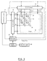
- Figures 3 and 4 show an equivalent circuit of an existing TFT-LCD.
- An input signal supplied to the existing TFT-LCD is described below by referring to Figures 3 and 4.
- a controller 31 converts image data into a form to be supplied to an X-driver 33 and a Y-driver 35 of a driver IC.
- an analog circuit 37 generates a voltage for each input signal.
- Input signals to be supplied to the TFT-LCD include a scanning signal (Vg) of a gate line 24 supplied from the Y-driver 35, a display signal (Vsig) of a data line 26 supplied from the X-driver 33, a common-electrode potential (Vcom) of a common electrode 30, and a storage capacitance line potential (Vcs) of a storage capacitance line 28.
- the potentials of these input signals are all supplied to the OLB electrode 60 extended from the pixel area in which the pixel electrodes 10 on the array substrate 12 are formed up to the perimeter of the area as shown in Figure 2. Then, among the potentials of these input signals, the potential Vcom is supplied to the common electrode 30 through the transfer 62.
- a liquid crystal display In general, a liquid crystal display must be inverted and driven by AC in order to prevent liquid crystal and alignment materials from deteriorating.
- the polarity inverting and driving method is classified as shown below. First, the method is classified into the following two methods because of the difference of the polarity inversion cycle of Vsig at the array substrate side: frame inversion (F inversion) and row inversion (H inversion). Among these methods, driving methods in which the polarities of adjacent display signals Vsig are opposite to each other are referred to as column inversion (V inversion) and dot inversion (H/V inversion).
- the polarity inversion cycle of the display signal Vsig is the same as the polarity inversion cycle of the pixel electrode potential.
- the polarity inversion cycle of the display signal Vsig is equal to or less than "1/(number of gate lines)" of the polarity inversion cycle of the pixel electrode potential.
- a driving method in which a polarity is inverted because the potential of a common electrode at the facing substrate side synchronizes with the display signal Vsig is referred to as common-voltage AC inversion driving (Vcom inversion) which is distinguished from a method in which common voltage is constant.
- Vcom inversion driving has an advantage that the maximum voltage amplitude of the display signal Vsig can be decreased because the voltage amplitude of the common electrode biased to the voltage amplitude of the display signal Vsig is applied to a liquid crystal layer. It is requested from the market of the TFT-LCD to lower the price of the TFT-LCD and increase the number of gradations of it.
- the TFT-LCD To lower the price of the TFT-LCD, it is effective to lower the price of a display-signal driver IC which is most frequently used among driving-circuit parts for driving the TFT-LCD in addition to the improvement of the yield and throughput in the manufacturing process. To lower the price of the IC, it is effective to use the Vcom inversion driving method making it possible to form a display-signal driver IC in a low-withstand-voltage process with a power supply voltage of 5 V or lower used for a general-purpose IC.
- the Vcom inversion driving is effective means to meet the market request for the TFT-LCD because it allows the number of gradations to easily increase.
- the problem of the signal delay of Vcom appears as a problem of the image quality such as irregularity of the display screen or decrease of the display contrast ratio in the case of a large high-definition TFT-LCD with a diagonal of 50 cm and display of approx. 1,000 rows.
- the problem of the signal delay of Vcom also occurs in a normal-size TFT-LCD.
- the transparent spherical spacers 36 (made of plastic and glass fibre) are hitherto scattered in the liquid crystal layer 34 held by the array substrate 12 and the facing substrate 14 constituting a liquid crystal display in order to keep the substrates 12 and 14 at a predetermined interval.
- liquid crystal flows in a panel when an external force is applied to the panel, the spacers are moved in a cell plane due to the flowing of the liquid crystal, and thereby the spacers may scratch the surface of the thin alignment film 54 due to the movement of the spacers.
- a cell gap (interval between electrodes of two substrates) may not be kept constant due to coagulation of the spacers.
- the optical path length difference (product of the birefringence rate and cell gap of the liquid crystal) of the liquid crystal layer changes and thereby, the contrast ratio and the chromaticity of a display screen are changed.
- problems occur that the uniformity of the screen cannot be kept or the display quality is deteriorated.
- the spacers are brightened or coagulated, and the light from the backlight 68 is cut off by the coagulated spacers and thereby the screen is blackened by the degree of cut-off light.
- the existing TFT-LCD has a problem in the structure of supplying the potential of the common electrode 30 on the facing substrate 14 from a plurality of portions at the perimeter of a pixel area of the array substrate 12 side to the common electrode 30 on the facing substrate 14 through the transfer 62 using conductive paste. Because this structure requires a high-accuracy alignment of the transfer 62, it uses two or more transfers to prevent defectives from being produced due to a deviation of a transfer. However, the manufacturing yield is decreased due to defectives produced in a process for dotting a transfer. Moreover, there is the restriction on design that an area for dotting a transfer must be formed at the perimeter of a pixel area. That is, because an area independent of display must exclusively be formed on the array substrate 12 and the facing substrate 14, an effective display area to a substrate size is decreased. However, it is inevitable to use the above structure because it is indispensable for an existing liquid crystal display in view of design.
- the present invention uses a pillar 78 of a colour filter 32 instead of a spacer in order to keep a cell gap between two substrates constant. Then, a signal delay of a common electrode 30 is prevented from occurring by forming a portion for electrically connecting a common electrode 30 covering the pillar 78 of the colour filter 32 with a storage capacitance line 28 everywhere in a pixel area and supplying a potential of the common electrode 30 from the storage capacitance line 28.
- the potential of the storage capacitance line 28 is supplied to the common electrode 30 on a facing substrate from joints formed everywhere in a pixel area.
- the common-electrode potential (Vcom) is frequently equalized with the storage capacitance line potential (Vcs) and the both potentials are supplied from the same supply source in most cases when going back to a driving circuit. Therefore, there is no problem in supplying Vcs as Vcom.
- a metal with a small electric resistance is generally used as the material of the line.
- this structure can be applied to TFT-LCDs other than a large or high-definition TFT-LCD and moreover applied to cases other than H/com inversion driving.
- the above structure is also designed so that a disconnected storage capacitance line which has been defective can be repaired because a potential can be supplied to the line from a common electrode.
- power consumption does not increase by using the above structure.
- the height of a pillar set on a facing substrate is kept at 5 ⁇ m or less, it is possible to prevent that a defective product is produced because a portion shaded by the pillar is not treated through rubbing and thereby causes incorrect orientation, even when using the pillar.
- a pillar of a colour filter on a facing substrate requires only change of mask patterns for the color filter but the number of processes does not increase. Moreover, it is possible to form a pillar by laminating red, green, and blue colour filters or any two colour filters of them. Furthermore, any sequence of colours to be laminated is not determined for a colour-filter laminating portion.
- a cell gap by forming a laminate structure containing a plurality of conductive materials at a position on an array substrate where a pillar is fitted on a facing substrate, connecting the laminate structure to a common electrode on the facing substrate through a conductive body layer electrically connected to a storage capacitance line, and specifying the cell gap by the sum of the height of the laminate structure on the array substrate and that of the pillar on the facing substrate.
- the alignment film is softer than a storage capacitance line material and a common electrode material, the alignment film is removed when the both materials contact each other and thereby, the both materials can electrically be connected.
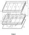
- the liquid crystal display panel 70 of the embodiments 1 to 3 of the present invention is described below by referring to Figures 6 to 11.
- the liquid crystal display panel 70 of these embodiments uses an active-matrix-driving liquid crystal display.
- the liquid crystal display panel 70 is provided with an array substrate 12 and a colour filter substrate 72 on which a colour filter 32 is formed as a facing substrate as shown in Figures 6 to 8.
- an undercoat layer 42, a gate electrode 20 (gate line 24), a pixel electrode 10, a gate insulating film 44, a semiconductor layer (channel layer) 46, a channel protective layer 48, an ohmic contact layer 50, a passivation film 52, and an alignment film 54 are formed in order on the array substrate 12.
- the undercoat layer 42, channel protective layer 48, passivation film 52, and alignment film 54 may not be formed.
- a TFT 16 is arranged near the intersection between the gate line 24 and the data line 26 and the gate electrode 20 of the TFT is formed by extending part of the gate line 24 and the drain electrode 22 of the TFT is formed by extending part of the data line 26.
- the source electrode 18 of the TFT is electrically connected to the pixel electrode 10.
- the embodiment 1 may have a structure in which the gate insulating film 44 is formed on the storage capacitance line 28 in a pixel area on the array substrate 12. That is, the embodiment 1 has a structure in which a hole 76 is formed at part of the gate insulating film 44 on the storage capacitance line 28, the common electrode 30 at a portion covering the pillar 78 of a colour filter formed on the colour filter substrate 72 is overlapped with the position of the hole 76, and the common electrode 30 contacts the storage capacitance line 28 so that they are electrically connected each other.
- the alignment film 54 may be formed on the whole surfaces of the pixel areas of the array substrate 12 and the colour filter substrate 72 at the contact plane between the line 28 and the substrate 72.
- the alignment film 54 covering the storage capacitance line 28 viewed through the hole 76 on the array substrate 12 with the common electrode 30 covering the pillar 78 on the colour filter substrate 72 when superimposing the array substrate 12 on the colour filter substrate 72 part of the alignment film 54 is shaved and the storage capacitance line 28 is electrically connected with the common electrode 30.
- the object of the present invention is achieved when only tens of portions are connected among millions of linkable portions. Therefore, there is no problem even if there are imperfectly-connected portions.
- the present invention does not require a spherical spacer for specifying a cell gap or transfer for supplying a potential to the common electrode 30 as shown in Figure 8.
- a spherical spacer for specifying a cell gap or transfer for supplying a potential to the common electrode 30 as shown in Figure 8.
- the equivalent circuit of the TFT-LCD of the present invention is shown in Figure 7 for comparison with the circuit in Figure 4.
- the advantages are obtained that the problem of signal delay of Vcom is solved because Vcom is equal to Vcs everywhere in a screen by applying the present invention and it is unnecessary to independently supply Vcom from the outside.
- the storage capacitance line 28 may be formed on the pixel electrode 10 formed on the array substrate 12 through the insulating film 74.
- a joint 80 between the storage capacitance line 28 and the common electrode 30 covering the pillar 78 of a colour filter is three-dimensionally superimposed on a storage capacitance area 82.
- a layer 84 made of a conductive body such as a metal formed simultaneously with the data line 26 is first formed on the storage capacitance line 28, and then it is connected with the common electrode 30 to constitute the joint 80 instead of directly connecting the common electrode 30 to the storage capacitance line 28 like the first and second embodiments. Therefore, it is possible to perform fine adjustment for realizing an optically-optimized cell gap by the formation of the conductive body.
- the undercoat layer 42 is formed on the array substrate 12.
- the gate electrode 20, gate line 24, and storage capacitance line 28 are formed on the undercoat layer 42.
- the gate insulating film 44 is formed.
- the semiconductor layer 46 of the TFT 16 is formed.
- the pixel electrode 10 is formed.
- the hole 76 is formed on part of the gate insulating film 44 on the storage capacitance line 28.
- the source electrode 18 and drain electrode 22 of the TFT 16 and the data line 26 are formed.
- the passivation film 52 covering the TFT 16 is formed.
- the alignment film 54 is formed and treated through rubbing.
- the colour filter 32 is formed on the facing substrate 14, and the pillar 78 of a colour filter is formed at a position corresponding to the hole 76 on the array substrate 12.
- the common electrode 30 is formed on the colour filter 32.
- the alignment film 54 is formed and treated through rubbing.
- the array substrate 12 and the colour filter substrate 72 finished through the above processes are made to face each other and the storage capacitance line 28 viewed through the hole 76 on the array substrate 12 is overlapped with the common electrode 30 at the portion covering the pillar 78 of a colour filter on the facing substrate 14 to electrically connect them each other.
- liquid crystal display panel 70 is finished by sealing the perimeter of the assembly with a sealant 64, injecting liquid crystal into the assembly through an injection hole (not illustrated), and closing the injection hole.
- the present invention provides a large high-definition liquid crystal display without causing a signal delay even around the central portion of a common electrode. Moreover, because the present invention disuses processes for scattering spacers and dotting transfers, the yield is improved and the cost is decreased.
Abstract
To prevent a signal delay of an active-matrix liquid crystal display from occurring.
In an active-matrix liquid crystal display having an active element for each pixel electrode, a potential is supplied to a common electrode (30) from a storage capacitance (28) line by forming a pillar (78) of a colour filter to specify a cell gap between an array substrate having the storage capacitance line and a facing substrate having the colour filter and electrically connecting the common electrode covering the pillar of the colour filter with the storage capacitance line on the array substrate.
Description
- The present invention relates to an active-matrix liquid crystal display. More particularly, the present invention relates to a thin-film-transistor liquid crystal display (TFT-LCD) having a storage capacitance line on an array substrate.
- A liquid crystal display (LCD) has been noticed in recent years as a display unit substituted for a CRT (Cathode Ray Tube) which is an existing display unit. This is first because the LCD has an advantage that the occupying area of it is smaller than that of the CRT since the LCD is a flat display unit. Therefore, the LCD makes it possible to decrease office spaces and the demand for the LCD is increased on and on as portable display and household displays become popular.
- Moreover, the LCD has an advantage that the power consumption is less than that of the CRT. Therefore, the LCD realizes a compact lightweight display provided with a small battery. In particular, an active-matrix liquid crystal display mounting an active element for each picture element of a liquid crystal display panel is noticed because it provides a display quality equal to that of the CRT.
- Figures 1 and 2 are a typical schematic and a sectional view showing the structure of an existing TFT-LCD. First, the structure of the existing TFT-LCD is described below by referring to Figure 1. The TFT-LCD comprises an
array substrate 12 on whichpixel electrodes 10 are formed like a matrix and a facingsubstrate 14 arranged so as to face the array substrate surface at a predetermined interval. ATFT 16 serving as a switching element is formed near thepixel electrodes 10 on thearray substrate 12 of the TFT-LCD respectively andsource electrodes 18 of these TFTs are connected to thepixel electrodes 10. Agate electrode 20 and adrain electrode 22 of a TFT are connected to thegate line 24 anddata line 26 constituting a row and a column of a matrix respectively. Thegate lines 24 and thedata lines 26 are formed at predetermined intervals and they are all perpendicular to each other. Moreover, eachpixel electrode 10 has a necessary capacitance between thepixel electrode 10 and thestorage capacitance line 28. This capacitance serves as astorage capacitance 29. - As shown in Figure 2, an existing TFT-LCD has a structure in which an
undercoat layer 42, a gate electrode 20 (gate line 24), apixel electrode 10, a gateinsulating film 44, a semiconductor layer (channel layer) 46, a channelprotective film 48, anohmic contact layer 50, apassivation film 52, and analignment film 54 are deposited on anarray substrate 12. Among these layers and films, theundercoat layer 42, channelprotective layer 48,passivation film 52, andalignment film 54 may not be deposited. Acommon electrode 30 is formed at the facingsubstrate 14 side of the TFT-LCD correspondingly to an area in whichpixel electrodes 10 on thearray substrate 12 are arranged like a matrix. Input signals are supplied to an OLB (Outer Lead Bonding)electrode 60 extended from a pixel area in which thepixel electrode 10 on thearray substrate 12 is formed up to the perimeter of the area. Among the potentials of these signals, the potential of thecommon electrode 30 on the facing substrate is supplied from a plurality of portions of electrodes on the array substrate through atransfer 62 using conductive paste at the outside of the pixel area. Thecommon electrode 30 is made of a transparent material such as ITO (Indium Tin Oxide) because it is necessary to pass light through theelectrode 30. However, because the material has a large electric resistance, the electric resistance from a potential supply terminal to the central portion of a display screen increases as a display unit increases in size. Moreover, in the case of a colour-display TFT-LCD, acolour filter 32 consisting of three primary colours of red (R), green (G), and blue (B) is formed like a matrix between the facingsubstrate 14 and thecommon electrode 30 correspondingly to thepixel electrode 10 of thearray substrate 12. Furthermore, ablack matrix 66 is formed like a lattice. In the case of an existing liquid crystal display, transparentspherical spacers 36 are scattered in aliquid crystal layer 34 held by thearray substrate 12 and the facingsubstrate 14 in order to keep a predetermined interval between the twosubstrates sealant 64. Furthermore, a polarizingfilm 38 is frequently set at the outer laterals of thearray substrate 12 and the facingsubstrate 14. Furthermore, a direct-view transmission-type TFT-LCD has abacklight 68 and an image is outputted by controlling the transmittance of anincident light 69 emitted from thebacklight 68. - Figures 3 and 4 show an equivalent circuit of an existing TFT-LCD. An input signal supplied to the existing TFT-LCD is described below by referring to Figures 3 and 4. A
controller 31 converts image data into a form to be supplied to anX-driver 33 and a Y-driver 35 of a driver IC. Moreover, ananalog circuit 37 generates a voltage for each input signal. Input signals to be supplied to the TFT-LCD include a scanning signal (Vg) of agate line 24 supplied from the Y-driver 35, a display signal (Vsig) of adata line 26 supplied from theX-driver 33, a common-electrode potential (Vcom) of acommon electrode 30, and a storage capacitance line potential (Vcs) of astorage capacitance line 28. The potentials of these input signals are all supplied to theOLB electrode 60 extended from the pixel area in which thepixel electrodes 10 on thearray substrate 12 are formed up to the perimeter of the area as shown in Figure 2. Then, among the potentials of these input signals, the potential Vcom is supplied to thecommon electrode 30 through thetransfer 62. - In general, a liquid crystal display must be inverted and driven by AC in order to prevent liquid crystal and alignment materials from deteriorating. In the case of a TFT-LCD, the polarity inverting and driving method is classified as shown below. First, the method is classified into the following two methods because of the difference of the polarity inversion cycle of Vsig at the array substrate side: frame inversion (F inversion) and row inversion (H inversion). Among these methods, driving methods in which the polarities of adjacent display signals Vsig are opposite to each other are referred to as column inversion (V inversion) and dot inversion (H/V inversion). In the case of the F inversion and V inversion, the polarity inversion cycle of the display signal Vsig is the same as the polarity inversion cycle of the pixel electrode potential. In the case of the H inversion and H/V inversion, however, the polarity inversion cycle of the display signal Vsig is equal to or less than "1/(number of gate lines)" of the polarity inversion cycle of the pixel electrode potential.
- A driving method in which a polarity is inverted because the potential of a common electrode at the facing substrate side synchronizes with the display signal Vsig is referred to as common-voltage AC inversion driving (Vcom inversion) which is distinguished from a method in which common voltage is constant. The Vcom inversion driving has an advantage that the maximum voltage amplitude of the display signal Vsig can be decreased because the voltage amplitude of the common electrode biased to the voltage amplitude of the display signal Vsig is applied to a liquid crystal layer. It is requested from the market of the TFT-LCD to lower the price of the TFT-LCD and increase the number of gradations of it. To lower the price of the TFT-LCD, it is effective to lower the price of a display-signal driver IC which is most frequently used among driving-circuit parts for driving the TFT-LCD in addition to the improvement of the yield and throughput in the manufacturing process. To lower the price of the IC, it is effective to use the Vcom inversion driving method making it possible to form a display-signal driver IC in a low-withstand-voltage process with a power supply voltage of 5 V or lower used for a general-purpose IC. The Vcom inversion driving is effective means to meet the market request for the TFT-LCD because it allows the number of gradations to easily increase.
- Because it is necessary to make the polarities of all the display signals Vsig written in the pixel electrodes same under the Vcom inversion driving, it is impossible to perform V inversion or H/V inversion of adjacent display signals Vsig with different polarities. Therefore, it is necessary to apply F inversion or H inversion to the display signals Vsig. However, under the F-inversion driving, many display irregularities of screen flickers or crosstalk are observed. Therefore, combination with H inversion is practical. In fact, a TFT-LCD using the driving method according to the combination of H inversion and Vcom inversion (H/com inversion) is widely marketed.
- In recent years, requests for increase in size and improvement in definition of a liquid crystal display have been strengthened according to increase of information content. However, the H/com inversion driving method is restricted in view of design for increase in size and improvement in definition of the liquid crystal display. It is inevitable to use a material with a high electric resistance such as ITO for the common electrode 30 (Figure 2) of a TFT-LCD because the electrode requires transparency. As a result, the electric resistance from a potential supply terminal to the central portion of a display screen according to increase of a display screen in size. Moreover, to improve the definition of the display screen of a TFT-LCD, it is necessary to increase the number of indicatable rows. However, because the polarity inversion cycle of Vcom synchronizes with the selection time of a scanning signal in the case of the H/com inversion driving, the potential fluctuation cycle of Vcom shortens by being inversely proportional to the number of scanning lines (= number of gate lines), that is, the number of indicatable rows of the display screen.
- Therefore, according to increase in size and improvement in definition of a TFT-LCD, the electric resistance of a common electrode increases and the potential fluctuation cycle of Vcom shortens. As a result, a problem occurs that a signal delay of Vcom happens, that is, Vcom cannot follow an input signal to be inputted to a common electrode around the central portion of a display screen. Figure 5 shows the state of the signal delay of Vcom. In this case, the polarity inversion cycle of Vcom at the time of H/com inversion is assumed as 1 H. The problem of the signal delay of Vcom appears as a problem of the image quality such as irregularity of the display screen or decrease of the display contrast ratio in the case of a large high-definition TFT-LCD with a diagonal of 50 cm and display of approx. 1,000 rows. The problem of the signal delay of Vcom also occurs in a normal-size TFT-LCD.
- Moreover, as shown in Figure 2, the transparent spherical spacers 36 (made of plastic and glass fibre) are hitherto scattered in the
liquid crystal layer 34 held by thearray substrate 12 and the facingsubstrate 14 constituting a liquid crystal display in order to keep thesubstrates thin alignment film 54 due to the movement of the spacers. Moreover, a cell gap (interval between electrodes of two substrates) may not be kept constant due to coagulation of the spacers. Unless the cell gap is kept constant, the optical path length difference (product of the birefringence rate and cell gap of the liquid crystal) of the liquid crystal layer changes and thereby, the contrast ratio and the chromaticity of a display screen are changed. Thus, problems occur that the uniformity of the screen cannot be kept or the display quality is deteriorated. Moreover, the spacers are brightened or coagulated, and the light from thebacklight 68 is cut off by the coagulated spacers and thereby the screen is blackened by the degree of cut-off light. To solve these problems, various structures are already disclosed which disuse transparent spherical spacers and instead, specify a cell gap by a pillar formed on thearray substrate 12 and/or the facing substrate 14 (official gazettes of Japanese Patent Laid-Open Nos. 164723/1985, 105583/1986, 24230/1989, 134733/1986, 163428/1992, 250416/1987, and 196946/1993). However, any one of these disclosures does not show means for solving the problem of signal delay in a TFT-LCD using the H/com inversion driving method. - Moreover, as shown in Figure 2, the existing TFT-LCD has a problem in the structure of supplying the potential of the
common electrode 30 on the facingsubstrate 14 from a plurality of portions at the perimeter of a pixel area of thearray substrate 12 side to thecommon electrode 30 on the facingsubstrate 14 through thetransfer 62 using conductive paste. Because this structure requires a high-accuracy alignment of thetransfer 62, it uses two or more transfers to prevent defectives from being produced due to a deviation of a transfer. However, the manufacturing yield is decreased due to defectives produced in a process for dotting a transfer. Moreover, there is the restriction on design that an area for dotting a transfer must be formed at the perimeter of a pixel area. That is, because an area independent of display must exclusively be formed on thearray substrate 12 and the facingsubstrate 14, an effective display area to a substrate size is decreased. However, it is inevitable to use the above structure because it is indispensable for an existing liquid crystal display in view of design. - It is an object of the present invention to overcome the above drawbacks.
- According to the present invention we provide a liquid crystal display as described in claim 9.
- Further according to the present invention we provide a liquid crystal display manufacturing method as described in claim ..
-
- Figure 1 shows the structure of an existing TFT-LCD (perspective view);
- Figure 2 shows the structure of the existing TFT-LCD (sectional view of the structure in Figure 1, taken along the line A-A of Figure 1);
- Figure 3 shows the equivalent circuit of the existing TFT-LCD;
- Figure 4 shows the equivalent circuit of the existing TFT-LCD (enlarged view);
- Figure 5 shows a signal delay of Vcom;
- Figure 6 shows the structure of the TFT-LCD of the present invention (perspective view);
- Figure 7 shows the equivalent circuit of the TFT-LCD of the present invention;
- Figure 8 shows the structure of the TFT-LCD described in the embodiment 1 of the present invention (sectional view of the structure in Figure 6, taken along the line B-B of Figure 6);
- Figure 9 shows an enlarged view of the picture-element section of the TFT-LCD described in the embodiment 1 of the present invention;
- Figure 10 shows an enlarged view of the picture-element section of the TFT-LCD described in the
embodiment 2 of the present invention; and - Figure 11 shows an enlarged view of the picture-element section of the TFT-LCD described in the third embodiment of the present invention.
- As shown in Figure 8, the present invention uses a
pillar 78 of acolour filter 32 instead of a spacer in order to keep a cell gap between two substrates constant. Then, a signal delay of acommon electrode 30 is prevented from occurring by forming a portion for electrically connecting acommon electrode 30 covering thepillar 78 of thecolour filter 32 with astorage capacitance line 28 everywhere in a pixel area and supplying a potential of thecommon electrode 30 from thestorage capacitance line 28. - According to the present invention, the potential of the
storage capacitance line 28 is supplied to thecommon electrode 30 on a facing substrate from joints formed everywhere in a pixel area. Originally, the common-electrode potential (Vcom) is frequently equalized with the storage capacitance line potential (Vcs) and the both potentials are supplied from the same supply source in most cases when going back to a driving circuit. Therefore, there is no problem in supplying Vcs as Vcom. Moreover, because transparency is not always requested for a material for forming a storage capacitance line, a metal with a small electric resistance is generally used as the material of the line. Therefore, by using the above structure, it is possible to supply the potential Vcom in which no signal delay occurs even around the central portion of a common electrode and prevent the existing problem on display characteristics caused by a signal delay of Vcom and due to increase in size and improvement in definition of a liquid crystal display. Moreover, this structure can be applied to TFT-LCDs other than a large or high-definition TFT-LCD and moreover applied to cases other than H/com inversion driving. - According to the above advantage, it is unnecessary to connect a storage capacitance line with a common electrode at every linkable portion and it is enough that the line and the electrode are connected at only tens of portions among millions of linkable portions. Therefore, by using the above structure, a defective due to stop of supply of a potential to be supplied to a common electrode does not occur. Moreover, it is possible to disuse a transfer set at the perimeter of a pixel area and a spherical spacer specifying a cell gap. Therefore, the productivity is improved, the number of restrictions on design is decreased, and display quality is improved. As for a transfer, because it is unnecessary that an area independent of display must hitherto be formed on an array substrate and a facing substrate and thereby an effective display area to a substrate size is decreased, it is possible to decrease the size of a liquid crystal display in the same pixel area.
- However, it is possible to set the transfer and spherical spacer as ever. Moreover, the above structure is also designed so that a disconnected storage capacitance line which has been defective can be repaired because a potential can be supplied to the line from a common electrode. However, power consumption does not increase by using the above structure. Moreover, when the height of a pillar set on a facing substrate is kept at 5 µm or less, it is possible to prevent that a defective product is produced because a portion shaded by the pillar is not treated through rubbing and thereby causes incorrect orientation, even when using the pillar.
- A pillar of a colour filter on a facing substrate requires only change of mask patterns for the color filter but the number of processes does not increase. Moreover, it is possible to form a pillar by laminating red, green, and blue colour filters or any two colour filters of them. Furthermore, any sequence of colours to be laminated is not determined for a colour-filter laminating portion. Furthermore, it is possible to fine-adjust a cell gap by forming a laminate structure containing a plurality of conductive materials at a position on an array substrate where a pillar is fitted on a facing substrate, connecting the laminate structure to a common electrode on the facing substrate through a conductive body layer electrically connected to a storage capacitance line, and specifying the cell gap by the sum of the height of the laminate structure on the array substrate and that of the pillar on the facing substrate.
- Furthermore, it is possible to use a structure for orienting liquid crystal by rubbing an alignment film used for many liquid crystal displays currently marketed. Because the alignment film is softer than a storage capacitance line material and a common electrode material, the alignment film is removed when the both materials contact each other and thereby, the both materials can electrically be connected.
- The liquid
crystal display panel 70 of the embodiments 1 to 3 of the present invention is described below by referring to Figures 6 to 11. The liquidcrystal display panel 70 of these embodiments uses an active-matrix-driving liquid crystal display. - In the case of the embodiment 1, the liquid
crystal display panel 70 is provided with anarray substrate 12 and acolour filter substrate 72 on which acolour filter 32 is formed as a facing substrate as shown in Figures 6 to 8. Moreover, as shown in Figure 8, anundercoat layer 42, a gate electrode 20 (gate line 24), apixel electrode 10, agate insulating film 44, a semiconductor layer (channel layer) 46, a channelprotective layer 48, anohmic contact layer 50, apassivation film 52, and analignment film 54 are formed in order on thearray substrate 12. Among these layers and films, theundercoat layer 42, channelprotective layer 48,passivation film 52, andalignment film 54 may not be formed. Moreover, as shown in Figure 9, aTFT 16 is arranged near the intersection between thegate line 24 and thedata line 26 and thegate electrode 20 of the TFT is formed by extending part of thegate line 24 and thedrain electrode 22 of the TFT is formed by extending part of thedata line 26. The source electrode 18 of the TFT is electrically connected to thepixel electrode 10. - Furthermore, as shown in Figure 8, the embodiment 1 may have a structure in which the
gate insulating film 44 is formed on thestorage capacitance line 28 in a pixel area on thearray substrate 12. That is, the embodiment 1 has a structure in which ahole 76 is formed at part of thegate insulating film 44 on thestorage capacitance line 28, thecommon electrode 30 at a portion covering thepillar 78 of a colour filter formed on thecolour filter substrate 72 is overlapped with the position of thehole 76, and thecommon electrode 30 contacts thestorage capacitance line 28 so that they are electrically connected each other. Though thestorage capacitance line 28 contacts thecommon electrode 30 on thecolour filter substrate 72 through thehole 76 of the gate insulating film, thealignment film 54 may be formed on the whole surfaces of the pixel areas of thearray substrate 12 and thecolour filter substrate 72 at the contact plane between theline 28 and thesubstrate 72. However, also in this case, by rubbing thealignment film 54 covering thestorage capacitance line 28 viewed through thehole 76 on thearray substrate 12 with thecommon electrode 30 covering thepillar 78 on thecolour filter substrate 72 when superimposing thearray substrate 12 on thecolour filter substrate 72, part of thealignment film 54 is shaved and thestorage capacitance line 28 is electrically connected with thecommon electrode 30. For this, the object of the present invention is achieved when only tens of portions are connected among millions of linkable portions. Therefore, there is no problem even if there are imperfectly-connected portions. - Moreover, the present invention does not require a spherical spacer for specifying a cell gap or transfer for supplying a potential to the
common electrode 30 as shown in Figure 8. However, there is no problem in using the spacer and transfer. The equivalent circuit of the TFT-LCD of the present invention is shown in Figure 7 for comparison with the circuit in Figure 4. As shown in Figure 7, the advantages are obtained that the problem of signal delay of Vcom is solved because Vcom is equal to Vcs everywhere in a screen by applying the present invention and it is unnecessary to independently supply Vcom from the outside. - As another method for connecting a common electrode with a storage capacitance line, the
storage capacitance line 28 may be formed on thepixel electrode 10 formed on thearray substrate 12 through the insulatingfilm 74. In this case, a joint 80 between thestorage capacitance line 28 and thecommon electrode 30 covering thepillar 78 of a colour filter is three-dimensionally superimposed on astorage capacitance area 82. - In the case of the third embodiment, a
layer 84 made of a conductive body such as a metal formed simultaneously with thedata line 26 is first formed on thestorage capacitance line 28, and then it is connected with thecommon electrode 30 to constitute the joint 80 instead of directly connecting thecommon electrode 30 to thestorage capacitance line 28 like the first and second embodiments. Therefore, it is possible to perform fine adjustment for realizing an optically-optimized cell gap by the formation of the conductive body. - Then, the process for manufacturing the liquid
crystal display panel 70 of this embodiment is described below. - First, the process for manufacturing the
array substrate 12 is described below. - In the first process, the
undercoat layer 42 is formed on thearray substrate 12. - In the second process, the
gate electrode 20,gate line 24, andstorage capacitance line 28 are formed on theundercoat layer 42. - In the third process, the
gate insulating film 44 is formed. - In the fourth process, the
semiconductor layer 46 of theTFT 16 is formed. - In the fifth process, the
pixel electrode 10 is formed. - In the sixth process, the
hole 76 is formed on part of thegate insulating film 44 on thestorage capacitance line 28. - In the seventh process, the
source electrode 18 anddrain electrode 22 of theTFT 16 and thedata line 26 are formed. - In the eighth process, the
passivation film 52 covering theTFT 16 is formed. - In the ninth process, the
alignment film 54 is formed and treated through rubbing. - Then, the method for manufacturing the
colour filter substrate 72 is described below. - In the first process, the
colour filter 32 is formed on the facingsubstrate 14, and thepillar 78 of a colour filter is formed at a position corresponding to thehole 76 on thearray substrate 12. - In the second process, the
common electrode 30 is formed on thecolour filter 32. - In the third process, the
alignment film 54 is formed and treated through rubbing. - The
array substrate 12 and thecolour filter substrate 72 finished through the above processes are made to face each other and thestorage capacitance line 28 viewed through thehole 76 on thearray substrate 12 is overlapped with thecommon electrode 30 at the portion covering thepillar 78 of a colour filter on the facingsubstrate 14 to electrically connect them each other. - Then, the liquid
crystal display panel 70 is finished by sealing the perimeter of the assembly with asealant 64, injecting liquid crystal into the assembly through an injection hole (not illustrated), and closing the injection hole. - The present invention provides a large high-definition liquid crystal display without causing a signal delay even around the central portion of a common electrode. Moreover, because the present invention disuses processes for scattering spacers and dotting transfers, the yield is improved and the cost is decreased.
Claims (10)
- A liquid crystal display panel comprising:an array substrate having pixel electrodes arranged like a matrix, an active element set to each of the pixel electrodes, a storage capacitance provided at some of the pixel electrodes, and a storage capacitance line for outputting the reference potential of the storage capacitance;a facing substrate having a plurality of pillars arranged so as to face the array substrate and formed higher than other portions specifying a cell gap together with objects formed on the array substrate and a common electrode covering at least some of the pillars, electrically connected to the storage capacitance line at the portions covering the pillars, and working on all pixels; anda liquid crystal layer held by the array substrate and the facing substrate.
- The liquid crystal display panel according to Claim 1, wherein the facing substrate has red, green, and blue colour filters formed correspondingly to the pixel electrodes and the pillars are made of colour-filter forming materials.
- The liquid crystal display panel according to Claim 2, wherein the pillars have a laminate structure of at least two colour materials of red, green, and blue colour-filter forming materials.
- The liquid crystal display panel according to any one of Claims 1 to 3, wherein the storage capacitance line has a laminate structure including a plurality of conductive materials electrically connected with the storage capacitance line each other at the joint between the storage capacitance line and the common electrode.
- A liquid crystal display of any preceding claim further comprising:
a polarizing film set at least either on the top of the facing substrate or on the bottom of the array substrate. - The liquid crystal display according to Claim 5, wherein a driver IC and a backlight for emitting light are included.
- A colour filter held by a facing substrate and a common electrode and having a plurality of pillars formed higher than other portions specifying a cell gap together with objects formed on an array substrate, wherein the pillars are covered with the common electrode.
- The colour filter according to Claim 7, wherein the pillars have a laminate structure made of at least two colour materials of red, green, and blue colour-filter forming materials.
- A liquid crystal display panel manufacturing method comprising the steps of:determining the height of a laminate structure including a storage capacitance line formed on an array substrate and a plurality of conductive materials electrically connected with the storage capacitance line each other and the height of a pillar of a colour filter formed on a colour filter substrate so that the sum of these heights specifies the distance between the array substrate and a facing substrate;forming the storage capacitance line and the laminate structure on the array substrate having pixel electrodes arranged like a matrix and active elements arranged in the vicinity of the pixel electrodes so that the storage capacitance line and the laminate structure have a determined height respectively;forming a colour filter at positions corresponding to the pixel electrodes on the colour filter substrate and also forming pillars of the plurality of colour filters so that the pillars have a determined height;superimposing the array substrate and the colour filter substrate so that the laminate structure and the pillar of the colour filter butt each other and sealing the circumferences of the superimposed array substrate and colour filter substrate; andinjecting liquid crystal between the array substrate and the colour filter substrate whose circumferences are sealed.
- The liquid crystal display panel manufacturing method according to Claim 9, wherein the plurality of pillars are formed with colour filter forming materials simultaneously with the colour filters.
Applications Claiming Priority (2)
| Application Number | Priority Date | Filing Date | Title |
|---|---|---|---|
| JP50749/95 | 1995-03-10 | ||
| JP5074995A JP3014291B2 (en) | 1995-03-10 | 1995-03-10 | Liquid crystal display panel, liquid crystal display device, and method of manufacturing liquid crystal display panel |
Publications (1)
| Publication Number | Publication Date |
|---|---|
| EP0731373A1 true EP0731373A1 (en) | 1996-09-11 |
Family
ID=12867493
Family Applications (1)
| Application Number | Title | Priority Date | Filing Date |
|---|---|---|---|
| EP96301290A Withdrawn EP0731373A1 (en) | 1995-03-10 | 1996-02-27 | Liquid crystal display |
Country Status (4)
| Country | Link |
|---|---|
| US (1) | US5748266A (en) |
| EP (1) | EP0731373A1 (en) |
| JP (1) | JP3014291B2 (en) |
| KR (1) | KR100236892B1 (en) |
Cited By (10)
| Publication number | Priority date | Publication date | Assignee | Title |
|---|---|---|---|---|
| FR2866722A1 (en) * | 2004-02-25 | 2005-08-26 | Lg Philips Lcd Co Ltd | Liquid crystal display device, for e.g. television, has projection formed at portion of column spacer to reduce contact surface between spacer and structures on substrates |
| WO2007002097A1 (en) * | 2005-06-22 | 2007-01-04 | Eastman Kodak Company | Oled device having spacers |
| DE10025261B4 (en) * | 1999-05-21 | 2008-07-24 | Lg. Philips Lcd Co., Ltd. | Liquid crystal display and method of making the same |
| CN101206356B (en) * | 2006-12-22 | 2010-12-29 | 群康科技(深圳)有限公司 | Liquid crystal display panel |
| CN101661183B (en) * | 2008-08-26 | 2011-02-16 | 株式会社日立显示器 | Liquid crystal display device |
| WO2013078697A1 (en) * | 2011-11-29 | 2013-06-06 | 深圳市华星光电技术有限公司 | Method for manufacturing color filter substrate, liquid crystal panel, and liquid crystal display device |
| CN103543564A (en) * | 2013-10-30 | 2014-01-29 | 深圳市华星光电技术有限公司 | Liquid crystal module, manufacturing method thereof and liquid crystal display device |
| CN103543897A (en) * | 2013-10-30 | 2014-01-29 | 深圳市华星光电技术有限公司 | Touch screen sensing device, manufacturing method of touch screen sensing device and touch screen sensing assembly |
| CN109839779A (en) * | 2017-11-29 | 2019-06-04 | 夏普株式会社 | Liquid crystal display panel |
| CN109891311A (en) * | 2016-09-05 | 2019-06-14 | 堺显示器制品株式会社 | The manufacturing method of display panel, display device and display panel |
Families Citing this family (85)
| Publication number | Priority date | Publication date | Assignee | Title |
|---|---|---|---|---|
| TW373098B (en) * | 1995-09-06 | 1999-11-01 | Toshiba Corp | Liquid crystal exposure component and its fabricating method |
| US6888608B2 (en) * | 1995-09-06 | 2005-05-03 | Kabushiki Kaisha Toshiba | Liquid crystal display device |
| US6320639B1 (en) * | 1996-03-11 | 2001-11-20 | Canon Kabushiki Kaisha | Liquid crystal device and process for production thereof |
| JP3949759B2 (en) * | 1996-10-29 | 2007-07-25 | 東芝電子エンジニアリング株式会社 | Color filter substrate and liquid crystal display element |
| JP3420675B2 (en) * | 1996-12-26 | 2003-06-30 | シャープ株式会社 | Liquid crystal display device and method of manufacturing the same |
| JP3883641B2 (en) * | 1997-03-27 | 2007-02-21 | 株式会社半導体エネルギー研究所 | Contact structure and active matrix display device |
| KR100242443B1 (en) * | 1997-06-16 | 2000-02-01 | 윤종용 | Liquid crystal panel for dot inversion driving and liquid crystal display device using the same |
| TW475087B (en) * | 1997-09-12 | 2002-02-01 | Toshiba Corp | Active matrix liquid crystal display device |
| TW535025B (en) * | 1998-12-03 | 2003-06-01 | Hitachi Ltd | Liquid crystal display device |
| JP2000305089A (en) | 1999-04-20 | 2000-11-02 | Nec Corp | Liquid crystal display device |
| US6275277B1 (en) * | 1999-05-17 | 2001-08-14 | Colorado Microdisplay, Inc. | Micro liquid crystal displays having a circular cover glass and a viewing area free of spacers |
| JP2000338523A (en) | 1999-05-25 | 2000-12-08 | Nec Corp | Liquid crystal display device |
| US6879391B1 (en) * | 1999-05-26 | 2005-04-12 | Kla-Tencor Technologies | Particle detection method and apparatus |
| US6504592B1 (en) | 1999-06-16 | 2003-01-07 | Nec Corporation | Liquid crystal display and method of manufacturing the same and method of driving the same |
| JP3285011B2 (en) | 1999-07-14 | 2002-05-27 | 日本電気株式会社 | Liquid crystal display |
| JP2001100217A (en) | 1999-09-29 | 2001-04-13 | Nec Corp | Color liquid crystal display device and method for manufacturing the same |
| US6493050B1 (en) * | 1999-10-26 | 2002-12-10 | International Business Machines Corporation | Wide viewing angle liquid crystal with ridge/slit pretilt, post spacer and dam structures and method for fabricating same |
| JP3713193B2 (en) * | 2000-01-18 | 2005-11-02 | シャープ株式会社 | Liquid crystal display device and manufacturing method thereof |
| TWI225557B (en) * | 2000-11-23 | 2004-12-21 | Au Optronics Corp | Manufacturing method of flat display device |
| KR100482469B1 (en) * | 2000-11-25 | 2005-04-14 | 비오이 하이디스 테크놀로지 주식회사 | Method for fabricating liquid crystal display for preventing cross talk |
| KR100721304B1 (en) * | 2000-12-29 | 2007-05-25 | 엘지.필립스 엘시디 주식회사 | Liquid Crystal Panel used for a Liquid Crystal Display Device and method for fabricating the same |
| KR100797374B1 (en) * | 2001-06-05 | 2008-01-22 | 엘지.필립스 엘시디 주식회사 | Liquid Crystal Display and Fabricating Method Thereof |
| JP4395612B2 (en) * | 2001-09-26 | 2010-01-13 | カシオ計算機株式会社 | Liquid crystal display element |
| KR100652048B1 (en) * | 2001-12-29 | 2006-11-30 | 엘지.필립스 엘시디 주식회사 | Liquid crystal display device |
| JP3992984B2 (en) * | 2002-01-04 | 2007-10-17 | シャープ株式会社 | LCD panel |
| KR100862535B1 (en) * | 2002-10-17 | 2008-10-09 | 엘지디스플레이 주식회사 | Liquid crystal display device using of column spacer and the fabrication method |
| JP2004198567A (en) * | 2002-12-17 | 2004-07-15 | Fujitsu Display Technologies Corp | Substrate for liquid crystal display device, and liquid crystal display device equipped with the same |
| JP4221704B2 (en) | 2003-03-17 | 2009-02-12 | 日本電気株式会社 | Liquid crystal display device and manufacturing method thereof |
| TW591287B (en) * | 2003-04-10 | 2004-06-11 | Au Optronics Corp | Liquid crystal display with an uniform common voltage and method thereof |
| KR101001963B1 (en) * | 2003-05-15 | 2010-12-17 | 삼성전자주식회사 | Liquid crystal display device |
| KR100489282B1 (en) * | 2003-06-17 | 2005-05-17 | 엘지.필립스 엘시디 주식회사 | Thin Film Transistor Array Substrate And Fabricating Method Thereof |
| US7011529B2 (en) * | 2004-03-01 | 2006-03-14 | Anritsu Company | Hermetic glass bead assembly having high frequency compensation |
| US20050255253A1 (en) * | 2004-05-13 | 2005-11-17 | White John M | Apparatus and methods for curing ink on a substrate using an electron beam |
| US20050253917A1 (en) * | 2004-05-13 | 2005-11-17 | Quanyuan Shang | Method for forming color filters in flat panel displays by inkjetting |
| TWI261716B (en) | 2004-05-13 | 2006-09-11 | Quanta Display Inc | Liquid crystal display apparatus and fabrication thereof |
| KR101133754B1 (en) * | 2004-08-19 | 2012-04-09 | 삼성전자주식회사 | Liquid crystal display device |
| US20060093751A1 (en) * | 2004-11-04 | 2006-05-04 | Applied Materials, Inc. | System and methods for inkjet printing for flat panel displays |
| US20060109296A1 (en) * | 2004-11-04 | 2006-05-25 | Bassam Shamoun | Methods and apparatus for inkjet printing color filters for displays |
| US20070042113A1 (en) * | 2004-11-04 | 2007-02-22 | Applied Materials, Inc. | Methods and apparatus for inkjet printing color filters for displays using pattern data |
| US20060092218A1 (en) * | 2004-11-04 | 2006-05-04 | Applied Materials, Inc. | Methods and apparatus for inkjet printing |
| US7413272B2 (en) * | 2004-11-04 | 2008-08-19 | Applied Materials, Inc. | Methods and apparatus for precision control of print head assemblies |
| US7625063B2 (en) * | 2004-11-04 | 2009-12-01 | Applied Materials, Inc. | Apparatus and methods for an inkjet head support having an inkjet head capable of independent lateral movement |
| US20060159843A1 (en) * | 2005-01-18 | 2006-07-20 | Applied Materials, Inc. | Method of substrate treatment for manufacturing of color filters by inkjet printing systems |
| CN100381924C (en) * | 2005-01-31 | 2008-04-16 | 友达光电股份有限公司 | Liquid crystal display device and manufacturing method thereof |
| US20060185587A1 (en) * | 2005-02-18 | 2006-08-24 | Applied Materials, Inc. | Methods and apparatus for reducing ink conglomerates during inkjet printing for flat panel display manufacturing |
| CN100464212C (en) * | 2005-04-08 | 2009-02-25 | 群康科技(深圳)有限公司 | Liquid crystal display and manufacturing method thereof |
| US7460267B2 (en) * | 2005-07-15 | 2008-12-02 | Applied Materials, Inc. | Green printing ink for color filter applications |
| US7544723B2 (en) * | 2005-07-15 | 2009-06-09 | Applied Materials, Inc. | Blue printing ink for color filter applications |
| KR20070011803A (en) * | 2005-07-21 | 2007-01-25 | 삼성에스디아이 주식회사 | Electron emission device, and flat display apparatus having the same |
| TWI318685B (en) * | 2005-07-28 | 2009-12-21 | Applied Materials Inc | Methods and apparatus for concurrent inkjet printing and defect inspection |
| US20070065571A1 (en) * | 2005-09-19 | 2007-03-22 | Applied Materials. Inc. | Method and apparatus for manufacturing a pixel matrix of a color filter for a flat panel display |
| US20070070132A1 (en) * | 2005-09-27 | 2007-03-29 | Fan-Cheung Sze | Inkjet delivery module |
| US7611217B2 (en) * | 2005-09-29 | 2009-11-03 | Applied Materials, Inc. | Methods and systems for inkjet drop positioning |
| US20070070109A1 (en) * | 2005-09-29 | 2007-03-29 | White John M | Methods and systems for calibration of inkjet drop positioning |
| US20070068560A1 (en) * | 2005-09-29 | 2007-03-29 | Quanyuan Shang | Methods and apparatus for inkjet print head cleaning |
| US20070076040A1 (en) * | 2005-09-29 | 2007-04-05 | Applied Materials, Inc. | Methods and apparatus for inkjet nozzle calibration |
| US20080018677A1 (en) * | 2005-09-29 | 2008-01-24 | White John M | Methods and apparatus for inkjet print head cleaning using an inflatable bladder |
| JP4940615B2 (en) * | 2005-09-30 | 2012-05-30 | カシオ計算機株式会社 | Liquid crystal display |
| TWI269075B (en) * | 2005-10-27 | 2006-12-21 | Chunghwa Picture Tubes Ltd | Manufacturing method of color filter device, liquid crystal display panel and manufacturing method thereof |
| KR20070074891A (en) * | 2006-01-11 | 2007-07-18 | 삼성전자주식회사 | Color filter substrate and liquid crystal display panel |
| US7554644B2 (en) * | 2006-01-27 | 2009-06-30 | Tpo Displays Corp. | LCD panel having capacitor disposed over or below photo spacer with active device also disposed between the photo spacer and a substrate, all disposed over opaque region of display |
| TWI328520B (en) * | 2006-02-07 | 2010-08-11 | Applied Materials Inc | Methods and apparatus for reducing irregularities in color filters |
| US20070252863A1 (en) * | 2006-04-29 | 2007-11-01 | Lizhong Sun | Methods and apparatus for maintaining inkjet print heads using parking structures with spray mechanisms |
| US20070263026A1 (en) * | 2006-04-29 | 2007-11-15 | Quanyuan Shang | Methods and apparatus for maintaining inkjet print heads using parking structures |
| US20070256709A1 (en) * | 2006-04-29 | 2007-11-08 | Quanyuan Shang | Methods and apparatus for operating an inkjet printing system |
| US7576815B2 (en) * | 2006-07-10 | 2009-08-18 | Intel Corporation | Method and apparatus of liquid-crystal-on-silicon assembly |
| US20080024532A1 (en) * | 2006-07-26 | 2008-01-31 | Si-Kyoung Kim | Methods and apparatus for inkjet printing system maintenance |
| WO2008013902A2 (en) * | 2006-07-28 | 2008-01-31 | Applied Materials, Inc. | Methods and apparatus for improved manufacturing of color filters |
| KR101299646B1 (en) * | 2006-10-12 | 2013-08-26 | 삼성디스플레이 주식회사 | Display panel and method of manufacturing the same |
| US20080204501A1 (en) * | 2006-12-01 | 2008-08-28 | Shinichi Kurita | Inkjet print head pressure regulator |
| US7857413B2 (en) | 2007-03-01 | 2010-12-28 | Applied Materials, Inc. | Systems and methods for controlling and testing jetting stability in inkjet print heads |
| JP2008275908A (en) * | 2007-04-27 | 2008-11-13 | Nec Lcd Technologies Ltd | Liquid crystal panel and liquid crystal display device using it |
| WO2008152864A1 (en) * | 2007-06-11 | 2008-12-18 | Sharp Kabushiki Kaisha | Method of manufacturing color filter substrate, method of manufacturing liquid crystal display device, color filter substrate, and liquid crystal display device |
| US7812918B2 (en) * | 2007-07-12 | 2010-10-12 | Lg Display Co., Ltd. | Liquid crystal display device and method for fabricating the same |
| US7637587B2 (en) * | 2007-08-29 | 2009-12-29 | Applied Materials, Inc. | System and method for reliability testing and troubleshooting inkjet printers |
| US20090141218A1 (en) * | 2007-10-26 | 2009-06-04 | Applied Materials, Inc. | Methods and apparatus for curing pixel matrix filter materials |
| JP2009204724A (en) | 2008-02-26 | 2009-09-10 | Toshiba Mobile Display Co Ltd | Display element |
| TWI382381B (en) * | 2008-03-06 | 2013-01-11 | Pervasive Display Co Ltd | Non-volatile type display apparatus |
| US20120013839A1 (en) * | 2009-03-27 | 2012-01-19 | Sharp Kabushiki Kaisha | Display panel and display device |
| JP5866997B2 (en) * | 2011-11-17 | 2016-02-24 | 凸版印刷株式会社 | Photomask and color filter manufacturing method |
| KR101985481B1 (en) * | 2012-07-23 | 2019-06-05 | 삼성디스플레이 주식회사 | Display device and method of manufacturing the same |
| TWI490618B (en) | 2013-01-04 | 2015-07-01 | E Ink Holdings Inc | Pixel structure |
| JP2016099492A (en) | 2014-11-21 | 2016-05-30 | セイコーエプソン株式会社 | Liquid crystal device and electronic apparatus |
| CN104765201A (en) * | 2015-03-30 | 2015-07-08 | 深圳市华星光电技术有限公司 | Liquid crystal display device and liquid crystal display panel thereof |
| CN113419385B (en) * | 2021-05-31 | 2022-09-27 | 北海惠科光电技术有限公司 | Display panel, preparation method thereof and display device |
Citations (4)
| Publication number | Priority date | Publication date | Assignee | Title |
|---|---|---|---|---|
| DE3524086A1 (en) * | 1985-07-05 | 1987-01-08 | Vdo Schindling | LIQUID CRYSTAL CELL |
| US4961630A (en) * | 1989-03-15 | 1990-10-09 | Ovonic Imaging Systems, Inc. | Liquid crystal display with auxiliary pixel capacitance interconnected through substrate |
| JPH03196020A (en) * | 1989-12-25 | 1991-08-27 | Casio Comput Co Ltd | Liquid crystal display device |
| JPH0493924A (en) * | 1990-08-07 | 1992-03-26 | Sony Corp | Liquid crystal display device |
Family Cites Families (7)
| Publication number | Priority date | Publication date | Assignee | Title |
|---|---|---|---|---|
| DE3153620C2 (en) * | 1980-04-01 | 1992-01-23 | Canon K.K., Tokio/Tokyo, Jp | |
| FR2614718B1 (en) * | 1987-04-28 | 1989-06-16 | Commissariat Energie Atomique | MATRIX DISPLAY WITH LIQUID CRYSTALS PROVIDED WITH STORAGE CAPACITIES |
| JPS64930A (en) * | 1987-06-24 | 1989-01-05 | Alps Electric Co Ltd | Liquid crystal element |
| JP2605723B2 (en) * | 1987-07-22 | 1997-04-30 | 日本電気株式会社 | Thin film transistor array type liquid crystal display |
| ATE142352T1 (en) * | 1990-05-31 | 1996-09-15 | Canon Kk | LIQUID CRYSTAL COLOR DISPLAY AND METHOD FOR PRODUCING SAME |
| KR930002855A (en) * | 1991-07-15 | 1993-02-23 | 이헌조 | Manufacturing method of liquid crystal display device |
| JPH05249478A (en) * | 1991-12-25 | 1993-09-28 | Toshiba Corp | Liquid crystal display device |
-
1995
- 1995-03-10 JP JP5074995A patent/JP3014291B2/en not_active Expired - Lifetime
-
1996
- 1996-02-23 KR KR1019960005181A patent/KR100236892B1/en not_active IP Right Cessation
- 1996-02-27 EP EP96301290A patent/EP0731373A1/en not_active Withdrawn
- 1996-03-11 US US08/615,012 patent/US5748266A/en not_active Expired - Lifetime
Patent Citations (4)
| Publication number | Priority date | Publication date | Assignee | Title |
|---|---|---|---|---|
| DE3524086A1 (en) * | 1985-07-05 | 1987-01-08 | Vdo Schindling | LIQUID CRYSTAL CELL |
| US4961630A (en) * | 1989-03-15 | 1990-10-09 | Ovonic Imaging Systems, Inc. | Liquid crystal display with auxiliary pixel capacitance interconnected through substrate |
| JPH03196020A (en) * | 1989-12-25 | 1991-08-27 | Casio Comput Co Ltd | Liquid crystal display device |
| JPH0493924A (en) * | 1990-08-07 | 1992-03-26 | Sony Corp | Liquid crystal display device |
Non-Patent Citations (2)
| Title |
|---|
| PATENT ABSTRACTS OF JAPAN vol. 015, no. 460 (P - 1278) 21 November 1991 (1991-11-21) * |
| PATENT ABSTRACTS OF JAPAN vol. 016, no. 319 (P - 1385) 13 July 1992 (1992-07-13) * |
Cited By (13)
| Publication number | Priority date | Publication date | Assignee | Title |
|---|---|---|---|---|
| US8184254B2 (en) | 1999-05-21 | 2012-05-22 | Lg Display Co., Ltd. | Liquid crystal display and fabrication method thereof |
| DE10025261B4 (en) * | 1999-05-21 | 2008-07-24 | Lg. Philips Lcd Co., Ltd. | Liquid crystal display and method of making the same |
| US7889306B1 (en) | 1999-05-21 | 2011-02-15 | Lg Display Co., Ltd. | Liquid crystal display and fabrication method thereof |
| FR2866722A1 (en) * | 2004-02-25 | 2005-08-26 | Lg Philips Lcd Co Ltd | Liquid crystal display device, for e.g. television, has projection formed at portion of column spacer to reduce contact surface between spacer and structures on substrates |
| WO2007002097A1 (en) * | 2005-06-22 | 2007-01-04 | Eastman Kodak Company | Oled device having spacers |
| CN101206356B (en) * | 2006-12-22 | 2010-12-29 | 群康科技(深圳)有限公司 | Liquid crystal display panel |
| CN101661183B (en) * | 2008-08-26 | 2011-02-16 | 株式会社日立显示器 | Liquid crystal display device |
| WO2013078697A1 (en) * | 2011-11-29 | 2013-06-06 | 深圳市华星光电技术有限公司 | Method for manufacturing color filter substrate, liquid crystal panel, and liquid crystal display device |
| CN103543564A (en) * | 2013-10-30 | 2014-01-29 | 深圳市华星光电技术有限公司 | Liquid crystal module, manufacturing method thereof and liquid crystal display device |
| CN103543897A (en) * | 2013-10-30 | 2014-01-29 | 深圳市华星光电技术有限公司 | Touch screen sensing device, manufacturing method of touch screen sensing device and touch screen sensing assembly |
| CN103543897B (en) * | 2013-10-30 | 2017-02-08 | 深圳市华星光电技术有限公司 | Touch screen sensing device, manufacturing method of touch screen sensing device and touch screen sensing assembly |
| CN109891311A (en) * | 2016-09-05 | 2019-06-14 | 堺显示器制品株式会社 | The manufacturing method of display panel, display device and display panel |
| CN109839779A (en) * | 2017-11-29 | 2019-06-04 | 夏普株式会社 | Liquid crystal display panel |
Also Published As
| Publication number | Publication date |
|---|---|
| KR960035101A (en) | 1996-10-24 |
| JPH08262484A (en) | 1996-10-11 |
| US5748266A (en) | 1998-05-05 |
| KR100236892B1 (en) | 2000-01-15 |
| JP3014291B2 (en) | 2000-02-28 |
Similar Documents
| Publication | Publication Date | Title |
|---|---|---|
| US5748266A (en) | Color filter, liquid crystal display panel, liquid crystal display, and liquid crystal display panel manufacturing method | |
| CN100445845C (en) | Liquid crystal display device having an injection hole for liquid crystal | |
| US6603525B2 (en) | Liquid crystal display | |
| US7057698B2 (en) | Liquid crystal display panel of horizontal electric field applying type including plurality of pixels divided into at least four sub-pixels | |
| US5854616A (en) | Active matrix type liquid crystal display system and driving method therefor | |
| US6667790B2 (en) | Liquid crystal display having particular spacer | |
| US6400428B1 (en) | Liquid crystal device/display utilizing a plurality of adjoining display panels to form single display screen and methods related thereto | |
| US6762819B2 (en) | Liquid crystal display device with electrodes on barrier ribs and fabricating method thereof | |
| CN100386675C (en) | Liquid crystal display | |
| US7298448B2 (en) | Liquid crystal display with a uniform common voltage and method thereof | |
| US6181405B1 (en) | Large screen display device with a plurality of independently sealed and interconnected substrates | |
| KR101157975B1 (en) | Method For Driving Liquid Crystal Display Device | |
| JPH08254712A (en) | Liquid crystal display element | |
| US20040125256A1 (en) | Liquid crystal display device | |
| JP2008275908A (en) | Liquid crystal panel and liquid crystal display device using it | |
| CN110703515A (en) | Display panel and manufacturing method thereof | |
| JPS61282823A (en) | Liquid crystal panel for color television | |
| US6198464B1 (en) | Active matrix type liquid crystal display system and driving method therefor | |
| KR20080059928A (en) | Liquid crystal display device and method for repairing the same | |
| CN109283761B (en) | Display panel, manufacturing method of display panel and display device | |
| KR20010072902A (en) | Liquid crystal display, method for driving the same, and method for manufacturing the same | |
| KR100579190B1 (en) | Liquid Crystal Display | |
| KR100560788B1 (en) | Liquid Crystal Display | |
| CN219267288U (en) | Narrow frame array substrate and GOA panel | |
| KR20040017638A (en) | Array Substrate in Liquid Crystal Display Device |
Legal Events
| Date | Code | Title | Description |
|---|---|---|---|
| PUAI | Public reference made under article 153(3) epc to a published international application that has entered the european phase |
Free format text: ORIGINAL CODE: 0009012 |
|
| AK | Designated contracting states |
Kind code of ref document: A1 Designated state(s): DE FR GB |
|
| STAA | Information on the status of an ep patent application or granted ep patent |
Free format text: STATUS: THE APPLICATION IS DEEMED TO BE WITHDRAWN |
|
| 18D | Application deemed to be withdrawn |
Effective date: 19970312 |