EP0734047A2 - Plasma processing method and apparatus - Google Patents
Plasma processing method and apparatus Download PDFInfo
- Publication number
- EP0734047A2 EP0734047A2 EP96301870A EP96301870A EP0734047A2 EP 0734047 A2 EP0734047 A2 EP 0734047A2 EP 96301870 A EP96301870 A EP 96301870A EP 96301870 A EP96301870 A EP 96301870A EP 0734047 A2 EP0734047 A2 EP 0734047A2
- Authority
- EP
- European Patent Office
- Prior art keywords
- plasma
- specimen
- temperature
- generation chamber
- plasma generation
- Prior art date
- Legal status (The legal status is an assumption and is not a legal conclusion. Google has not performed a legal analysis and makes no representation as to the accuracy of the status listed.)
- Withdrawn
Links
Images


Classifications
-
- H—ELECTRICITY
- H01—ELECTRIC ELEMENTS
- H01L—SEMICONDUCTOR DEVICES NOT COVERED BY CLASS H10
- H01L21/00—Processes or apparatus adapted for the manufacture or treatment of semiconductor or solid state devices or of parts thereof
- H01L21/02—Manufacture or treatment of semiconductor devices or of parts thereof
- H01L21/04—Manufacture or treatment of semiconductor devices or of parts thereof the devices having at least one potential-jump barrier or surface barrier, e.g. PN junction, depletion layer or carrier concentration layer
- H01L21/18—Manufacture or treatment of semiconductor devices or of parts thereof the devices having at least one potential-jump barrier or surface barrier, e.g. PN junction, depletion layer or carrier concentration layer the devices having semiconductor bodies comprising elements of Group IV of the Periodic System or AIIIBV compounds with or without impurities, e.g. doping materials
- H01L21/30—Treatment of semiconductor bodies using processes or apparatus not provided for in groups H01L21/20 - H01L21/26
- H01L21/302—Treatment of semiconductor bodies using processes or apparatus not provided for in groups H01L21/20 - H01L21/26 to change their surface-physical characteristics or shape, e.g. etching, polishing, cutting
- H01L21/306—Chemical or electrical treatment, e.g. electrolytic etching
- H01L21/3065—Plasma etching; Reactive-ion etching
-
- H—ELECTRICITY
- H01—ELECTRIC ELEMENTS
- H01J—ELECTRIC DISCHARGE TUBES OR DISCHARGE LAMPS
- H01J37/00—Discharge tubes with provision for introducing objects or material to be exposed to the discharge, e.g. for the purpose of examination or processing thereof
- H01J37/32—Gas-filled discharge tubes
- H01J37/32431—Constructional details of the reactor
- H01J37/32458—Vessel
- H01J37/32477—Vessel characterised by the means for protecting vessels or internal parts, e.g. coatings
- H01J37/32504—Means for preventing sputtering of the vessel
-
- H—ELECTRICITY
- H01—ELECTRIC ELEMENTS
- H01J—ELECTRIC DISCHARGE TUBES OR DISCHARGE LAMPS
- H01J37/00—Discharge tubes with provision for introducing objects or material to be exposed to the discharge, e.g. for the purpose of examination or processing thereof
- H01J37/32—Gas-filled discharge tubes
- H01J37/32431—Constructional details of the reactor
- H01J37/32458—Vessel
- H01J37/32522—Temperature
-
- H—ELECTRICITY
- H01—ELECTRIC ELEMENTS
- H01J—ELECTRIC DISCHARGE TUBES OR DISCHARGE LAMPS
- H01J2237/00—Discharge tubes exposing object to beam, e.g. for analysis treatment, etching, imaging
- H01J2237/02—Details
- H01J2237/022—Avoiding or removing foreign or contaminating particles, debris or deposits on sample or tube
Definitions
- the present invention relates to a plasma processing method and apparatus and more specifically to a plasma processing method and apparatus suited for plasma-processing specimens such as semiconductor device substrates.
- reaction products also adhere to the lower part of the specimen mount, the inner bottom portion of the processing chamber and the exhaust pipe. During the plasma processing, these reaction products are not only deposited on these portions but also flake off contaminating the specimens, greatly reducing the yield of specimens.
- the object of this invention is to solve such problems.
- the invention provides a plasma processing method and apparatus, which controls the temperature of locations where reaction products or gaseous reaction products (hereinafter referred to as reaction products) adhere thereby preventing abnormal generation of reaction products and ensuring high yield of specimens.
- the locations above the specimen are controlled at temperatures at which the reaction products do not solidify and the locations below the specimen (lower part of the specimen mount, inner bottom portion of the processing chamber, exhaust pipe, etc.) are controlled at temperatures at which the reaction products solidify.
- the portions, above the specimen, of the inner side surface of the processing chamber where plasma is generated are set at temperatures at which reaction products sublimate, while the lower part of the specimen mount, the inner bottom portion of the processing chamber and the exhaust pipe are set at temperatures at which the reaction products solidify.
- Reaction products and foreign matters floating in the processing chamber adhere to or are trapped by the lower portion of the specimen mount, the inner bottom portion in the processing chamber and the exhaust pipe. While the vacuum is maintained, foreign matters can be prevented from being flaked off and the flaked matters from floating around because these locations are controlled at all times at temperatures at which reaction products solidify.
- Figure 1 is a vertical cross section showing a microwave plasma processing apparatus as one embodiment of this invention.
- Figure 2 is a vapor pressure curve diagram for etching gases and reaction products as one embodiment of this invention.
- FIG. 3 is a control sequence diagram for the plasma processing apparatus as one embodiment of this invention.
- Figure 4 is a vertical cross section showing a parallel plate type plasma etching apparatus as another embodiment of this invention.
- Figure 5 is a vertical cross section showing an induction coupled discharge type apparatus as still another embodiment of this invention.
- Figure 6 is a vertical cross section showing a parallel plate type plasma etching apparatus as a further embodiment of this invention.
- Figure 7 is a vertical cross section showing a microwave discharge type apparatus as a further embodiment of this invention.
- Figure 1 is a vertical cross section of an essential portion of the microwave plasma processing apparatus showing its outline configuration as one embodiment of this invention.
- a processing chamber 10 has a quartz discharge tube 14 as its upper constitutional element.
- the processing chamber 10 is provided with a gas supply port 15 connected to a gas source (not shown) for supplying an etching gas to the processing chamber 10, and also with an exhaust port 16 leading to a vacuum discharge apparatus (not shown).
- a specimen mount 11 on which to place a semiconductor device substrate (wafer) 13.
- the specimen mount 11 is connected to a high frequency power source 12 so that a high frequency power can be applied to the specimen mount 11.
- the discharge tube 14 is enclosed by a waveguide 17, on the outer side of which there is provided a solenoid coil 19 that produces a magnetic field in the discharge tube 14.
- the discharge tube 14 in the processing chamber 10 is provided with a temperature controller I 34.
- the waveguide 17 is provided at its end with a magnetron 18 that oscillates microwaves.
- a lower part of the specimen mount, the inner bottom portion of the chamber and the exhaust pipe in the processing chamber 10 are also provided with a temperature controller II 35.
- the temperature controllers I34, II35 control the temperature of the inner sidewall of the processing chamber at a desired temperature according to temperature sensors 36, 37 fitted to the inner sidewall of the processing chamber or installed in the sidewall. It is also possible to set a plurality of locations for temperature control, i.e., for heating and cooling.
- a processing gas for etching is supplied from the gas supply port 15 into the processing chamber 10 and at the same time the processing chamber 10 is evacuated to a specified pressure. Then, microwaves are introduced into the discharge tube 14 from the magnetron 18 through the waveguide 17, and the solenoid coil 19 generates a magnetic field to plasmatize the processing gas in the discharge tube 14 by the interaction between the electric field of the microwaves and the magnetic field of the solenoid coil 19.
- the high frequency power source 12 applies a high frequency power to the specimen mount 11 to produce a bias voltage and thereby draw ions in the plasma toward the wafer 13 to perform anisotropic etching on the wafer 13. At this time, the reaction products produced by etching are discharged from the sidewall and lower part of the specimen mount and from the inner bottom of the processing chamber through the exhaust pipe.
- the temperature control regions for the temperature controllers I34, II35 are shown in Table 1.
- Table 1 the inner sidewall portion corresponding to the plasma generation region in the processing chamber 10 is controlled at an elevated temperature range of 100°C and more than 100°C to 400°C and other portions, such as side surface and lower part of the specimen mount, the inner bottom portion of the processing chamber and the exhaust pipe, are cooled at -200°C or more than -200°C to less than 100°C.
- the reason why cooling temperature is set at more than -200°C or -200°C is based on the tool to cool the lower part of the chamber. Liquid nitrogen is practically available and it can cool at about -200°C, so the cooling lowest limit is decided.
- Figure 2 shows an example vapor pressure curve for the etching gas and reaction products in the case of aluminum wiring material.
- reaction product AlCl 3 solidifies at 100 °C when the etching pressure is 1 Torr. That is, it is seen that reaction products are deposited when the inner sidewall of the processing chamber of the plasma processing apparatus of Figure 1 is lower than 100°C.
- the plasma processing is performed continuously under this condition, deposits flake off as foreign matters in the processing chamber.
- the inner sidewall of the processing chamber at 100°C or more than 100°C and the lower part of the specimen mount, the inner bottom portion of the processing chamber and the exhaust pipe at lower than 100°C, it is possible to prevent the reaction products from adhering to the inner sidewall of the processing chamber and cause the reaction products to selectively adhere to the lower part of the specimen mount, the inner bottom of the processing chamber and the exhaust pipe, thereby minimizing foreign matters falling onto the surface of the wafer being etched or those floating from the inner bottom of the processing chamber.
- the similar effect is also obtained by putting under appropriate temperature conditions the processing chamber, the sidewall and lower part of the specimen mount, the inner bottom portion of the processing chamber and the exhaust pipe.
- FIG. 3 shows the control sequence for the plasma processing apparatus of Figure 1.
- the temperature controller I 34 controls the temperature of the inner sidewall of the processing chamber and the temperature controller II 35 controls the temperature of the side surface and lower part of the specimen mount, the inner bottom portion of the processing chamber and the exhaust pipe.
- the normal etching sequence is performed.
- the temperature controllers I34, II 35 are turned off and the apparatus is opened to air for normal cleaning.
- the processing chamber 10 is heated to a predetermined temperature where it is controlled to be maintained.
- the temperature controller II 35 is started, the lower portion of the specimen mount 11, the inner bottom portion of the processing chamber 10 and the exhaust pipe are cooled to the predetermined temperature where they are controlled to be maintained.
- the wafer 13, in this case, one, is carried into the processing chamber 10 by a wafer carrying device not shown.
- the wafer 13 is transferred from the wafer carrying device onto the surface of the specimen mount, with the surface of the wafer to be etched facing up.
- the wafer 13 thus mounted on the specimen mount 11 is held immovable.
- the processing chamber 10 is evacuated.
- the gases in the processing chamber 10 are discharged through the exhaust pipe fitted with an exhaust valve and a variable resistance valve (not shown).
- the pressure in the processing chamber 10 being evacuated is reduced to a specified pressure by adjusting the variable resistance valve.
- the etching gas is supplied from the gas supply source through the gas supply port 15 into the processing chamber 10.
- the amount of etching gas supplied to the processing chamber 10 is controlled at a predetermined value by a gas flow controller (not shown).
- a part of the etching gas supplied into the processing chamber 10 is discharged out of the processing chamber 10 by the evacuation device to control the pressure in the processing chamber 10 at a specified etching processing pressure.
- the magnetron 18 and the solenoid coil 19 are operated to plasmatize the etching gas in the processing chamber 10.
- the etching surface of the wafer 13 held on the specimen mount 11 is processed by the plasma.
- the high frequency power source 12 is operated to apply the high frequency power to the specimen mount 11, thereby applying a bias to the wafer 13. With the bias applied, the etching surface of the wafer 13 is etched.
- the supply of etching gas to the processing chamber 10 and the operation of the high frequency power source 12, magnetron 18 and solenoid coil 19 are stopped.
- the processed wafer 13 is transferred from the specimen mount 11 to the wafer carrying device, which takes it out of the processing chamber 10.
- a new wafer 13 is placed into the processing chamber 10 by the wafer carrying device, and the above-mentioned processing is performed.
- the temperature controllers I34, II 35 continue their operation to keep the temperatures of various portions of the apparatus at the controlled temperatures. In some cases, the operation of the temperature controllers I34, II 35, may be stopped between the wafer processing.
- the apparatus is stopped when the wafer processing is interrupted for an extended period of time because of failure or for some other reasons, or when the work for the day has been finished.
- the operation of the temperature controllers I 34, II 35 is also stopped when the interior of the processing chamber 10 is opened to air for cleaning. Particularly by stopping the operation of the temperature controller II 35, it is possible to prevent impurities such as water contained in air from adhering to the cooled portions when the processing chamber 10 is opened to air. In this way, the inconveniences experienced at time of evacuation of the processing chamber 10 (prolonged evacuation time and failure to reach a specified pressure) can be eliminated.
- control temperatures of various portions controlled by the temperature controllers I 34, II 35 depend on the film quality of the wafer 13, i.e., wiring material and the kind of etching gas.
- Information on the wafer 13 to be etched such as wiring material and the kind of etching gas compatible with the wiring material, is entered into the higher level controller (not shown) by an operator.
- the higher level controller then outputs control signalsto the temperature controllers I 34, II 35, which in turn control the temperatures of various portions.
- Such a temperature control is performed by an operator entering the information on the wafer 13 through a touch panel or by reading the wafer information by some means into the higher level controller or directly into the temperature controllers I 34, II 35.
- the temperatures of various portions can be controlled reliably at specified temperatures, thereby improving the wafer yield stably and reliably.
- the reaction products are made to adhere to the cooled portions, forming deposits there.
- the maintenance is performed before or when the deposit thickness reaches a point that causes an increase in exhaust resistance or produces foreign matters by deposit flaking.
- the cooling of the cooled portions by the temperature controller II 35 is stopped.
- the cooled portions are then heated to the sublimation temperature of the deposit.
- the deposit adhering to the cooled portion is sublimated and discharged out of the processing chamber 10 by operating the evacuation device.
- the heating of the cooled portions is stopped and the temperature control by the temperature controller II 35 is performed.
- the heating of the cooled portions may be realized by adding a heating device (not shown) or by constructing the temperature controller II 35 to have the cooling and heating functions and switching between the functions.
- the maintenance of the cooled portions is done before opening the processing chamber 10 to air.
- the cleaning is done by plasma without opening the processing chamber 10 to air, the maintenance is performed before or during cleaning.
- This embodiment offers the following advantages.
- the coolingof the inner bottom portion of the processing chamber educes the temperature of the inner sidewall portion of the processing chamber below the evaporation point of reaction products, the reaction products and floating foreign matters adhere to or become deposited on the inner sidewall portion of the processing chamber.
- the inner sidewall portion of the processing chamber is located higher than the etching surface of the water being processed, the adhesion and deposition of reaction products to the inner sidewall portion are very disadvantageous in terms of wafer yield. That is, the deposit may flake off the inner sidewall portion of the processing clamber and fall as foreign matters onto the wafer being processed, lowering the yield.
- the embodiment of this invention heats the inner sidewall portion of the processing chamber to a temperature at which reaction products will not adhere to it and, at the same time, cools the lower part of the specimen mount, the inner bottom portion of the processing chamber and the exhaust pipe to a temperature at which the reaction products easily adhere to them. This prevents foreign matters from being formed, thus improving the wafer yield.
- this embodiment is characterized by the concept that the adhesion of reaction products to the inner sidewall portion of the processing chamber located higher than the etching surface of the wafer being processed is minimized while at the same time the reaction products and floating foreign matters are positively induced to adhere to the lower part of the specimen mount, the inner bottom portion of the processing chamber and the exhaust pipe, all located below the etching surface of the wafer.
- This concept is very effective for prevention of generation of foreign matters and for improvement of wafer yield.
- reaction products are positively induced to adhere to particular locations, such as the lower part of the specimen mount, the inner bottom portion of the processing chamber and the exhaust pipe, it is possible to remove deposits adhering to these portions periodically and easily by cleaning, replacement and baking, improving the maintainability of the processing apparatus.
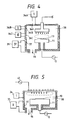
- FIG 4 is a schematic diagram showing another embodiment of the invention as applied to a parallel plate type plasma etching apparatus.
- the temperature controller 34 is divided into three parts 34A, 34B, 34C; the corresponding plasma generation regions in the vacuum container 38 are heated to respective desired temperatures; and the side surface and lower part of the specimen mount, the inner bottom portion of the processing chamber and the exhaust pipe are cooled to a desired temperature by the temperature controller 35.
- FIG. 5 shows another embodiment of this invention as applied to an induction coupled discharge type apparatus, one of the external energy supply discharge types.
- the temperature controller 34 is provided to the plasma generation region in the vacuum container 38 to heat the inner sidewall of the.processing chamber to a desired temperature, and the temperature controller 35 cools the side surface and lower part of the specimen mount, the inner bottom portion of the processing chamber and the exhaust pipe to a desired temperature.
- This construction produces the similar effect to that of the embodiment of Figure 1.
- FIG. 6 shows still another embodiment of this invention as applied to a parallel plate type plasma etching apparatus.
- the construction of the apparatus of Figure 6 is similar to the apparatus of Figure 4 except for the electrodes used for internal energy supply discharge. That is, in the apparatus of Figure 6, the temperature controller 34 is divided into three parts 34A, 34B, 34C to heat the plasma generation region in the vacuum container 38 to a desired temperature, while at the same time the side surface and lower part of the specimen mount, the inner bottom portion of the processing chamber and the exhaust pipe are cooled to a desired temperature by the temperature controller 35. This produces the similar effect to that of the embodiment of Figure 1.
- Figure 7 shows a further embodiment of this invention as applied to a type apparatus, one of the external energy supply discharge types.
- coil 34 is wound around a dome type discharge tube 14, the coil 34 is coupled to RF (radio frequency) power 40, a plasma is induced by the coil 34 which RF voltage is applied to, and the plasma is generated in a plasma generation region 38, the generated plasma heats the inner sidewall of the processing chamber to a desired temperature without providing temperature controller 34 such as other same time the side surface and lower part of the specimen mount, the inner bottom portion of the processing chamber and the exhaust pipe is cooled to a desired temperature by the temperature controller 35.
- This construction produces the similar effect to that of the embodiment of Figure 1.
- One of the ways to cope with this problem may provide the side surface and lower part of the specimen mount, the inner bottom portion of the processing chamber and the exhaust pipe with a plate-like component that has a temperature control function and a function of controlling the potential to a negative and a positive one.
- the temperature controller I of Figs. 1 and 5 and the temperature controllers I, II and III of Figs. 4 and 6 suitably comprise electrical resistance heaters extending around the plasma chamber.
- the temperature controller II of Figs. 1 and 5, the temperature controller IV of Figs. 4 and 6 and the temperature controller I of Fig. 7 may employ as coolant liquid nitrogen as mentioned, or another suitable coolant fluid which is heated or cooled to maintain it at a desired temperature.
- this invention it is possible to provide a plasma processing apparatus and method, which prevents reaction products from adhering to portions in the processing chamber (inner sidewall of the processing chamber and upper electrode) located higher than where an object to be processed is mounted, and which causes the reaction products to adhere only to those portions that are controlled at a temperature where the reaction products solidify, thereby minimizing the generation of foreign matters and improving the yield.
Abstract
Description
- The present invention relates to a plasma processing method and apparatus and more specifically to a plasma processing method and apparatus suited for plasma-processing specimens such as semiconductor device substrates.
- There has been available a technique of plasma-processing specimens of semiconductor devicesubstrates, as represented by a technique described in Japanese Patent Laid-Open No. 167825/1991. This publication limits the temperature control of a processing chamber where plasma is generated only to asidewall portion and deals with only reaction products that are generated after etching.
- The above-mentioned prior art is effective only for the reaction products adhering to the inner surface of the sidewall of the processing chamber and does not consider reaction products or gaseous reaction products adhering to electrodes, i.e., the lower part of the specimen mount, the inner bottom portion of the processing chamber and the exhaust pipe during the plasma processing.
- That is, reaction products also adhere to the lower part of the specimen mount, the inner bottom portion of the processing chamber and the exhaust pipe. During the plasma processing, these reaction products are not only deposited on these portions but also flake off contaminating the specimens, greatly reducing the yield of specimens.
- The object of this invention is to solve such problems. The invention provides a plasma processing method and apparatus, which controls the temperature of locations where reaction products or gaseous reaction products (hereinafter referred to as reaction products) adhere thereby preventing abnormal generation of reaction products and ensuring high yield of specimens.
- To achieve this, the locations above the specimen are controlled at temperatures at which the reaction products do not solidify and the locations below the specimen (lower part of the specimen mount, inner bottom portion of the processing chamber, exhaust pipe, etc.) are controlled at temperatures at which the reaction products solidify.
- With this invention, the portions, above the specimen, of the inner side surface of the processing chamber where plasma is generated (plasma generation portion) are set at temperatures at which reaction products sublimate, while the lower part of the specimen mount, the inner bottom portion of the processing chamber and the exhaust pipe are set at temperatures at which the reaction products solidify. This prevents the reaction products from adhering to locations above the specimen and therefore foreign matters from falling onto the surface of the specimen being processed. Reaction products and foreign matters floating in the processing chamber (hereinafter called floating foreign matters) adhere to or are trapped by the lower portion of the specimen mount, the inner bottom portion in the processing chamber and the exhaust pipe. While the vacuum is maintained, foreign matters can be prevented from being flaked off and the flaked matters from floating around because these locations are controlled at all times at temperatures at which reaction products solidify.
- Figure 1 is a vertical cross section showing a microwave plasma processing apparatus as one embodiment of this invention.
- Figure 2 is a vapor pressure curve diagram for etching gases and reaction products as one embodiment of this invention.
- Figure 3 is a control sequence diagram for the plasma processing apparatus as one embodiment of this invention.
- Figure 4 is a vertical cross section showing a parallel plate type plasma etching apparatus as another embodiment of this invention.
- Figure 5 is a vertical cross section showing an induction coupled discharge type apparatus as still another embodiment of this invention.
- Figure 6 is a vertical cross section showing a parallel plate type plasma etching apparatus as a further embodiment of this invention.
- Figure 7 is a vertical cross section showing a microwave discharge type apparatus as a further embodiment of this invention.
- Now, one embodiment of this invention will be described by referring to the accompanying drawings.
- Figure 1 is a vertical cross section of an essential portion of the microwave plasma processing apparatus showing its outline configuration as one embodiment of this invention.
- In Figure 1, a
processing chamber 10 has aquartz discharge tube 14 as its upper constitutional element.
Theprocessing chamber 10 is provided with agas supply port 15 connected to a gas source (not shown) for supplying an etching gas to theprocessing chamber 10, and also with anexhaust port 16 leading to a vacuum discharge apparatus (not shown). In theprocessing chamber 10 is installed aspecimen mount 11 on which to place a semiconductor device substrate (wafer) 13. Thespecimen mount 11 is connected to a highfrequency power source 12 so that a high frequency power can be applied to thespecimen mount 11. Thedischarge tube 14 is enclosed by awaveguide 17, on the outer side of which there is provided asolenoid coil 19 that produces a magnetic field in thedischarge tube 14. Thedischarge tube 14 in theprocessing chamber 10 is provided with a temperature controller I 34. Thewaveguide 17 is provided at its end with amagnetron 18 that oscillates microwaves. A lower part of the specimen mount, the inner bottom portion of the chamber and the exhaust pipe in theprocessing chamber 10 are also provided with a temperature controller II 35. - The temperature controllers I34, II35, control the temperature of the inner sidewall of the processing chamber at a desired temperature according to
temperature sensors - In the plasma processing apparatus of this construction, a processing gas for etching is supplied from the
gas supply port 15 into theprocessing chamber 10 and at the same time theprocessing chamber 10 is evacuated to a specified pressure. Then, microwaves are introduced into thedischarge tube 14 from themagnetron 18 through thewaveguide 17, and thesolenoid coil 19 generates a magnetic field to plasmatize the processing gas in thedischarge tube 14 by the interaction between the electric field of the microwaves and the magnetic field of thesolenoid coil 19. The highfrequency power source 12 applies a high frequency power to thespecimen mount 11 to produce a bias voltage and thereby draw ions in the plasma toward thewafer 13 to perform anisotropic etching on thewafer 13. At this time, the reaction products produced by etching are discharged from the sidewall and lower part of the specimen mount and from the inner bottom of the processing chamber through the exhaust pipe. - Next, the temperature control regions for the temperature controllers I34, II35 , are shown in Table 1. As shown in Table 1, the inner sidewall portion corresponding to the plasma generation region in the
processing chamber 10 is controlled at an elevated temperature range of 100°C and more than 100°C to 400°C and other portions, such as side surface and lower part of the specimen mount, the inner bottom portion of the processing chamber and the exhaust pipe, are cooled at -200°C or more than -200°C to less than 100°C. The reason why cooling temperature is set at more than -200°C or -200°C is based on the tool to cool the lower part of the chamber.
Liquid nitrogen is practically available and it can cool at about -200°C, so the cooling lowest limit is decided.Table 1 No. Heating Cooling I 100°C to 400°C - II - -200°C to 100°C - The temperature control is explained by referring to Figure 2. Figure 2 shows an example vapor pressure curve for the etching gas and reaction products in the case of aluminum wiring material.
- In Figure 2, when the aluminum wire is processed with gases BCl3 and Cl2, the reaction products are AlCl3 and are evaporated and discharged.
- The reaction product AlCl3 solidifies at 100 °C when the etching pressure is 1 Torr. That is, it is seen that reaction products are deposited when the inner sidewall of the processing chamber of the plasma processing apparatus of Figure 1 is lower than 100°C.
- Hence, if the plasma processing is performed continuously under this condition, deposits flake off as foreign matters in the processing chamber. With this embodiment, however, by setting the inner sidewall of the processing chamber at 100°C or more than 100°C and the lower part of the specimen mount, the inner bottom portion of the processing chamber and the exhaust pipe at lower than 100°C, it is possible to prevent the reaction products from adhering to the inner sidewall of the processing chamber and cause the reaction products to selectively adhere to the lower part of the specimen mount, the inner bottom of the processing chamber and the exhaust pipe, thereby minimizing foreign matters falling onto the surface of the wafer being etched or those floating from the inner bottom of the processing chamber.
- For other wiring materials, the similar effect is also obtained by putting under appropriate temperature conditions the processing chamber, the sidewall and lower part of the specimen mount, the inner bottom portion of the processing chamber and the exhaust pipe.
- Figure 3 shows the control sequence for the plasma processing apparatus of Figure 1.
- In Figure 3, before a wafer is introduced in the apparatus, the temperature controller I 34 controls the temperature of the inner sidewall of the processing chamber and the temperature controller II 35 controls the temperature of the side surface and lower part of the specimen mount, the inner bottom portion of the processing chamber and the exhaust pipe. After the wafer is introduced, the normal etching sequence is performed. After plasma processing is finished, the temperature controllers I34, II 35 are turned off and the apparatus is opened to air for normal cleaning.
- When the
temperature controller I 34 is started, theprocessing chamber 10 is heated to a predetermined temperature where it is controlled to be maintained. When the temperature controller II 35 is started, the lower portion of thespecimen mount 11, the inner bottom portion of theprocessing chamber 10 and the exhaust pipe are cooled to the predetermined temperature where they are controlled to be maintained. - Next, the
wafer 13, in this case, one, is carried into theprocessing chamber 10 by a wafer carrying device not shown. Thewafer 13 is transferred from the wafer carrying device onto the surface of the specimen mount, with the surface of the wafer to be etched facing up. Thewafer 13 thus mounted on thespecimen mount 11 is held immovable. - After or before the above operation is completed, the
processing chamber 10 is evacuated. By activating the evacuation device, the gases in theprocessing chamber 10 are discharged through the exhaust pipe fitted with an exhaust valve and a variable resistance valve (not shown). The pressure in theprocessing chamber 10 being evacuated is reduced to a specified pressure by adjusting the variable resistance valve. - Next, the etching gas is supplied from the gas supply source through the
gas supply port 15 into theprocessing chamber 10. The amount of etching gas supplied to theprocessing chamber 10 is controlled at a predetermined value by a gas flow controller (not shown). - Then, a part of the etching gas supplied into the
processing chamber 10 is discharged out of theprocessing chamber 10 by the evacuation device to control the pressure in theprocessing chamber 10 at a specified etching processing pressure. - Next, the
magnetron 18 and thesolenoid coil 19 are operated to plasmatize the etching gas in theprocessing chamber 10. As a result, the etching surface of thewafer 13 held on thespecimen mount 11 is processed by the plasma. At the same time, the highfrequency power source 12 is operated to apply the high frequency power to thespecimen mount 11, thereby applying a bias to thewafer 13. With the bias applied, the etching surface of thewafer 13 is etched. - When the etch processing of the
wafer 13 is completed in this way, the supply of etching gas to theprocessing chamber 10 and the operation of the highfrequency power source 12,magnetron 18 andsolenoid coil 19 are stopped. In this condition, the processedwafer 13 is transferred from thespecimen mount 11 to the wafer carrying device, which takes it out of theprocessing chamber 10. Then, anew wafer 13 is placed into theprocessing chamber 10 by the wafer carrying device, and the above-mentioned processing is performed. The temperature controllers I34,II 35 continue their operation to keep the temperatures of various portions of the apparatus at the controlled temperatures. In some cases, the operation of the temperature controllers I34,II 35, may be stopped between the wafer processing. For example, the apparatus is stopped when the wafer processing is interrupted for an extended period of time because of failure or for some other reasons, or when the work for the day has been finished. The operation of the temperature controllers I 34, II 35 is also stopped when the interior of theprocessing chamber 10 is opened to air for cleaning.
Particularly by stopping the operation of thetemperature controller II 35, it is possible to prevent impurities such as water contained in air from adhering to the cooled portions when theprocessing chamber 10 is opened to air. In this way, the inconveniences experienced at time of evacuation of the processing chamber 10 (prolonged evacuation time and failure to reach a specified pressure) can be eliminated. - The control temperatures of various portions controlled by the temperature controllers I 34, II 35 depend on the film quality of the
wafer 13, i.e., wiring material and the kind of etching gas. - Information on the
wafer 13 to be etched, such as wiring material and the kind of etching gas compatible with the wiring material, is entered into the higher level controller (not shown) by an operator. The higher level controller then outputs control signalsto the temperature controllers I 34, II 35, which in turn control the temperatures of various portions. - Such a temperature control is performed by an operator entering the information on the
wafer 13 through a touch panel or by reading the wafer information by some means into the higher level controller or directly into the temperature controllers I 34, II 35. - In this way, the temperatures of various portions can be controlled reliably at specified temperatures, thereby improving the wafer yield stably and reliably.
- The maintenance of the portions cooled by the temperature controller II 35 (cooled portions) in particular in performed as follows.
- The reaction products are made to adhere to the cooled portions, forming deposits there. The maintenance is performed before or when the deposit thickness reaches a point that causes an increase in exhaust resistance or produces foreign matters by deposit flaking. At this time, the cooling of the cooled portions by the
temperature controller II 35 is stopped. The cooled portions are then heated to the sublimation temperature of the deposit. As a result of heating, the deposit adhering to the cooled portion is sublimated and discharged out of theprocessing chamber 10 by operating the evacuation device. When the sublimation is finished, the heating of the cooled portions is stopped and the temperature control by thetemperature controller II 35 is performed. The heating of the cooled portions may be realized by adding a heating device (not shown) or by constructing the temperature controller II 35 to have the cooling and heating functions and switching between the functions. - Where the cleaning is done by opening the
processing chamber 10 to air, the maintenance of the cooled portions is done before opening theprocessing chamber 10 to air. Where the cleaning is done by plasma without opening theprocessing chamber 10 to air, the maintenance is performed before or during cleaning. When the maintenance is performed during cleaning and when the adhering deposit can be removed from the cooled portions, there is no need to heat the cooled portions. - This embodiment offers the following advantages.
- With the technique of heating the inner sidewall portion of the processing chamber, it is possible to prevent adhesion and deposition of reaction products produced by etching to the inner sidewall portion as mentioned above. Further, when this technique is employed to heat the lower part of the specimen mount, the inner bottom portion of the processing chamber and the exhaust pipe, the adhesion and deposition of reaction products to these portions can also be prevented.
- This technique, however, cannot remove foreign matters floating in the processing chamber and it is not possible to prevent reduction in wafer yield caused by floating foreign matters. This drawback becomes salient as the capacity of semiconductors increases to 65M and 256M. Further, because a major part of the reaction products is evacuated out of the processing chamber, the evacuation system including vacuum evacuation device, evacuation valve and variable resistance valve may be damaged. This problem becomes more serious when the reaction products are corrosive.
- As an alternative, a technique may be adopted which cools the lower part of the specimen mount, the inner bottom portion of the processing chamber and the exhaust pipe to cause the reaction products to adhere to the cooled portions.
- With this technique, however, because the coolingof the inner bottom portion of the processing chamber educes the temperature of the inner sidewall portion of the processing chamber below the evaporation point of reaction products, the reaction products and floating foreign matters adhere to or become deposited on the inner sidewall portion of the processing chamber. Because the inner sidewall portion of the processing chamber is located higher than the etching surface of the water being processed, the adhesion and deposition of reaction products to the inner sidewall portion are very disadvantageous in terms of wafer yield. That is, the deposit may flake off the inner sidewall portion of the processing clamber and fall as foreign matters onto the wafer being processed, lowering the yield.
- To deal with these problems, the embodiment of this invention heats the inner sidewall portion of the processing chamber to a temperature at which reaction products will not adhere to it and, at the same time, cools the lower part of the specimen mount, the inner bottom portion of the processing chamber and the exhaust pipe to a temperature at which the reaction products easily adhere to them.
This prevents foreign matters from being formed, thus improving the wafer yield. - In other words, this embodiment is characterized by the concept that the adhesion of reaction products to the inner sidewall portion of the processing chamber located higher than the etching surface of the wafer being processed is minimized while at the same time the reaction products and floating foreign matters are positively induced to adhere to the lower part of the specimen mount, the inner bottom portion of the processing chamber and the exhaust pipe, all located below the etching surface of the wafer. This concept is very effective for prevention of generation of foreign matters and for improvement of wafer yield.
- Further, because the reaction products are positively induced to adhere to particular locations, such as the lower part of the specimen mount, the inner bottom portion of the processing chamber and the exhaust pipe, it is possible to remove deposits adhering to these portions periodically and easily by cleaning, replacement and baking, improving the maintainability of the processing apparatus.
- Furthermore, because the reaction products and floating foreign matters are arrested to the extent that the evacuation system is not adversely affected, the conventional problem of the evacuation system being damaged by the reaction products and floating foreign matters is eliminated.
- This invention can also be applied to the constructions shown in Figure 4 to 7 in addition to the above embodiment.
- Figure 4 is a schematic diagram showing another embodiment of the invention as applied to a parallel plate type plasma etching apparatus. In the apparatus of Figure 4, the
temperature controller 34 is divided into threeparts vacuum container 38 are heated to respective desired temperatures; and the side surface and lower part of the specimen mount, the inner bottom portion of the processing chamber and the exhaust pipe are cooled to a desired temperature by thetemperature controller 35. This prevents the reaction products from adhering to the inner sidewall of the processing chamber and instead causes them to adhere selectively to the lower part of the specimen mount, the inner bottom portion of the processing chamber and the exhaust pipe, as in the embodiment of Figure 1. This in turn minimizes the chance of foreign matters falling onto the wafer or of foreign matters getting floated from the bottom of the processing chamber. - Figure 5 shows another embodiment of this invention as applied to an induction coupled discharge type apparatus, one of the external energy supply discharge types. In the apparatus of Figure 5, the
temperature controller 34 is provided to the plasma generation region in thevacuum container 38 to heat the inner sidewall of the.processing chamber to a desired temperature, and thetemperature controller 35 cools the side surface and lower part of the specimen mount, the inner bottom portion of the processing chamber and the exhaust pipe to a desired temperature.
This construction produces the similar effect to that of the embodiment of Figure 1. - Figure 6 shows still another embodiment of this invention as applied to a parallel plate type plasma etching apparatus. The construction of the apparatus of Figure 6 is similar to the apparatus of Figure 4 except for the electrodes used for internal energy supply discharge. That is, in the apparatus of Figure 6, the
temperature controller 34 is divided into threeparts vacuum container 38 to a desired temperature, while at the same time the side surface and lower part of the specimen mount, the inner bottom portion of the processing chamber and the exhaust pipe are cooled to a desired temperature by thetemperature controller 35. This produces the similar effect to that of the embodiment of Figure 1. - Figure 7 shows a further embodiment of this invention as applied to a type apparatus, one of the external energy supply discharge types. In the apparatus of Figure 7,
coil 34 is wound around a dometype discharge tube 14, thecoil 34 is coupled to RF (radio frequency)power 40, a plasma is induced by thecoil 34 which RF voltage is applied to, and the plasma is generated in aplasma generation region 38, the generated plasma heats the inner sidewall of the processing chamber to a desired temperature without providingtemperature controller 34 such as other same time the side surface and lower part of the specimen mount, the inner bottom portion of the processing chamber and the exhaust pipe is cooled to a desired temperature by thetemperature controller 35. This construction produces the similar effect to that of the embodiment of Figure 1. - Although the above embodiments do not mention the charges of foreign matters, the floating dust is very likely to be charged. One of the ways to cope with this problem may provide the side surface and lower part of the specimen mount, the inner bottom portion of the processing chamber and the exhaust pipe with a plate-like component that has a temperature control function and a function of controlling the potential to a negative and a positive one.
- The temperature controller I of Figs. 1 and 5 and the temperature controllers I, II and III of Figs. 4 and 6 suitably comprise electrical resistance heaters extending around the plasma chamber. The temperature controller II of Figs. 1 and 5, the temperature controller IV of Figs. 4 and 6 and the temperature controller I of Fig. 7 may employ as coolant liquid nitrogen as mentioned, or another suitable coolant fluid which is heated or cooled to maintain it at a desired temperature.
- With this invention, it is possible to provide a plasma processing apparatus and method, which prevents reaction products from adhering to portions in the processing chamber (inner sidewall of the processing chamber and upper electrode) located higher than where an object to be processed is mounted, and which causes the reaction products to adhere only to those portions that are controlled at a temperature where the reaction products solidify, thereby minimizing the generation of foreign matters and improving the yield.
Claims (9)
- A plasma processing method wherein a specimen is processed in a plasma processing apparatus which includes a plasma generation chamber to which a processing gas is supplied and whose pressure is maintained at a predetermined pressure, a specimen mount on which to mount the specimen to be processed in the plasma generation chamber, and an evacuation means to evacuate the plasma generation chamber;
the method comprising individually controlling the temperature of those portions in the plasma generation chamber where plasma is generated and the temperature of other portions to minimize variations with time in the characteristics of plasma-processing the specimen. - A plasma processing method wherein a specimen is processed in a plasma processing apparatus which includes a plasma generation chamber to which a processing gas is supplied to process a specimen and whose pressure is maintained at a predetermined pressure, a specimen mount on which to mount the specimen to be processed in the plasma generation chamber, and an evacuation means to evacuate the plasma generation chamber;
the method comprising the steps of:
maintaining a higher temperature of the sidewall of those portions in the plasma generation chamber where plasma is generated and cooling the inner wall of other portions. - A plasma processing method wherein a specimen is processed in a plasma processing apparatus which includes a plasma generation chamber to which a processing gas is supplied to process a specimen and whose pressure is maintained at a predetermined pressure, a specimen mount on which to mount the specimen to be processed in the plasma generation chamber, and an evacuation means to evacuate the plasma generation chamber;
the method comprising during the plasma processing maintaining internal surfaces of the chamber above the level of the specimen at a temperature such that reaction product does not form a deposit there, while cooling at least another part of the internal surface of the chamber to maintain a temperature lower than the solidification temperature of reaction product. - A plasma processing method according to any one of claims 1 to 3, wherein the temperature control on individual portions includes controlling the temperature of a passage of the processing gas and controlling the potential to negative or positive.
- A plasma processing apparatus comprising:a plasma generation chamber to which a processing gas is supplied to process a specimen;a specimen mount on which to mount an object to be processed in the plasma generation chamber;an evacuation means to evacuate the plasma generation chamber; anda temperature control means to control separately the temperature of those portions in the plasma generation chamber where plasma is generated and the temperature of other portions.
- A plasma processing apparatus according to claim 5 wherein the temperature control function controls the temperature of those portions where plasma is generated and the temperature of other portions by linking them to one of the temperatures.
- A plasma processing apparatus according to claim 5 or 6 wherein the temperature control function increases the temperature of the sidewall of the plasma generation chamber where plasma is generated and cools and inner wall of the chamber other than this sidewall.
- A plasma processing apparatus according to claim 5, 6 or 7 wherein the temperature control function can remove sidewall portions other than the sidewall of those portions where plasma is generated.
- A plasma processing apparatus comprising:a plasma generation chamber to which a processing gas is supplied to process a specimen;a specimen mount on which to mount an object to be processed in the plasma generation chamber;an evacuation means to evacuate the plasma generation chamber;characterized by cooling means for maintaining at least part of the internal surface of the chamber below the level of the specimen on the specimen mount at a temperature lower than that of the internal surface above the specimen level.
Applications Claiming Priority (2)
| Application Number | Priority Date | Filing Date | Title |
|---|---|---|---|
| JP6038395 | 1995-03-20 | ||
| JP60383/95 | 1995-03-20 |
Publications (2)
| Publication Number | Publication Date |
|---|---|
| EP0734047A2 true EP0734047A2 (en) | 1996-09-25 |
| EP0734047A3 EP0734047A3 (en) | 1997-04-02 |
Family
ID=13140580
Family Applications (1)
| Application Number | Title | Priority Date | Filing Date |
|---|---|---|---|
| EP96301870A Withdrawn EP0734047A3 (en) | 1995-03-20 | 1996-03-19 | Plasma processing method and apparatus |
Country Status (5)
| Country | Link |
|---|---|
| US (1) | US5961850A (en) |
| EP (1) | EP0734047A3 (en) |
| KR (1) | KR100399542B1 (en) |
| SG (1) | SG47090A1 (en) |
| TW (1) | TW297135B (en) |
Cited By (2)
| Publication number | Priority date | Publication date | Assignee | Title |
|---|---|---|---|---|
| EP1139398A1 (en) * | 1998-10-14 | 2001-10-04 | Tokyo Electron Limited | Method and apparatus for surface treatment |
| US6815365B2 (en) | 1995-03-16 | 2004-11-09 | Hitachi, Ltd. | Plasma etching apparatus and plasma etching method |
Families Citing this family (30)
| Publication number | Priority date | Publication date | Assignee | Title |
|---|---|---|---|---|
| US6092486A (en) * | 1996-05-27 | 2000-07-25 | Sumimoto Metal Indsutries, Ltd. | Plasma processing apparatus and plasma processing method |
| US6176929B1 (en) * | 1997-07-22 | 2001-01-23 | Ebara Corporation | Thin-film deposition apparatus |
| US6129807A (en) * | 1997-10-06 | 2000-10-10 | Applied Materials, Inc. | Apparatus for monitoring processing of a substrate |
| US6201219B1 (en) * | 1998-02-25 | 2001-03-13 | Micron Technology, Inc. | Chamber and cleaning process therefor |
| JP3764594B2 (en) * | 1998-10-12 | 2006-04-12 | 株式会社日立製作所 | Plasma processing method |
| US6221203B1 (en) * | 1999-06-01 | 2001-04-24 | Taiwan Semiconductor Manufacturing Co., Ltd | Apparatus and method for controlling temperature of a chamber |
| US6547922B2 (en) * | 2000-01-31 | 2003-04-15 | Canon Kabushiki Kaisha | Vacuum-processing apparatus using a movable cooling plate during processing |
| US6666924B1 (en) * | 2000-03-28 | 2003-12-23 | Asm America | Reaction chamber with decreased wall deposition |
| US20050106868A1 (en) * | 2002-01-01 | 2005-05-19 | Asao Yamashita | Etching method |
| JP4043488B2 (en) * | 2003-02-04 | 2008-02-06 | 東京エレクトロン株式会社 | Processing system and method of operating the processing system |
| JP4058364B2 (en) * | 2003-03-18 | 2008-03-05 | 株式会社日立製作所 | Semiconductor manufacturing equipment |
| US20060000551A1 (en) * | 2004-06-30 | 2006-01-05 | Saldana Miguel A | Methods and apparatus for optimal temperature control in a plasma processing system |
| US8540843B2 (en) | 2004-06-30 | 2013-09-24 | Lam Research Corporation | Plasma chamber top piece assembly |
| US7780791B2 (en) * | 2004-06-30 | 2010-08-24 | Lam Research Corporation | Apparatus for an optimized plasma chamber top piece |
| JP4997842B2 (en) * | 2005-10-18 | 2012-08-08 | 東京エレクトロン株式会社 | Processing equipment |
| KR100698927B1 (en) * | 2005-12-13 | 2007-03-23 | 주식회사 래디언테크 | Plasma processing method |
| US20070281106A1 (en) * | 2006-05-30 | 2007-12-06 | Applied Materials, Inc. | Process chamber for dielectric gapfill |
| WO2008030047A1 (en) * | 2006-09-06 | 2008-03-13 | Seoul National University Industry Foundation | Apparatus and method of depositing films using bias and charging behavior of nanoparticles formed during chemical vapor deposition |
| GB2462589B (en) * | 2008-08-04 | 2013-02-20 | Sony Comp Entertainment Europe | Apparatus and method of viewing electronic documents |
| US9285168B2 (en) | 2010-10-05 | 2016-03-15 | Applied Materials, Inc. | Module for ozone cure and post-cure moisture treatment |
| US8664127B2 (en) | 2010-10-15 | 2014-03-04 | Applied Materials, Inc. | Two silicon-containing precursors for gapfill enhancing dielectric liner |
| US10283321B2 (en) | 2011-01-18 | 2019-05-07 | Applied Materials, Inc. | Semiconductor processing system and methods using capacitively coupled plasma |
| US20120180954A1 (en) | 2011-01-18 | 2012-07-19 | Applied Materials, Inc. | Semiconductor processing system and methods using capacitively coupled plasma |
| US8716154B2 (en) | 2011-03-04 | 2014-05-06 | Applied Materials, Inc. | Reduced pattern loading using silicon oxide multi-layers |
| US9404178B2 (en) | 2011-07-15 | 2016-08-02 | Applied Materials, Inc. | Surface treatment and deposition for reduced outgassing |
| CN103165368B (en) * | 2011-12-16 | 2016-02-03 | 中微半导体设备(上海)有限公司 | The plasm restraint device that a kind of temperature is adjustable |
| US8889566B2 (en) | 2012-09-11 | 2014-11-18 | Applied Materials, Inc. | Low cost flowable dielectric films |
| US9018108B2 (en) | 2013-01-25 | 2015-04-28 | Applied Materials, Inc. | Low shrinkage dielectric films |
| US9412581B2 (en) | 2014-07-16 | 2016-08-09 | Applied Materials, Inc. | Low-K dielectric gapfill by flowable deposition |
| KR102323320B1 (en) * | 2015-05-13 | 2021-11-09 | 세메스 주식회사 | Apparatus and method for treating substrate comprising the same |
Citations (4)
| Publication number | Priority date | Publication date | Assignee | Title |
|---|---|---|---|---|
| DE3140237A1 (en) * | 1980-10-09 | 1982-06-09 | Mitsubishi Denki K.K., Tokyo | PLASMA EQUIPMENT |
| JPH03167825A (en) * | 1989-11-28 | 1991-07-19 | Matsushita Electric Ind Co Ltd | Etching device and etching method |
| JPH06188220A (en) * | 1992-12-18 | 1994-07-08 | Hitachi Ltd | Microwave plasma treatment and device therefor |
| EP0650182A1 (en) * | 1993-10-15 | 1995-04-26 | Applied Materials, Inc. | Plasma etch reactors and methods of operating thereof |
Family Cites Families (7)
| Publication number | Priority date | Publication date | Assignee | Title |
|---|---|---|---|---|
| US5102496A (en) * | 1989-09-26 | 1992-04-07 | Applied Materials, Inc. | Particulate contamination prevention using low power plasma |
| JP2532401Y2 (en) * | 1991-04-16 | 1997-04-16 | ソニー株式会社 | Bias ECR plasma CVD equipment |
| US5368685A (en) * | 1992-03-24 | 1994-11-29 | Hitachi, Ltd. | Dry etching apparatus and method |
| JP3227522B2 (en) * | 1992-10-20 | 2001-11-12 | 株式会社日立製作所 | Microwave plasma processing method and apparatus |
| KR0141659B1 (en) * | 1993-07-19 | 1998-07-15 | 가나이 쓰토무 | An apparatus for removing foreign particles and the method |
| US5647945A (en) * | 1993-08-25 | 1997-07-15 | Tokyo Electron Limited | Vacuum processing apparatus |
| US5616208A (en) * | 1993-09-17 | 1997-04-01 | Tokyo Electron Limited | Vacuum processing apparatus, vacuum processing method, and method for cleaning the vacuum processing apparatus |
-
1996
- 1996-03-12 TW TW085102995A patent/TW297135B/zh not_active IP Right Cessation
- 1996-03-14 US US08/615,949 patent/US5961850A/en not_active Expired - Lifetime
- 1996-03-19 EP EP96301870A patent/EP0734047A3/en not_active Withdrawn
- 1996-03-19 KR KR1019960007294A patent/KR100399542B1/en not_active IP Right Cessation
- 1996-03-20 SG SG1996006453A patent/SG47090A1/en unknown
Patent Citations (4)
| Publication number | Priority date | Publication date | Assignee | Title |
|---|---|---|---|---|
| DE3140237A1 (en) * | 1980-10-09 | 1982-06-09 | Mitsubishi Denki K.K., Tokyo | PLASMA EQUIPMENT |
| JPH03167825A (en) * | 1989-11-28 | 1991-07-19 | Matsushita Electric Ind Co Ltd | Etching device and etching method |
| JPH06188220A (en) * | 1992-12-18 | 1994-07-08 | Hitachi Ltd | Microwave plasma treatment and device therefor |
| EP0650182A1 (en) * | 1993-10-15 | 1995-04-26 | Applied Materials, Inc. | Plasma etch reactors and methods of operating thereof |
Non-Patent Citations (2)
| Title |
|---|
| PATENT ABSTRACTS OF JAPAN vol. 015, no. 408 (E-1123), 17 October 1991 & JP 03 167825 A (MATSUSHITA ELECTRIC IND CO LTD), 19 July 1991, * |
| PATENT ABSTRACTS OF JAPAN vol. 018, no. 527 (E-1613), 5 October 1994 & JP 06 188220 A (HITACHI LTD), 8 July 1994, * |
Cited By (4)
| Publication number | Priority date | Publication date | Assignee | Title |
|---|---|---|---|---|
| US6815365B2 (en) | 1995-03-16 | 2004-11-09 | Hitachi, Ltd. | Plasma etching apparatus and plasma etching method |
| US7208422B2 (en) | 1995-03-16 | 2007-04-24 | Hitachi, Ltd. | Plasma processing method |
| US7565879B2 (en) | 1995-03-16 | 2009-07-28 | Hitachi, Ltd | Plasma processing apparatus |
| EP1139398A1 (en) * | 1998-10-14 | 2001-10-04 | Tokyo Electron Limited | Method and apparatus for surface treatment |
Also Published As
| Publication number | Publication date |
|---|---|
| SG47090A1 (en) | 1998-03-20 |
| TW297135B (en) | 1997-02-01 |
| KR100399542B1 (en) | 2004-01-07 |
| EP0734047A3 (en) | 1997-04-02 |
| KR960035872A (en) | 1996-10-28 |
| US5961850A (en) | 1999-10-05 |
Similar Documents
| Publication | Publication Date | Title |
|---|---|---|
| EP0734047A2 (en) | Plasma processing method and apparatus | |
| US5935373A (en) | Plasma processing apparatus | |
| US6214162B1 (en) | Plasma processing apparatus | |
| US5585012A (en) | Self-cleaning polymer-free top electrode for parallel electrode etch operation | |
| US6171438B1 (en) | Plasma processing apparatus and plasma processing method | |
| US5707498A (en) | Avoiding contamination from induction coil in ionized sputtering | |
| KR100345420B1 (en) | Plasma Treatment Equipment | |
| JP3210207B2 (en) | Plasma processing equipment | |
| EP0653775B1 (en) | Microwave plasma processing apparatus and method | |
| KR20010030159A (en) | Plasma processing apparatus | |
| JPH1041378A (en) | Wafer support having pressure zone where temperature feedback and contact area are small | |
| KR102396430B1 (en) | Substrate processing apparatus and substrate processing method | |
| JPWO2002065532A1 (en) | Method for treating object to be treated and apparatus for treating the same | |
| KR19980071126A (en) | Applied vacuum chamber to reduce pump down time and base pressure | |
| JP2879887B2 (en) | Plasma processing method | |
| US20050236109A1 (en) | Plasma etching apparatus and plasma etching method | |
| US6547934B2 (en) | Reduction of metal oxide in a dual frequency etch chamber | |
| JPH07312348A (en) | Method and apparatus for treatment | |
| US5897740A (en) | Plasma processing system | |
| JP4473410B2 (en) | Sputtering apparatus and film forming method | |
| JP2869384B2 (en) | Plasma processing method | |
| KR20120137426A (en) | Sputtering apparatus and sputtering method | |
| EP0462563B1 (en) | Treating apparatus for semiconductor | |
| US11898236B2 (en) | Methods and apparatus for processing a substrate | |
| KR19980070035A (en) | Sputtering apparatus for making barrier film for integrated circuit |
Legal Events
| Date | Code | Title | Description |
|---|---|---|---|
| PUAI | Public reference made under article 153(3) epc to a published international application that has entered the european phase |
Free format text: ORIGINAL CODE: 0009012 |
|
| AK | Designated contracting states |
Kind code of ref document: A2 Designated state(s): DE GB IT |
|
| PUAL | Search report despatched |
Free format text: ORIGINAL CODE: 0009013 |
|
| AK | Designated contracting states |
Kind code of ref document: A3 Designated state(s): DE GB IT |
|
| 17P | Request for examination filed |
Effective date: 19970930 |
|
| 17Q | First examination report despatched |
Effective date: 19990510 |
|
| STAA | Information on the status of an ep patent application or granted ep patent |
Free format text: STATUS: THE APPLICATION IS DEEMED TO BE WITHDRAWN |
|
| 18D | Application deemed to be withdrawn |
Effective date: 19990921 |