EP0739112A2 - Electronic devices and operating mode control thereof - Google Patents
Electronic devices and operating mode control thereof Download PDFInfo
- Publication number
- EP0739112A2 EP0739112A2 EP19960302754 EP96302754A EP0739112A2 EP 0739112 A2 EP0739112 A2 EP 0739112A2 EP 19960302754 EP19960302754 EP 19960302754 EP 96302754 A EP96302754 A EP 96302754A EP 0739112 A2 EP0739112 A2 EP 0739112A2
- Authority
- EP
- European Patent Office
- Prior art keywords
- bus
- bias voltage
- operating mode
- initialization process
- outputted
- Prior art date
- Legal status (The legal status is an assumption and is not a legal conclusion. Google has not performed a legal analysis and makes no representation as to the accuracy of the status listed.)
- Granted
Links
Images

Classifications
-
- H—ELECTRICITY
- H04—ELECTRIC COMMUNICATION TECHNIQUE
- H04L—TRANSMISSION OF DIGITAL INFORMATION, e.g. TELEGRAPHIC COMMUNICATION
- H04L12/00—Data switching networks
- H04L12/02—Details
- H04L12/12—Arrangements for remote connection or disconnection of substations or of equipment thereof
-
- H—ELECTRICITY
- H04—ELECTRIC COMMUNICATION TECHNIQUE
- H04L—TRANSMISSION OF DIGITAL INFORMATION, e.g. TELEGRAPHIC COMMUNICATION
- H04L12/00—Data switching networks
- H04L12/28—Data switching networks characterised by path configuration, e.g. LAN [Local Area Networks] or WAN [Wide Area Networks]
- H04L12/40—Bus networks
- H04L12/40006—Architecture of a communication node
- H04L12/40013—Details regarding a bus controller
-
- H—ELECTRICITY
- H04—ELECTRIC COMMUNICATION TECHNIQUE
- H04L—TRANSMISSION OF DIGITAL INFORMATION, e.g. TELEGRAPHIC COMMUNICATION
- H04L12/00—Data switching networks
- H04L12/28—Data switching networks characterised by path configuration, e.g. LAN [Local Area Networks] or WAN [Wide Area Networks]
- H04L12/40—Bus networks
- H04L12/40006—Architecture of a communication node
- H04L12/40039—Details regarding the setting of the power status of a node according to activity on the bus
-
- H—ELECTRICITY
- H04—ELECTRIC COMMUNICATION TECHNIQUE
- H04L—TRANSMISSION OF DIGITAL INFORMATION, e.g. TELEGRAPHIC COMMUNICATION
- H04L12/00—Data switching networks
- H04L12/28—Data switching networks characterised by path configuration, e.g. LAN [Local Area Networks] or WAN [Wide Area Networks]
- H04L12/40—Bus networks
- H04L12/40052—High-speed IEEE 1394 serial bus
- H04L12/40117—Interconnection of audio or video/imaging devices
-
- Y—GENERAL TAGGING OF NEW TECHNOLOGICAL DEVELOPMENTS; GENERAL TAGGING OF CROSS-SECTIONAL TECHNOLOGIES SPANNING OVER SEVERAL SECTIONS OF THE IPC; TECHNICAL SUBJECTS COVERED BY FORMER USPC CROSS-REFERENCE ART COLLECTIONS [XRACs] AND DIGESTS
- Y02—TECHNOLOGIES OR APPLICATIONS FOR MITIGATION OR ADAPTATION AGAINST CLIMATE CHANGE
- Y02D—CLIMATE CHANGE MITIGATION TECHNOLOGIES IN INFORMATION AND COMMUNICATION TECHNOLOGIES [ICT], I.E. INFORMATION AND COMMUNICATION TECHNOLOGIES AIMING AT THE REDUCTION OF THEIR OWN ENERGY USE
- Y02D30/00—Reducing energy consumption in communication networks
- Y02D30/50—Reducing energy consumption in communication networks in wire-line communication networks, e.g. low power modes or reduced link rate
Definitions
- This invention relates to electronic devices and to operating mode control thereof.
- FIG. 1 An example of this kind of system is shown in FIG. 1.
- the electronic devices A to D are the aforementioned personal computers and digital video tape recorders etc.
- P1394 serial bus cables 111, 112 and 113 then make connections across the ports P of the electronic devices A and B, B and C and C and D.
- These electronic devices are referred to as nodes in the following specification.
- a pair of shielded twisted-pair cables (not shown in the drawings) are provided within these P1394 serial cables. Of this pair of twisted-pair cables, one pair is used for data transmission and the other pair is used for strobe signal transmission. Further, each node outputs a bias voltage for one twisted-pair cable and the bias voltage is detected on the other twisted-pair cable.
- each of the nodes is equipped with a physical layer controller (PHY) 114, a link layer controller (LINK) 115 and a central processing unit (hereinafter referred to as "CPU") 116 as a basic structure for carrying out communications on the P1394 serial bus.
- the physical layer controller 114 has functions for bus initialization, data encoding/decoding, arbitration and bias voltage output/detection etc.
- the link layer controller 115 has link layer controller functions for error correction code generation/detection and packet generation/detection etc.
- the CPU 116 has an application layer function.
- the physical layer controller 114 outputs a bias voltage onto the twisted-pair cable of the P1394 serial bus cable 111.
- This bias voltage is detected by the physical layer controller of node B connected directly by the P1394 serial bus cable 111.
- the node B knows that a node is connected by the P1394 serial bus cable 111.
- a bus reset occurs when a the bias voltage outputted to the bus by the physical layer controller of this node is detected by the physical layer controllers of the other nodes and physical address allocation for each node by the physical layer controllers of each node is automatically completed within at least 170 ⁇ sec.
- the nodes B to D commence transactions necessary at the time of bus reset decided by the' protocol. For example, a packet for interrogating as to what type of equipment etc. the node A is transmitted. The transaction is then completed by the node A correctly transmitting a packet in response to the interrogation.
- the CPU 116 has to carry out various internal initialization processes directly after the power supply is thrown.
- Other nodes cannot then receive response packets from node A because node A cannot respond to interrogations from other nodes during this time. The node A therefore experiences a time-out and the system may hang up.
- Isochronous hereinafter abbreviated to "Iso"
- a transaction is generated for carrying out confirmation of the communication channel and band for a uniquely designated resolver node when resetting the bus.
- the node A becomes the resolver node, other nodes cannot start ISO communication until the node A completes initialization.
- an electronic device is employed in a system where packets are sent and received between a plurality of electronic devices connected by a bus, in such a manner that a bias voltage is not outputted to the bus in a first operating mode operated in from when a power supply is thrown until an internal initialization process is complete and a bias voltage is outputted to the bus in a second operating mode operated in after the initialization process is complete.
- the initialization process can be an initialization of internal information necessary for transmitting and receiving packets.
- the electronic device can have a physical layer controller for outputting the bias voltage and the initialization process can be carried out by a central processing unit.
- an operating mode control method for an electronic device employed in a system for carrying out communication between a plurality of electronic devices connected by a bus comprises the steps of configuring the electronic device in such a manner that a bias voltage is not outputted to the bus in a first operating mode operated in from when a power supply is thrown until an internal initialization process is complete and outputting a bias voltage to the bus in a second operating mode operated in after the initialization process is complete.
- the initialization process can be an initialization of internal information necessary for transmitting and receiving packets.
- a bias voltage is not outputted to the bus from when the power supply is thrown until an internal initialization process is complete and a bias voltage is outputted to the bus after an internal initialization process is complete.
- a preferred form of implementation of the invention provides, for electronic devices connected to, for example, P1394 serial buses, operating mode control technology for preventing hang-ups during bus resets.
- the preferred form of implementation of the invention provides an electronic device and operating mode control method which do not cause the communications system to hang-up when the power supply is thrown.
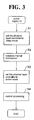
- FIG. 3 is a flowchart showing the operation of the CPU 3 shown in FIG. 2.
- step S1 When the power supply for the node goes on, the CPU 3 first sends out a control signal (step S1) for putting the physical layer controller 1 into sleep mode. In this way, the physical layer controller 1 goes into sleep mode and the operation of outputting a bias voltage to the bus is not carried out even if a power supply voltage is provided so that a bus reset does not occur. Further, on the other hand, even if the physical layer controller 1 outputs a bias voltage and a bus reset occurs sooner than the sending-out of a control signal for putting the physical layer controller 1 into sleep mode, a bus reset occurs again soon to put the physical layer controller 1 into sleep mode and the communications system goes into an un-connected state.
- step S2 and S3 the internal initialization process for the category table 4, the counter 5, the timer 6 and the buffer 7 is carried out and the physical layer controller 1 undergoes a transition (step S2 and S3) into active mode if a state where a transaction process can be carried out is attained.
- the internal initialization process consists of the following internal information initialization processes for starting transactions: initialization of a table for managing whether or not a response transaction has come for a sent request transaction; a timer initialization used in cases where a response transaction for a sent request transaction is waited for; initialization of a table used when it is necessary to re-send a sent request transaction or response transaction; and an initialization of a transmitted number counter used when it is necessary to re-send a sent request transaction or a response transaction.
- the CPU 3 controls other integrated circuits (not shown in the drawings) there are also other initialization processes i.e. a buffer initialization and an integrated circuit initialization for carrying out communications with the other integrated circuits.
- step S3 the physical layer controller 1 goes into active mode and this node outputs a bias voltage to the bus.
- this node and other nodes connected by the bus are aware that a new node has been connected to the communications system and a bus reset occurs.
- the aforementioned various transaction processes are then carried out between this node and other nodes.
- a state such as that for the related art where, for example ISO communications cannot be carried out does not occur because the initialization process for this node is already complete.
- the physical layer controller 1 is connected to a link layer controller 2 by the internal bus 11, with other nodes (not shown in the drawings) being connected by a P1394 serial bus 8.
- a driver and receiver 12 connected to the P1394 serial bus and an encoder and decoder 13 connected to the driver and receiver 12 are provided within the physical layer controller 1 as a circuit for transmitting and receiving signals to and from the P1394 serial bus 8.
- the driver and receiver 12 carries out transmitting and receiving of signals for the P1394 serial bus.
- the encoder and decoder 13 carries out transmission signal encoding and receive-signal decoding, as well as carrying out communications with the CPU 3 and link layer controller 2 via the internal bus 11.
- the driver and receiver 12 and the encoder and decoder 13 do not participate in the control of the operating modes of the physical layer controller 1.
- the CPU 3 sends an instruction signal for setting up the sleep mode at the physical layer controller 1 to the bias input/output controller 15 until the internal initialization process described with reference to FIG. 2 is complete.
- the bias input/output controller 15 then receives this instruction signal and instructs the bias output control circuit 17 not to output the bias voltage Vb generated by the constant voltage circuit 16 to the P1394 serial bus 8.
- the bias voltage Vb is not outputted to the twisted pair cable of the P1394 serial bus 8 because the bias voltage Vb generated by the constant voltage circuit 16 cannot pass through the bias output control circuit 17.
- the CPU 3 sends an instruction signal for setting up the active mode at the physical layer controller 1 to the bias input/output controller 15 when the internal initialization process is complete.
- the bias input/output controller 15 then receives this instruction signal and instructs the bias output control circuit 17 to output the bias voltage Vb generated by the constant voltage circuit 16 to the P1394 serial bus 8.
- the bias voltage Vb generated by the constant voltage circuit 16 passes through the bias output control circuit 17 and is outputted to the twisted pair cable of the P1394 serial bus 8.
- the bias voltage outputted to the P1394 serial bus 8 is detected by physical layer controllers of nodes connected to this bus 8 and a bus reset occurs as a result.
- sleep mode for the physical layer controller is when the power supply voltage Vcc is provided but the bias voltage is not outputted to the bus.
- sleep mode may also be when the power supply voltage Vcc is not provided, with the effect that the bias voltage is not outputted to the bus.
- an operation mode is set-up where a bias voltage is not outputted to the bus from when the power supply is thrown until the initialization process is complete and a bus reset therefore does not occur until the initialization process is complete. For example, even if an instantaneous bias voltage is outputted and' a bus reset occurs, the outputting of the bias voltage will be halted sufficiently quickly enough for the system to not hang up, the bus will be reset again and the communication system will be in a non-connected state. As a result, communication system hang-ups at the time of throwing the power supply can be avoided.
Abstract
Description
- This invention relates to electronic devices and to operating mode control thereof.
- Systems where electronic devices such as personal computers, digital tape recorders and digital television receivers are connected using a P1394 serial bus and packets for digital video signals, digital audio signals and control signals are sent and received between these electronic devices can be considered.
- An example of this kind of system is shown in FIG. 1. In FIG. 1, the electronic devices A to D are the aforementioned personal computers and digital video tape recorders etc. P1394
serial bus cables - A pair of shielded twisted-pair cables (not shown in the drawings) are provided within these P1394 serial cables. Of this pair of twisted-pair cables, one pair is used for data transmission and the other pair is used for strobe signal transmission. Further, each node outputs a bias voltage for one twisted-pair cable and the bias voltage is detected on the other twisted-pair cable.
- As shown in FIG. 1, each of the nodes is equipped with a physical layer controller (PHY) 114, a link layer controller (LINK) 115 and a central processing unit (hereinafter referred to as "CPU") 116 as a basic structure for carrying out communications on the P1394 serial bus. The
physical layer controller 114 has functions for bus initialization, data encoding/decoding, arbitration and bias voltage output/detection etc. Further, thelink layer controller 115 has link layer controller functions for error correction code generation/detection and packet generation/detection etc. TheCPU 116 has an application layer function. - With the communication system constructed in this way, when the power supply of node A goes from off to on with the nodes B to D on in a normal operating state, a power supply voltage is supplied to the
physical layer controller 114, thelink layer controller 115 and theCPU 116 of the node A and normal operation begins. - At this time, the
physical layer controller 114 outputs a bias voltage onto the twisted-pair cable of the P1394serial bus cable 111. This bias voltage is detected by the physical layer controller of node B connected directly by the P1394serial bus cable 111. As a result, the node B knows that a node is connected by the P1394serial bus cable 111. - In this way, a new node is connected to the bus, a bus reset occurs when a the bias voltage outputted to the bus by the physical layer controller of this node is detected by the physical layer controllers of the other nodes and physical address allocation for each node by the physical layer controllers of each node is automatically completed within at least 170 µsec. The details of this point are defined in the specification for the IEEE-P1394 serial bus and a detailed description is therefore omitted.
- When a bus reset occurs and physical address allocation for each of the nodes is complete, the nodes B to D commence transactions necessary at the time of bus reset decided by the' protocol. For example, a packet for interrogating as to what type of equipment etc. the node A is transmitted. The transaction is then completed by the node A correctly transmitting a packet in response to the interrogation.
- However, usually, the
CPU 116 has to carry out various internal initialization processes directly after the power supply is thrown. The time necessary changes depending on what kind of machine the node is and what process the node is carrying out, but is usually from a few tens of milliseconds to a few seconds. Other nodes cannot then receive response packets from node A because node A cannot respond to interrogations from other nodes during this time. The node A therefore experiences a time-out and the system may hang up. - For example, in order to carry out Isochronous (hereinafter abbreviated to "Iso") communications, a transaction is generated for carrying out confirmation of the communication channel and band for a uniquely designated resolver node when resetting the bus. However, if the node A becomes the resolver node, other nodes cannot start ISO communication until the node A completes initialization.
- According to the present invention, an electronic device is employed in a system where packets are sent and received between a plurality of electronic devices connected by a bus, in such a manner that a bias voltage is not outputted to the bus in a first operating mode operated in from when a power supply is thrown until an internal initialization process is complete and a bias voltage is outputted to the bus in a second operating mode operated in after the initialization process is complete.
- The initialization process can be an initialization of internal information necessary for transmitting and receiving packets. The electronic device can have a physical layer controller for outputting the bias voltage and the initialization process can be carried out by a central processing unit.
- Further, according to the present invention, an operating mode control method for an electronic device employed in a system for carrying out communication between a plurality of electronic devices connected by a bus, comprises the steps of configuring the electronic device in such a manner that a bias voltage is not outputted to the bus in a first operating mode operated in from when a power supply is thrown until an internal initialization process is complete and outputting a bias voltage to the bus in a second operating mode operated in after the initialization process is complete.
- The initialization process can be an initialization of internal information necessary for transmitting and receiving packets.
- According to the present invention, a bias voltage is not outputted to the bus from when the power supply is thrown until an internal initialization process is complete and a bias voltage is outputted to the bus after an internal initialization process is complete.
- A preferred form of implementation of the invention provides, for electronic devices connected to, for example, P1394 serial buses, operating mode control technology for preventing hang-ups during bus resets.
- The preferred form of implementation of the invention provides an electronic device and operating mode control method which do not cause the communications system to hang-up when the power supply is thrown.
- The invention will now be further described, by way of illustrative and non-limiting example, with reference to the accompanying drawings, in which:
- FIG. 1 is a view showing an example of a system for carrying out communications with a plurality of nodes connected by a P1394 serial bus;
- FIG. 2 is a block view showing the structure of parts of a node according to an embodiment of the present invention;
- FIG. 3 is a flowchart showing the operation of a
CPU 3 of FIG. 1; and - FIG. 4 is a block diagram showing an example of the structure of a physical layer controller of FIG. 2.
- The following is a detailed description with reference to the drawings of an embodiment of the present invention.
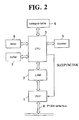
- FIG. 2 is a block diagram showing the main parts of the structure of a node according to an embodiment of the present invention. As shown in FIG. 2, the node of this embodiment is equipped with a
physical layer controller 1, alink layer controller 2 connected to thephysical layer controller 1 by the internal bus, aCPU 3 connected to thelink layer controller 2 by the internal bus, and a category table 4,counter 5,timer 6 andbuffer 7 also connected to theCPU 3 by the internal bus. A P1394 serial bus 8 is connected to the port (not shown in the diagrams) of thephysical layer controller 1. Further, theCPU 3 is constructed in such a manner as to control the operating modes of the physical layer controller 1 (described in detail later). - In this embodiment, the
physical layer controller 1 has two operating modes, a sleep mode (1) and an active mode (2). In sleep mode, the physical layer controller does not output a bias voltage to the bus even if a power supply voltage is provided and transmitting and receiving of packets is not carried out. Thephysical layer controller 1 carries out normal operation in active mode, i.e. a bias voltage is outputted to the bus and packets are transmitted and received. - Next, the operation is described at the time of throwing of the power supply for the node shown in FIG. 2. FIG. 3 is a flowchart showing the operation of the
CPU 3 shown in FIG. 2. - When the power supply for the node goes on, the
CPU 3 first sends out a control signal (step S1) for putting thephysical layer controller 1 into sleep mode. In this way, thephysical layer controller 1 goes into sleep mode and the operation of outputting a bias voltage to the bus is not carried out even if a power supply voltage is provided so that a bus reset does not occur. Further, on the other hand, even if thephysical layer controller 1 outputs a bias voltage and a bus reset occurs sooner than the sending-out of a control signal for putting thephysical layer controller 1 into sleep mode, a bus reset occurs again soon to put thephysical layer controller 1 into sleep mode and the communications system goes into an un-connected state. - Next, the internal initialization process for the category table 4, the
counter 5, thetimer 6 and thebuffer 7 is carried out and thephysical layer controller 1 undergoes a transition (step S2 and S3) into active mode if a state where a transaction process can be carried out is attained. - The internal initialization process consists of the following internal information initialization processes for starting transactions: initialization of a table for managing whether or not a response transaction has come for a sent request transaction; a timer initialization used in cases where a response transaction for a sent request transaction is waited for; initialization of a table used when it is necessary to re-send a sent request transaction or response transaction; and an initialization of a transmitted number counter used when it is necessary to re-send a sent request transaction or a response transaction. When the
CPU 3 controls other integrated circuits (not shown in the drawings) there are also other initialization processes i.e. a buffer initialization and an integrated circuit initialization for carrying out communications with the other integrated circuits. - In step S3, the
physical layer controller 1 goes into active mode and this node outputs a bias voltage to the bus. In this way, this node and other nodes connected by the bus are aware that a new node has been connected to the communications system and a bus reset occurs. The aforementioned various transaction processes (step S4) are then carried out between this node and other nodes. At this time, a state such as that for the related art where, for example ISO communications cannot be carried out does not occur because the initialization process for this node is already complete. - Next, an example of the circuit structure for a physical layer controller for executing the aforementioned operation is described with reference to FIG. 4.
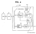
- As shown in FIG. 4, the
physical layer controller 1 is connected to alink layer controller 2 by the internal bus 11, with other nodes (not shown in the drawings) being connected by a P1394 serial bus 8. - A driver and
receiver 12 connected to the P1394 serial bus and an encoder anddecoder 13 connected to the driver andreceiver 12 are provided within thephysical layer controller 1 as a circuit for transmitting and receiving signals to and from the P1394 serial bus 8. The driver andreceiver 12 carries out transmitting and receiving of signals for the P1394 serial bus. The encoder anddecoder 13 carries out transmission signal encoding and receive-signal decoding, as well as carrying out communications with theCPU 3 andlink layer controller 2 via the internal bus 11. The driver andreceiver 12 and the encoder anddecoder 13 do not participate in the control of the operating modes of thephysical layer controller 1. - A
bias detector circuit 14 for detecting a bias voltage on the bus, a bias input/output controller 15 for sending a detection output ofdetection circuit 14 from thelink layer controller 2 to theCPU 3 via the internal bus 11 and transmitting a bias outputted instruction sent from theCPU 3 to a biasoutput control circuit 17 to be described later, aconstant voltage circuit 16 for generating a bias voltage Vb outputted to the P1394 serial bus 8 from a voltage Vcc generated by a power supply circuit (not shown in the drawings), and a biasoutput control circuit 17 controlled to be on and off based on a bias output instruction sent from the bias input/output controller 15 in such a manner as to output the bias voltage Vb generated by theconstant voltage circuit 16 to the P1394 serial bus 8 are provided within thephysical layer controller 1. - In FIG. 4, when the physical layer controller of an opposing mode connected using the P1394 serial bus 8 goes into active mode and a bias voltage is provided on the P1394 serial bus 8, this bias voltage is detected by the
bias detector 14 and sent to the bias input/output controller 15. The bias voltage is then sent through thelink layer controller 2 to theCPU 3 via the internal bus 11. In this way, theCPU 3 is aware that the physical layer controller of an opposing node has outputted a bias voltage onto the bus. - In FIG. 4, the
CPU 3 sends an instruction signal for setting up the sleep mode at thephysical layer controller 1 to the bias input/output controller 15 until the internal initialization process described with reference to FIG. 2 is complete. The bias input/output controller 15 then receives this instruction signal and instructs the biasoutput control circuit 17 not to output the bias voltage Vb generated by theconstant voltage circuit 16 to the P1394 serial bus 8. As a result, the bias voltage Vb is not outputted to the twisted pair cable of the P1394 serial bus 8 because the bias voltage Vb generated by theconstant voltage circuit 16 cannot pass through the biasoutput control circuit 17. - Then, in FIG. 4, the
CPU 3 sends an instruction signal for setting up the active mode at thephysical layer controller 1 to the bias input/output controller 15 when the internal initialization process is complete. The bias input/output controller 15 then receives this instruction signal and instructs the biasoutput control circuit 17 to output the bias voltage Vb generated by theconstant voltage circuit 16 to the P1394 serial bus 8. As a result, the bias voltage Vb generated by theconstant voltage circuit 16 passes through the biasoutput control circuit 17 and is outputted to the twisted pair cable of the P1394 serial bus 8. The bias voltage outputted to the P1394 serial bus 8 is detected by physical layer controllers of nodes connected to this bus 8 and a bus reset occurs as a result. - The present invention is by no means limited to the aforementioned embodiments and various modifications are possible providing these modifications do not stray from the scope of the present invention. For example, in the aforementioned embodiment, sleep mode for the physical layer controller is when the power supply voltage Vcc is provided but the bias voltage is not outputted to the bus. However, sleep mode may also be when the power supply voltage Vcc is not provided, with the effect that the bias voltage is not outputted to the bus.
- As described above, an operation mode is set-up where a bias voltage is not outputted to the bus from when the power supply is thrown until the initialization process is complete and a bus reset therefore does not occur until the initialization process is complete. For example, even if an instantaneous bias voltage is outputted and' a bus reset occurs, the outputting of the bias voltage will be halted sufficiently quickly enough for the system to not hang up, the bus will be reset again and the communication system will be in a non-connected state. As a result, communication system hang-ups at the time of throwing the power supply can be avoided.
Claims (6)
- An electronic device employed in a system where packets are sent and received between a plurality of electronic devices connected by a bus, wherein,in a first operating mode operated in from when a power supply is thrown until an internal initialization process is complete, a bias voltage is not outputted to said bus; andin a second operating mode operated in after the initialization process is complete, a bias voltage is outputted to said bus.
- An electronic device according to claim 1, wherein said initialization process is an initialization of internal information necessary for transmitting and receiving packets.
- An electronic device according to claim 1, wherein said electronic device has a physical layer controller for outputting the bias voltage.
- An electronic device according to claim 1, wherein said initialization process is carried out by a central processing unit.
- An operating mode control method for an electronic device employed in a system for carrying out communication between a plurality of electronic devices connected by a bus, comprising the steps of:configuring said electronic device in such a manner that a bias voltage is not outputted to the bus in a first operating mode operated in from when a power supply is thrown until an internal initialization process is complete; andoutputting a bias voltage to the bus in a second operating mode operated in after the initialization process is complete.
- An operating mode control method according to claim 3, wherein said initialization process is an initialization of internal information necessary for transmitting and receiving packets.
Applications Claiming Priority (3)
| Application Number | Priority Date | Filing Date | Title |
|---|---|---|---|
| JP120882/95 | 1995-04-21 | ||
| JP12088295A JP3348331B2 (en) | 1995-04-21 | 1995-04-21 | Electronic device and operation mode control method thereof |
| JP12088295 | 1995-04-21 |
Publications (3)
| Publication Number | Publication Date |
|---|---|
| EP0739112A2 true EP0739112A2 (en) | 1996-10-23 |
| EP0739112A3 EP0739112A3 (en) | 1999-07-21 |
| EP0739112B1 EP0739112B1 (en) | 2004-02-25 |
Family
ID=14797312
Family Applications (1)
| Application Number | Title | Priority Date | Filing Date |
|---|---|---|---|
| EP96302754A Expired - Lifetime EP0739112B1 (en) | 1995-04-21 | 1996-04-19 | Electronic devices and operating mode control thereof |
Country Status (6)
| Country | Link |
|---|---|
| US (2) | US6055464A (en) |
| EP (1) | EP0739112B1 (en) |
| JP (1) | JP3348331B2 (en) |
| KR (1) | KR100373617B1 (en) |
| CN (1) | CN1086035C (en) |
| DE (1) | DE69631612T2 (en) |
Cited By (6)
| Publication number | Priority date | Publication date | Assignee | Title |
|---|---|---|---|---|
| EP0859324A2 (en) * | 1997-02-14 | 1998-08-19 | Canon Kabushiki Kaisha | Data transmission apparatus, system and method, and image processing apparatus |
| EP0881594A2 (en) * | 1997-05-09 | 1998-12-02 | Lexmark International, Inc. | A printing system with optional devices connected in series |
| SG97915A1 (en) * | 1999-08-19 | 2003-08-20 | Sony Corp | Image processing method and apparatus, printing method and apparatus, image printing system and method and recording medium |
| US7062579B2 (en) | 1997-02-14 | 2006-06-13 | Canon Kabushiki Kaisha | Data transmission apparatus, system and method, and image processing apparatus |
| US7213138B2 (en) | 1997-02-14 | 2007-05-01 | Canon Kabushiki Kaisha | Data transmission apparatus, system and method, and image processing apparatus |
| US7401213B2 (en) | 1997-02-14 | 2008-07-15 | Canon Kabushiki Kaisha | Data communication apparatus and method of a device that supports plural communication methods |
Families Citing this family (10)
| Publication number | Priority date | Publication date | Assignee | Title |
|---|---|---|---|---|
| DE19611942C2 (en) * | 1996-03-26 | 2003-02-20 | Daimler Chrysler Ag | Semiconductor circuit for an electronic control unit |
| KR100519285B1 (en) * | 1998-03-20 | 2005-11-25 | 엘지전자 주식회사 | Apparatus and method for delaying bus reset |
| JP3277887B2 (en) | 1998-06-19 | 2002-04-22 | 日本電気株式会社 | Transmission / reception method, transmission / reception circuit and method for controlling transmission / reception circuit |
| KR100587278B1 (en) * | 1999-02-08 | 2006-06-08 | 엘지전자 주식회사 | apparatus and method for making wake-up in bus system |
| JP3606133B2 (en) | 1999-10-15 | 2005-01-05 | セイコーエプソン株式会社 | Data transfer control device and electronic device |
| JP2002176466A (en) * | 2000-12-08 | 2002-06-21 | Fuji Film Microdevices Co Ltd | Signal processing circuit and signal processing method |
| US6993618B2 (en) * | 2004-01-15 | 2006-01-31 | Super Talent Electronics, Inc. | Dual-mode flash storage exchanger that transfers flash-card data to a removable USB flash key-drive with or without a PC host |
| JP2005309495A (en) * | 2004-04-16 | 2005-11-04 | Eastman Kodak Co | Electronic device, control method for electronic device, and control program for electronic device |
| DE102009029541A1 (en) * | 2009-09-17 | 2011-03-31 | Robert Bosch Gmbh | Method for operating a number of control units |
| KR102292827B1 (en) * | 2015-09-08 | 2021-08-23 | 현대자동차주식회사 | Operation method of communication node in network |
Citations (2)
| Publication number | Priority date | Publication date | Assignee | Title |
|---|---|---|---|---|
| EP0301610A2 (en) * | 1983-09-22 | 1989-02-01 | Digital Equipment Corporation | Data processing apparatus for connection to a common communication path in a data processing system |
| GB2249460A (en) * | 1990-09-19 | 1992-05-06 | Intel Corp | Network providing common access to dissimilar hardware interfaces |
Family Cites Families (7)
| Publication number | Priority date | Publication date | Assignee | Title |
|---|---|---|---|---|
| US4030075A (en) * | 1975-06-30 | 1977-06-14 | Honeywell Information Systems, Inc. | Data processing system having distributed priority network |
| US4149241A (en) * | 1978-03-13 | 1979-04-10 | Rockwell International Corporation | Communications bus monitor |
| US4380798A (en) * | 1980-09-15 | 1983-04-19 | Motorola, Inc. | Semaphore register including ownership bits |
| EP0510290B1 (en) * | 1991-04-22 | 1997-02-05 | International Business Machines Corporation | Collision-free insertion and removal of circuit-switched channels in a packet-switched transmission structure |
| US5537600A (en) * | 1991-05-28 | 1996-07-16 | International Business Machines Corporation | Personal computer with alternate system controller |
| US5394556A (en) * | 1992-12-21 | 1995-02-28 | Apple Computer, Inc. | Method and apparatus for unique address assignment, node self-identification and topology mapping for a directed acyclic graph |
| US5590341A (en) * | 1994-09-30 | 1996-12-31 | Intel Corporation | Method and apparatus for reducing power consumption in a computer system using ready delay |
-
1995
- 1995-04-21 JP JP12088295A patent/JP3348331B2/en not_active Expired - Lifetime
-
1996
- 1996-04-18 US US08/634,359 patent/US6055464A/en not_active Expired - Lifetime
- 1996-04-19 DE DE1996631612 patent/DE69631612T2/en not_active Expired - Lifetime
- 1996-04-19 EP EP96302754A patent/EP0739112B1/en not_active Expired - Lifetime
- 1996-04-19 KR KR1019960012767A patent/KR100373617B1/en not_active IP Right Cessation
- 1996-04-21 CN CN96107392A patent/CN1086035C/en not_active Expired - Lifetime
-
2000
- 2000-03-31 US US09/541,067 patent/US6463362B1/en not_active Expired - Lifetime
Patent Citations (2)
| Publication number | Priority date | Publication date | Assignee | Title |
|---|---|---|---|---|
| EP0301610A2 (en) * | 1983-09-22 | 1989-02-01 | Digital Equipment Corporation | Data processing apparatus for connection to a common communication path in a data processing system |
| GB2249460A (en) * | 1990-09-19 | 1992-05-06 | Intel Corp | Network providing common access to dissimilar hardware interfaces |
Cited By (11)
| Publication number | Priority date | Publication date | Assignee | Title |
|---|---|---|---|---|
| EP0859324A2 (en) * | 1997-02-14 | 1998-08-19 | Canon Kabushiki Kaisha | Data transmission apparatus, system and method, and image processing apparatus |
| EP0859324A3 (en) * | 1997-02-14 | 1999-05-19 | Canon Kabushiki Kaisha | Data transmission apparatus, system and method, and image processing apparatus |
| US6603737B1 (en) | 1997-02-14 | 2003-08-05 | Canon Kabushiki Kaisha | Data transmission apparatus, system and method, and image processing apparatus |
| US7062579B2 (en) | 1997-02-14 | 2006-06-13 | Canon Kabushiki Kaisha | Data transmission apparatus, system and method, and image processing apparatus |
| US7213138B2 (en) | 1997-02-14 | 2007-05-01 | Canon Kabushiki Kaisha | Data transmission apparatus, system and method, and image processing apparatus |
| US7401213B2 (en) | 1997-02-14 | 2008-07-15 | Canon Kabushiki Kaisha | Data communication apparatus and method of a device that supports plural communication methods |
| US7430660B2 (en) | 1997-02-14 | 2008-09-30 | Canon Kabushiki Kaisha | Data transmission apparatus, system and method, and image processing apparatus |
| EP0881594A2 (en) * | 1997-05-09 | 1998-12-02 | Lexmark International, Inc. | A printing system with optional devices connected in series |
| EP0881594A3 (en) * | 1997-05-09 | 2000-12-06 | Lexmark International, Inc. | A printing system with optional devices connected in series |
| SG97915A1 (en) * | 1999-08-19 | 2003-08-20 | Sony Corp | Image processing method and apparatus, printing method and apparatus, image printing system and method and recording medium |
| US7199891B1 (en) | 1999-08-19 | 2007-04-03 | Sony Corporation | Image processing method and apparatus, printing method and apparatus, image printing system and method and recording medium |
Also Published As
| Publication number | Publication date |
|---|---|
| US6055464A (en) | 2000-04-25 |
| EP0739112B1 (en) | 2004-02-25 |
| JP3348331B2 (en) | 2002-11-20 |
| EP0739112A3 (en) | 1999-07-21 |
| DE69631612T2 (en) | 2004-12-23 |
| US6463362B1 (en) | 2002-10-08 |
| KR100373617B1 (en) | 2003-05-09 |
| KR960039741A (en) | 1996-11-25 |
| CN1086035C (en) | 2002-06-05 |
| CN1141447A (en) | 1997-01-29 |
| DE69631612D1 (en) | 2004-04-01 |
| JPH08293879A (en) | 1996-11-05 |
Similar Documents
| Publication | Publication Date | Title |
|---|---|---|
| EP0739112B1 (en) | Electronic devices and operating mode control thereof | |
| US5919261A (en) | Methods and apparatus for controlling operation of a link layer controller based upon a state of connection between multiple electronic apparatus | |
| US20050165989A1 (en) | I2C communication system and method enabling bi-directional communications | |
| JP2002524914A (en) | Optical remote control interface system and optical remote control interface method | |
| US20030179719A1 (en) | Method and apparatus for transmitting packets at a transfer rate that depends on a response from a destination | |
| EP0850524A1 (en) | Method and apparatus for integrating repeater management, media access control, and bridging functions | |
| US7389469B2 (en) | Bus systems, apparatuses, and methods of operating a bus | |
| US7685442B2 (en) | Method and systems for a radiation tolerant bus interface circuit | |
| US20010021194A1 (en) | Communication method and communication apparatus | |
| JP2510221B2 (en) | Network node address setting method | |
| US7203205B2 (en) | Polling device and communication apparatus | |
| JP3057581B2 (en) | Multiplex transmission method | |
| US8050176B2 (en) | Methods and systems for a data processing system having radiation tolerant bus | |
| US7167940B2 (en) | Data processing method, data processing apparatus, communications device, communications method, communications protocol and program | |
| JP3495878B2 (en) | Data processing method, data processing device and printer | |
| JP3420136B2 (en) | Connection control circuit | |
| JPH10290246A (en) | Communication equipment and communication method | |
| JP3189571B2 (en) | Data processing device | |
| JPH10283136A (en) | Data processing method, data processor, printer and storage medium | |
| JP2002344451A (en) | Data communication apparatus | |
| JPH0325976B2 (en) | ||
| JPH10200555A (en) | Transmission method, reception method and electronic device | |
| KR20010019175A (en) | Electronic apparatus with ieee 1394 interface | |
| JPH04278742A (en) | Method of detecting error in reception data | |
| JPH0567024A (en) | Data processing system |
Legal Events
| Date | Code | Title | Description |
|---|---|---|---|
| PUAI | Public reference made under article 153(3) epc to a published international application that has entered the european phase |
Free format text: ORIGINAL CODE: 0009012 |
|
| AK | Designated contracting states |
Kind code of ref document: A2 Designated state(s): DE FR GB NL |
|
| PUAL | Search report despatched |
Free format text: ORIGINAL CODE: 0009013 |
|
| AK | Designated contracting states |
Kind code of ref document: A3 Designated state(s): DE FR GB NL |
|
| 17P | Request for examination filed |
Effective date: 19991202 |
|
| 17Q | First examination report despatched |
Effective date: 20011210 |
|
| GRAP | Despatch of communication of intention to grant a patent |
Free format text: ORIGINAL CODE: EPIDOSNIGR1 |
|
| GRAS | Grant fee paid |
Free format text: ORIGINAL CODE: EPIDOSNIGR3 |
|
| GRAA | (expected) grant |
Free format text: ORIGINAL CODE: 0009210 |
|
| AK | Designated contracting states |
Kind code of ref document: B1 Designated state(s): DE FR GB NL |
|
| REG | Reference to a national code |
Ref country code: GB Ref legal event code: FG4D |
|
| REF | Corresponds to: |
Ref document number: 69631612 Country of ref document: DE Date of ref document: 20040401 Kind code of ref document: P |
|
| ET | Fr: translation filed | ||
| PLBE | No opposition filed within time limit |
Free format text: ORIGINAL CODE: 0009261 |
|
| STAA | Information on the status of an ep patent application or granted ep patent |
Free format text: STATUS: NO OPPOSITION FILED WITHIN TIME LIMIT |
|
| 26N | No opposition filed |
Effective date: 20041126 |
|
| REG | Reference to a national code |
Ref country code: DE Ref legal event code: R084 Ref document number: 69631612 Country of ref document: DE |
|
| REG | Reference to a national code |
Ref country code: FR Ref legal event code: PLFP Year of fee payment: 20 |
|
| REG | Reference to a national code |
Ref country code: GB Ref legal event code: 746 Effective date: 20150424 |
|
| REG | Reference to a national code |
Ref country code: DE Ref legal event code: R084 Ref document number: 69631612 Country of ref document: DE Effective date: 20150410 |
|
| PGFP | Annual fee paid to national office [announced via postgrant information from national office to epo] |
Ref country code: NL Payment date: 20150420 Year of fee payment: 20 |
|
| PGFP | Annual fee paid to national office [announced via postgrant information from national office to epo] |
Ref country code: GB Payment date: 20150420 Year of fee payment: 20 Ref country code: DE Payment date: 20150421 Year of fee payment: 20 |
|
| PGFP | Annual fee paid to national office [announced via postgrant information from national office to epo] |
Ref country code: FR Payment date: 20150421 Year of fee payment: 20 |
|
| REG | Reference to a national code |
Ref country code: DE Ref legal event code: R071 Ref document number: 69631612 Country of ref document: DE |
|
| REG | Reference to a national code |
Ref country code: NL Ref legal event code: MK Effective date: 20160418 |
|
| REG | Reference to a national code |
Ref country code: GB Ref legal event code: PE20 Expiry date: 20160418 |
|
| PG25 | Lapsed in a contracting state [announced via postgrant information from national office to epo] |
Ref country code: GB Free format text: LAPSE BECAUSE OF EXPIRATION OF PROTECTION Effective date: 20160418 |