EP0741301A2 - Method and apparatus for testing RF devices - Google Patents
Method and apparatus for testing RF devices Download PDFInfo
- Publication number
- EP0741301A2 EP0741301A2 EP96302685A EP96302685A EP0741301A2 EP 0741301 A2 EP0741301 A2 EP 0741301A2 EP 96302685 A EP96302685 A EP 96302685A EP 96302685 A EP96302685 A EP 96302685A EP 0741301 A2 EP0741301 A2 EP 0741301A2
- Authority
- EP
- European Patent Office
- Prior art keywords
- signal
- magnitude
- phase angle
- response signal
- modulated
- Prior art date
- Legal status (The legal status is an assumption and is not a legal conclusion. Google has not performed a legal analysis and makes no representation as to the accuracy of the status listed.)
- Withdrawn
Links
Images
Classifications
-
- G—PHYSICS
- G01—MEASURING; TESTING
- G01R—MEASURING ELECTRIC VARIABLES; MEASURING MAGNETIC VARIABLES
- G01R31/00—Arrangements for testing electric properties; Arrangements for locating electric faults; Arrangements for electrical testing characterised by what is being tested not provided for elsewhere
- G01R31/28—Testing of electronic circuits, e.g. by signal tracer
- G01R31/282—Testing of electronic circuits specially adapted for particular applications not provided for elsewhere
- G01R31/2822—Testing of electronic circuits specially adapted for particular applications not provided for elsewhere of microwave or radiofrequency circuits
-
- G—PHYSICS
- G01—MEASURING; TESTING
- G01R—MEASURING ELECTRIC VARIABLES; MEASURING MAGNETIC VARIABLES
- G01R27/00—Arrangements for measuring resistance, reactance, impedance, or electric characteristics derived therefrom
- G01R27/28—Measuring attenuation, gain, phase shift or derived characteristics of electric four pole networks, i.e. two-port networks; Measuring transient response
Definitions
- This invention relates to a technique for testing an RF device, such as an RF amplifier, to assess its operating characteristics.
- RF testing in the manner described above incurs the disadvantage that the carrier applied to the device as the test stimulus often does not have the same characteristics as the signals supplied to the device under normal operating conditions.
- Modern radio systems typically employ digital modulation.
- the test results obtained by the use of an analog RF carrier as the test stimulus usually correlate poorly with the actual performance of the device under normal operating conditions, especially for non-linear devices.
- a technique for testing an RF device, such as an RF amplifier, and particularly, for testing its linearity.
- a digitally-modulated RF stimulus signal having a known, time-dependent phase angle and magnitude, is applied to the device to cause it to generate a modulated RF response signal.
- the RF response signal generated by the device following receipt of the digitally-modulated RF stimulus signal is down-converted in frequency and thereafter digitized.
- the phase angle and the magnitude of the digitized, down-converted response signal are determined and compared to the phase angle and magnitude, respectively, of the RF stimulus signal to establish the operating characteristics of the device.
- test technique of the invention affords the advantage that the digitally-modulated stimulus signal closely resembles the digitally-modulated input signals that the device is likely to receive under normal operating conditions. Therefore, the operating characteristics of the device obtained by comparison of the phase angle and magnitude of the digitized, down-converted response signal to phase angle and magnitude, respectively, of the digitally-modulated stimulus signal more accurately reflect the true operation of the device.
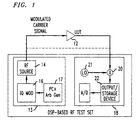
- FIGURE 1 illustrates a block schematic diagram of an apparatus 10, in accordance with the invention, for testing an RF device 12.
- the RF device 12 comprises a model ZHL-1042 J amplifier manufactured by Mini-Circuits, Inc., although many other types of RF devices may be tested by the test apparatus 10.
- the test apparatus 10 comprises an RF stimulus generator 13 that includes an RF signal source 14 that produces an RF signal that is digitally-modulated by a modulator 16 triggered by a modulation signal generated by a signal generator 17.
- the RF signal source 14 and modulator 16 collectively comprise a Rhodes & Shwarz model SMH U58 microwave synthesizer whereas the signal generator comprises the combination of a Rhodes & Shwarz model ADS dual arbitrary signal generator, operating under the control of a personal computer (not shown) that is programmed with Rhodes & Shwarz IQSIM software.
- the RF source 14 produces a digitally-modulated signal that is input to the RF device 12 under test.
- the RF device 12 In response to the RF stimulus signal, the RF device 12 generates a response that is received by a test receiver 18.
- the receiver 18 includes a mixer 20 for down-converting the RF response signal output by the RF device 12 to a lower frequency in accordance with a reference signal from a local oscillator 21.
- the receiver 20 includes an analog-to-digital converter 22 for digitizing the output signal of the down-converter 20, ultimately yielding the phase angle and magnitude of the down-converted, digitized RF response signal.
- the receiver 18 includes an output device, in the form of a display screen, and/or a storage device, such as a floppy disc drive, for displaying and/or retaining information generated by the receiver.
- the receiver comprises a Hewlett-Packard model HP 89440A Vector Signal Analyzer. This particular model Vector Signal Analyzer also has a mechanism for generating a digitally modulated test stimulus. However, for accuracy purposes, we have found it more desirable to employ the RF stimulus generator 13 as described previously.
- the test apparatus 10 may also include at least one processor, either in the form of the personal computer associated with the signal generator 17, or one or more separate stand-alone computers (not shown).
- the processor associated with the test apparatus 10 compares the phase angle and magnitude of the digitized, down-converted response signal of the RF device 12, as established by the receiver 18, to the phase angle and magnitude, respectively, of the digital stimulus produced by the RF source 14. By comparing the phase angle and magnitude of the digitized, down-converted signal of the RF device 12 to the phase angle and magnitude, respectively of the RF stimulus signal produced by the RF source 14, the processor associated with the test apparatus 10 establishes a set of transfer functions indicative of the operation of the RF device 12.
- BPSK Binary Phase Shift Key
- the receiver 18 samples the signal to produce 64 samples per binary phase shift key bit. Because the magnitude of the BPSK signal varies with time, the saturation characteristics of the RF device 12 can be extracted from the measurement made by the apparatus 10.
- and the phase angle ⁇ v in (t) of the input stimulus are first obtained. Typically, these values are obtained by feeding the output of the RF source 14 directly into the receiver 18 (as indicated by the dashed shunt across the RF device 12). Thereafter, the magnitude
- the gain g(t) of the RF device 12 can be established from the relationship:
- the gain g(t) and the phase shift ⁇ (t) given by eqs. (1) and (2), respectively, can be plotted against the digitally-modulated input stimulus signal magnitude
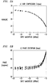
- FIGS. 2A and 2B show plots of the gain compression and phase distortion, respectively, for the model ZHL -1042 J RF amplifier 12 tested by the system of FIG. 1 using a 1 kilobit per second BPSK test stimulus.
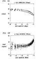
- FIGS 3A and 3B show plots of the gain compression and phase distortion, respectively, for the same amplifier using a 100 kilobit per second BPSK test stimulus.
- test technique of the invention has been described as utilizing BPSK signals, other modulation schemes may be employed. Indeed, any modulation scheme in which the magnitude of the stimulus varies over time will produce similar results. For example, Quadrature Shift Phase Keying (QPSK) modulation and ⁇ /4 Differential Quadrature Phase Shift Keying ( ⁇ /4 DQPSK) may also be employed.
- QPSK Quadrature Shift Phase Keying
- ⁇ /4 DQPSK Differential Quadrature Phase Shift Keying
- the technique of the present invention affords another distinct advantage. As compared to conventional test techniques that utilize an unmodulated RF carrier, the test technique of the invention allows for much more rapid testing.
- the foregoing discloses a technique for testing a RF device 12.
Abstract
Description
- This invention relates to a technique for testing an RF device, such as an RF amplifier, to assess its operating characteristics.
- There has been a tremendous surge in the development of wireless communications systems to meet the growing need of individuals and business to communicate information without being tethered to a wire or cable. The development of wireless communications systems has prompted the development of a wide variety of RF devices for use in such systems. The testing and characterization of RF devices has been a major factor in their development. In the past, such testing has been carried out by applying an unmodulated RF carrier to the device and then receiving the response generated by the device upon receipt of the carrier. The operating characteristics of the device are assessed in accordance with the phase and magnitude of the response signal, as compared to the phase and magnitude of the input carrier.
- RF testing in the manner described above incurs the disadvantage that the carrier applied to the device as the test stimulus often does not have the same characteristics as the signals supplied to the device under normal operating conditions. Modern radio systems typically employ digital modulation. Thus, the test results obtained by the use of an analog RF carrier as the test stimulus usually correlate poorly with the actual performance of the device under normal operating conditions, especially for non-linear devices.
- Thus, there is a need for a technique for testing an RF device that more accurately assesses the characteristics of the device under normal operating conditions.
- Briefly, in accordance with a preferred embodiment of the invention, a technique is provided for testing an RF device, such as an RF amplifier, and particularly, for testing its linearity. To test the RF device, a digitally-modulated RF stimulus signal, having a known, time-dependent phase angle and magnitude, is applied to the device to cause it to generate a modulated RF response signal. The RF response signal generated by the device following receipt of the digitally-modulated RF stimulus signal is down-converted in frequency and thereafter digitized. The phase angle and the magnitude of the digitized, down-converted response signal are determined and compared to the phase angle and magnitude, respectively, of the RF stimulus signal to establish the operating characteristics of the device.
- The test technique of the invention affords the advantage that the digitally-modulated stimulus signal closely resembles the digitally-modulated input signals that the device is likely to receive under normal operating conditions. Therefore, the operating characteristics of the device obtained by comparison of the phase angle and magnitude of the digitized, down-converted response signal to phase angle and magnitude, respectively, of the digitally-modulated stimulus signal more accurately reflect the true operation of the device.
-
- FIGURE 1 shows a block schematic diagram of a system, in accordance with the invention, for testing an RF device, such as an RF amplifier;
- FIGURES 2A and 2B show plots of the gain compression and phase distortion, respectively, for an RF device tested by the system of FIG. 1 using a 1 kilobit per second Binary Phase Shift Key (BPSK) test stimulus; and
- FIGURES 3A and 3B. show plots of the gain compression and phase distortion, respectively, for the RF device tested by the system of FIG. 1 using a 100 kilobit per second BPSK test stimulus.
- FIGURE 1 illustrates a block schematic diagram of an
apparatus 10, in accordance with the invention, for testing anRF device 12. In a preferred embodiment, theRF device 12 comprises a model ZHL-1042 J amplifier manufactured by Mini-Circuits, Inc., although many other types of RF devices may be tested by thetest apparatus 10. Thetest apparatus 10 comprises anRF stimulus generator 13 that includes anRF signal source 14 that produces an RF signal that is digitally-modulated by amodulator 16 triggered by a modulation signal generated by asignal generator 17. In a preferred embodiment, theRF signal source 14 andmodulator 16 collectively comprise a Rhodes & Shwarz model SMH U58 microwave synthesizer whereas the signal generator comprises the combination of a Rhodes & Shwarz model ADS dual arbitrary signal generator, operating under the control of a personal computer (not shown) that is programmed with Rhodes & Shwarz IQSIM software. - The
RF source 14 produces a digitally-modulated signal that is input to theRF device 12 under test. In response to the RF stimulus signal, theRF device 12 generates a response that is received by atest receiver 18. Thereceiver 18 includes amixer 20 for down-converting the RF response signal output by theRF device 12 to a lower frequency in accordance with a reference signal from alocal oscillator 21. Further, thereceiver 20 includes an analog-to-digital converter 22 for digitizing the output signal of the down-converter 20, ultimately yielding the phase angle and magnitude of the down-converted, digitized RF response signal. In addition, thereceiver 18 includes an output device, in the form of a display screen, and/or a storage device, such as a floppy disc drive, for displaying and/or retaining information generated by the receiver. In a preferred embodiment, the receiver comprises a Hewlett-Packard model HP 89440A Vector Signal Analyzer. This particular model Vector Signal Analyzer also has a mechanism for generating a digitally modulated test stimulus. However, for accuracy purposes, we have found it more desirable to employ theRF stimulus generator 13 as described previously. - In addition to the
RF stimulus generator 13, and thereceiver 18, thetest apparatus 10 may also include at least one processor, either in the form of the personal computer associated with thesignal generator 17, or one or more separate stand-alone computers (not shown). The processor associated with thetest apparatus 10 compares the phase angle and magnitude of the digitized, down-converted response signal of theRF device 12, as established by thereceiver 18, to the phase angle and magnitude, respectively, of the digital stimulus produced by theRF source 14. By comparing the phase angle and magnitude of the digitized, down-converted signal of theRF device 12 to the phase angle and magnitude, respectively of the RF stimulus signal produced by theRF source 14, the processor associated with thetest apparatus 10 establishes a set of transfer functions indicative of the operation of theRF device 12. - In testing the
RF device 12, we have found that a Binary Phase Shift Key (BPSK) signal, comprised of a either a 1 kilobit per second or 100 kilobit per second binary signal, superimposed on a 1.6 GHz carrier, provides a useful digitally-modulated stimulus signal for testing theRF device 12. In each case, thereceiver 18 samples the signal to produce 64 samples per binary phase shift key bit. Because the magnitude of the BPSK signal varies with time, the saturation characteristics of theRF device 12 can be extracted from the measurement made by theapparatus 10. - To measure the linearity characteristics of the
RF device 12, the magnitude |v in (t)| and the phase angle ∠ v in (t) of the input stimulus are first obtained. Typically, these values are obtained by feeding the output of theRF source 14 directly into the receiver 18 (as indicated by the dashed shunt across the RF device 12). Thereafter, the magnitude |v out (t)| and the phase angle ∠ v out (t) of the response generated by theRF device 12 are established. Once the magnitudes |v in (t)| and |v out (t)| and the phase angles ∠ v in (t) and ∠ v out (t) have been established, then the gain g(t) of theRF device 12 can be established from the relationship:

- The gain g(t) and the phase shift φ(t) given by eqs. (1) and (2), respectively, can be plotted against the digitally-modulated input stimulus signal magnitude |v in (t)| to obtain the gain compression and phase distortion, respectively, for the
RF device 12. FIGS. 2A and 2B show plots of the gain compression and phase distortion, respectively, for the model ZHL -1042J RF amplifier 12 tested by the system of FIG. 1 using a 1 kilobit per second BPSK test stimulus. FIGS 3A and 3B show plots of the gain compression and phase distortion, respectively, for the same amplifier using a 100 kilobit per second BPSK test stimulus. In practice, the measured gain compression and phase angle for theRF device 12 of FIG. 1 at low bit rates (e.g., 1 kilobit per second) have compared well to values obtained for these parameters by conventional RF testing using an analog carrier, demonstrating that the above-described digital test technique provides an accurate assessment of the operation of the device. From a comparison of the plots of FIGS 2A and 3A and 2B and 3B, this particular model amplifier is more linear at 100 kilobits per second than at 1 kilobit per second. Conventional RF testing with an unmodulated carrier would be incapable of revealing that theRF device 12 was more linear at higher bit rates. - Although the test technique of the invention has been described as utilizing BPSK signals, other modulation schemes may be employed. Indeed, any modulation scheme in which the magnitude of the stimulus varies over time will produce similar results. For example, Quadrature Shift Phase Keying (QPSK) modulation and π/4 Differential Quadrature Phase Shift Keying (π/4 DQPSK) may also be employed.
- In addition to providing test information unobtainable by conventional techniques, the technique of the present invention affords another distinct advantage. As compared to conventional test techniques that utilize an unmodulated RF carrier, the test technique of the invention allows for much more rapid testing.
- The foregoing discloses a technique for testing a
RF device 12.
Claims (9)
- A method for testing a RF electronic device, such as an amplifier or the like, comprising the step of:applying a digitally-modulated RF stimulus signal having a known time-dependent phase angle value and magnitude value, to the RF device to cause the RF device to generate a modulated RF response signal; CHARACTERIZED BY:down-converting the RF response signal;digitizing the down-converted RF response signal;establishing a phase angle value and magnitude value of the digitized, down-converted RF response signal; andcomparing the phase angle and magnitude values of the modulated RF stimulus signal to the phase angle and magnitude values, respectively, of the RF response signal to establish transfer functions for the RF device indicative of its operation.
- The method according to claim 1 wherein the digitally-modulated RF stimulus comprises a binary phase shift keyed signal.
- The method according to claim 2 wherein the binary phase shift keyed stimulus comprises a 1 kilobit per second binary signal superimposed on a 1.6 GHz carrier signal.
- The method according to claim 2 wherein the binary phase shift keyed stimulus signal comprises a 100 kilobit per second binary signal superposed on a 1.6 GHz carrier signal.
- The method according to claim 1 wherein a first transfer function (gain compression) is established in accordance with the ratio of the magnitude of the digitized, down-converted response signal to the magnitude of the digitally-modulated RF stimulus signal.
- The method according to claim 1 wherein a second transfer function (phase distortion) is established in accordance with the difference between the phase angle value of the digitized, down-converted response signal to the phase angle value of the digitally-modulated RF stimulus signal.
- Apparatus for testing an RF device comprising:means (13) for generating a digitally-modulated RF stimulus signal, having a known phase angle and magnitude, for input to the RF device to cause the RF device to generate an RF response signal; CHARACTERIZED BY:means (18) for receiving the RF response signal and for down-converting the RF response signal and digitizing the down-converted response signal; andmeans (17) for establishing the magnitude and phase angle of the digitized, down-converted response signal and for comparing the magnitude and phase angle of the digitized, down-converted response signal to the magnitude and phase angle, respectively, of the digitally-modulated RF stimulus signal to establish transfer functions indicative of the operation of the RF device.
- The apparatus according to claim 7 wherein the means for generating the digitally-modulated RF stimulus signal comprises:a source of RF signals (14); anda modulator (16) for modulating the signals from the source of RF signals.
- The apparatus according to claim 7 wherein the receiver includes:a down-converter (20, 21); andan analog-to-digital converter (22).
Applications Claiming Priority (2)
| Application Number | Priority Date | Filing Date | Title |
|---|---|---|---|
| US08/434,875 US5581190A (en) | 1995-04-29 | 1995-04-29 | Method and apparatus for testing RF devices |
| US434875 | 1995-04-29 |
Publications (2)
| Publication Number | Publication Date |
|---|---|
| EP0741301A2 true EP0741301A2 (en) | 1996-11-06 |
| EP0741301A3 EP0741301A3 (en) | 1996-11-20 |
Family
ID=23726061
Family Applications (1)
| Application Number | Title | Priority Date | Filing Date |
|---|---|---|---|
| EP96302685A Withdrawn EP0741301A3 (en) | 1995-04-29 | 1996-04-17 | Method and apparatus for testing RF devices |
Country Status (4)
| Country | Link |
|---|---|
| US (1) | US5581190A (en) |
| EP (1) | EP0741301A3 (en) |
| JP (1) | JPH09101334A (en) |
| CA (1) | CA2172321C (en) |
Cited By (2)
| Publication number | Priority date | Publication date | Assignee | Title |
|---|---|---|---|---|
| DE19750349A1 (en) * | 1996-11-14 | 1998-05-28 | Advantest Corp | Electrical mains supply analyser for components or equipment |
| EP1477819A1 (en) * | 2001-04-09 | 2004-11-17 | Taiyo Yuden Co., Ltd. | Method of measuring electromagnetic field intensity and device therefor,method of measuring electromagnetic field intensity distribution and device thereof, method of measuring current/voltage distribution and divice thereof |
Families Citing this family (12)
| Publication number | Priority date | Publication date | Assignee | Title |
|---|---|---|---|---|
| GB2314735B (en) * | 1996-06-28 | 2000-10-11 | Int Mobile Satellite Org | Storage and reproduction method and apparatus |
| US6628923B1 (en) * | 2000-05-03 | 2003-09-30 | Nokia Networks Oy | Adaptive phase and amplitude linearization method and apparatus |
| US7340219B2 (en) * | 2004-02-24 | 2008-03-04 | Texas Instruments Incorporated | Method and system for multisite RF transceiver testing |
| US7477875B2 (en) * | 2005-07-26 | 2009-01-13 | Texas Instruments Incorporated | Built in loop back self test in design or on test board for transceivers |
| US10404422B2 (en) | 2016-05-02 | 2019-09-03 | Keysight Technologies, Inc. | Measuring amplitude and phase response of measurement instrument with binary phase shift keying test signal |
| US11838076B2 (en) | 2021-01-28 | 2023-12-05 | Nucurrent, Inc. | Wireless power transmitter with in-band virtualized wired communications |
| US11418069B1 (en) | 2021-01-28 | 2022-08-16 | Nucurrent, Inc. | Wireless power transfer system with data-priority and power-priority transfer modes |
| US11271611B1 (en) | 2021-01-28 | 2022-03-08 | Nucurrent, Inc. | Wireless power transfer with in-band virtualized wired communications |
| US11316378B1 (en) | 2021-01-28 | 2022-04-26 | Nucurrent, Inc. | Wireless power receiver with in-band virtualized wired communications |
| US11483033B2 (en) | 2021-01-28 | 2022-10-25 | Nucurrent, Inc. | Wireless power transfer system with data versus power priority optimization |
| US11626756B1 (en) | 2021-10-15 | 2023-04-11 | Nucurrent, Inc. | Wireless power and data transfer system with out of band communications hand off |
| US11754618B2 (en) * | 2021-10-15 | 2023-09-12 | Nucurrent, Inc. | Testing device for electronic devices with in-band virtualized wired communications |
Citations (3)
| Publication number | Priority date | Publication date | Assignee | Title |
|---|---|---|---|---|
| US3938150A (en) * | 1974-06-25 | 1976-02-10 | The United States Of America As Represented By The Secretary Of The Navy | Microwave amplifier tube coherency test set |
| US4556841A (en) * | 1983-11-25 | 1985-12-03 | At&T Bell Laboratories | Measurement system for characterizing power amplifier and other device performance |
| US5089782A (en) * | 1989-03-22 | 1992-02-18 | Hewlett-Packard Company | Vector network analyzer for swept frequency harmonic and mixer conversion loss measurements using either an internal or external signal source |
Family Cites Families (4)
| Publication number | Priority date | Publication date | Assignee | Title |
|---|---|---|---|---|
| TW327488U (en) * | 1991-05-29 | 1998-02-21 | Video Tech Eng | Digital cordless telephone apparatus |
| US5179344A (en) * | 1991-06-21 | 1993-01-12 | Harris Corporation | Phase noise measurements utilizing a frequency down conversion/multiplier, direct spectrum measurement technique |
| US5337014A (en) * | 1991-06-21 | 1994-08-09 | Harris Corporation | Phase noise measurements utilizing a frequency down conversion/multiplier, direct spectrum measurement technique |
| JPH07147529A (en) * | 1993-06-28 | 1995-06-06 | Hitachi Ltd | Automatic frequency controller and control method using split band signal intensity measurement method |
-
1995
- 1995-04-29 US US08/434,875 patent/US5581190A/en not_active Expired - Lifetime
-
1996
- 1996-03-21 CA CA002172321A patent/CA2172321C/en not_active Expired - Fee Related
- 1996-04-17 EP EP96302685A patent/EP0741301A3/en not_active Withdrawn
- 1996-04-26 JP JP8106564A patent/JPH09101334A/en active Pending
Patent Citations (3)
| Publication number | Priority date | Publication date | Assignee | Title |
|---|---|---|---|---|
| US3938150A (en) * | 1974-06-25 | 1976-02-10 | The United States Of America As Represented By The Secretary Of The Navy | Microwave amplifier tube coherency test set |
| US4556841A (en) * | 1983-11-25 | 1985-12-03 | At&T Bell Laboratories | Measurement system for characterizing power amplifier and other device performance |
| US5089782A (en) * | 1989-03-22 | 1992-02-18 | Hewlett-Packard Company | Vector network analyzer for swept frequency harmonic and mixer conversion loss measurements using either an internal or external signal source |
Non-Patent Citations (5)
| Title |
|---|
| ELEKTRONIK, vol. 8, April 1989, DE, pages 136-139, XP002012274 B.SCHWEIGER: "Vektormodulations-Messtechnik" * |
| HEWLETT-PACKARD JOURNAL, vol. 44, no. 6, 1 December 1993, US, pages 47-57, 59, XP000422716 CUTLER R T ET AL: "RF VECTOR SIGNAL ANALYZER HARDWARE DESIGN" * |
| JEE JOURNAL OF ELECTRONIC ENGINEERING, vol. 29, no. 303, 1 March 1992, JP, pages 44-47, XP000298149 KANETO SASAKI: "WAVEFORM ANALYZER PERFORMS DIGITAL MODULATION" * |
| MICROWAVE JOURNAL, vol. 32, no. 3, 1 March 1989, US, page 129/130 XP000105875 SETTY R P N ET AL: "AUTOMATIC COMPRESSION MEASUREMENTS USING NETWORK ANALYZERS" * |
| PROCEEDINGS OF THE INSTRUMENTATION AND MEASUREMENT TECHNOLOGY CONFERENCE, ADVANCED TECHNOLOGIES IN I & M HAMAMATSU, MAY 10 - 12, 1994, vol. 2, 10 May 1994, US, pages 523-525, XP000509583 KUMAGAI M ET AL: "A SPECTRUM ANALYZER USING A HIGH SPEED HOPPING PLL SYNTHESIZER" * |
Cited By (4)
| Publication number | Priority date | Publication date | Assignee | Title |
|---|---|---|---|---|
| DE19750349A1 (en) * | 1996-11-14 | 1998-05-28 | Advantest Corp | Electrical mains supply analyser for components or equipment |
| DE19750349C2 (en) * | 1996-11-14 | 2000-05-18 | Advantest Corp | Network analyzer |
| EP1477819A1 (en) * | 2001-04-09 | 2004-11-17 | Taiyo Yuden Co., Ltd. | Method of measuring electromagnetic field intensity and device therefor,method of measuring electromagnetic field intensity distribution and device thereof, method of measuring current/voltage distribution and divice thereof |
| EP1477819A4 (en) * | 2001-04-09 | 2008-04-02 | Taiyo Yuden Kk | Method of measuring electromagnetic field intensity and device therefor,method of measuring electromagnetic field intensity distribution and device thereof, method of measuring current/voltage distribution and divice thereof |
Also Published As
| Publication number | Publication date |
|---|---|
| US5581190A (en) | 1996-12-03 |
| EP0741301A3 (en) | 1996-11-20 |
| CA2172321A1 (en) | 1996-10-30 |
| JPH09101334A (en) | 1997-04-15 |
| CA2172321C (en) | 1999-09-28 |
Similar Documents
| Publication | Publication Date | Title |
|---|---|---|
| US5581190A (en) | Method and apparatus for testing RF devices | |
| US4119964A (en) | Systems and methods for determining radio frequency interference | |
| KR100188045B1 (en) | Apparatus for compensatingof phase rotation in a final amplifier stage | |
| US6940263B2 (en) | Testing a transceiver | |
| WO2008036582A2 (en) | Active receiver detection and ranging | |
| US4140972A (en) | System for synchronizing synthesizers of communication systems | |
| WO2005053190A1 (en) | Signal interference measurement | |
| Cabot | Fundamentals of modern audio measurement | |
| US6526365B1 (en) | Low-power/wideband transfer function measurement method and apparatus | |
| US7031862B2 (en) | Apparatus and analysis method for determination of moisture in materials | |
| US3711764A (en) | Noise excited resonance apparatus | |
| US5949380A (en) | Antenna tester | |
| US4004230A (en) | Critical parameter receiver tester | |
| Ashley et al. | The measurement of noise in microwave transmitters | |
| US20040116080A1 (en) | Time resolved RF plasma impedance meter | |
| US6816559B1 (en) | FSK modulation transceiver | |
| EP0181701A1 (en) | Carrier to noise ratio measurement circuit | |
| US3913011A (en) | Method and apparatus for measuring conversion of amplitude modulation to phase modulation | |
| EP0314301B1 (en) | Apparatus and method for measuring the signal-to-noise ratio | |
| Riter | The effect of background noise on phase ranging measurements in urban vehicle monitoring systems | |
| JPH0771053B2 (en) | Burst position detector | |
| US3473113A (en) | Apparatus for measuring the phase distortions of a two-terminal network including differentiation and integration means | |
| Vael et al. | A controllable phase coherent pulsed RF signal generator for microwave network analyzer measurements | |
| Heutmaker et al. | Using digitally-modulated signals to measure the gain compression and phase distortion of a radio frequency amplifier | |
| US6731681B1 (en) | Method for determining the frequency instability noise from a source and a device for implementing the method |
Legal Events
| Date | Code | Title | Description |
|---|---|---|---|
| PUAI | Public reference made under article 153(3) epc to a published international application that has entered the european phase |
Free format text: ORIGINAL CODE: 0009012 |
|
| PUAL | Search report despatched |
Free format text: ORIGINAL CODE: 0009013 |
|
| AK | Designated contracting states |
Kind code of ref document: A2 Designated state(s): DE FR GB IT SE |
|
| AK | Designated contracting states |
Kind code of ref document: A3 Designated state(s): DE FR GB IT SE |
|
| 17P | Request for examination filed |
Effective date: 19970509 |
|
| 17Q | First examination report despatched |
Effective date: 20000331 |
|
| STAA | Information on the status of an ep patent application or granted ep patent |
Free format text: STATUS: THE APPLICATION IS DEEMED TO BE WITHDRAWN |
|
| 18D | Application deemed to be withdrawn |
Effective date: 20000811 |