EP0743684A2 - Thin film transistor with reduced channel length for liquid crystal displays - Google Patents
Thin film transistor with reduced channel length for liquid crystal displays Download PDFInfo
- Publication number
- EP0743684A2 EP0743684A2 EP96107792A EP96107792A EP0743684A2 EP 0743684 A2 EP0743684 A2 EP 0743684A2 EP 96107792 A EP96107792 A EP 96107792A EP 96107792 A EP96107792 A EP 96107792A EP 0743684 A2 EP0743684 A2 EP 0743684A2
- Authority
- EP
- European Patent Office
- Prior art keywords
- drain
- source
- metal
- electrode
- array
- Prior art date
- Legal status (The legal status is an assumption and is not a legal conclusion. Google has not performed a legal analysis and makes no representation as to the accuracy of the status listed.)
- Withdrawn
Links
- 239000010409 thin film Substances 0.000 title claims abstract description 33
- 239000004973 liquid crystal related substance Substances 0.000 title claims abstract description 31
- 229910052751 metal Inorganic materials 0.000 claims abstract description 101
- 239000002184 metal Substances 0.000 claims abstract description 101
- 239000000463 material Substances 0.000 claims abstract description 5
- 239000000758 substrate Substances 0.000 claims description 30
- 239000004065 semiconductor Substances 0.000 claims description 23
- 229910021417 amorphous silicon Inorganic materials 0.000 claims description 20
- 238000000151 deposition Methods 0.000 claims description 16
- 238000000059 patterning Methods 0.000 claims description 14
- 238000004519 manufacturing process Methods 0.000 claims description 11
- 150000002739 metals Chemical class 0.000 claims description 9
- 238000000034 method Methods 0.000 claims description 6
- 238000005530 etching Methods 0.000 claims description 2
- FGUUSXIOTUKUDN-IBGZPJMESA-N C1(=CC=CC=C1)N1C2=C(NC([C@H](C1)NC=1OC(=NN=1)C1=CC=CC=C1)=O)C=CC=C2 Chemical compound C1(=CC=CC=C1)N1C2=C(NC([C@H](C1)NC=1OC(=NN=1)C1=CC=CC=C1)=O)C=CC=C2 FGUUSXIOTUKUDN-IBGZPJMESA-N 0.000 claims 2
- 230000014759 maintenance of location Effects 0.000 abstract description 8
- 239000010408 film Substances 0.000 description 21
- 239000011651 chromium Substances 0.000 description 16
- 229910052581 Si3N4 Inorganic materials 0.000 description 11
- 230000003071 parasitic effect Effects 0.000 description 11
- HQVNEWCFYHHQES-UHFFFAOYSA-N silicon nitride Chemical compound N12[Si]34N5[Si]62N3[Si]51N64 HQVNEWCFYHHQES-UHFFFAOYSA-N 0.000 description 9
- 238000003491 array Methods 0.000 description 8
- 239000011159 matrix material Substances 0.000 description 8
- 150000002500 ions Chemical class 0.000 description 7
- 238000002048 anodisation reaction Methods 0.000 description 5
- BPUBBGLMJRNUCC-UHFFFAOYSA-N oxygen(2-);tantalum(5+) Chemical compound [O-2].[O-2].[O-2].[O-2].[O-2].[Ta+5].[Ta+5] BPUBBGLMJRNUCC-UHFFFAOYSA-N 0.000 description 5
- 238000002161 passivation Methods 0.000 description 5
- 230000009467 reduction Effects 0.000 description 5
- 229910001936 tantalum oxide Inorganic materials 0.000 description 5
- 230000007423 decrease Effects 0.000 description 4
- 238000000206 photolithography Methods 0.000 description 4
- QTBSBXVTEAMEQO-UHFFFAOYSA-N Acetic acid Chemical compound CC(O)=O QTBSBXVTEAMEQO-UHFFFAOYSA-N 0.000 description 3
- VYPSYNLAJGMNEJ-UHFFFAOYSA-N Silicium dioxide Chemical compound O=[Si]=O VYPSYNLAJGMNEJ-UHFFFAOYSA-N 0.000 description 3
- 230000008901 benefit Effects 0.000 description 3
- 229910052804 chromium Inorganic materials 0.000 description 3
- 230000008021 deposition Effects 0.000 description 3
- 230000006872 improvement Effects 0.000 description 3
- 238000002955 isolation Methods 0.000 description 3
- 238000001459 lithography Methods 0.000 description 3
- 229910052715 tantalum Inorganic materials 0.000 description 3
- GUVRBAGPIYLISA-UHFFFAOYSA-N tantalum atom Chemical compound [Ta] GUVRBAGPIYLISA-UHFFFAOYSA-N 0.000 description 3
- VYZAMTAEIAYCRO-UHFFFAOYSA-N Chromium Chemical compound [Cr] VYZAMTAEIAYCRO-UHFFFAOYSA-N 0.000 description 2
- RYGMFSIKBFXOCR-UHFFFAOYSA-N Copper Chemical compound [Cu] RYGMFSIKBFXOCR-UHFFFAOYSA-N 0.000 description 2
- ZOKXTWBITQBERF-UHFFFAOYSA-N Molybdenum Chemical compound [Mo] ZOKXTWBITQBERF-UHFFFAOYSA-N 0.000 description 2
- GRYLNZFGIOXLOG-UHFFFAOYSA-N Nitric acid Chemical compound O[N+]([O-])=O GRYLNZFGIOXLOG-UHFFFAOYSA-N 0.000 description 2
- NBIIXXVUZAFLBC-UHFFFAOYSA-N Phosphoric acid Chemical compound OP(O)(O)=O NBIIXXVUZAFLBC-UHFFFAOYSA-N 0.000 description 2
- RTAQQCXQSZGOHL-UHFFFAOYSA-N Titanium Chemical compound [Ti] RTAQQCXQSZGOHL-UHFFFAOYSA-N 0.000 description 2
- 229910052782 aluminium Inorganic materials 0.000 description 2
- 230000015572 biosynthetic process Effects 0.000 description 2
- XMPZTFVPEKAKFH-UHFFFAOYSA-P ceric ammonium nitrate Chemical compound [NH4+].[NH4+].[Ce+4].[O-][N+]([O-])=O.[O-][N+]([O-])=O.[O-][N+]([O-])=O.[O-][N+]([O-])=O.[O-][N+]([O-])=O.[O-][N+]([O-])=O XMPZTFVPEKAKFH-UHFFFAOYSA-P 0.000 description 2
- 238000005229 chemical vapour deposition Methods 0.000 description 2
- 229910052802 copper Inorganic materials 0.000 description 2
- 239000010949 copper Substances 0.000 description 2
- 239000008367 deionised water Substances 0.000 description 2
- 239000011521 glass Substances 0.000 description 2
- BHEPBYXIRTUNPN-UHFFFAOYSA-N hydridophosphorus(.) (triplet) Chemical compound [PH] BHEPBYXIRTUNPN-UHFFFAOYSA-N 0.000 description 2
- 239000012535 impurity Substances 0.000 description 2
- 239000012212 insulator Substances 0.000 description 2
- 239000000203 mixture Substances 0.000 description 2
- 238000012986 modification Methods 0.000 description 2
- 230000004048 modification Effects 0.000 description 2
- 229910052750 molybdenum Inorganic materials 0.000 description 2
- 239000011733 molybdenum Substances 0.000 description 2
- 229910017604 nitric acid Inorganic materials 0.000 description 2
- 229910052814 silicon oxide Inorganic materials 0.000 description 2
- 238000004544 sputter deposition Methods 0.000 description 2
- 229910052719 titanium Inorganic materials 0.000 description 2
- 239000010936 titanium Substances 0.000 description 2
- WFKWXMTUELFFGS-UHFFFAOYSA-N tungsten Chemical compound [W] WFKWXMTUELFFGS-UHFFFAOYSA-N 0.000 description 2
- 229910052721 tungsten Inorganic materials 0.000 description 2
- 239000010937 tungsten Substances 0.000 description 2
- 238000007740 vapor deposition Methods 0.000 description 2
- WUPHOULIZUERAE-UHFFFAOYSA-N 3-(oxolan-2-yl)propanoic acid Chemical compound OC(=O)CCC1CCCO1 WUPHOULIZUERAE-UHFFFAOYSA-N 0.000 description 1
- BUGBHKTXTAQXES-UHFFFAOYSA-N Selenium Chemical compound [Se] BUGBHKTXTAQXES-UHFFFAOYSA-N 0.000 description 1
- 229910045601 alloy Inorganic materials 0.000 description 1
- 239000000956 alloy Substances 0.000 description 1
- XAGFODPZIPBFFR-UHFFFAOYSA-N aluminium Chemical compound [Al] XAGFODPZIPBFFR-UHFFFAOYSA-N 0.000 description 1
- 229910000147 aluminium phosphate Inorganic materials 0.000 description 1
- 229910052980 cadmium sulfide Inorganic materials 0.000 description 1
- UHYPYGJEEGLRJD-UHFFFAOYSA-N cadmium(2+);selenium(2-) Chemical compound [Se-2].[Cd+2] UHYPYGJEEGLRJD-UHFFFAOYSA-N 0.000 description 1
- 230000015556 catabolic process Effects 0.000 description 1
- 230000003247 decreasing effect Effects 0.000 description 1
- 238000006731 degradation reaction Methods 0.000 description 1
- 229910021641 deionized water Inorganic materials 0.000 description 1
- 238000010586 diagram Methods 0.000 description 1
- 230000005684 electric field Effects 0.000 description 1
- 229910052732 germanium Inorganic materials 0.000 description 1
- GNPVGFCGXDBREM-UHFFFAOYSA-N germanium atom Chemical compound [Ge] GNPVGFCGXDBREM-UHFFFAOYSA-N 0.000 description 1
- 238000005259 measurement Methods 0.000 description 1
- JMOHEPRYPIIZQU-UHFFFAOYSA-N oxygen(2-);tantalum(2+) Chemical compound [O-2].[Ta+2] JMOHEPRYPIIZQU-UHFFFAOYSA-N 0.000 description 1
- 229920002120 photoresistant polymer Polymers 0.000 description 1
- 238000000623 plasma-assisted chemical vapour deposition Methods 0.000 description 1
- 238000012805 post-processing Methods 0.000 description 1
- 230000008569 process Effects 0.000 description 1
- 239000010453 quartz Substances 0.000 description 1
- 229910052594 sapphire Inorganic materials 0.000 description 1
- 239000010980 sapphire Substances 0.000 description 1
- 239000011669 selenium Substances 0.000 description 1
- 229910052711 selenium Inorganic materials 0.000 description 1
- 238000004904 shortening Methods 0.000 description 1
- HBMJWWWQQXIZIP-UHFFFAOYSA-N silicon carbide Chemical compound [Si+]#[C-] HBMJWWWQQXIZIP-UHFFFAOYSA-N 0.000 description 1
- 238000009751 slip forming Methods 0.000 description 1
- 229910052714 tellurium Inorganic materials 0.000 description 1
- PORWMNRCUJJQNO-UHFFFAOYSA-N tellurium atom Chemical compound [Te] PORWMNRCUJJQNO-UHFFFAOYSA-N 0.000 description 1
- XLYOFNOQVPJJNP-UHFFFAOYSA-N water Chemical compound O XLYOFNOQVPJJNP-UHFFFAOYSA-N 0.000 description 1
Images


Classifications
-
- H—ELECTRICITY
- H01—ELECTRIC ELEMENTS
- H01L—SEMICONDUCTOR DEVICES NOT COVERED BY CLASS H10
- H01L29/00—Semiconductor devices adapted for rectifying, amplifying, oscillating or switching, or capacitors or resistors with at least one potential-jump barrier or surface barrier, e.g. PN junction depletion layer or carrier concentration layer; Details of semiconductor bodies or of electrodes thereof ; Multistep manufacturing processes therefor
- H01L29/66—Types of semiconductor device ; Multistep manufacturing processes therefor
- H01L29/66007—Multistep manufacturing processes
- H01L29/66075—Multistep manufacturing processes of devices having semiconductor bodies comprising group 14 or group 13/15 materials
- H01L29/66227—Multistep manufacturing processes of devices having semiconductor bodies comprising group 14 or group 13/15 materials the devices being controllable only by the electric current supplied or the electric potential applied, to an electrode which does not carry the current to be rectified, amplified or switched, e.g. three-terminal devices
- H01L29/66409—Unipolar field-effect transistors
- H01L29/66477—Unipolar field-effect transistors with an insulated gate, i.e. MISFET
- H01L29/66742—Thin film unipolar transistors
- H01L29/6675—Amorphous silicon or polysilicon transistors
- H01L29/66765—Lateral single gate single channel transistors with inverted structure, i.e. the channel layer is formed after the gate
-
- H—ELECTRICITY
- H01—ELECTRIC ELEMENTS
- H01L—SEMICONDUCTOR DEVICES NOT COVERED BY CLASS H10
- H01L29/00—Semiconductor devices adapted for rectifying, amplifying, oscillating or switching, or capacitors or resistors with at least one potential-jump barrier or surface barrier, e.g. PN junction depletion layer or carrier concentration layer; Details of semiconductor bodies or of electrodes thereof ; Multistep manufacturing processes therefor
- H01L29/66—Types of semiconductor device ; Multistep manufacturing processes therefor
- H01L29/68—Types of semiconductor device ; Multistep manufacturing processes therefor controllable by only the electric current supplied, or only the electric potential applied, to an electrode which does not carry the current to be rectified, amplified or switched
- H01L29/76—Unipolar devices, e.g. field effect transistors
- H01L29/772—Field effect transistors
- H01L29/78—Field effect transistors with field effect produced by an insulated gate
- H01L29/786—Thin film transistors, i.e. transistors with a channel being at least partly a thin film
- H01L29/78696—Thin film transistors, i.e. transistors with a channel being at least partly a thin film characterised by the structure of the channel, e.g. multichannel, transverse or longitudinal shape, length or width, doping structure, or the overlap or alignment between the channel and the gate, the source or the drain, or the contacting structure of the channel
Definitions
- This invention relates to an array of thin film transistors, each transistor having a reduced channel length. More particularly, this invention relates to an array of thin film transistors (TFTs) adapted to be used in an LCD, each TFT having a reduced channel length so as to limit gate-source capacitance which in turn reduces pixel flickering and image retention thereby improving the viewing characteristics of the LCD.
- TFTs thin film transistors
- Active matrix liquid crystal display (AMLCD) devices are typically composed of a matrix of liquid crystal pixels arranged horizontally in rows and vertically in columns. Such devices include first and second opposing polarizers, a liquid crystal layer disposed between the polarizers, and transparent electrodes mounted on opposite sides of the liquid crystal (LC) layer so as to selectively energize same in order to create an image for a viewer.
- AMLCD Active matrix liquid crystal display
- Such active matrix displays generally include X and Y (or row and column) address lines which are vertically and horizontally spaced apart and cross at an angle to one another thereby forming a plurality of crossover points. Associated with each crossover point is an element to be selectively addressed. These elements in many instances are liquid crystal display pixels or alternatively the memory cells of an electronically addressable memory array.
- isolation device e.g. a thin film transistor
- the isolation devices permit the individual pixels to be selectively addressed by the application of suitable potentials between respective pairs of the X and Y address lines.
- Amorphous silicon (a-Si) TFTs have found wide usage for isolation devices in such LCD arrays.
- Thin film transistors (TFTs) formed from deposited semiconductors such as amorphous silicon alloys are ideally suited for such applications because they exhibit a high dark resistivity and, therefore, have low OFF state currents.
- the reverse leakage currents are low so that high on-to-off current ratios are made possible for effectively isolating non-addressed array pixels from the pixels being addressed.
- TFTs thin film transistors
- TFTs generally include substantially co-planar source and drain electrodes, a semiconductor material between the source and drain electrodes, and a gate electrode in proximity to the semiconductor but electrically insulated therefrom by a gate insulator.
- Current flow through the TFT between the source and drain is controlled by the application of voltage to the gate electrode.
- the voltage to the gate electrode produces an electric field which accumulates a charged region near the semiconductor-gate insulator interface. This charged region forms a current conducting channel in the semiconductor through which current is conducted.
- the source and drain electrodes in conventional TFT arrays are typically deposited and patterned on a substrate by way of either flat panel steppers or large area scanning projection aligners in order to define a channel length and width between the source and drain.
- Large area scanning projection aligners using a single large area mask cost about half as much as flat panel steppers, and have about twice the manufacturing throughput as the steppers.
- Conventional scanning projection aligners typically have a resolution of from about 4 to 6 ⁇ m while conventional flat panel steppers typically have a resolution of from about 3 to 4 ⁇ m. In consideration of cost and manufacturing throughput, it is clear that it would be desirable to utilize scanning projection aligners as opposed to flat panel steppers so as to decrease manufacturing costs and increase throughput.
- TFT channel lengths smaller than those achievable with certain scanning projection aligners are often desirable for reasons to be discussed below.
- TFT source-drain channel lengths of about 6 ⁇ m can be obtained with scanning projection aligners.
- the resulting channel lenth of a TFT is typically larger or longer than the minimum feature size of the aligner used due to overetching of the source and drain.
- the overetch is typically about 1 ⁇ m so that a designed channel length of 4 ⁇ m ends up as a post-processing TFT channel length of about 6 ⁇ m.
- the channel width must be increased in order to maintain the same ON current because the TFT ON current is proportional to W/L where "W" is the channel width and "L" is the channel length.
- Pixel voltage shift ⁇ V p in thin film transistor LCDs after switching off the gate electrode is proportional to the gate-source capacitance (C gs ) of the thin film transistor.
- C gs gate-source capacitance
- An effective way to reduce C gs is by shortening the channel length of the TFT.
- the channel width "W" can be reduced proportionally so as to decrease C gs because C gs is proportional to the channel width.
- FIG. 1 is a side elevational cross-sectional view of prior art linear thin film transistor (TFT) 1.
- TFT linear thin film transistor
- a plurality of TFTs 1 are typically arranged on transparent insulating substrate 3 in the form of a matrix array in AMLCD applications.
- Each TFT 1 includes gate electrode 5 connected to a gate line (not shown) extending in the row direction, drain electrode 7 connected to a drain line (not shown) extending the column direction, and source electrode 9 connected to transparent pixel electrode 11 independently formed in an area surrounded by the gate and drain lines.
- Pixel electrode 11 operates in conjunction with an opposing electrode on the other side of the liquid crystal layer (not shown) so as to selectively drive the pixel enabling the respective polarizers to transmit or absorb light rays in order to create an image for the viewer.
- a TFT electrode, to which a data signal is supplied, will be referred to hereinafter as a drain electrode.
- gate electrode 5 is formed on clear substrate 3.
- Drain and source electrodes 7 and 9 respectively are formed on semiconductor film 15. The linear shaped source and drain electrodes are separated from one another by a predetermined distance forming channel length 17. Drain and source electrodes 7 and 9 respectively utilize contact layers 7a and 9a, and drain-source metal layers 7b and 9b, and are electrically connected to semiconductor film 15.
- TFT 1 is manufactured using, for example, a conventional scanning projection aligner to position the source and drain electrodes on substrate 3, the resulting channel length 17 of TFT 1 cannot be made as small as desired thereby resulting in an undesirably high parasitic capacitance (C gs ).
- C gs parasitic capacitance
- High parasitic capacitance values for TFTs are undesirable as set forth above because they tend to cause pixel flickering, image retention, and gray scale non-uniformity.
- the parasitic capacitance of a TFT is decreased, the pixel voltage shift when the gate is switched off becomes smaller. As the pixel voltage shift decreases, it becomes easier to compensate the top plate voltage to eliminate DC components for all gray levels and across the entire display area.
- Flickering results from a small DC component across the pixel electrodes spanning the liquid crystal layer. Pure AC voltage across the electrodes is ideal. By reducing the parasitic capacitance, the DC component across the pixel electrodes can be substantially eliminated or reduced thereby greatly reducing pixel flickering, electrochemical degradation, and image retention of the LC material.
- a liquid crystal display including a TFT array wherein the TFTs in the array have reduced parasitic capacitances and are cost effective to manufacture.
- Such TFTs are achievable in accordance with this invention by reducing the obtainable TFT channel lengths so as to decrease parasitic capacitance values in order to reduce flickering, image retention, and gray scale non-uniformity of the display. It would also be desirable if TFT channel lengths smaller than those allowed by the feature size of the manufacturing equipment could be obtained so as to reduce costs.
- this invention fulfills the above-described needs in the art by providing a liquid crystal display having an array of thin film transistors, the liquid crystal display comprising:
- This invention further fulfills the above-described needs in the art by providing a thin film transistor comprising:
- This invention still further fulfills the above-described needs in the art by providing a method of making a thin film transistor comprising the steps of:
- Figure 1 is a side elevation cross-sectional view of a prior art linear-type TFT.
- Figure 2 is a side elevational cross-sectional view of a linear TFT according to an embodiment of this invention.
- Figure 3 is a top view illustrating the linear TFT of Figure 2.
- Figure 4 is a diagram of a TFT array including a plurality of the Figure 2 TFTs connected to respective gate and drain address lines.
- Figure 5 is a partial cut-away perspective view of an active matrix liquid crystal display including a plurality of the Figure 2 TFTs arranged in an array so as to act as switching devices for the pixels.
- Figure 6 is a top view illustrating the source and drain electrodes of a TFT cross-sectionally according to a ring-shaped TFT embodiment of this invention.
- Figure 7 is a side cross-sectional view of the Figure 6 ring-shaped TFT with reduced annular channel length.
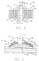
- FIGS 2-3 are side cross-sectional and top views respectively of linear thin film transistor (TFT) 21 according to an embodiment of this invention.
- TFT 21 has a channel length L 2 shorter than that allowed by the feature size of the lithography (e.g. when a scanning projection aligner is used) used for patterning drain electrode 23 and source electrode 25.
- Source electrode 25 is connected to LCD pixel electrode 51 (see Figures 4-5) so as to permit TFT 21 to selectively energize a corresponding pixel in order to provide image data to a viewer, TFT 21 effectively functioning as a switch for the corresponding LCD pixel.
- An array of TFTs 21 is provided in a typical active matrix liquid crystal display so as to correspond with an array of pixel electrodes 51.
- TFT 21 includes transparent substrate 27 (e.g. made of glass), metal gate electrode 29, gate insulating layer 31, semiconductor layer 33 (e.g. amorphous silicon), contact layer 39, drain electrode 23, and source electrode 25.
- transparent substrate 27 e.g. made of glass
- metal gate electrode 29 e.g. made of glass
- gate insulating layer 31 e.g. amorphous silicon
- semiconductor layer 33 e.g. amorphous silicon
- contact layer 39 e.g. amorphous silicon
- drain electrode 23 e.g. amorphous silicon
- Drain electrode 23 includes first deposited metal drain layer 35 (e.g. Cr) and second deposited metal drain layer 37 (e.g. Mo), with contact film 39 (e.g. amorphous silicon doped with an impurity such as phosphorous) disposed between semiconductor layer 33 and first deposited metal drain layer 35.
- Drain layers 35 and 37 are offset with respect to one another by an amount ⁇ L so that layer 37 is disposed closest to and defines TFT channel 41 while first deposited drain layer 35 is located in a spaced relation from channel 41.
- Drain metals 35 and 37 are deposited in separate steps (e.g. via conventional photolithographic methods) so as to have substantially equivalent lengths according to certain embodiments of this invention.
- the first-deposited source-drain metal layer 35, 43 e.g. Cr
- Source electrode 25 includes first deposited metal layer 43 (e.g. Cr) and second deposited metal layer 45 (e.g. Mo). Source layers 43 and 45 are deposited and patterned on substrate 27 in separate steps over top of gate 29, gate insulating layer 31, and semiconductor layer 33 by way of conventional photolithographic techniques according to certain embodiments of this invention. Source layers 43 and 45 are offset with respect to one another so that first deposited metal layer 43 is closest to and defines TFT channel 41 in conjunction with second deposited drain metal layer 37. Accordingly, second deposited source metal layer 45 is spaced from TFT channel 41 by an offset amount ⁇ L. First deposited drain layer 35 is also spaced from channel 41 by an offset amount ⁇ L according to certain embodiments of this invention with these two ⁇ L values being either substantially the same or different according to different embodiments of this invention.
- first deposited metal layer 43 e.g. Cr
- second deposited metal layer 45 e.g. Mo
- Source metal layer 43 and drain metal layer 35 are deposited and patterned in the same photolithographic step and are made of the same metal (e.g. Cr) according to certain embodiments, with second source-drain metal layers 45 and 37 (e.g. Mo) being then deposited over top of layers 43 and 35 in a second photolithographic step so that the second deposited source-drain layers are offset an amount ⁇ L from the first deposited layers 43 and 35.
- second source-drain metal layers 45 and 37 e.g. Mo
- TFT 21 has a channel length L 2 shorter than that allowed by the feature size of the lithography used for patterning source 25 and drain 23. Because the offset ⁇ L (e.g. from about 1 to 3 ⁇ m) may vary across the substrate, different TFTs in the array may have different channel lengths L 2 . The reduction of C gs across the array clearly overshadows this variation tendency.
- ⁇ L e.g. from about 1 to 3 ⁇ m
- first source-drain metal layers 35 and 43 are deposited and patterned, second layers 37 and 45 are then deposited and patterned (offset to the first layers) using the same (or different in some embodiments) channel length L 1 over top of layers 35 and 43, the result being TFT channel length L 2 which is shorter than the feature size of the lithography used for depositing and patterning the source and drain electrodes.
- L 1 is the length or gap defined between first-deposited layers 35 and 43 (or layers 37 and 45).
- ⁇ L is the amount the second deposited source-drain layers are offset laterally with respect to the first deposited source-drain metal layers.
- channel length L 2 is defined by the originally patterned channel length size L 1 minus the offset amount ⁇ L.
- Gate electrode 29 consisting essentially of a metal film (e.g. Ta) having a thickness of about 1,000-5,000 ⁇ , most preferably about 2,500 ⁇ , is deposited by means of sputtering or vapor deposition on the cleaned top surface of transparent insulating substrate 27.
- Insulating substrate 27 may be made of glass, quartz, sapphire, or the like.
- the metal film is then patterned by photolithography or the like to form gate electrode 29.
- the Ta layer 29 (when originally 2,500 ⁇ thick) is about 1,800 ⁇ thick and the created TaO layer is about 1,600 ⁇ thick.
- layer 31 in Figure 2 is made up of both the TaO layer and the silicon nitride layer.
- Other metals from which gate electrode 29 may be made include Cr, Al, titanium, tungsten, copper, and combinations thereof.
- Gate insulating film 31 (e.g. SiN or Si 3 N 4 ) is then formed on the surface of substrate 27 by plasma enhanced chemical vapor deposition (CVD) or the like so as to have a thickness of about 2,000-3,000 ⁇ (preferably either about 2,000 ⁇ or 3,000 ⁇ ) and cover gate electrode 29. Silicon nitride, silicon oxide, tantalum oxide, or combinations thereof may be used to form gate insulating film or layer 31.
- semiconductor layer 33 made of amorphous silicon (a-Si) or the like and contact films 39 also made of amorphous silicon (a-Si) doped with an impurity at high concentration (e.g. about 1% phosphorous) are continuously formed or stacked by plasma chemical vapor deposition or the like on gate insulating film 31 so that layer 33 is disposed between film 31 and contact films 39.
- Semiconductor layer 33 is deposited to a thickness of, for example, about 2,000 ⁇ while contact layers 39 are deposited to a thickness of, for example, about 500 ⁇ .
- Semiconductor layer 31 may be from about 1,000 ⁇ to 4,000 ⁇ thick while doped layers 39 may be from about 200 ⁇ to 1,000 ⁇ thick according to certain embodiments of this invention.
- Semiconductor layer 33 and contact films 39 are patterned by photolithography or the like so as to cover a portion above gate electrode 29.
- amorphous silicon amorphous silicon carbide, tellurium, selenium, germanium, cadmium sulfide, cadmium selenide, or the like may be used a material for semiconductor layer 33 and contact films 39.
- the first source-drain metal layer (which results in layers 35 and 43) having a thickness of from about 500-5,000 ⁇ (preferably from about 500 to 2,000 ⁇ , and most preferably about 1,000 ⁇ thick) is then formed on the entire surface extant by vapor deposition, sputtering, or the like so as to cover contact films 39.
- This metal (e.g. Cr) film is then patterned by photolithography, etching, or the like in order to remove the metal layer and contact films 39 at channel portion 41 thereby forming drain metal layer 35 and source metal layer 43 above gate electrode 29.
- First deposited drain and source layers 35 and 43 respectively are separated by a channel length L 1 after patterning.
- Layers 35 and 43 are made of chromium (Cr) according to certain embodiments of this invention.
- Other metals which may be used include titanium, aluminum, tungsten, tantalum, copper, molybdenum (Mo), or the like.
- layers 37 and 45 are deposited and patterned from a single metal layer using the same feature size channel length but offset by an amount ⁇ L from the first-deposited layers 35 and 43.
- a single metal (e.g. Mo) layer from about 1,000 ⁇ to 7,000 ⁇ thick (preferably about 5,000 ⁇ of Mo) is deposited and patterned to form drain metal 37 and source metal 45 which are separated by an amount L 1 .
- second-deposited source-drain metal layers 37 and 45 are made of Mo so that the etchant for layers 37 and 45 (Mo) does not etch first-deposited layers 35 and 43 (Cr).
- the etchant for Cr is a commonly used mixture of ceric ammonium nitrate and nitric acid in deionised water
- the etchant for Mo second deposited source-drain metal
- Such etchants are used for the two offset source-drain layers so that the etchant for the Mo does not etch the Cr.
- the same mask can be used for both metal layer patterning steps.
- possible overlay error which could have occurred if different masks were used is reduced.
- the offset of the two source-drain metals can be automatically programmed.
- a passivation layer (e.g. SiN or Si 3 N 4 ) is deposited over top of the source and drain.
- the passivation layer (not shown in Figures 2-3, but discussed and shown with respect to Figure 7) is then removed only in the pixel electrode 51 areas.
- the passivation layer may be from about 2,000 to 4,000 ⁇ thick, most preferably about 2,000 ⁇ thick according to certain embodiments of this invention.
- the pixel electrode layer (e.g. ITO) 51 may be deposited on substrate 27 at any one of a number of possible positions during the manufacturing of TFT 21. Firstly, the ITO pixel electrode layer (not shown in Figures 2-3 but discussed and shown with respect to Figures 4, 5, and 7) may be deposited over top of the passivation layer and thereafter patterned to form pixel electrode members 51, and connectors 63 which are affixed to source electrode 25. A via or aperture may be defined in the passivation layer which allows the ITO pixel electrode layer (or connector 63) to make electrical contact with source 25.
- the ITO pixel electrode layer may be deposited after the depositing of silicon nitride layer 31 on substrate 27 but before the deposition of the source-drain metals. Again, the ITO pixel electrode layer is in electrical contact with source 25.
- the ITO pixel electrode layer may be deposited underneath of silicon nitride layer 31 directly on substrate 27 with a via being defined in layer 31 so as to allow the ITO layer to make electrical contact with source 25.
- the ITO layer is patterned so it does not make electrical contact with gate electrode 29.
- the reduction of the TFT channel length to a value L 2 from a value L 1 combined with the reduction of the channel width reduces the parasitic capacitance (C gs ) so as to reduce pixel flickering, image retention, and gray level non-uniformity in LCD operations.
- the reduction in channel width is the major contributor to the reduction in C gs(ON) .
- Exemplary ⁇ L values according to certain embodiments of this invention are from about 2 to 3 ⁇ m while exemplary channel length values L 2 are from about 2 to 4 ⁇ m when conventional photolithographic features sizes (on scanning projection aligners or flat panel steppers, for example) of about 6 ⁇ m are used.
- FIG. 4 illustrates an array of thin film transistors (TFTs 21) which act as switching elements for LCD pixel electrodes 51.
- TFTs 21 are electrically connected to a row address line 53 and a column address line 55.
- row address lines 53 i.e. gate lines
- column address lines 55 i.e. drain lines
- Another advantage associated with certain embodiments of this invention is that the use of first and second-deposited source-drain metals allows for full redundancy for column lines 55 so that the incidence of partial open column lines is reduced thereby improving manufacturing yield.
- FIG. 5 is a perspective partially cut-away view of an active matrix liquid crystal display including an array of TFTs 21 which act as switching elements for pixel electrodes 51.
- the AMLCD is made up of liquid crystal layer 57 sandwiched between substrate 27 and substrate 61.
- Common electrode 59 is positioned adjacent liquid crystal layer 57 and is located between LC layer 57 and substrate 61.
- TFTs 21 are connected to pixel electrodes 51 (e.g. made of transparent ITO) by way of conductive ITO connecting portions 63.
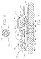
- FIGS 6 and 7 are top and side cross-sectional views respectively of a ring-shaped TFT 71 according to another embodiment of this invention.
- Ring-shaped TFT 71 includes round or annular source electrode 73 which is substantially completely surrounded by annular drain electrode 75 so as to form annular TFT channel 77.
- Gate electrode 79 is first formed on transparent substrate 27. Following the depositing and patterning of metal (e.g. Ta) gate electrode 79, gate insulating layer (e.g. silicon nitride) 81 is deposited on substrate 27 over top of gate electrode 79. Then, semiconductor layer 83 (e.g. amorphous silicon) and contact layers 85 (e.g. doped amorphous silicon) are formed on gate insulating layer 81 and substrate 27.
- metal e.g. Ta
- gate insulating layer e.g. silicon nitride
- semiconductor layer 83 e.g. amorphous silicon
- contact layers 85 e.g. doped amorphous silicon
- a first source-drain metal layer (which results in layers 73 and 89) is deposited on substrate 27 over top of layers 81 and 83.
- the first source-drain metal layer e.g. Cr
- the first source-drain metal layer is patterned via conventional photolithography so as to form source electrode 73 and annular first deposited drain metal layer 89.
- Annular drain layer 89 circumferentially surrounds or encompasses source layer 73 so as to reduce the parasitic capacitance of the TFT.
- the channel length L 1 of the TFT is defined by the lateral distance between the outer diameter of source electrode 73 and the inner diameter of drain electrode 89.
- a second metal (e.g. Mo) layer is deposited over top of the first metal layer and patterned so as to form second-deposited drain layer 91 which is formed over top of and offset relative to first-deposited drain layer 89.
- second-deposited drain layer 91 is offset with respect to first-deposited layer 89, the resulting channel length L 2 of the TFT is reduced by the amount of offset ⁇ L as in the previous embodiment.
- the resulting TFT channel length L 2 is again equal to L 1 - ⁇ L where ⁇ L is the amount of lateral offset between layers 89 and 91 and L 1 is the channel length defined between first-deposited layers 73 and 89.
- TFTs 21 An array of linear-type TFTs 21 (see Figures 2-3) was manufactured and tested as follows.
- the TFTs each included substrate 27, tantalum (Ta) gate 29, silicon nitride insulating film 31, amorphous silicon (a-Si) semiconductor layer 33, amorphous silicon doped contact films 39, chromium (Cr) first-deposited source-drain metal layers 35 and 43, and molybdenum (Mo) second-deposited source-drain metal layers 37 and 45 as set forth in Figures 2-3.
- the second deposited source-drain metal layers were laterally offset an amount ⁇ L from the first-deposited source-drain metal layers as shown in Figures 2-3.
- the offset amount for each TFT 21 was about 2.5 to 3.0 ⁇ m.
- the TFTs in the array each had a channel 41 length L 2 of about 3 ⁇ m and a channel 41 width of about 24 ⁇ m.
- the thickness of silicon nitride layer 31 was about 2,000 ⁇ and the thickness of Ta gate 29 was about 2,500 ⁇ .
- the thickness of Cr source-drain layers 35 and 43 was about 1,000 ⁇ and the thickness of Mo source-drain metal layers 37 and 45 was about 5,000 ⁇ . Measurements obtained from this TFT 21 array are set forth below in Tables 1 and 2 where the TFTs of this example (TFT Array #2) are compared to two different (TFT Array #s 1 and 3) prior art linear-type TFT arrays. This concludes this Example.
- TFT Array #1 (prior art) 24 ⁇ m 6 ⁇ m 2,000 ⁇ 0 ⁇ No offset No anodization TFT Array #2
- Example 1 24 ⁇ m 3 ⁇ m 2,000 ⁇ 0 ⁇ Short-channel TFT No anodization TFT Array #3 (prior art) 24 ⁇ m 6 ⁇ m 2,000 ⁇ 1,600 ⁇ Standard process TABLE #2
- Substrate # TFT Loc I OFF [pA] I ON [ ⁇ A] V th [V] ⁇ cm 2 /V-s C gs(OFF) [fF] C gs(ON) [fF] C gd(OFF ) [fF] C gd(ON) [fF] TFT Array #1 (prior art) BR 0.08 12.7 1.06 1.16 28 60 30 64 TR 0.16 12.0 1.60 1.01 - - - TL (1) 0.03 12.4 1.47
- TFTs according to the Figure 2-3 embodiment of this invention were compared to TFTs from prior art arrays (TFT Array #1 and TFT Array #3).
- Each array included a plurality of TFTs all having channel widths of about 24 ⁇ m.
- the TFTs of Arrays #s 1 and 3 had channel lengths of about 6 ⁇ m while the TFTs of Array #2 (see Example 1) had channel lengths of about 3 ⁇ m.
- the thickness of silicon nitride layer 31 in all three arrays was about 2,000 ⁇ .
- TFT Array #3 anodization took place so as to form a tantalum oxide (TaO) layer about 1,600 ⁇ thick where the gate electrode was, of course, formed of tantalum.
- TFT Array #s 1 and 2 no anodization step was performed. Therefore, the thickness of the TaO layer in Array #s 1 and 2 was 0 ⁇ . Only one source-drain metal (Mo) was used in the prior art arrays.
- the term “BR” refers to a TFT on the "bottom right” of substrate 27. Accordingly, the term “TR” refers to a TFT on the "top right” of substrate 27, the term “TL” refers to a TFT on the "top left” portion of substrate 27, and the term “BL” refers to a TFT on the "bottom left” portion of substrate 27.
- the short-channel TFTs (Array #2) according to the different embodiments of this invention realize certain advantages over the prior art (TFT Array #s 1 and 3) TFTs.
- the often-described figure of merit for a thin film transistor (TFT) is I ON /C gs(ON) .
- the TFT figure of merit is the ON current divided by gate-source capacitance in the ON state. It is desirable to increase this figure of merit to as high a level as possible.
- the ON current (I ON ) is the ever important parameter used in determining how fast a pixel will charge up.
- C gs(ON) is the gate-source capacitance in the TFT ON state and determines the pixel voltage drop or shift after switching off the gate.
- I ON /C gs(ON) for the top left TFT of Array #2 was measured to be about 0.374.
- I ON /C gs(ON) for the top left (1) TFT in prior art Array #1 was measured to be only about 0.217.
- the figure of merit I ON /C gs(ON) for the top left measured TFT in Array #3 was measured to be only about 0.143.
- the advantages of the TFTs according to the Figure 2-3 embodiment of this invention is also illustrated by the measured C gs(ON) values set forth in TABLE 2.
- the measured values indicate that the TFTs in Array #2 have reduced parasitic capacitance values with respect to corresponding TFTs in prior art Array #1 and prior art Array #3.
- the bottom right TFT in Array #2 had a C gs(ON) of 46 fF while the bottom right TFT in prior art Array #1 had a C gs(ON) value of 60 fF.
- the bottom right TFT in prior art Array #3 (anodized) had a C gs(ON) value of 50 fF.
Abstract
Description
- This invention relates to an array of thin film transistors, each transistor having a reduced channel length. More particularly, this invention relates to an array of thin film transistors (TFTs) adapted to be used in an LCD, each TFT having a reduced channel length so as to limit gate-source capacitance which in turn reduces pixel flickering and image retention thereby improving the viewing characteristics of the LCD.
- Active matrix liquid crystal display (AMLCD) devices are typically composed of a matrix of liquid crystal pixels arranged horizontally in rows and vertically in columns. Such devices include first and second opposing polarizers, a liquid crystal layer disposed between the polarizers, and transparent electrodes mounted on opposite sides of the liquid crystal (LC) layer so as to selectively energize same in order to create an image for a viewer.
- Electronic matrix arrays find considerable application in AMLCDs. Such active matrix displays generally include X and Y (or row and column) address lines which are vertically and horizontally spaced apart and cross at an angle to one another thereby forming a plurality of crossover points. Associated with each crossover point is an element to be selectively addressed. These elements in many instances are liquid crystal display pixels or alternatively the memory cells of an electronically addressable memory array.
- Some form of isolation device (e.g. a thin film transistor) is generally associated with each array element or pixel. The isolation devices permit the individual pixels to be selectively addressed by the application of suitable potentials between respective pairs of the X and Y address lines.
- Amorphous silicon (a-Si) TFTs have found wide usage for isolation devices in such LCD arrays. Thin film transistors (TFTs) formed from deposited semiconductors such as amorphous silicon alloys are ideally suited for such applications because they exhibit a high dark resistivity and, therefore, have low OFF state currents. The reverse leakage currents are low so that high on-to-off current ratios are made possible for effectively isolating non-addressed array pixels from the pixels being addressed.
- Structurally, thin film transistors (TFTs) generally include substantially co-planar source and drain electrodes, a semiconductor material between the source and drain electrodes, and a gate electrode in proximity to the semiconductor but electrically insulated therefrom by a gate insulator. Current flow through the TFT between the source and drain is controlled by the application of voltage to the gate electrode. The voltage to the gate electrode produces an electric field which accumulates a charged region near the semiconductor-gate insulator interface. This charged region forms a current conducting channel in the semiconductor through which current is conducted.
- The source and drain electrodes in conventional TFT arrays are typically deposited and patterned on a substrate by way of either flat panel steppers or large area scanning projection aligners in order to define a channel length and width between the source and drain. Large area scanning projection aligners using a single large area mask cost about half as much as flat panel steppers, and have about twice the manufacturing throughput as the steppers. Conventional scanning projection aligners typically have a resolution of from about 4 to 6 µm while conventional flat panel steppers typically have a resolution of from about 3 to 4 µm. In consideration of cost and manufacturing throughput, it is clear that it would be desirable to utilize scanning projection aligners as opposed to flat panel steppers so as to decrease manufacturing costs and increase throughput.
- TFT channel lengths smaller than those achievable with certain scanning projection aligners are often desirable for reasons to be discussed below. Typically, TFT source-drain channel lengths of about 6 µm can be obtained with scanning projection aligners. However, it is often desirable to achieve channel lengths less than 6 µm.
- The resulting channel lenth of a TFT is typically larger or longer than the minimum feature size of the aligner used due to overetching of the source and drain. In the case of Mo source-drain metal, for example, the overetch is typically about 1 µm so that a designed channel length of 4 µm ends up as a post-processing TFT channel length of about 6 µm. As a result of this, the channel width must be increased in order to maintain the same ON current because the TFT ON current is proportional to W/L where "W" is the channel width and "L" is the channel length. Accordingly, there exists a need in the art for a thin film transistor (and method of manufacturing same) having a channel length smaller than that allowed by the minimum feature size or resolution of the equipment used to manufacture the TFT so that, for example, about a 4 µm channel length or less can be achieved using low-cost equipment such as scanning projection aligners (instead of flat panel steppers).
- Smaller TFT channel lengths are often desirable for the following reasons. Pixel voltage shift ΔVp in thin film transistor LCDs after switching off the gate electrode is proportional to the gate-source capacitance (Cgs) of the thin film transistor. ΔVp can cause flicker, image retention, and gray level non-uniformity in liquid crystal display operation. An effective way to reduce Cgs (i.e. parasitic or gate-source capacitance) is by shortening the channel length of the TFT. When the channel length is reduced, the channel width "W" can be reduced proportionally so as to decrease Cgs because Cgs is proportional to the channel width.
- Figure 1 is a side elevational cross-sectional view of prior art linear thin film transistor (TFT) 1. A plurality of
TFTs 1 are typically arranged on transparentinsulating substrate 3 in the form of a matrix array in AMLCD applications. EachTFT 1 includesgate electrode 5 connected to a gate line (not shown) extending in the row direction, drain electrode 7 connected to a drain line (not shown) extending the column direction, and source electrode 9 connected totransparent pixel electrode 11 independently formed in an area surrounded by the gate and drain lines.Pixel electrode 11 operates in conjunction with an opposing electrode on the other side of the liquid crystal layer (not shown) so as to selectively drive the pixel enabling the respective polarizers to transmit or absorb light rays in order to create an image for the viewer. A TFT electrode, to which a data signal is supplied, will be referred to hereinafter as a drain electrode. - More specifically,
gate electrode 5 is formed onclear substrate 3.Gate insulating film 13, made of silicon oxide or silicon nitride, for example, is formed on the upper surface ofsubstrate 3 and on the upper surface ofgate electrode 5.Semiconductor film 15, consisting of amorphous silicon (a-Si) for example, is stacked ongate insulating film 13 abovegate 5. Drain and source electrodes 7 and 9 respectively are formed onsemiconductor film 15. The linear shaped source and drain electrodes are separated from one another by a predetermined distance formingchannel length 17. Drain and source electrodes 7 and 9 respectively utilizecontact layers source metal layers semiconductor film 15. - Unfortunately, when TFT 1 is manufactured using, for example, a conventional scanning projection aligner to position the source and drain electrodes on
substrate 3, the resultingchannel length 17 ofTFT 1 cannot be made as small as desired thereby resulting in an undesirably high parasitic capacitance (Cgs). High parasitic capacitance values for TFTs are undesirable as set forth above because they tend to cause pixel flickering, image retention, and gray scale non-uniformity. As the parasitic capacitance of a TFT is decreased, the pixel voltage shift when the gate is switched off becomes smaller. As the pixel voltage shift decreases, it becomes easier to compensate the top plate voltage to eliminate DC components for all gray levels and across the entire display area. - Flickering results from a small DC component across the pixel electrodes spanning the liquid crystal layer. Pure AC voltage across the electrodes is ideal. By reducing the parasitic capacitance, the DC component across the pixel electrodes can be substantially eliminated or reduced thereby greatly reducing pixel flickering, electrochemical degradation, and image retention of the LC material.
- In view of the above, it is apparent that there exists a need in the art for a liquid crystal display including a TFT array wherein the TFTs in the array have reduced parasitic capacitances and are cost effective to manufacture. Such TFTs are achievable in accordance with this invention by reducing the obtainable TFT channel lengths so as to decrease parasitic capacitance values in order to reduce flickering, image retention, and gray scale non-uniformity of the display. It would also be desirable if TFT channel lengths smaller than those allowed by the feature size of the manufacturing equipment could be obtained so as to reduce costs.
- It is a purpose of this invention to fulfill the above-described needs, as well as other needs in the art which will become more apparent to the skilled artisan once given the following disclosure.
- Generally speaking, this invention fulfills the above-described needs in the art by providing a liquid crystal display having an array of thin film transistors, the liquid crystal display comprising:
- a plurality of pixel electrodes;
- a liquid crystal layer;
- an array of thin film transistors, a plurality of the thin film transistors in the array including:
- a) a gate electrode electrically connected to a gate line;
- b) a drain electrode electrically connected to a drain line; the drain electrode having first and second metal layers offset from one another;
- c) a source electrode electrically connected to one of the pixel electrodes, the source electrode having first and second metal layers offset from one another; and
- d) whereby the channel lengths of the thin film transistors are reduced as a result of the first and second metal layers being offset from one another.
- This invention further fulfills the above-described needs in the art by providing a thin film transistor comprising:
- a gate electrode;
- a source electrode;
- a drain electrode; and
- wherein one of the source and drain electrodes includes first and second conductive layers offset laterally with respect to one another so that the thin film transistor has a reduced channel length.
- This invention still further fulfills the above-described needs in the art by providing a method of making a thin film transistor comprising the steps of:
- a) depositing a gate electrode on a substrate;
- b) depositing a semiconductor layer over the gate electrode;
- c) depositing a first source-drain metal layer over the semiconductor layer;
- d) patterning the first source-drain metal layer to form source and drain electrode layers having a channel length L1 defined therebetween;
- e) depositing a second metal layer over the first patterned source-drain metal layer; and
- f) patterning the second metal layer to form at least one of a source electrode and a drain electrode, the second metal patterned so that it is offset with respect to the first patterned source-drain metal layer and the channel length of the transistor is less than length L1.
- In certain preferred embodiments of this invention, the resulting channel length L2 of the TFT is equal to

- This invention will now be described with respect to certain embodiments thereof, along with reference to the accompanying illustrations wherein:
- Figure 1 is a side elevation cross-sectional view of a prior art linear-type TFT.
- Figure 2 is a side elevational cross-sectional view of a linear TFT according to an embodiment of this invention.
- Figure 3 is a top view illustrating the linear TFT of Figure 2.
- Figure 4 is a diagram of a TFT array including a plurality of the Figure 2 TFTs connected to respective gate and drain address lines.
- Figure 5 is a partial cut-away perspective view of an active matrix liquid crystal display including a plurality of the Figure 2 TFTs arranged in an array so as to act as switching devices for the pixels.
- Figure 6 is a top view illustrating the source and drain electrodes of a TFT cross-sectionally according to a ring-shaped TFT embodiment of this invention.
- Figure 7 is a side cross-sectional view of the Figure 6 ring-shaped TFT with reduced annular channel length.
- Referring now more particularly to the following illustrations where like reference numerals indicate like parts throughout the several views.
- Figures 2-3 are side cross-sectional and top views respectively of linear thin film transistor (TFT) 21 according to an embodiment of this invention.
TFT 21 has a channel length L2 shorter than that allowed by the feature size of the lithography (e.g. when a scanning projection aligner is used) used for patterningdrain electrode 23 andsource electrode 25.Source electrode 25 is connected to LCD pixel electrode 51 (see Figures 4-5) so as to permitTFT 21 to selectively energize a corresponding pixel in order to provide image data to a viewer,TFT 21 effectively functioning as a switch for the corresponding LCD pixel. An array ofTFTs 21 is provided in a typical active matrix liquid crystal display so as to correspond with an array ofpixel electrodes 51. -
TFT 21 includes transparent substrate 27 (e.g. made of glass),metal gate electrode 29,gate insulating layer 31, semiconductor layer 33 (e.g. amorphous silicon),contact layer 39,drain electrode 23, andsource electrode 25. -
Drain electrode 23 includes first deposited metal drain layer 35 (e.g. Cr) and second deposited metal drain layer 37 (e.g. Mo), with contact film 39 (e.g. amorphous silicon doped with an impurity such as phosphorous) disposed betweensemiconductor layer 33 and first depositedmetal drain layer 35. Drain layers 35 and 37 are offset with respect to one another by an amount ΔL so thatlayer 37 is disposed closest to and definesTFT channel 41 while first depositeddrain layer 35 is located in a spaced relation fromchannel 41.Drain metals drain metal layer 35, 43 (e.g. Cr) has a channel length L1 less than the channel length L1 defined by the second-depositedlayer 37, 45 (e.g. Mo). -
Source electrode 25 includes first deposited metal layer 43 (e.g. Cr) and second deposited metal layer 45 (e.g. Mo). Source layers 43 and 45 are deposited and patterned onsubstrate 27 in separate steps over top ofgate 29,gate insulating layer 31, andsemiconductor layer 33 by way of conventional photolithographic techniques according to certain embodiments of this invention. Source layers 43 and 45 are offset with respect to one another so that first depositedmetal layer 43 is closest to and definesTFT channel 41 in conjunction with second depositeddrain metal layer 37. Accordingly, second depositedsource metal layer 45 is spaced fromTFT channel 41 by an offset amount ΔL. First depositeddrain layer 35 is also spaced fromchannel 41 by an offset amount ΔL according to certain embodiments of this invention with these two ΔL values being either substantially the same or different according to different embodiments of this invention. -
Source metal layer 43 and drainmetal layer 35 are deposited and patterned in the same photolithographic step and are made of the same metal (e.g. Cr) according to certain embodiments, with second source-drain metal layers 45 and 37 (e.g. Mo) being then deposited over top oflayers layers - As a result of the lateral offset provided between the first (Cr) and second (Mo) deposited source-drain metal layers,
TFT 21 has a channel length L2 shorter than that allowed by the feature size of the lithography used for patterningsource 25 anddrain 23. Because the offset ΔL (e.g. from about 1 to 3 µm) may vary across the substrate, different TFTs in the array may have different channel lengths L2. The reduction of Cgs across the array clearly overshadows this variation tendency. - After first source-
drain metal layers second layers layers TFT channel 41 length L2 is defined by the following equation:
- Where L1 is the length or gap defined between first-deposited
layers 35 and 43 (or layers 37 and 45). ΔL is the amount the second deposited source-drain layers are offset laterally with respect to the first deposited source-drain metal layers. In other words, channel length L2 is defined by the originally patterned channel length size L1 minus the offset amount ΔL. - With reference to Figures 2-3, it will now be explained how
TFT 21 is manufactured.Gate electrode 29 consisting essentially of a metal film (e.g. Ta) having a thickness of about 1,000-5,000 Å, most preferably about 2,500 Å, is deposited by means of sputtering or vapor deposition on the cleaned top surface of transparent insulatingsubstrate 27. Insulatingsubstrate 27 may be made of glass, quartz, sapphire, or the like. The metal film is then patterned by photolithography or the like to formgate electrode 29. After anodization, the Ta layer 29 (when originally 2,500 Å thick) is about 1,800 Å thick and the created TaO layer is about 1,600 Å thick. Thus,layer 31 in Figure 2 is made up of both the TaO layer and the silicon nitride layer. Other metals from whichgate electrode 29 may be made include Cr, Al, titanium, tungsten, copper, and combinations thereof. - Gate insulating film 31 (e.g. SiN or Si3N4) is then formed on the surface of
substrate 27 by plasma enhanced chemical vapor deposition (CVD) or the like so as to have a thickness of about 2,000-3,000 Å (preferably either about 2,000 Å or 3,000 Å) andcover gate electrode 29. Silicon nitride, silicon oxide, tantalum oxide, or combinations thereof may be used to form gate insulating film orlayer 31. - Subsequently,
semiconductor layer 33, made of amorphous silicon (a-Si) or the like andcontact films 39 also made of amorphous silicon (a-Si) doped with an impurity at high concentration (e.g. about 1% phosphorous) are continuously formed or stacked by plasma chemical vapor deposition or the like ongate insulating film 31 so thatlayer 33 is disposed betweenfilm 31 andcontact films 39.Semiconductor layer 33 is deposited to a thickness of, for example, about 2,000 Å while contact layers 39 are deposited to a thickness of, for example, about 500 Å.Semiconductor layer 31 may be from about 1,000 Å to 4,000 Å thick whiledoped layers 39 may be from about 200 Å to 1,000 Å thick according to certain embodiments of this invention. -
Semiconductor layer 33 andcontact films 39 are patterned by photolithography or the like so as to cover a portion abovegate electrode 29. Instead of the above-mentioned amorphous silicon, amorphous silicon carbide, tellurium, selenium, germanium, cadmium sulfide, cadmium selenide, or the like may be used a material forsemiconductor layer 33 andcontact films 39. - The first source-drain metal layer (which results in
layers 35 and 43) having a thickness of from about 500-5,000 Å (preferably from about 500 to 2,000 Å, and most preferably about 1,000 Å thick) is then formed on the entire surface extant by vapor deposition, sputtering, or the like so as to covercontact films 39. This metal (e.g. Cr) film is then patterned by photolithography, etching, or the like in order to remove the metal layer andcontact films 39 atchannel portion 41 thereby formingdrain metal layer 35 andsource metal layer 43 abovegate electrode 29. First deposited drain and source layers 35 and 43 respectively are separated by a channel length L1 after patterning.Layers - Subsequent to the depositing and patterning of source-
drain layers layers drain metal 37 andsource metal 45 which are separated by an amount L1. According to certain embodiments of this invention, second-deposited source-drain metal layers layers 37 and 45 (Mo) does not etch first-depositedlayers 35 and 43 (Cr). The a-Si layers 39 are etched using the combination of the first and second deposited source-drain metals (or photoresist) as the delineation. The resulting TFT channel length is
TFT 21 can be designed so as to have a reduced channel width
- According to certain embodiments of this invention, the etchant for Cr (first deposited source-drain metal layer) is a commonly used mixture of ceric ammonium nitrate and nitric acid in deionised water, and the etchant for Mo (second deposited source-drain metal) consists of a mixture of phosphoric acid, acetic acid, nitric acid, and deionized water. Such etchants are used for the two offset source-drain layers so that the etchant for the Mo does not etch the Cr. Thus, the same mask can be used for both metal layer patterning steps. When the same mask is used for the first and second source-drain patterns, possible overlay error which could have occurred if different masks were used is reduced. On typical exposure equipment, the offset of the two source-drain metals can be automatically programmed.
- After depositing and
patterning drain electrode 23 andsource electrode 25, a passivation layer (e.g. SiN or Si3N4) is deposited over top of the source and drain. The passivation layer (not shown in Figures 2-3, but discussed and shown with respect to Figure 7) is then removed only in thepixel electrode 51 areas. The passivation layer may be from about 2,000 to 4,000 Å thick, most preferably about 2,000 Å thick according to certain embodiments of this invention. - The pixel electrode layer (e.g. ITO) 51 may be deposited on
substrate 27 at any one of a number of possible positions during the manufacturing ofTFT 21. Firstly, the ITO pixel electrode layer (not shown in Figures 2-3 but discussed and shown with respect to Figures 4, 5, and 7) may be deposited over top of the passivation layer and thereafter patterned to formpixel electrode members 51, andconnectors 63 which are affixed to sourceelectrode 25. A via or aperture may be defined in the passivation layer which allows the ITO pixel electrode layer (or connector 63) to make electrical contact withsource 25. - Secondly, the ITO pixel electrode layer may be deposited after the depositing of
silicon nitride layer 31 onsubstrate 27 but before the deposition of the source-drain metals. Again, the ITO pixel electrode layer is in electrical contact withsource 25. - Thirdly, the ITO pixel electrode layer may be deposited underneath of
silicon nitride layer 31 directly onsubstrate 27 with a via being defined inlayer 31 so as to allow the ITO layer to make electrical contact withsource 25. In this embodiment, the ITO layer is patterned so it does not make electrical contact withgate electrode 29. - The reduction of the TFT channel length to a value L2 from a value L1 combined with the reduction of the channel width reduces the parasitic capacitance (Cgs) so as to reduce pixel flickering, image retention, and gray level non-uniformity in LCD operations. The reduction in channel width is the major contributor to the reduction in Cgs(ON). Exemplary ΔL values according to certain embodiments of this invention are from about 2 to 3 µm while exemplary channel length values L2 are from about 2 to 4 µm when conventional photolithographic features sizes (on scanning projection aligners or flat panel steppers, for example) of about 6 µm are used.
- Figure 4 illustrates an array of thin film transistors (TFTs 21) which act as switching elements for
LCD pixel electrodes 51. EachTFT 21 is electrically connected to arow address line 53 and acolumn address line 55. For example, row address lines 53 (i.e. gate lines) are connected toTFT gate electrodes 29 while column address lines 55 (i.e. drain lines) are connected toTFT drain electrodes 23. Another advantage associated with certain embodiments of this invention is that the use of first and second-deposited source-drain metals allows for full redundancy forcolumn lines 55 so that the incidence of partial open column lines is reduced thereby improving manufacturing yield. - Figure 5 is a perspective partially cut-away view of an active matrix liquid crystal display including an array of
TFTs 21 which act as switching elements forpixel electrodes 51. The AMLCD is made up ofliquid crystal layer 57 sandwiched betweensubstrate 27 andsubstrate 61.Common electrode 59 is positioned adjacentliquid crystal layer 57 and is located betweenLC layer 57 andsubstrate 61.TFTs 21 are connected to pixel electrodes 51 (e.g. made of transparent ITO) by way of conductiveITO connecting portions 63. - Figures 6 and 7 are top and side cross-sectional views respectively of a ring-shaped
TFT 71 according to another embodiment of this invention. Ring-shapedTFT 71 includes round orannular source electrode 73 which is substantially completely surrounded byannular drain electrode 75 so as to formannular TFT channel 77. -
Gate electrode 79 is first formed ontransparent substrate 27. Following the depositing and patterning of metal (e.g. Ta)gate electrode 79, gate insulating layer (e.g. silicon nitride) 81 is deposited onsubstrate 27 over top ofgate electrode 79. Then, semiconductor layer 83 (e.g. amorphous silicon) and contact layers 85 (e.g. doped amorphous silicon) are formed ongate insulating layer 81 andsubstrate 27. - Following the deposition of
semiconductor layer 83, a first source-drain metal layer (which results inlayers 73 and 89) is deposited onsubstrate 27 over top oflayers source electrode 73 and annular first depositeddrain metal layer 89.Annular drain layer 89 circumferentially surrounds or encompassessource layer 73 so as to reduce the parasitic capacitance of the TFT. - After the formation of source-
drain layers source electrode 73 and the inner diameter ofdrain electrode 89. Following the formation of source-drain layers drain layer 91 which is formed over top of and offset relative to first-depositeddrain layer 89. As illustrated, because second-depositeddrain layer 91 is offset with respect to first-depositedlayer 89, the resulting channel length L2 of the TFT is reduced by the amount of offset ΔL as in the previous embodiment. Thus, the resulting TFT channel length L2 is again equal to L1 - ΔL where ΔL is the amount of lateral offset betweenlayers layers - This invention will now be described with respect to an example as follows:
- An array of linear-type TFTs 21 (see Figures 2-3) was manufactured and tested as follows. The TFTs each included
substrate 27, tantalum (Ta)gate 29, siliconnitride insulating film 31, amorphous silicon (a-Si)semiconductor layer 33, amorphous silicon dopedcontact films 39, chromium (Cr) first-deposited source-drain metal layers drain metal layers TFT 21 was about 2.5 to 3.0 µm. The TFTs in the array each had achannel 41 length L2 of about 3 µm and achannel 41 width of about 24 µm. The thickness ofsilicon nitride layer 31 was about 2,000 Å and the thickness ofTa gate 29 was about 2,500 Å. The thickness of Cr source-drain layers drain metal layers TFT 21 array are set forth below in Tables 1 and 2 where the TFTs of this example (TFT Array #2) are compared to two different (TFTArray #s 1 and 3) prior art linear-type TFT arrays. This concludes this Example.TABLE 1 Substrate Channel Width Channel Length SiN Thickness TaO Thickness Comment TFT Array #1 (prior art) 24 µm 6 µm 2,000 Å 0 Å No offset No anodization TFT Array #2 Example 1 24 µm 3 µm 2,000 Å 0 Å Short-channel TFT No anodization TFT Array #3 (prior art) 24 µm 6 µm 2,000 Å 1,600 Å Standard process TABLE #2 Substrate # TFT Loc IOFF [pA] ION [µA] Vth [V] µ cm2/V-s Cgs(OFF) [fF] Cgs(ON) [fF] Cgd(OFF) [fF] Cgd(ON) [fF] TFT Array #1 (prior art) BR 0.08 12.7 1.06 1.16 28 60 30 64 TR 0.16 12.0 1.60 1.01 - - - - TL (1) 0.03 12.4 1.47 0.97 25 57 28 59 (2) -1.51 12.8 1.51 0.97 - - - - BL 1.09 12.1 1.70 1.00 - - - - TFT Array #2 BR 0.21 20.0 1.38 0.94 23 46 40 76 TR (+) 0.03 18.4 1.30 0.77 22 46 46 76 (-) 1.14 15.8 1.29 0.70 TL 0.12 17.2 0.79 0.79 24 46 38 65 BL (+) 2.23 26.1 1.20 1.20 28 49 40 67 (-) 0.99 20.0 0.30 0.86 TFT Array #3 (prior art) BR 0.37 8.99 2.18 0.88 24 50 34 65 TL 0.03 7.46 1.94 0.68 26 52 28 54 (1) & (2) : two different TFTs
(+) & (-) : same TFT but source/drain switched - As set forth above in TABLE 1, TFTs according to the Figure 2-3 embodiment of this invention (TFT Array #2) were compared to TFTs from prior art arrays (
TFT Array # 1 and TFT Array #3). Each array included a plurality of TFTs all having channel widths of about 24 µm. The TFTs ofArrays #s silicon nitride layer 31 in all three arrays was about 2,000 Å. InTFT Array # 3, anodization took place so as to form a tantalum oxide (TaO) layer about 1,600 Å thick where the gate electrode was, of course, formed of tantalum. In TFTArray #s 1 and 2, however, no anodization step was performed. Therefore, the thickness of the TaO layer inArray #s 1 and 2 was 0 Å. Only one source-drain metal (Mo) was used in the prior art arrays. - In the "TFT location" column of TABLE 2, the term "BR" refers to a TFT on the "bottom right" of
substrate 27. Accordingly, the term "TR" refers to a TFT on the "top right" ofsubstrate 27, the term "TL" refers to a TFT on the "top left" portion ofsubstrate 27, and the term "BL" refers to a TFT on the "bottom left" portion ofsubstrate 27. - As evident from TABLE 2 above, the short-channel TFTs (Array #2) according to the different embodiments of this invention realize certain advantages over the prior art (TFT
Array #s 1 and 3) TFTs. The often-described figure of merit for a thin film transistor (TFT) is ION/Cgs(ON). In other words, the TFT figure of merit is the ON current divided by gate-source capacitance in the ON state. It is desirable to increase this figure of merit to as high a level as possible. The ON current (ION) is the ever important parameter used in determining how fast a pixel will charge up. Cgs(ON) is the gate-source capacitance in the TFT ON state and determines the pixel voltage drop or shift after switching off the gate. - For example, ION/Cgs(ON) for the top left TFT of Array #2 was measured to be about 0.374. In comparison to this, ION/Cgs(ON) for the top left (1) TFT in prior
art Array # 1 was measured to be only about 0.217. Furthermore, the figure of merit ION/Cgs(ON) for the top left measured TFT inArray # 3 was measured to be only about 0.143. Thus, it is clear that the TFTs from Array #2 (see Figures 2-3) have substantially higher values for ION/Cgs(ON) than do corresponding TFTs in priorart Array # 1 and priorart Array # 3. The improvement in this value for the different embodiments of this invention results in reduced pixel flickering, reduced image retention, and improved gray scale uniformity. - It is noted that all of the TFTs in the charts above have the same channel width. It is important to point out that because the channel length in TFT Array #2 is reduced, the channel width can also be reduced while maintaining the same ON current. This will, of course, further substantially reduce Cgs so as to result in even better viewing characteristics of the LCD.
- The advantages of the TFTs according to the Figure 2-3 embodiment of this invention is also illustrated by the measured Cgs(ON) values set forth in TABLE 2. The measured values indicate that the TFTs in Array #2 have reduced parasitic capacitance values with respect to corresponding TFTs in prior
art Array # 1 and priorart Array # 3. For example, the bottom right TFT in Array #2 had a Cgs(ON) of 46 fF while the bottom right TFT in priorart Array # 1 had a Cgs(ON) value of 60 fF. The bottom right TFT in prior art Array #3 (anodized) had a Cgs(ON) value of 50 fF. Thus, it is clear that corresponding TFTs in Array #2 had reduced parasitic capacitances with respect to the TFTs of priorart Array # 1 and priorart Array # 3 even though the channel width of theTFTs 21 in Array #2 were not reduced as they could have. - Once given the above disclosure many other features, modifications, and improvements will become apparent to the skilled artisan. Such other features, modifications, and improvements are therefore considered to be a part of this invention, the scope of which is to be determined by the following claims:
Claims (17)
- A liquid crystal display having an array of thin film transistors, the liquid crystal display comprising:a plurality of pixel electrodes;a liquid crystal layer;an array of thin film transistors, a plurality of the thin film transistors in said array including:a) a gate electrode electrically connected to a gate line;b) a drain electrode electrically connected to a drain line, said drain electrode having first and second metal layers offset from one another;c) a source electrode electrically connected to one of said pixel electrodes, said source electrode having first and second metal layers offset from one another; andd) whereby the channel lengths of said thin film transistors are reduced as a result of the first and second metal layers being offset from one another.
- The liquid crystal display of claim 1, wherein said first drain metal layer and said first source metal layer define a length or gap L1 therebetween;said second drain metal layer and said second source metal layer define substantially the same length or gap L1 therebetween;the offset of said first and second metal layers of at least one of said source and drain is ΔL; andwherein the channel length L2 of said plurality of thin film transistors is equal to

- The liquid crystal display of claim 1, wherein said first and second drain metal layers also make up said drain lines whereby the redundancy of the drain lines is increased in order to reduce the incidence of partially open or non-conductive drain lines.
- The liquid crystal display of claim 1, wherein said first drain and source metal layers are of a first metal and said second drain and source metal layers are of a second metal different than said first metal.
- The liquid crystal display according to claim 4, further including an a-Si semiconductor layer disposed between said gate electrode and said source and drain electrodes.
- The liquid crystal display of claim 5, wherein the etchant for said second metal does not etch the first metal.
- A thin film transistor comprising:a gate electrode;a source electrode;a drain electrode; andwherein one of said source and drain electrodes includes first and second conductive layers offset laterally with respect to one another so that the thin film transistor has a reduced channel length.
- The array of claim 7, wherein the thin film transistor channel length L2 is defined by the equation:

- The array of claim 8, wherein said first and second conductive layers are of different metals adapted to be etched by different materials.
- The array of claim 9, wherein both of said source and drain electrodes have different first and second metal layers offset from one another to define a reduced transistor channel length.
- The array of claim 7, further comprising a plurality of gate lines connected to said gate electrodes and a plurality of drain lines connected to said drain electrodes, and wherein said transistors are ring-shaped so that said drain electrode substantially and completely surrounds said source electrode.
- The array of claim 7, further including drain address lines connected to said drain electrodes and gate address lines connected to said gate electrodes, and wherein said drain electrodes and drain lines each include said first and second metal layers.
- The array of claim 8, wherein said source electrode of each transistor is connected to a corresponding pixel electrode in a liquid crystal display, and the channel width W2 of the transistor is defined by the equation

- A method of making a thin film transistor comprising the steps of:a) depositing a gate electrode on a substrate;b) depositing a semiconductor layer over said gate electrode;c) depositing a first source-drain metal layer over said semiconductor layer;d) patterning said first source-drain metal layer to form source and drain electrode layers having a channel length L1 defined therebetween;e) depositing a second metal layer over said first patterned source-drain metal layer; andf) patterning said second metal layer to form at least one of a source electrode and a drain electrode, said second metal patterned so that it is offset with respect to the first patterned source-drain metal layer and the channel length of the transistor is less than length L1.
- The method of claim 14, wherein said second source-drain metal layer in step f) is patterned so as to include both source and drain electrode sections defining length L1 therebetween.
- The method of claim 14, wherein said first metal is deposited before said second metal, and wherein the first and second metal layers are patterned in steps d) and f) so that the channel length L2 of the resulting thin film transistor is equal to:

- The method of claim 14, wherein the patterning in step d) is carried out using a first etchant and the patterning in step f) is carried out using a second etchant different than the first etchant, said second etchant not etching the first deposited source-drain metal.
Applications Claiming Priority (2)
| Application Number | Priority Date | Filing Date | Title |
|---|---|---|---|
| US444673 | 1995-05-19 | ||
| US08/444,673 US5539219A (en) | 1995-05-19 | 1995-05-19 | Thin film transistor with reduced channel length for liquid crystal displays |
Publications (2)
| Publication Number | Publication Date |
|---|---|
| EP0743684A2 true EP0743684A2 (en) | 1996-11-20 |
| EP0743684A3 EP0743684A3 (en) | 1998-01-21 |
Family
ID=23765882
Family Applications (1)
| Application Number | Title | Priority Date | Filing Date |
|---|---|---|---|
| EP96107792A Withdrawn EP0743684A3 (en) | 1995-05-19 | 1996-05-15 | Thin film transistor with reduced channel length for liquid crystal displays |
Country Status (3)
| Country | Link |
|---|---|
| US (2) | US5539219A (en) |
| EP (1) | EP0743684A3 (en) |
| CA (1) | CA2176643A1 (en) |
Families Citing this family (57)
| Publication number | Priority date | Publication date | Assignee | Title |
|---|---|---|---|---|
| US5641974A (en) | 1995-06-06 | 1997-06-24 | Ois Optical Imaging Systems, Inc. | LCD with bus lines overlapped by pixel electrodes and photo-imageable insulating layer therebetween |
| US5994721A (en) | 1995-06-06 | 1999-11-30 | Ois Optical Imaging Systems, Inc. | High aperture LCD with insulating color filters overlapping bus lines on active substrate |
| JPH0964366A (en) * | 1995-08-23 | 1997-03-07 | Toshiba Corp | Thin-film transistor |
| US5650358A (en) * | 1995-08-28 | 1997-07-22 | Ois Optical Imaging Systems, Inc. | Method of making a TFT having a reduced channel length |
| KR100214074B1 (en) * | 1995-11-03 | 1999-08-02 | 김영환 | A thin film transistor and manufacturing method thereof |
| KR100232677B1 (en) * | 1996-04-09 | 1999-12-01 | 구본준 | Thin film transistor and manufacturing method thereof |
| KR100202236B1 (en) * | 1996-04-09 | 1999-07-01 | 구자홍 | Active matrix panel and its making method |
| US6746959B2 (en) | 1996-07-26 | 2004-06-08 | Lg Philips Lcd Co., Ltd. | Liquid crystal display and method |
| KR100229676B1 (en) * | 1996-08-30 | 1999-11-15 | 구자홍 | Manufacturing method of self-align thin film transistor |
| US6037609A (en) * | 1997-01-17 | 2000-03-14 | General Electric Company | Corrosion resistant imager |
| JP3753827B2 (en) * | 1997-01-20 | 2006-03-08 | 株式会社半導体エネルギー研究所 | Method for manufacturing semiconductor device |
| TW386238B (en) * | 1997-01-20 | 2000-04-01 | Semiconductor Energy Lab | Semiconductor device and method of manufacturing the same |
| JP2985838B2 (en) * | 1997-07-18 | 1999-12-06 | 日本電気株式会社 | Method of manufacturing thin film transistor array substrate |
| US6359672B2 (en) | 1997-10-20 | 2002-03-19 | Guardian Industries Corp. | Method of making an LCD or X-ray imaging device with first and second insulating layers |
| US6011274A (en) * | 1997-10-20 | 2000-01-04 | Ois Optical Imaging Systems, Inc. | X-ray imager or LCD with bus lines overlapped by pixel electrodes and dual insulating layers therebetween |
| US5998229A (en) * | 1998-01-30 | 1999-12-07 | Samsung Electronics Co., Ltd. | Methods of manufacturing thin film transistors and liquid crystal displays by plasma treatment of undoped amorphous silicon |
| US6157426A (en) * | 1998-02-13 | 2000-12-05 | Ois Optical Imaging Systems, Inc. | Liquid crystal display with SiOx Ny inclusive multilayer black matrix |
| JP2000269504A (en) * | 1999-03-16 | 2000-09-29 | Hitachi Ltd | Semiconductor device, its manufacture and liquid crystal display device |
| JP4118484B2 (en) | 2000-03-06 | 2008-07-16 | 株式会社半導体エネルギー研究所 | Method for manufacturing semiconductor device |
| JP2001257350A (en) | 2000-03-08 | 2001-09-21 | Semiconductor Energy Lab Co Ltd | Semiconductor device and its preparation method |
| JP4700160B2 (en) | 2000-03-13 | 2011-06-15 | 株式会社半導体エネルギー研究所 | Semiconductor device |
| JP4118485B2 (en) * | 2000-03-13 | 2008-07-16 | 株式会社半導体エネルギー研究所 | Method for manufacturing semiconductor device |
| JP4683688B2 (en) | 2000-03-16 | 2011-05-18 | 株式会社半導体エネルギー研究所 | Method for manufacturing liquid crystal display device |
| JP4393662B2 (en) | 2000-03-17 | 2010-01-06 | 株式会社半導体エネルギー研究所 | Method for manufacturing liquid crystal display device |
| JP4785229B2 (en) * | 2000-05-09 | 2011-10-05 | 株式会社半導体エネルギー研究所 | Method for manufacturing semiconductor device |
| JP3415602B2 (en) * | 2000-06-26 | 2003-06-09 | 鹿児島日本電気株式会社 | Pattern formation method |
| JP4718677B2 (en) | 2000-12-06 | 2011-07-06 | 株式会社半導体エネルギー研究所 | Semiconductor device and manufacturing method thereof |
| US7071037B2 (en) * | 2001-03-06 | 2006-07-04 | Semiconductor Energy Laboratory Co., Ltd. | Semiconductor device and manufacturing method thereof |
| KR100799464B1 (en) * | 2001-03-21 | 2008-02-01 | 엘지.필립스 엘시디 주식회사 | Liquid Crystal Display Device and Fabricating Method Thereof |
| US6933529B2 (en) * | 2002-07-11 | 2005-08-23 | Lg. Philips Lcd Co., Ltd. | Active matrix type organic light emitting diode device and thin film transistor thereof |
| US7309900B2 (en) * | 2004-03-23 | 2007-12-18 | Advanced Lcd Technologies Development Center Co., Ltd. | Thin-film transistor formed on insulating substrate |
| JP4480442B2 (en) * | 2004-03-31 | 2010-06-16 | Nec液晶テクノロジー株式会社 | Manufacturing method of liquid crystal display device |
| KR101034744B1 (en) * | 2004-06-25 | 2011-05-17 | 엘지디스플레이 주식회사 | thin film transistor structure of liquid crystal display device |
| KR101016291B1 (en) * | 2004-06-30 | 2011-02-22 | 엘지디스플레이 주식회사 | Lipuid Crystal Display Device and method for fabricating the same |
| US7527994B2 (en) * | 2004-09-01 | 2009-05-05 | Honeywell International Inc. | Amorphous silicon thin-film transistors and methods of making the same |
| US20060131669A1 (en) * | 2004-12-22 | 2006-06-22 | Douglas Albagli | Thin film transistor for imaging system |
| KR101232159B1 (en) * | 2006-06-12 | 2013-02-12 | 엘지디스플레이 주식회사 | Tunneling effect thin film transistor and method of manufacturing the same and organcic electroluminescence dispaly using the same |
| KR101328628B1 (en) * | 2006-07-28 | 2013-11-14 | 삼성디스플레이 주식회사 | Organic Thin Film Transistor Substrate And Fabricating Method Thereof |
| JP4565572B2 (en) * | 2006-09-05 | 2010-10-20 | 株式会社フューチャービジョン | Manufacturing method of liquid crystal display panel |
| KR100811606B1 (en) | 2007-02-13 | 2008-03-11 | 엘지전자 주식회사 | Thin film transistor and method of manufacturing the same |
| US8334537B2 (en) * | 2007-07-06 | 2012-12-18 | Semiconductor Energy Laboratory Co., Ltd. | Light-emitting device |
| TWI456663B (en) | 2007-07-20 | 2014-10-11 | Semiconductor Energy Lab | Method for manufacturing display device |
| KR100975204B1 (en) * | 2008-08-04 | 2010-08-10 | 삼성모바일디스플레이주식회사 | Thin film transistor, method of manufacturing the thin film transistor and flat panel display device having the thin film transistor |
| KR20100075100A (en) * | 2008-12-24 | 2010-07-02 | 서울대학교산학협력단 | The manufacturing method of active channel region for organic field-effect transistors using inkjet printing and the organic field-effect transistors thereby |
| US9312156B2 (en) * | 2009-03-27 | 2016-04-12 | Semiconductor Energy Laboratory Co., Ltd. | Thin film transistor |
| WO2011048925A1 (en) | 2009-10-21 | 2011-04-28 | Semiconductor Energy Laboratory Co., Ltd. | Method for manufacturing semiconductor device |
| KR20170072965A (en) * | 2009-11-13 | 2017-06-27 | 가부시키가이샤 한도오따이 에네루기 켄큐쇼 | Sputtering target and manufacturing method thereof, and transistor |
| KR20170076818A (en) * | 2009-11-13 | 2017-07-04 | 가부시키가이샤 한도오따이 에네루기 켄큐쇼 | Sputtering target and method for manufacturing the same, and transistor |
| CN102446913A (en) * | 2010-09-30 | 2012-05-09 | 北京京东方光电科技有限公司 | Array baseplate and manufacturing method thereof and liquid crystal display |
| WO2012108301A1 (en) * | 2011-02-07 | 2012-08-16 | シャープ株式会社 | Active matrix substrate, display panel, and display device |
| US9660092B2 (en) | 2011-08-31 | 2017-05-23 | Semiconductor Energy Laboratory Co., Ltd. | Oxide semiconductor thin film transistor including oxygen release layer |
| CN102723365B (en) * | 2012-06-08 | 2015-06-10 | 京东方科技集团股份有限公司 | TFT (Thin Film Transistor), manufacturing method thereof, array substrate and display device |
| CN103413835B (en) * | 2013-08-08 | 2016-12-28 | 华映视讯(吴江)有限公司 | Thin film transistor (TFT) and manufacture method thereof |
| US20180246384A1 (en) * | 2017-02-24 | 2018-08-30 | Shenzhen China Star Optoelectronics Semiconductor Display Technology Co., Ltd. | Liquid crystal display panel and liquid crystal display apparatus having the same |
| CN109870860B (en) * | 2017-12-05 | 2021-10-26 | 瀚宇彩晶股份有限公司 | Pixel structure |
| KR20200050266A (en) * | 2018-11-01 | 2020-05-11 | 엘지디스플레이 주식회사 | Panel, electronic device and transistor |
| CN115377202A (en) * | 2022-10-25 | 2022-11-22 | Tcl华星光电技术有限公司 | Display panel, manufacturing method thereof and display device |
Citations (4)
| Publication number | Priority date | Publication date | Assignee | Title |
|---|---|---|---|---|
| JPS6377159A (en) * | 1986-09-19 | 1988-04-07 | Fujitsu Ltd | Manufacture of thin film transistor |
| US5270567A (en) * | 1989-09-06 | 1993-12-14 | Casio Computer Co., Ltd. | Thin film transistors without capacitances between electrodes thereof |
| US5362660A (en) * | 1990-10-05 | 1994-11-08 | General Electric Company | Method of making a thin film transistor structure with improved source/drain contacts |
| US5414283A (en) * | 1993-11-19 | 1995-05-09 | Ois Optical Imaging Systems, Inc. | TFT with reduced parasitic capacitance |
Family Cites Families (19)
| Publication number | Priority date | Publication date | Assignee | Title |
|---|---|---|---|---|
| JPS59232456A (en) * | 1983-06-16 | 1984-12-27 | Hitachi Ltd | Thin film circuit element |
| JPS61138285A (en) * | 1984-12-10 | 1986-06-25 | ホシデン株式会社 | Liquid crystal display element |
| DE3752301T2 (en) * | 1986-11-29 | 2000-03-23 | Sharp Kk | Method of manufacturing a thin film transistor |
| US5032883A (en) * | 1987-09-09 | 1991-07-16 | Casio Computer Co., Ltd. | Thin film transistor and method of manufacturing the same |
| US5075674A (en) * | 1987-11-19 | 1991-12-24 | Sharp Kabushiki Kaisha | Active matrix substrate for liquid crystal display |
| US4960719A (en) * | 1988-02-04 | 1990-10-02 | Seikosha Co., Ltd. | Method for producing amorphous silicon thin film transistor array substrate |
| US4949141A (en) * | 1988-02-04 | 1990-08-14 | Amoco Corporation | Vertical gate thin film transistors in liquid crystal array |
| JP2740813B2 (en) * | 1988-02-26 | 1998-04-15 | セイコープレシジョン株式会社 | Amorphous silicon thin film transistor array substrate |
| DE68917774T2 (en) * | 1988-04-30 | 1995-03-16 | Sharp Kk | Thin film semiconductor device and liquid crystal display made therewith. |
| JP2771820B2 (en) * | 1988-07-08 | 1998-07-02 | 株式会社日立製作所 | Active matrix panel and manufacturing method thereof |
| GB2220792B (en) * | 1988-07-13 | 1991-12-18 | Seikosha Kk | Silicon thin film transistor and method for producing the same |
| JPH0283941A (en) * | 1988-09-21 | 1990-03-26 | Fuji Xerox Co Ltd | Manufacture of thin film transistor |
| US5153754A (en) * | 1989-06-30 | 1992-10-06 | General Electric Company | Multi-layer address lines for amorphous silicon liquid crystal display devices |
| US5156986A (en) * | 1990-10-05 | 1992-10-20 | General Electric Company | Positive control of the source/drain-gate overlap in self-aligned TFTS via a top hat gate electrode configuration |
| US5162931A (en) * | 1990-11-06 | 1992-11-10 | Honeywell, Inc. | Method of manufacturing flat panel backplanes including redundant gate lines and displays made thereby |
| KR920010885A (en) * | 1990-11-30 | 1992-06-27 | 카나이 쯔또무 | Thin film semiconductor, manufacturing method and manufacturing apparatus and image processing apparatus |
| DE69125260T2 (en) * | 1990-12-28 | 1997-10-02 | Sharp Kk | A method of manufacturing a thin film transistor and an active matrix substrate for liquid crystal display devices |
| IL103566A (en) * | 1992-10-27 | 1995-06-29 | Quick Tech Ltd | Active matrix of a display panel |
| US5355002A (en) * | 1993-01-19 | 1994-10-11 | Industrial Technology Research Institute | Structure of high yield thin film transistors |
-
1995
- 1995-05-19 US US08/444,673 patent/US5539219A/en not_active Expired - Lifetime
-
1996
- 1996-02-29 US US08/610,053 patent/US5661050A/en not_active Expired - Lifetime
- 1996-05-15 CA CA002176643A patent/CA2176643A1/en not_active Abandoned
- 1996-05-15 EP EP96107792A patent/EP0743684A3/en not_active Withdrawn
Patent Citations (4)
| Publication number | Priority date | Publication date | Assignee | Title |
|---|---|---|---|---|
| JPS6377159A (en) * | 1986-09-19 | 1988-04-07 | Fujitsu Ltd | Manufacture of thin film transistor |
| US5270567A (en) * | 1989-09-06 | 1993-12-14 | Casio Computer Co., Ltd. | Thin film transistors without capacitances between electrodes thereof |
| US5362660A (en) * | 1990-10-05 | 1994-11-08 | General Electric Company | Method of making a thin film transistor structure with improved source/drain contacts |
| US5414283A (en) * | 1993-11-19 | 1995-05-09 | Ois Optical Imaging Systems, Inc. | TFT with reduced parasitic capacitance |
Non-Patent Citations (1)
| Title |
|---|
| PATENT ABSTRACTS OF JAPAN vol. 012, no. 310 (E-648), 23 August 1988 & JP 63 077159 A (FUJITSU LTD), 7 April 1988, * |
Also Published As
| Publication number | Publication date |
|---|---|
| US5661050A (en) | 1997-08-26 |
| EP0743684A3 (en) | 1998-01-21 |
| US5539219A (en) | 1996-07-23 |
| CA2176643A1 (en) | 1996-11-20 |
Similar Documents
| Publication | Publication Date | Title |
|---|---|---|
| US5539219A (en) | Thin film transistor with reduced channel length for liquid crystal displays | |
| US5532180A (en) | Method of fabricating a TFT with reduced channel length | |
| US5650358A (en) | Method of making a TFT having a reduced channel length | |
| TW406210B (en) | Active matrix display device | |
| US6383831B2 (en) | Methods of forming thin-film transistor display devices | |
| US5614427A (en) | Method of making an array of TFTs having reduced parasitic capacitance | |
| EP1256836B1 (en) | LCD with bus lines overlapped by pixel electrodes and insulating layer therebetween | |
| US5583366A (en) | Active matrix panel | |
| US5371025A (en) | Method of making thin film transistors | |
| US5943559A (en) | Method for manufacturing liquid crystal display apparatus with drain/source silicide electrodes made by sputtering process | |
| KR0141774B1 (en) | Liquid crystal display device and its manufacturing method | |
| US5703382A (en) | Array having multiple channel structures with continuously doped interchannel regions | |
| US6580127B1 (en) | High performance thin film transistor and active matrix process for flat panel displays | |
| EP0721215B1 (en) | Forming array with metal scan lines to control semiconductor gatelines | |
| EP0721214B1 (en) | Circuitry with gate line crossing semiconductor line at two or more channels | |
| US5767531A (en) | Thin-film transistor, method of fabricating the same, and liquid-crystal display apparatus | |
| EP0721213B1 (en) | Array with metal scan lines controlling semiconductor gate lines | |
| JPH0722627A (en) | Thin film semiconductor device and active matrix liquid crystal display device | |
| US5471070A (en) | Thin-film transistor circuit having an amorphous silicon load and a driver transistor and a method of producing the same | |
| JP2592044B2 (en) | Manufacturing method of vertical thin film transistor | |
| JPH098314A (en) | Thin film transistor | |
| KR100255589B1 (en) | Method of manufacturing thin film transistor | |
| US7163868B2 (en) | Method for forming a lightly doped drain in a thin film transistor | |
| JP3536518B2 (en) | Polycrystalline semiconductor TFT, manufacturing method thereof, and TFT substrate | |
| JPH0697442A (en) | Thin film transistor |
Legal Events
| Date | Code | Title | Description |
|---|---|---|---|
| PUAI | Public reference made under article 153(3) epc to a published international application that has entered the european phase |
Free format text: ORIGINAL CODE: 0009012 |
|
| AK | Designated contracting states |
Kind code of ref document: A2 Designated state(s): AT BE CH DE DK ES FI FR GB GR IE IT LI LU MC NL PT SE |
|
| AX | Request for extension of the european patent |
Free format text: AL PAYMENT 960610;LT PAYMENT 960610;LV PAYMENT 960610;SI PAYMENT 960610 |
|
| RAX | Requested extension states of the european patent have changed |
Free format text: AL PAYMENT 960610;LT PAYMENT 960610;LV PAYMENT 960610;SI PAYMENT 960610 |
|
| PUAL | Search report despatched |
Free format text: ORIGINAL CODE: 0009013 |
|
| AK | Designated contracting states |
Kind code of ref document: A3 Designated state(s): AT BE CH DE DK ES FI FR GB GR IE IT LI LU MC NL PT SE |
|
| AX | Request for extension of the european patent |
Free format text: AL PAYMENT 960610;LT PAYMENT 960610;LV PAYMENT 960610;SI PAYMENT 960610 |
|
| 17P | Request for examination filed |
Effective date: 19980225 |
|
| 17Q | First examination report despatched |
Effective date: 19981223 |
|
| GRAG | Despatch of communication of intention to grant |
Free format text: ORIGINAL CODE: EPIDOS AGRA |
|
| GRAG | Despatch of communication of intention to grant |
Free format text: ORIGINAL CODE: EPIDOS AGRA |
|
| GRAH | Despatch of communication of intention to grant a patent |
Free format text: ORIGINAL CODE: EPIDOS IGRA |
|
| GRAH | Despatch of communication of intention to grant a patent |
Free format text: ORIGINAL CODE: EPIDOS IGRA |
|
| STAA | Information on the status of an ep patent application or granted ep patent |
Free format text: STATUS: THE APPLICATION IS DEEMED TO BE WITHDRAWN |
|
| 18D | Application deemed to be withdrawn |
Effective date: 20011201 |