-
This invention relates to a precursor for forming semiconductor thin films and a method for manufacturing semiconductor thin films using the precursor, and more particularly to a precursor for forming semiconductor thin films and a method for manufacturing semiconductor thin films suitable for a solar cell having a high energy conversion efficiency.
-
A thin film solar cell using, for a photoabsorptive layer, a compound semiconductor thin film (a semiconductor thin film having a chalcopyrite structure) that comprises Ib-, IIIa- and VIa-group elements such as CuInSe2 has high energy conversion efficiency and does not suffer from efficiency deterioration due to light irradiation or the like. A selenization method has been disclosed as a method for manufacturing a comparatively uniform CuInSe2 thin film to fabricate a large area solar cell to be used as an energy source. According to the selenization method, a laminated thin film of Cu and In formed on a metallic film is sintered in an atmosphere containing H2Se and Se vapor so that the large area solar cell is fabricated. In addition, the selenization method comprises simple steps and can reduce the manufacturing cost of the CuInSe2 thin film. However, a variation in composition ratio occurs in a micro area due to aggregation of In, and the conversion efficiency is deteriorated by the formation of impurity phase compounds other than CuInSe2. As a method for solving these problems, we have disclosed a method for forming an oxide (Cu-In-O) thin film containing Cu and In and sintering the oxide thin film in an atmosphere containing H2S gas to form a CuInS2 film in "Preparation of CuInS2 films by sulfurization of Cu-In-O films" of "Applied Physics Letters" Vol.62, No.16, pages 1943 to 1945. Referring to our report which has described that the CuInS2 film is formed, however, a CuInSe2 film can be formed by using a H2Se gas. This method uses an oxide of Cu and In. Hence, CuInS2 films and CuInSe2 films that have large areas and uniform compositions are obtained without In aggregation. These films have such a carrier concentration as to be applied to the photoabsorptive layers of the solar cell. In order to implement a solar cell having a higher conversion efficiency, it is necessary to control the carrier concentration.
-
It has been reported that the carrier concentration and quality of the CuInSe2 film are influenced by a Ia-group element such as Na contained in a soda lime glass used as a substrate. In the 12th E.C. Photovoltaic Solar Energy Conference on April 11th to 15th in 1994 in Amsterdam, M. Bodegard et al. disclosed a paper having the title of "THE INFLUENCE OF SODIUM ON THE GRAIN STRUCTURE OF CuInSe2 FILMS FOR PHOTOVOLTAIC APPLICATIONS" in which Na contained in the soda lime glass is diffused in the CuInS2 film and particles of Na grow. In addition, they disclosed the result that a solar cell using the CuInSe2 film in which Na is diffused has a higher energy conversion efficiency. In the 1st World Conference on Photovoltaic Energy Conversion on December 5th to 9th in 1994 in WAIKOLOA, HAWAII, M. Ruckh et al. disclosed the paper having a title of "INFLUENCE OF SUBSTRATES ON THE ELECTRICAL PROPERTIES OF Cu(In,Ga)Se2 THIN FILMS" in which the Cu(In,Ga)Se2 film (hereinafter referred to as a CIGS film) deposited on a glass containing Na has a small resistance value, the conversion efficiency of a solar cell which is fabricated by depositing a Na2O2 film on a substrate and then forming CIGS film is increased by about 2% over that of a solar cell in which the Na2O2 film is not deposited, and the conversion efficiency becomes constant irrespective of a Cu/In ratio. They have described that the above effects can be obtained because the carrier concentration of the CIGS film is increased by the addition of Na and the rectification characteristics of a diode are improved. As is apparent from the above reports, it is effective that Na is diffused or added in order to promote the growth of the CuInSe2 film, increase the carrier concentration and enhance the efficiency of the solar cell.
-
As a method for doping the CuInSe2 film by vapor deposition method disclosed in U.S. Patent No.5422304, Se, which is a VIa-group element, is substituted for N or P, which is a Va-group element. This method is effective in controlling the carrier concentration of a p type CuInSe2 film.
-
Apart from the foregoing, it is important that a pn homo-junction in which an interface layer is not exposed to the air is formed to increase the efficiency of the solar cell and make it uniform. For this technology, it is necessary to control a conduction type. A method for doping a IIb-group element such as Zn or Cd has been known as a method for setting a semiconductor having a chalcopyrite structure including Ib-, IIIa- and VIa-group elements as an n type. As disclosed in U.S. Patent No. 5389572, it has been known that Se, which is the VIa-group element, is substituted for Cl, which is a VIIa-group element, when using the vapor deposition method.
-
An example of a parameter for determining the performance of the solar cell is a carrier concentration. If the carrier concentration is high, the diffusion potential of the pn junction becomes high so that an open circuit voltage (Voc) is increased. However, the width of a depletion layer whose carriers can be collected with few recombination thereof is reduced. Consequently, a short-circuit photocurrent is decreased. If the carrier concentration is low, the depletion layer width is increased. Consequently, the short circuit photocurrent is increased. However, since the diffusion potential is lowered, the open circuit voltage is reduced. Accordingly, there is a carrier concentration which is necessary for converting light to electrical energy most effectively. Furthermore, when the carrier concentration varies over the thickness of the film, an internal electric field is generated over the film. Consequently, the recombination probability of carriers is decreased in areas other than the depletion layer area and the current is increased. Thus, a solar cell having a high conversion efficiency can be obtained by controlling the carrier concentration and distribution. However, the semiconductor thin film having a chalcopyrite structure which is produced by the method for selenization of metallic thin films has a carrier concentration suitable for the formation of the solar cell. Therefore, a step of controlling the carrier concentration is not included. In the case where a soda lime glass containing Na as a substrate is used, the temperature is increased during selenization so that Na of the substrate is automatically diffused to dope the semiconductor thin film. However, the carrier concentration and distribution is not always the most suitable for the solar cell. Furthermore, it is necessary to fabricate an n type window layer such as CdS or ZnO separately in order to form a pn junction in a CuInSe2 type solar cell. The chemical deposition method mainly using a solution is adopted for the formation of the window layer. Thus, inevitably a p type CuInSe2 film as an absorber layer is exposed to the air. In some cases, an oxidation layer is formed or impurities adhere. The oxidation or impurity layer causes an increase in carrier recombination centers or the formation of an energy barrier so that the conversion efficiency of the solar cell is reduced. Accordingly, if the pn homo-junction of a CuInSe2 type film can be formed, the quality of the pn junction interface, which greatly influences the performance of the solar cell, can be enhanced. Consequently, the conversion efficiency can be enhanced or made uniform.
-
An example of the most effective method for controlling a conduction type, a carrier concentration or a carrier distribution is the ion implantation method. However, it is hard to dope a large area film uniformly in a short time. Furthermore, the film may be damaged by ion implantation. The damaged portion becomes a recombination center of the carrier so that the efficiency of the solar cell is reduced. Heat annealing is required in order to eliminate the damaged portions. However, since the number of manufacturing steps is increased, there are possibilities of disadvantageous influences such as deterioration of the uniformity of the quality, cost increasing and the change in quality of films at a high temperature. As another method, diffusion is performed by heat treatment in the dopant atmosphere after film formation or heat treatment after a solid dopant is deposited on the film. Also in this method, defects are caused by an increase in the number of manufacturing steps and the quality of films is changed by heat treatment. Accordingly, it is hard industrially and effectively to provide a chalcopyrite structure type semiconductor thin film that comprises Ib-, IIIa-and VIa-group elements in which the carrier concentration is controlled by a dopant, and more preferably, the distribution of the carrier concentration in the direction of a film thickness is controlled as intended.
-
In the thin film solar cell using for an absorber layer CuInSe2, which is a semiconductor thin film having a chalcopyrite structure that comprises Ib-, IIIa-, and VIa-group elements, a forbidden band gap is about 1.0 eV, which is smaller than the forbidden band gap of the absorber layer having the highest conversion efficiency obtained from the matching with sunlight spectrum, i.e., about 1.4 eV. A solar cell using a Cu(In,Ga)Se2 thin film having a forbidden band gap increased by forming a solid solution with Ga (a IIIa-group element) has been developed actively. As a method for enhancing the efficiency of the solar cell, the forbidden band gap of the absorber layer is gradually changed. If the forbidden band gap is changed, an electric field is generated in the absorber layer so that the photo-excited carriers can be collected efficiently. Accordingly, a photocurrent is increased. In order to change the forbidden band gap gradually, a graded type Cu(In,Ga)Se 2 film has been studied. In the graded type Cu(In,Ga)Se2 film, the composition ratio of Ga is varied in the direction of a film thickness of the absorber layer. Referring to the graded type Cu(In,Ga)Se2 film according to the prior art, elements Cu, In and Ga are mixed or stacked in the state of a metallic element with the desired composition. However, it is hard to control a diffusion speed in the metallic state. Consequently, the objective composition is hard to obtain so that a layer having a composition ratio changed in the direction of a thickness thereof cannot be obtained with an objective composition ratio. In addition, the composition ratio is hard to control in case of mass production. Consequently, a constant quality cannot be obtained.
-
According to the method disclosed by the present inventors in the above publication "Applied Physics Letters" Vol.62, No. 16, pages 1943 to 1945, an oxide of Cu and In is used so that CuInS2 and CuInSe2 films having large areas and uniform compositions are obtained without segregation and phase separation of In.
-
A semiconductor thin film having a chalcopyrite structure, which is fabricated by heat treating an oxide thin film in the chalcogen atmosphere, for example, with H2S, H2Se and the like, has a uniform composition ratio and resists generating an impurity phase product. In the above publication, however, an attempt to control a forbidden band gap to increase the efficiency has not been disclosed. A method for changing the forbidden band gap, for example with the graded type Cu(In,Ga)Se2 film, has not been disclosed. In order to increase the efficiency more in the solar cell having the large area and uniform conversion efficiency, it is necessary to intentionally change the forbidden band gap of the semiconductor thin film having a chalcopyrite structure, which is reduced by the sulfurization or selenization method in which an oxide thin film acts as a precursor.
-
The CuInS2 and CuInSe2 films which are made from Cu-In-O as a precursor by the sulfurization or selenization method have a little adhesion to a metallic film on the surface that is used as an electrode. Accordingly, it is preferred that the adhesion is increased to fabricate a solar cell having a stable conversion efficiency.
-
It is a general object of the present invention to provide a precursor for manufacturing a semiconductor thin film that is suitable for enhancing the conversion efficiency of a solar cell when it is used as a semiconductor thin film for the absorber layer of the solar cell, and a method for manufacturing a semiconductor thin film using the precursor.
-
It is another object of the present invention to provide a precursor for manufacturing a semiconductor thin film having a chalcopyrite structure in which the amount and distribution of an element as a dopant are controlled and it is possible to set a carrier concentration suitable for enhancing the conversion efficiency of a solar cell when the precursor is used as a semiconductor thin film for an absorber layer of the solar cell, and a method for manufacturing the semiconductor thin film having a chalcopyrite structure using the precursor.
-
It is still another object of the present invention to provide a precursor suitable for manufacturing a semiconductor thin film having a chalcopyrite structure that can control a composition ratio as intended, and has the distribution of a forbidden band gap fit for a solar cell having a large area and a uniform conversion efficiency, and a method for manufacturing the semiconductor thin film having a chalcopyrite structure which is made from the precursor and is useful to obtain a solar cell having an excellent productivity and a high energy conversion efficiency.
-
The present invention provides a precursor for manufacturing a semiconductor thin film in which an oxide thin film comprising at least one element as a dopant selected from the group which consists of Ia-, IIa-, IIb-, Va- and Vb-group elements, and Ib- and IIIa-group elements as main components is deposited on a substrate.
-
According to the first precursor for manufacturing a semiconductor thin film using a dopant, it is preferred that the oxide thin film comprising the dopant and Ib- and IIIa-group elements deposited on the substrate has the distribution in which the composition ratio with respect to the dopant is not constant from the substrate to the film surface in the direction of film thickness.
-
The present invention provides a second precursor for manufacturing a semiconductor thin film in which at least two oxide thin films comprising an element as a dopant and Ib- and IIIa-group elements are deposited on a substrate, the oxide thin films having two or more layers in which the composition ratios with respect to the element as the dopant are different.
-
The present invention provides a third precursor for manufacturing a semiconductor thin film, wherein at least one oxide thin film comprising Ib- and IIIa-group elements and at least one oxide thin film comprising an element as a dopant are alternately deposited on a substrate.
-
According to the third precursor for manufacturing a semiconductor thin film, it is preferred that an oxide thin film comprising the element as the dopant is deposited on the substrate and an oxide thin film comprising Ib- and IIIa-group elements is then deposited. In particular, in the case where the element as a dopant is the Ia-, Va- or Vb-group element and the substrate is a metal body or metal film, also in the case where the element as a dopant is the IIa- or IIb-group element and the substrate is a transparency conductive film, the above embodiment is preferred.
-
According to the third precursor for manufacturing a semiconductor thin film, it is preferred that an oxide thin film comprising Ib- and IIIa-group elements is deposited on the substrate and an oxide thin film comprising an element as a dopant is then deposited. In particular, in the case where the element as a dopant is the Ia-, Va- or Vb-group element and the substrate comprises a transparent conductive film, the above embodiment is preferred. Also in the case where the element as a dopant is the IIa- or IIb-group element and the substrate is a metal body or metal film, the present embodiment is preferred.
-
According to the third precursor for manufacturing a semiconductor thin film, it is preferred that an oxide thin film comprising a first element as a dopant, an oxide thin film comprising Ib- and IIIa- group elements, and an oxide thin film comprising a second element as a dopant are sequentially deposited. In this case, oxide thin films comprising two kinds of dopants that supply holes and electrons are used. The present embodiment is effective for forming a pn homo-junction.
-
According to the embodiment in which two kinds of dopants are used, it is preferred that the the substrate is a metal or a metal film, the first element which acts as a dopant is at least one element selected from the group which consists of Ia-, Va- and Vb-group elements, and the second element which acts as a dopant is at least one element selected from the group which consists of IIa- and IIb-group elements.
-
Similarly, according to the embodiment in which two kinds of dopants are used, it is preferred that the substrate is a transparent conductive film or a two-layered film comprising a transparent conductive film and a transparent insulating film, the first element which acts as a dopant is at least one element selected from the group which consists of IIa- and IIb-group elements, and the second element which acts as a dopant is at least one element selected from the group which consists of Ia-, Va- and Vb-group elements.
-
A method for manufacturing a semiconductor thin film comprises the step of heat treating the precursor for manufacturing a semiconductor thin film described above in an atmosphere containing a VIa-group element.
-
According to the method for manufacturing a semiconductor thin film, it is preferred that the atmosphere containing the VIa-group element comprises at least one compound selected from a group which consists of hydride gas of the VIa-group element, a carbon compound of the VIa-group element, and an organic compound of the VIa-group element.
-
According to the method for manufacturing a semiconductor thin film using a dopant, it is preferred that the heat treatment is performed in an atmosphere further containing at least one of hydrogen and carbon monoxide.
-
According to the method for manufacturing a semiconductor thin film using the dopant, it is preferred that the heat treatment is performed at a temperature of 200 to 1000°C .
-
According to the method for manufacturing a semiconductor thin film using the dopant, it is preferred that the semiconductor thin film is used for an absorber layer of a solar cell.
-
The present invention provides a precursor for manufacturing a semiconductor thin film in which the distribution of a forbidden band gap is controlled, and a method for manufacturing a semiconductor thin film.
-
In another aspect, the present invention provides a precursor for manufacturing a semiconductor thin film in which an oxide thin film comprising Ib- and IIIa-group elements is deposited on a substrate, wherein the composition of at least one of the Ib- and IIIa-group elements is varied in the direction of film thickness.
-
As a method for forming the oxide thin film which acts as a precursor for manufacturing a semiconductor thin film according to this aspect of the present invention, there are three embodiments.
-
According to a first embodiment of the present invention, the oxide thin film comprising the Ib- and IIIa-group elements deposited on the substrate contains a Ib-group element and at least two kinds of IIIa-group elements, and the composition ratio of the IIIa-group elements is continuously varied from the substrate to the deposited oxide thin film surface in the direction of film thickness.
-
According to a second embodiment of the present invention, the oxide thin film comprising the Ib- and IIIa-group elements deposited on the substrate has two or more layers which contain a Ib-group element and at least one IIIa-group element respectively, and the oxide thin film having two or more layers has different composition ratios of a specific IIIa-group element.
-
According to a third embodiment of the present invention, the oxide thin film comprising Ib- and IIIa-group elements deposited on the substrate has two or more layers in which the kind of the IIIa-group elements is different.
-
In the precursor for manufacturing a semiconductor thin film described above, it is preferred that the IIIa-group element of the oxide thin film comprising the Ib- and IIIa-group elements that is in contact with the substrate side includes at least Ga.
-
In the precursor for manufacturing a semiconductor thin film described above, it is preferred that the substrate is a metal substrate or an insulating substrate coated with a metal thin film.
-
In the precursor for manufacturing a semiconductor thin film described above, it is preferred that the substrate is a transparent insulating substrate coated with a transparent conductive film or a transparent insulating substrate coated with a transparent conductive film and the transparent insulating film.
-
The present invention provides a method for manufacturing a semiconductor thin film comprising the step of heat treating the precursor for manufacturing a semiconductor thin film described above in an atmosphere containing a VIa-group element so that a semiconductor thin film having a chalcopyrite structure which comprises the Ib-, IIIa- and VIa-group elements is formed.
-
According to the method for manufacturing a semiconductor thin film, it is preferred that the heat treatment is performed in an atmosphere further containing at least one of hydrogen and carbon monoxide.
-
According to the method for manufacturing a semiconductor thin film described above, it is preferred that the heat treatment is performed at a temperature of 200 to 1000°C .
-
According to the method for manufacturing a semiconductor thin film described above,it is preferred that the semiconductor thin film is used for an absorber of a solar cell.
-
Figs. 1 (a) and (b) show a part of a step of manufacturing a semiconductor thin film according to an embodiment of the present invention.
-
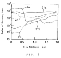
Fig. 2 is a graph showing the distribution of an Ia-group element in the direction of the thickness of a semiconductor thin film having a chalcopyrite structure obtained by the method of the present invention, which is measured by a secondary ion mass spectroscope (SIMS).
-
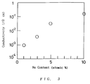
Fig. 3 is a chart showing the change of the conductivity of a CuInSe2:Na film with change in the content of Na.
-
Fig. 4 is a sectional view schematically showing a sputtering device for manufacturing an oxide precursor for the formation of a semiconductor thin film according to the embodiment of the present invention.
-
Fig. 5 is a sectional view showing the structure of the precursor for producing a semiconductor thin film according to the embodiment of the present invention.
-
Fig. 6 is a sectional view showing the structure of a precursor for producing a semiconductor thin film according to another embodiment of the present invention.
-
Fig. 7 is a chart showing the change of the conductivity of a CuInS2 film with respect to the thicknesses of Li2O2 and P2O5 films.
-
Fig. 8 is a sectional view showing the structure of the precursor for producing a semiconductor thin film according to the embodiment of the present invention.
-
Fig. 9 is a chart showing the voltage-current characteristic of the CuInS2 film in which Mg and P are doped.
-
Fig. 10 is a chart showing the X-ray diffraction pattern of the oxide precursor obtained according to an embodiment of the present invention.
-
Fig. 11 is a chart showing the X-ray diffraction pattern of a Cu(In,Ga)Se2 film obtained according to an embodiment of the present invention.
-
Fig. 12 is a graph showing the composition distribution in the direction of the thickness of an oxide precursor film obtained according to one of the embodiments of the present invention.
-
Fig. 13 is a graph showing the composition distribution in the direction of the thickness of the Cu(In,Ga)Se2 film obtained according to one of the embodiments of the present invention.
-
Fig. 14 is a schematically sectional view showing another sputtering device used for the manufacture of an oxide precursor film according to the embodiment of the present invention.
-
Fig. 15 is a sectional view showing the structure of an oxide precursor film obtained according to another embodiment of the present invention.
-
Fig. 16 is a sectional view showing the structure of an oxide precursor film obtained according to still another embodiment of the present invention.
-
Fig. 17 is a graph showing the composition distribution in the direction of the thickness of the oxide precursor film according to one of the embodiments of the present invention.
-
Fig. 18 is a graph showing the composition distribution in the direction of the thickness of the Cu(In,Ga)Se2 film obtained according to one of the embodiments of the present invention.
-
A small amount of a Ia-, Va- or Vb-group element which acts as a p type dopant is added to, or an oxide film which comprises any of these elements is laminated on, an oxide thin film which comprises Ib- and IIIa group elements so that a precursor is formed. Then, the precursor is heat treated in an atmosphere which contains a VIa-group element. Thus, a semiconductor thin film having a chalcopyrite structure which comprises the Ib-, IIIa- and VIa-group elements is produced. At the step where the semiconductor thin film is formed, the element which acts as a dopant is incorporated into the semiconductor thin film. Consequently, it is possible to obtain a film, having very few defects and impurity phases that are different from the semiconductor, as a main product. Thus, doping can be performed on the semiconductor film effectively. It is effective to give the ununiform distribution of a carrier concentration to the semiconductor film in the thickness direction in order to enhance the efficiency of a solar cell. In a pn junction in which an n type semiconductor film is formed on a p type semiconductor film having a chalcopyrite structure where the carrier concentration is increased in the vicinity of a metal that acts as an electrode and gradually decreased toward the film surface, an electric field is generated by the diffusion potential in a depletion layer area on a pn junction portion and an internal electric field is generated in the film due to a difference in carrier concentration. A small number of photo-excited carriers are moved by the internal electric field, collected on a pn junction face and fetched to the outside. The recombination probability is decreased more in an absorber layer by the movement of carriers caused by the electric field than by the movement of carriers caused by diffusion. Consequently, a large amount of photocurrent can be obtained. When the carrier concentration is increased in the vicinity of the pn junction, the diffusion potential becomes larger so that an open circuit voltage is increased. Accordingly, it is apparent that a solar cell having the best efficiency obtained by the combined distribution of two carrier concentrations can be provided. The distribution of the carrier concentration closely corresponds to that of an impurity, i.e., a dopant. By distributing the Ia-group element as an impurity in the thickness direction of the semiconductor thin film having a chalcopyrite structure, the internal electric field can be induced by the carrier concentration distribution. Accordingly, it is apparent that the carrier concentration distribution can be controlled by distributing the Ia-, Va- or Vb-group element which acts as a dopant in the oxide precursor.
-
In the case where the pn homo-junction of the semiconductor thin film having a chalcopyrite structure is formed, a surface or back face (an interface between a thin film and a substrate) which acts as a thin film interface should be changed to have an n type because a CuInSe2 system thin film is a p type semiconductor. Accordingly, if the IIa- or IIb-group element which acts as an n type dopant is added to the surface or the back face, the pn homo-junction can be formed. Furthermore, if the Ia-, Va- or Vb-group element which acts as a p type dopant is combined, it is possible to form a pn junction in which the diffusion potential or depletion layer width is controlled.
-
A precursor for manufacturing a semiconductor thin film and a method for manufacturing a semiconductor thin film according to the present invention wherein the distribution of a forbidden band gap is controlled will be described below.
-
A metallic film that comprises 2 or more IIIa-group elements, i.e., In and Ga is heat treated in the atmosphere which contains the VIa-group element, such as in a gas which contains H2Se. Thus, a Cu(In,Ga)Se2 film is formed. In the Cu(In,Ga)Se2 film, the ununiform distribution of In and Ga sometimes occurs in the direction of a film thickness due to the difference between the diffusion speeds of In and Ga depending on a heat treating temperature. However, heat treating at a high temperature, i.e., 500°C or more is required in order to produce a Cu(In,Ga)Se2 film having excellent crystalline quality in which a high conversion efficiency can be obtained as a solar cell. In this case, In and Ga are mixed uniformly. Accordingly, it is hard to change the forbidden band gap intentionally. On the other hand, even if a two-layered oxide thin film such as a Cu-In-O and Cu-Ga-O film is sintered at a high heat treating temperature, the degree of mutual diffusion of In and Ga is low. Accordingly, if the composition ratio in the thickness direction is set to a desired composition ratio in the oxide thin film of the precursor, the sintered semiconductor thin film having a chalcopyrite structure keeps almost the same distribution of the IIIa-group element as the distribution in the precursor. Consequently, the distribution of the IIIa-group element of the precursor is controlled so that the distribution of the composition ratio of the semiconductor having a chalcopyrite structure can be set to the desired distribution. Thus, the forbidden band gap can be changed.
-
Also in a first embodiment in which the forbidden band gap is controlled according to the present invention, an oxide which comprises the Ib- and IIIa-group elements deposited on a substrate is an oxide thin film which contains the Ib-group element and at least two or more IIIa-group elements. The composition ratio of at least two or more IIIa-group elements is varied in the direction of film thickness, i.e., from the substrate to the deposited oxide thin film surface, so as to be continuously varied. For example, when the oxide thin film is formed in such a manner that the contents of Ga and In which are the IIIa-group elements are decreased and increased respectively, Ga and In of the Cu(In,Ga)Se2 film obtained after heat treatment in the H2Se gas are decreased and increased from the substrate to the film surface respectively, similar to the oxide thin film. In this case, an area which contains more Ga has a larger forbidden band gap. Therefore, the Cu(In,Ga)Se2 film in which the forbidden band gap is gradually narrowed from the substrate to the film surface can be obtained. If a solar cell is fabricated by using the Cu(In,Ga)Se2 film as a semiconductor thin film for an absorber, the carriers that are photo-excited in the vicinity of the electrode comprising a substrate are moved to the pn junction face by the internal electric field generated by the change of the forbidden band gap. Accordingly, the carriers can be taken out to the outside efficiently so that a photocurrent is increased. Also the precursor comprising multiple stacked oxide films which contain specific IIIa-group elements at different composition ratios described in a second embodiment of the present invention allows the change of the forbidden band gap to be implemented.
-
According to the second embodiment of the present invention wherein the forbidden band gap is controlled, oxide thin films, comprising Ib- and IIIa-group elements deposited on a substrate are oxide thin films comprise a Ib-group element and at least one IIIa-group element, and the oxide thin films comprise two or more layers in which the composition ratio of specific IIIa-group elements to all IIIa-group elements is varied, are sequentially deposited so that a stacked oxide thin film is formed with variation of the composition ratio of the specific IIIa-group element. In each layer, the content rate of the Ib-group element and that of the IIIa-group element are the same respectively. However, the content rate of the specific IIIa-group element is changed in every layer. An example will be described below. In the case where a Cu-In0.8-Ga0.2-O film and a Cu-In-O film are stacked as first and second layers, the content rate of the Ib-group element is the same as that of the IIIa-group element in each layer, i.e., the ratio of numbers of atoms is 1 : 1 on each layer. The content rate of In as the specific IIIa-group element is 0.8 on a first layer and 1 on a second layer. As a matter of course, each layer may include two or more kinds of IIIa-group elements. In the case where a Cu-In0.6-Ga0.4-O film and a Cu-In0.8-Ga0.2-O film are combined as first and second layers, the content rate of the Ib-group element is the same as that of the IIIa-group element on each layer, i.e., the ratio of numbers of atoms is 1 : 1 on each layer. The content rate of In as the specific IIIa-group element is 0.6 on a first layer and 0.8 on a second layer. Such a case is included in the second embodiment. Also in such a second embodiment, in the case where a semiconductor thin film having a chalcopyrite structure is produced from the oxide film, the composition ratio of the Ib-group element and the IIIa-group element of each oxide thin film is kept so that the forbidden band gap can be changed by a multi-layered film.
-
According to a third embodiment of the present invention in which a forbidden band gap is controlled, two or more kinds of oxide thin films having different kinds of IIIa-group elements are sequentially deposited to form an oxide thin film having two or more layers, in which the kind of the IIIa-group element is varied as the oxide thin films which comprise the Ib- and IIIa-group elements are deposited on a substrate. In the case where a precursor which is formed by sequentially depositing a Cu-Ga-O film and a Cu-In-O film on an electrode as the substrate is used, the forbidden band gap is rapidly changed in the vicinity of the substrate if a semiconductor thin film having a chalcopyrite structure is produced from the oxide thin film. Consequently, it is hard for photocarriers generated in the vicinity of the electrode to move to the electrode due to an internal electric field caused by the rapid change of the forbidden band gap. Thus, the recombination which occurs through the electrode can be prevented. Accordingly, the carriers can be taken out to the outside efficiently.
-
According to a preferred embodiment of the present invention (of the type in which a forbidden band gap is controlled), the IIIa-group element includes at least Ga in the deposited oxide thin film comprising Ib- and IIIa-group elements that is in contact with the substrate side since a material such as CuGaSe2 or CuGaS2 has better adhesion than CuInSe2 or CuInS2 when a metal body or a metal film is used as a substrate. Accordingly, when a film that contains at least Ga, for example a Cu-Ga-O film or a Cu-In-Ga-O film is deposited on the substrate and sintered, a semiconductor thin film having a chalcopyrite structure which has excellent adhesion to the substrate can be obtained.
-
According to a preferred embodiment in which a substrate is a metal body substrate or an insulator substrate coated with a metal thin film, with a precursor for manufacturing a semiconductor thin film of the present invention in which a forbidden band gap is controlled, the metal body substrate or metal thin film can be used as an electrode when forming a solar cell. The precursor according to the present embodiment can be used for a so-called substrate type solar cell which is used by irradiating light on the semiconductor thin film.
-
By using an oxide thin film deposited on a transparent insulator such as glass that is coated with a transparent conductive film, or on a transparent insulator such as a glass that is coated with the transparent conductive film and a transparent insulator film, a semiconductor thin film having a chalcopyrite structure is formed. The semiconductor thin film can be applied effectively to a superstrate type solar cell which develops electromotive force by irradiating sunlight on the transparent insulator face that is not coated with the transparent conductive film. In this case, a pn junction layer is formed in the vicinity of the substrate surface. Consequently, Ga is gradually increased from the substrate to the semiconductor thin film surface, conversely to the above-mentioned embodiment, so that an internal electric field which moves the photocarriers to the pn junction layer can be generated.
-
According to a method for manufacturing a semiconductor thin film of the present invention (of the forbidden band gap controlled type), a precursor for manufacturing the semiconductor thin film described above is heat treated in an atmosphere containing a VIa-group element so that a semiconductor thin film having a chalcopyrite structure which comprises Ib-, IIIa- and VIa-group elements is formed. As described above, the change of composition (composition distribution) of the IIIa-group element in the direction of the film thickness can be set to a desired composition ratio by using the oxide thin film precursor. Even if the oxide thin film is heat treated in the atmosphere containing the VIa-group element to obtain the semiconductor thin film having a chalcopyrite structure, the degree of interdiffusion of the IIIa-group elements contained in the oxide thin film , for example, the degree of interdiffusion of In and Ga, is small. Accordingly, if the composition ratio for the IIIa-group elements in the direction of film thickness is set to a desired composition ratio in the oxide thin film of the precursor, the distribution of the IIIa-group element is closely maintained in the semiconductor thin film having a chalcopyrite structure after sintering. Consequently, when the distribution of the IIIa-group element of the precursor is controlled, the distribution of the composition ratio of the semiconductor having a chalcopyrite structure can be set to the desired distribution. Thus, the forbidden band gap can be changed in the thickness direction of the semiconductor thin film.
-
In the method for manufacturing a semiconductor thin film according to the present invention described above, it is preferred that heat treatment is performed in the presence of at least one of hydrogen and carbon monoxide. The reaction in which the oxide thin film is heat treated in the atmosphere containing the VIa-group element to produce the semiconductor thin film having a chalcopyrite structure mainly comprises the reducing reaction in which an oxide is reduced. The hydrogen or carbon monoxide has the reduction function so that the conversion of the oxide to the semiconductor thin film can be promoted.
-
In the method for manufacturing a semiconductor thin film according to the present invention described above, it is preferred that heat treatment is performed at a temperature of 200°C to 1000°C. Consequently, the reducing reaction is promoted well at a temperature of 200°C to 1000°C and a product is rarely decomposed.
-
By employing, as an absorber, the semiconductor thin film using the precursor according to the present invention, a solar cell having a high and uniform energy conversion efficiency over a large area and excellent productivity can be provided.
-
Thus, the present invention provides a precursor for manufacturing a semiconductor thin film and a method for manufacturing a semiconductor thin film suitable for a solar cell having high energy conversion efficiency and excellent productivity.
-
Examples of the Ib-group element used for the present invention are Cu and Ag. In particular, Cu is more preferable in terms of cost. Examples of the IIIa-group element are Ga, In and Al. Ga and In are more preferable. Examples of an element which acts as a p type dopant are Li, Na, K, Rb, Cs, Fr and the like. Examples of the Va-group element are N, P, As, Sb and Bi. Examples of the Vb-group element are V, Nb and Ta. In terms of cost, the crystalline quality of the semiconductor thin film having a chalcopyrite structure which has been sintered, safety of handling, and activation as a dopant, Li, Na and K of the Ia-group element, P of the Va-group element, and Nb and Ta of the Vb-group element are more preferable. Examples of an element which acts as an n type dopant are as follows. Examples of the IIa-group element are Be, Mg, Ca, Sr, Ba, Ra and the like. Examples of the IIb-group element are Zn, Cd and Hg. In terms of safety, Mg, Ca, Sr and Ba of the IIa-group element and Zn of the IIb-group element are more preferable. Furthermore, S, Se and Te are used as the VIa-group element. In particular, S and Se are more preferable because they provide a forbidden band gap suitable for the absorption of sunlight.
-
When heat treating the oxide thin film precursor including the Ib- and IIIa-group elements as main component according to the present invention in the atmosphere containing the VIa-group element so as to form the semiconductor thin film having a chalcopyrite structure which comprises the Ib-, IIIa- and VIa-group elements, a substance which contains the VIa-group element can be used, for example, the simple substance of the VIa-group element, a hydride such as H2Se or H2S, a carbide such as CS2, and an organometallic compound such as (CH3)2Se or (C2H5)2Se. In particular, the hydride of the VIa-group element is more preferable.
-
Preferred examples of the present invention will be described with reference to the drawings. The present invention is not restricted to the following examples.
(Example 1)
-
Figs. 1 (a) and (b) are sectional views showing the typical steps of manufacturing a semiconductor thin film having a chalcopyrite structure according to an example of the present invention. As shown in Fig. 1(a), a glass substrate coated with a Mo film is used as a substrate 1. When manufacturing a solar cell, Mo can be preferably used as an ohmic electrode. For this reason, the glass substrate was coated with Mo in advance. Then, a Cu-In-O : Na2O2 film was sputter-deposited, as an oxide thin film precursor 2 comprising Ia-, Ib- and IIIa-group elements, on the Mo film. The Cu-In-O : Na2O2 film means an oxide film of Cu and In containing Na2O2 (Na oxide) as a dopant. Sputter deposition was performed in the Ar atmosphere containing 5 vol% of O2 at a vacuum of 8 x 10⁻³ Torr by the high frequency magnetron sputtering method using, as a target, a sintered body that contains Na2O2 in Cu2In2O5. The thickness of the Cu-In-O : Na2O2 film thus formed is 1.0 µm. Four kinds of oxide precursors having Na contents of about 1 atomic% to 10 atomic% were formed. The substrate coated with the oxide thin film was put in a silica tube and heat treated for 1 hr. at a temperature of 550°C in an atmosphere containing 3 vol% of H2Se which is Ar-diluted and H2 (H2Se + Ar : H2 = 5 : 1 by volume) to form a CuInSe2 : Na thin film as a semiconductor thin film having a chalcopyrite structure comprising Ib-, IIIa- and VIa-group elements (wherein " : Na" means that Na is contained as a dopant).
-
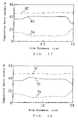
A curve 21a of Fig. 2 shows the result obtained by measuring the Na distribution in the thickness direction of the CuInSe2 : Na thin film having a Na content of 5 atomic% by secondary ion mass spectroscopy (SIMS). An axis of abscissa indicates a film thickness, wherein a film thickness of 0 represents the surface of the formed film. It is apparent that Na is uniformly distributed in the direction of the film thickness.
-
Fig. 3 shows the change of the conductivity of the CuInSe2 : Na thin film with Na content. It is apparent that the conductivity rises as the Na content is increased. If the Na content is less than 5 atomic%, the conductivity rises rectilinearly. When the Na content reaches 10 atomic%, the rising rate is decreased. The reason is that Na contained in the film functions as a dopant effectively with the Na content of 5 atomic% or less to increase a carrier concentration and that the rate at which Na contained in the film functions as the dopant is decreased with the Na content of 10 atomic%. In some cases, a large amount of dopant greatly changes the properties of a semiconductor. It is apparent that the Na content is preferably 5 atomic% or less in the present example.
-
According to the oxide thin film that comprises Ib- and IIIa-group elements and an element which acts as a dopant, the carrier concentration of the semiconductor thin film having a chalcopyrite structure which is finally obtained can be controlled by the amount of the element added as a dopant. In this case, when the element which acts as the dopant is uniformly distributed over the film, the carrier distribution becomes uniform. Such a structure can be formed most easily, and is suitable for mass production.
-
By using a device shown in fig. 4, an oxide precursor in which the amount of Na is distributed in the thickness direction of the film can be formed. A sintered body of Cu2In2O5 : Na2O2 having Na content of 10 atomic% is used as a target 3 shown in Fig. 4, and a sintered body of Cu2In2O5 which does not contain Na is used as a target 4 shown in Fig. 4. These targets are simultaneously sputtered in the Ar atmosphere containing 5 vol% of O2 at a vacuum of 8 x 10⁻³ Torr. The reference numeral 30 designates a gas inlet, and the reference numeral 31 designates a gas outlet. During sputtering, shielding plates 5 and 6 were opened, and particles flying from the sputtered targets were deposited on a substrate 8 during rotation of a substrate holding table 7 in order to obtain a uniform composition across the film surface direction. By adjusting the applied power of high voltage power supplies 10 and 11 of the targets, the speed at which Cu-In-O : Na2O2 and Cu-In-O are deposited can be controlled. Accordingly, the power applied to the targets is changed so that the Cu-In-O : Na2O2 film in which the amount of Na is distributed in the direction of a film thickness can be deposited on the substrate. From the start to the end of film deposition, the power applied to the Cu2In2O5 : Na2O2 target is rectilinearly changed from 1 KW to 100 W and the power applied to the Cu2In2O5 target is rectilinearly changed from 200 W to 1 KW. A curve 21b of Fig. 2 shows the result obtained by measuring the Na distribution of the CuInSe2 : Na thin film, which is reduced by heat treating the Cu-In-O : Na2O2 film under the above conditions, by secondary ion mass spectroscopy (SIMS). It is apparent that the amount of Na is increased from the film surface side to the film substrate side in the direction of a thickness. Accordingly, it is seen that the Na distribution of the precursor is essentially maintained in the semiconductor thin film having a chalcopyrite structure. Thus, the element which acts as the dopant of the precursor is distributed in the thickness direction so that the distribution of a carrier concentration described above can be formed in the direction of the thickness of the semiconductor thin film. Consequently, the efficiency of the solar cell can be enhanced.
-
Na of the Ia-group element was used as the dopant in the present example. Also in the case where P of the Va-group element and Nb and Ta of the Vb-group element were used, the same results were obtained. In particular, when using Nb and Ta, the distribution of the dopant element of the precursor was maintained in the final CuInSe2 film almost completely.
(Example 2)
-
Fig. 5 is a sectional view showing the structure of a precursor formed of an oxide thin film according to an embodiment of the present invention. A stainless steel substrate coated with Mo was used as a
substrate 12. A Cu-In-Ga-O : K
2O
2 film 13 having a K content of 2 atomic%, a Cu-In-Ga-O : K
2O
2 film 14 having a K content of 1 atomic%, and a Cu-In-Ga-O : K
2O
2 film 15 having a K content of 5 atomic% were sequentially deposited on the
substrate 12. Deposition was performed by sputtering under the same conditions as in Example 1. Each film was produced by using a target in which K
2O
2 is contained in Cu
2In
2O
5 in such a manner that the K content has the above ratio. The composition ratio of elements of each film or target is constant, i.e.,
. The substrate coated with the oxide thin film was put in a silica tube and heat treated for 1 hr. at a temperature of 550°C in an atmosphere containing H
2S and H
2 (H
2S : H
2 = 1 : 4 volumeric ratio). Thus, a semiconductor thin film having a chalcopyrite structure which comprises Ib-, IIIa- and VIa-group elements, i.e., a Cu(In, Ga)S
2 : K thin film was formed.
-
In Fig. 2, a curve 22 shows the result obtained by measuring the K distribution in the thickness direction of the Cu(In, Ga)S2 : K thin film by SIMS. Although slight diffusion is caused by heat treatment, the K distribution shown in Fig. 2 almost corresponded to the K distribution obtained when manufacturing the precursor.
-
By depositing an oxide thin film that comprises a plurality of elements that act as dopants with different content ratios and Ib- and IIIa-group elements, the complicated distribution of a carrier concentration in the direction of film thickness described above can be formed comparatively easily and with great precision. Accordingly, the present invention is effective in optionally distributing the elements as dopants in the oxide thin film with great precision.
(Example 3)
-
Fig. 6 is a sectional view showing the structure of a precursor formed of an oxide thin film according to another embodiment of the present invention. A glass substrate coated with a Mo film was used as a substrate 16. An Ia-group oxide thin film 17, i.e. Li2O2 was deposited on the substrate 16. A Cu-In-O film 18, i.e. comprising Ib- and IIIa-group elements, was deposited on the Li2O2 film. The Li2O2 film was produced by high-frequency sputtering a Li2O2 target at 1 KW in an Ar atmosphere containing about 5 vol% of O2 at a vacuum of 8 x 10⁻³ Torr. The Cu-In-O film was produced by the sputtering method in the Ar atmosphere containing 5 vol% of O2 at a vacuum of 8 x 10⁻³ Torr by means of a sintered body of Cu2In2O5 as a target. Five kinds of films were produced, in which the thickness of the Li2O2 film as a first layer is varied within 10 to 100 nm. The thickness of the Cu-In-O film was constant, i.e., 0.8 µm. The obtained oxide precursors were put in a silica tube and heat treated for 1 hr. at a temperature of 550°C in the mixed CS2 and CO atmosphere in which H2 gas was flowed as a carrier gas. Thus, CuInS2 : Li films were produced.
-
In Fig. 2, a curve 23 shows the distribution of Li in the direction of the thickness of the CuInS2 : Li film which was produced by sulfurization of the precursor in the case where the Li2O2 film has a thickness of 50 nm, in which the distribution of Li is gradually increased from the film surface to the substrate side. It is supposed that Li is distributed over the film as shown because it has a small atomic radius or ionic radius for easy diffusion.
-
In Fig. 7, a mark of ○ shows the change of the conductivity of the CuInS2 : Li film with the thickness of the Li2O2 film. It is apparent that the conductivity is increased as the thickness of the Li2O2 film is increased. Consequently, it is seen that the conductivity or carrier concentration of the semiconductor thin film can be controlled easily according to the thickness of the Li2O2 film.
-
The present invention allows for easily controlling an amount of the element as a dopant of the oxide thin film with high precision. An oxide thin film comprising Ib- and IIIa-group elements and an oxide thin film that acts as the dopant are alternately deposited to form a plurality of layers. Thus, the composition ratio of the elements that act as the dopants can be controlled comparatively precisely according to the film thickness ratio. In a structure where a solar cell is formed on a metal body or a metal film, an oxide film comprising an element as a dopant is deposited on the metal body or metal film and an oxide film comprising Ib- and IIIa-group elements is deposited on the oxide film comprising the element as the dopant so that the carrier concentration is increased in the vicinity of the metal body interface or metal film interface. In this case, an electric field is formed in the vicinity of the metal body interface or metal film interface. Consequently, most of the photocarriers that are excited in the vicinity of the metal body interface or metal film interface move to the CuInS2 : Li film surface. Accordingly, the recombination of the carriers can be prevented from occurring at the metal body interface or metal film interface. Thus, it is possible to increase the photocurrent that can be taken out when using the solar cell.
(Example 4)
-
A CuInS2 : P film was manufactured by using an oxide thin film comprising P2O5 as a dopant in place of Li2O2 in the same manufacturing process as in Example 3. In Fig. 6, a glass substrate coated with a Mo film was used as a substrate 16. An oxide thin film 17 comprising Va-group element, i.e., P2O5 film was deposited on the substrate 16. A Cu-In-O film 18 comprising Ib- and IIIa-group elements was deposited on the P2O5 film. The P2O5 film was produced by heating P2O5 powder to about 350°C by vacuum deposition. Cu-In-O was produced by the sputtering method under the same conditions as in Example 3. Five kinds of films were produced, in which the thickness of the P2O5 film on a first layer is varied within 10 to 100 nm. The thickness of the Cu-In-O film was constant, i.e., 0.8 µm. The obtained oxide precursors were put in a silica tube and heat treated for 1 hr. at a temperature of 550°C in the mixed CS2 and CO atmosphere in which H2 gas was flowed as a carrier gas. Thus, CuInS2 : P films were produced.
-
In Fig. 7, a mark of ● shows the change of the conductivity of the CuInS2 : P film with the thickness of the P2O5 film. It is apparent that the conductivity is increased as the thickness of the P2O5 film is increased similarly to the Li2O2 film. As compared with Li2O2, P2O5 has a higher conductivity with the same film thickness. Since it is necessary to compare densities and the like, the argument does not hold easily. However, it is supposed that P2O5 directly functions as the dopant better because of substitution of Se for P. In addition, P2O5 has stability and is not toxic, and thus is advantageous in respect of safety of handling.
-
Also in the case where Nb2O5 and Ta2O5 are used in place of P2O5, the same results can be obtained. However, Nb2O5 and Ta2O5 are inferior to P2O5 in rising rate of the conductivity. It is supposed that Nb and Ta are not substituted for Se but form Nb2Se5 and Ta2Se5 to generate a vacancy of Se, which functions as an acceptor for supplying a hole.
(Example 5)
-
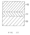
An embodiment that can be applied to a superstrate type solar cell having a structure in which light is incident on a glass face will be described below. A glass substrate was used as a substrate on which a transparent conductive film ZnO: Al2O3 (Al2O3 content of 2 wt%) and a transparent insulating film ZnO were sequentially deposited in thicknesses of 1.5 µm and 0.1 µm. A film comprising Ib- and IIIa-group elements (Cu-In-O) was deposited on the substrate in a thickness of about 1.0 µm by the sputtering deposition method similar to Example 1. A Na2O2 film was deposited on the Cu-In-0 film in a thickness of 50 nm by the sputtering method under the same conditions as in the deposition of the Li2O2 film in Example 3. The obtained oxide precursor was put in a silica tube, and heat treated for 1 hr. at a temperature of 50°C in the atmosphere of H2 gas flow as carrier gas (50 sccm) and (C2H5)2Se vapor flow. Thus, a CuInSe2 : Na film was produced.
-
In Fig. 2, a curve 24 shows the distribution of Na of the thickness direction of the obtained film. Conversely to Example 3, it is apparent that a lot of Na is present on the film surface and is rapidly decreased at about depth of 0.5µm. Na is thermally diffused a little because of a larger atomic radius than that of Li of Example 3. Consequently, the distribution is not extended over the film. Such distribution is also effective in producing a solar cell. In the structure of the solar cell using the film of the present example, a pn junction was formed by n type ZnO and p type CuInSe2, which was located in the vicinity of the substrate. If Na is not doped, carriers which are excited on the film surface far from the glass substrate are not influenced by an electric field generated by the pn junction present in the vicinity of the substrate. Accordingly, the carriers move to the film surface and the substrate side at half probability respectively. An electrode is further formed on the film surface. For this reason, carrier recombination is caused through the electrode so that the carriers are taken out to the outside with difficulties. According to the structure of the present invention, however, a difference in carrier concentration generates the electric field because a carrier concentration is almost equal to the distribution of Na which is a dopant. By the generated electric field, it is hard for the photocarriers excited in the vicinity of the film surface to move to the film surface. Consequently, almost all the photocarriers move to the substrate side. The photocarriers are taken out to the outside through the electric field generated by the pn junction. Accordingly, the photocurrent is increased.
-
The precursor which was formed by laminating an oxide film comprising the Ia-group element and an oxide film comprising the Ib- and IIIa-group elements was used in Examples 3 and 5. According to this structure, the films can be deposited individually so that it is not necessary to sputter two or more targets at the same time. Consequently, the contamination of the targets can be prevented and excellent reproducibility can be obtained. These advantages are effective in the uniform and mass production of a solar cell.
-
While Li2O2, Na2O2 or K2O2 was used as an additive of an oxide film comprising the Ia-group element or an oxide target comprising the Ia-, Ib- and IIIa-group elements in Examples 1 to 3 and 5, the same effects could be obtained even if Li2O, Na2O or K2O is used.
(Example 6)
-
A solar cell was manufactured by using a semiconductor thin film having a chalcopyrite structure produced in Example 1. A film having a Na content of 5 atomic% in Example 1 (a film shown by the curve 21a of Fig. 2) and a film in which the distribution of Na is decreased on the film surface side (a film shown by the curve 21b of Fig. 2) were used. For comparison, a CuInSe2 film was also used. The CuInSe2 film was formed by selenization of a Cu-In-O film which does not contain Na by the same method as in Example 1. A CdS film was deposited as an n type window layer in a thickness of about 50 nm on a CuInSe2 : Na film and the CuInSe2 film for comparison by the solution deposition method using thiourea, cadmium chloride, and aqueous ammonia having a concentration of 1.5 wt%. A ZnO film and a ITO film (In2O3·SnO film having a SnO content of 5 wt%) were deposited as transparent conductive films in thicknesses of 50 nm and 500 nm respectively on the CdS film by the sputtering method. The characteristics of a solar cell using the semiconductor thin film shown by the curve 21a of Fig. 2 had an open circuit voltage Voc of 0.50 V, a short circuit photocurrent Jsc of 40 mA/cm2, a fill factor FF of 0.72, and a conversion efficiency of 15 % under light irradiation of Am1.5, 100 mW/cm2. In case of use of the semiconductor thin film shown by the curve 21b of Fig. 2, a solar cell had Voc of 0.48 V, Jsc of 45 mA/cm2, FF of 0.74 and a conversion efficiency of 16 %. On the other hand, the solar cell characteristics of a film for comparison to which Na is not added had Voc of 0.40 V, Jsc of 42 mA/cm2, FF of 0.68 and a conversion efficiency of 11 %. As described above, it is apparent that the efficiency of the solar cell using the film to which the Ia-group element is added is larger than that of the solar cell using a film for comparison to which the Ia-group element is not added. In particular, the open circuit voltage is high. The reason is that the addition of the Ia-group element increases the carrier concentration of the film and the diffusion potential of the pn junction. According to the solar cell using the semiconductor thin film shown by the curve 21b of Fig. 2 in Example 1 in which the distribution of the Ia-group element of the film is not constant in the direction of the film thickness, the short circuit photocurrent is also larger than that of the solar cell using the film for comparison. The reason is that an internal electric field is generated in the film so that photo-excited carriers are collected efficiently in the pn junction area as described above.
-
The films of Examples 2, 3 and 5 were used to produce the solar cell. As a result, each solar cell had increased in efficiency by 2 to 4% over the solar cell using the film to which the Ia-group element was not added.
-
From the foregoing, it is seen that the efficiency of the solar cell can be enhanced by the addition of the Ia-group element.
(Example 7)
-
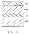
Fig. 8 is a sectional view showing the structure of an oxide thin film precursor according to an embodiment of the present invention. A glass substrate coated with a Mo film was used as a substrate 40. An oxide thin film 41 comprising a Va-group element, i.e. P2O5, was deposited on the substrate 40. A Cu-In-O film 42 comprising Ib- and IIIa-group elements was deposited on the P2O5 film. A MgO film 43 as an oxide thin film comprising a IIa-group element was deposited on the Cu-In-0 film 42. The P2O5 film was formed in a thickness of about 50 nm by the vacuum deposition method under the same conditions as in Example 4. The Cu-In-O film was produced by the sputtering method under the same conditions as in Example 3. The MgO film was produced in the Ar atmosphere containing 10 vol% of O2 at a vacuum of 8 x 10⁻³ Torr by the high frequency magnetron sputtering method in which a MgO sintered body acts as a target. MgO thus produced had a thickness of 50 nm. The obtained oxide precursor was put in a silica tube and heat treated for 1 hr. at a temperature of 550°C in the mixed H2 and H2S atmosphere. Thus, the CuInS2 film in which P and Mg are partially doped was produced.
-
An Au electrode film was formed in a thickness of about 0.2µm on the obtained CuInS2 film by the electron beam deposition method. A voltage was applied to the Mo film to measure the electric characteristics, wherein the Au film acts as a ground. Fig. 9 shows voltage-current characteristics. It is apparent that the rectifying characteristics in which the Mo film side is a p type and the Au electrode side is an n type is shown. Accordingly, it was confirmed that an n type CuInS2 layer in which Mg of the IIa-group element acts as a donor is formed on the CuInS2 film surface and a pn homo-junction is formed.
-
Also in the case where a ZnO film comprising Zn as the IIb-element was used as an oxide thin film containing elements which act as dopants, the same results were obtained.
-
A glass substrate coated with an ITO film was used as the substrate 40. The MgO film, the Cu-In-O film and the P2O5 film were used for the oxide thin films 41, 42 and 43 respectively. Thus, the precursor having the reverse structure to that of the above Examples was formed. The precursor was sulfurized to produce the CuInS2 film in which Mg and P are partially doped. Also in the case where the Au electrode film was formed on the CuInS2 film surface to measure voltage-current characteristics, the same rectifying characteristics were observed. In this case, the CuInS2 layer on the ITO film side was an n type and the CuInS2 layer on the Au film side was a p type.
-
Thus, the oxide thin film comprising the IIa- and IIb-group elements is deposited on the oxide thin film comprising the Ib- and IIIa-group elements and heat treated so that an n type semiconductor thin film having a chalcopyrite structure can be produced easily. Accordingly, it is not necessary to expose the formed p type semiconductor thin film to the air in order to form an n type window layer. Thus, it is possible to prevent the formation of oxide layers and impurity layers on the pn junction interface. Consequently, the center of carrier recombination is not increased and energy barriers are not generated by the oxide layers and the impurity layers. Hence, the conversion efficiency of the solar cell can be enhanced. In addition, the ununiformity of the conversion efficiency owing to generation of the oxide layers and the impurity layers can be prevented. Thus, uniform conversion efficiency can be realized over a large area. Accordingly, the semiconductor thin film solar cell having a pn homo-junction chalcopyrite structure according to the present invention has excellent productivity and is industrially advantageous.
(Example 8)
-
By the following method using the same sputtering device as in Fig. 4, an oxide thin film was deposited. A glass substrate coated with Mo was used as a substrate 8. In the case where a solar cell is produced, Mo is preferably used as an ohmic electrode. For this reason, the glass substrate is coated with Mo in advance. Sintered bodies of Cu-Ga-O and Cu-In-O were used as oxide targets 3 and 4. The mixed gas of Ar and O2 (volumeric ratio Ar : O2 = 95 :5) was introduced from a gas inlet 30. At a vacuum of 8 x 10⁻³ Torr, a high voltage was applied to a substrate holding plate 7 and targets 3 and 4, the gas was ionized and the targets were sputtered. At this time, shielding plates 5 and 6 were opened, and particles which fly from the sputtered targets are deposited on the substrate 8 during rotation of substrate holding plate 7 in order to obtain the uniform composition across the surface of the film. By adjusting the power applied to high voltage supplies 10 and 11 of the targets, the deposition speed of Cu-Ga-O and Cu-In-O could be controlled. Thus, a Cu-In-Ga-O film having an optional composition ratio can be deposited on the substrate according to the power applied to the targets. From the start to the end of film deposition, the power applied to the Cu-Ga-O target was rectilinearly changed from 1KW to 100W and the power applied to the Cu-In-O target was rectilinearly changed from 50W to 1KW. An oxide thin film precursor thus obtained was put in a silica tube and heat treated for 1 hr. at a temperature of 550°C in the atmosphere containing 2 vol% of H2Se diluted with Ar at a vacuum of 500 Torr. Thus, the semiconductor thin film having a chalcopyrite structure which comprises Ib-, IIIa- and VIa-group elements, i.e. a Cu(In, Ga) Se2 thin film, was obtained.
-
Figs. 10 and 11 show the X-ray diffraction patterns of the oxide thin film and the Cu(In, Ga)Se2 thin film respectively. In Fig. 10, it is apparent that a diffraction peak is not observed and the oxide thin film is in the amorphous state. In Fig. 11, it is apparent that a 101 peak peculiar to the chalcopyrite structure is observed and the semiconductor thin film having the chalcopyrite structure has been produced. In the case where the Cu(In, Ga)Se2 film is a mixture of CuInSe2 and CuGaSe2, peak separation is usually observed. However, it is confirmed that the Cu(In, Ga)Se2 film in which In forms a solid solution with Ga has been formed because 112 peak and the like are observed without peak separation.
-
Figs. 12 and 13 show the results obtained by measuring the element distribution of the Cu-In-Ga-O thin film and the Cu(In, Ga)Se2 thin film in the direction of film thickness by Auger electron spectroscopy. An axis of abscissa indicates a film thickness, wherein a thickness of 0 represents the surface of the film. Curves 62 and 72 indicate the distribution of a Cu element. Curves 63 and 73 indicate the distribution of a Ga element. Curves 64 and 74 indicate the distribution of a In element. As is apparent from Fig. 12, Cu of the oxide thin film Cu-In-Ga-O is distributed almost uniformly in the direction of a film thickness, and the distribution of In and Ga is rectilinearly decreased and increased from the film surface to the Mo film side on the substrate respectively. Accordingly, it is seen that the mixing ratios of In and Ga in the film can be controlled by the power applied to the target.
-
As is apparent from Fig. 13, Cu of the Cu(In, Ga)Se2 thin film is uniformly distributed in the direction of a film thickness, and In and Ga of the Cu(In, Ga)Se2 thin film are decreased and increased from the film surface to the Mo film side respectively similarly to the oxide precursor thin film. Accordingly, it is apparent that the Cu(In, Ga)Se2 film maintains the composition distribution of the oxide thin film.
-
A CdS film (n type semiconductor film) was deposited on the Cu(In, Ga)Se2 film (p type semiconductor film) by the solution deposition method using cadmium chloride and thiourea in which aqueous ammonia having a concentration of 1.5 wt% acts as a solvent. An insulating film ZnO and an ITO film (an In2O3 · SnO film having a SnO content of 5 wt%) as a transparent electrode were further deposited by the sputtering method. Thus, a solar cell was produced. Light of AM1.5, 100 mW/cm2 was irradiated on the solar cell to measure current-voltage characteristics. As a result, a conversion efficiency of 12% or more was obtained. This value is higher than that of a solar cell using a Cu(In0.6Ga0.4)Se2 thin film which has the uniform composition (a conversion efficiency of about 10%).
-
Also in the case of using a sputtering device shown in Fig. 14, it is possible to manufacture a precursor in which the distribution of In and Ga is changed in the direction of a film thickness similarly to the present example. In this case, the power applied to the Cu-Ga-O and Cu-In-0 targets 3 and 4 is constant and a substrate holding plate 7' can be moved in the direction shown by the arrow. Consequently, sputtering is performed while moving the substrate 8 so that the distribution of the composition ratio of Ga and In is changed in the direction of a film thickness. More specifically, if the substrate 8 is in the vicinity of the Cu-Ga-O target 2, the Ga content is great. The In content is increased as the substrate 8 is moved above the Cu-In-O target 4. By using this method, oxide thin film precursors can be formed one after another on a large-area substrate. Thus, the mass production of the solar cell can be realized and costs can be reduced.
(Example 9)
-
Fig. 15 is a sectional view showing the structure of a precursor formed of an oxide thin film according to another embodiment of the present invention. A metal substrate comprising stainless steel coated with a Mo film was used as a substrate 50. Mo was employed because it can be preferably used as an ohmic electrode when producing a solar cell as described above. Stainless steel is used as a package material when finishing the solar cell into a package, and serves as the substrate material and the package material.
-
A Cu-In0.8-Ga0.2-O film 51 was first formed in a thickness of about 0.2µm on the substrate 50. Then, a Cu-In-O film 52 was deposited in a thickness of 0.8µm on the Cu-In0.8-Ga0.2-O film 51. In order to form a precursor, a device shown in Fig. 4 was used. The sintered bodies of Cu-In0.8-Ga0.2-O and Cu-In-O were used for targets 3 and 4. 1 KW of-power was applied to the target and only shielding plate 5 was opened for about 10 minutes to deposit the Cu-In0.8-Ga0.2-O film on the substrate 50 until the above film thickness was obtained in the Ar and O2 atmosphere similar to Example 8. Then, the shielding plate 5 was closed and shielding plate 6 was opened for about 40 minutes to deposit the Cu-In-O film until the above film thickness was obtained. The precursor thus produced was put in a silica tube and heat treated for 1 hr. at a temperature of 550°C in the H2S and H2 atmosphere at a vacuum of about 100 Torr (volumeric ratio H2S : H2 = 1 : 3). Thus, a Cu(In, Ga)S2 film was produced. For comparison, two kinds of precursors in which only Cu-In-O was deposited and only Cu-In0.8-Ga0.2-O was deposited in thicknesses of about 1.0µm on the stainless steel coated with Mo were sulfurized under the same conditions. Thus, a CuInS2 film and a Cu(In0.8Ga0.2)S2 film were produced respectively.
-
There are steps of depositing a window layer, a transparent electrode film and the like on a photoabsorptive layer in order to form a solar cell. It is preferred that the photoabsorptive layer which does not peel off the substrate even though these steps are conducted is produced. In order to check adhesion, the obtained film was put in pure water and ultrasonic cleaning was performed for about 5 minutes. As a result, the CuInS2 film was almost peeled off from the Mo but the Cu(In, Ga)S2 film and the Cu(In0.8Ga0.2)S2 film was not peeled off from the Mo. Accordingly, it is apparent that the CuInS2 film to which Ga is added is more preferable for producing the solar cell.
-
A CdS film was deposited on the obtained Cu(In, Ga)S2 film and the Cu(In0.8Ga0.2)S2 film by the solution deposition method described above. Furthermore, a ZnO film which is a transparent insulating film and ITO film which is a transparent conductive film were deposited by the sputtering method. Thus, the solar cell was produced. AM1.5, 100 mW/cm2 of light was irradiated on the solar cell to measure current-voltage characteristics. As a result, the solar cell using, as the photoabsorptive film, the Cu(In, Ga)S2 film having different compositions of In and Ga in the direction of a film thickness has a conversion efficiency of 12% or more. On the other hand, the solar cell using, as the photoabsorptive film, the Cu(In0Ga0.2)S2 film having a uniform composition in the direction of the film thickness had a conversion efficiency of 10%. The Cu(In, Ga)S2 film having a layer whose forbidden band gap is larger in the vicinity of the Mo film as a back electrode has less photocarrier recombination through the back electrode. Consequently, a greater photocurrent can be generated.
-
Similarly to Example 8, the same precursor as in the present example can be produced by a device shown in Fig. 14. In this case, the movement of the substrate is stopped above the Cu-In0.8-Ga0.2-O target 3 and sputter vapor deposition is performed for a predetermined time until a desired film thickness is obtained. Then, the substrate is moved above the Cu-In-O target 4 and the sputter vapor deposition is performed for a predetermined time until a desired thickness is obtained. Thus, the precursor can be formed easily.
-
While stainless steel was used as the substrate in the present example, the same results can be obtained also in the case where a metal body substrate such as a Mo sheet or an Al sheet is used.
(Example 10)
-
A method for manufacturing a semiconductor thin film comprising Ib-, IIIa- and VIa-group elements in which the different oxide thin film from those of the above examples is used for a precursor will be described below. In Fig. 15, an insulator substrate formed by coating an alumina with a Pt film was used as a substrate 50. A Cu-Ga-O film 51 was first formed in a thickness of about 0.05µm on the substrate and then a Cu-In-O film 52 was formed in a thickness of about 1.0µm on the Cu-Ga-O film 51. In order to form a precursor, the device shown in Fig. 4 was used similarly to Example 9. 0.5 KW and 1 KW of power were applied to the targets and only shielding plate 5 was opened for about 10 minutes to deposit a Cu-Ga-O film on the substrate 50 until the above film thickness was obtained in the Ar and O2 atmosphere in similar to Example 8. Then, the shielding plate 5 was closed and shielding plate 6 was opened for about 50 minutes to deposit a Cu-In-O film until the above film thickness was obtained. For comparison, a precursor in which only the Cu-In-O film was deposited in a thickness of about 1.0µm on the same substrate was produced.
-
The precursors having two-layer and one-layer structures thus produced were put in a silica tube and heat treated for 1 hr. at a temperature of 550°C in a mixture gas atmosphere comprising H2S, Ar and H2 (volumeric ratio H2S : Ar : H2 = 1 : 10 : 3) at a vacuum of about 500 Torr. Thus, a Cu(In, Ga)S2 film having a two-layer structure and a CuInS2 film having a one-layer structure were produced.
-
The film thus obtained was put in pure water and ultrasonic cleaning was performed for 5 minutes. The CuInS2 film was almost peeled off from a Pt film but the Cu(In, Ga)S2 film was not peeled off from the Pt film. It is apparent that a Cu-Ga-O film having a thickness of about 0.05µm is merely deposited on a metal electrode so that adhesion is increased.
-
A CdS film was deposited on the obtained Cu(In, Ga)S2 film by the solution deposition method described above. Furthermore, a ZnO film, which is a transparent insulating film, and an ITO film, which is a transparent conductive film, were deposited by the sputtering method. Thus, a solar cell was produced. AM1.5, 100 mW/cm2 of light was irradiated on the solar cell to measure current-voltage characteristics. As a result, the Cu(In, Ga)S2 film solar cell having a two layer structure had a conversion efficiency of 11% or more, which is a little inferior to that of the Cu(In, Ga)S2 film solar cell of Example 9. The reason is as follows. The CuInS2 film grows on the CuGaS2 film having lattice constants that greatly differ, so that the crystalline properties are inferior to those of the film of Example 9 and the capture center of photocarriers is increased. The present example is inferior to Example 9 in conversion efficiency. However, since the oxide target having the simple composition is used, a difference of composition between the target and the obtained oxide film is not caused by sputtering and the oxide film having the desired composition can be deposited. Consequently, the reproducibility of performance is excellent.
(Example 11)
-
An example of the present invention is applied to a superstrate type solar cell wherein light is incident on the light transmitting substrate side such as a glass.
-
Fig. 16 shows the structure of a precursor formed of an oxide thin film according to the present example. A transparent conductive film ZnO · Al2O3 (Al2O3 content of 2 wt%) and a transparent insulating film ZnO were sequentially deposited on a glass to form a substrate 53. A Cu-(In0.6-Ga0.4)-O film 54 was first deposited on the substrate 53. A Cu-(In0.8-Ga0.2)-O film 55 was deposited on the Cu-(In0.6-Ga0.4) film 54. Finally, a Cu-(In0.7-Ga0.3)-O film 56 was deposited. The thicknesses of the oxide films 54, 55 and 56 are 0.1, 0.6 and 0.3µm. In order to produce a precursor, a device that is formed by adding to the device shown in Fig. 4 a target, a high voltage supply and a shielding plate as another sputtering supply was used. Cu-In0.6-Ga0.4-O, Cu-In0.8-Ga0.2-O and Cu-In0.7-Ga0.3-O were used for targets. 0.5 KW, 1 KW and 1 KW of high frequency power were applied to the respective targets so that sputtering was performed in the same atmosphere as in Example 8. The shielding plate was opened and closed so as to obtain the above film thicknesses. The oxide thin film precursor thus produced was put in a silica tube, and heat treated for 1 hr. at a temperature of 550°C in the atmosphere containing 2 vol% of H2Se diluted with Ar and H2 at a vacuum of 500 Torr (volumeric ratio Ar + H2Se : H2 = 10 : 1). Thus, a Cu(In, Ga)Se2 thin film having a different composition ratio of In and Ga in the direction of thickness was formed.
-
Figs. 17 and 18 show the composition distribution of the precursor and the selenized Cu(In, Ga)Se2 film in the thickness direction obtained by Auger electronic spectroscopy. In Figs. 17 and 18, curves 82 and 92 indicate the composition ratio of Cu, curves 83 and 93 indicate the composition ratio of In, and curves 84 and 94 indicate the composition ratio of Ga. It is apparent that the Cu(In, Ga)Se2 film maintains the distribution of Cu, In and Ga of the oxide precursor. Accordingly, it is seen that the composition of a semiconductor thin film having a chalcopyrite structure that is produced by selenization or sulfurization can be controlled by the composition distribution of the oxide precursor. Consequently, it is possible to design the distribution of the forbidden band gap of a solar cell having a high conversion efficiency. For example, when the Ga content is increased, the forbidden band gap of the Cu(In, Ga)Se2 becomes larger. Accordingly, if a layer having the high Ga content is provided on the interface with a window layer ZnO, an increase in open circuit voltage that is dependent on the forbidden band gap of pn junction can be expected.
-
An Au film was deposited as a back electrode in a thickness of about 0.15µm on the Cu(In, Ga)Se2 film so that the solar cell was produced. AM1.5, 100 mW/cm2 was irradiated on the solar cell to measure current-voltage characteristics. As a result, the solar cell thus obtained had a conversion ratio of 11% or more, which is higher than the conversion efficiency, i.e. about 8%, of a superstrate type Cu(In, Ga)Se2 solar cell produced by depositing each component element by the vapor deposition method.
-
The precursor of the present invention can be manufactured by using the device shown in Fig. 14. In this case, if a target as a sputtering source and a high voltage supply for applying power to the target are added, the precursor can be manufactured by the same procedure as Example 9.
-
While ZnO · Al2O3 and ZnO have been used as the transparent conductive film and the transparent insulating film in the present invention, the same results can be obtained also in the case SnO2 or ITO, and Al2O3 or TiO2 are used as the transparent conductive and insulating films respectively.
-
The precursor for a semiconductor thin film according to the present example is used to produce a semiconductor thin film having a chalcopyrite structure comprising Ib-, IIIa- and VIa-group elements. By using the semiconductor thin film for the photoabsorptive layer of the solar cell, a solar cell having a high and almost uniform conversion efficiency over a large area can be obtained.
-
The present invention can provide a precursor for a semiconductor thin film and a method for manufacturing the semiconductor thin film suitable for a solar cell having a high conversion efficiency and excellent productivity.