EP0768388A2 - Method and apparatus for forming amorphous carbon film - Google Patents
Method and apparatus for forming amorphous carbon film Download PDFInfo
- Publication number
- EP0768388A2 EP0768388A2 EP96114340A EP96114340A EP0768388A2 EP 0768388 A2 EP0768388 A2 EP 0768388A2 EP 96114340 A EP96114340 A EP 96114340A EP 96114340 A EP96114340 A EP 96114340A EP 0768388 A2 EP0768388 A2 EP 0768388A2
- Authority
- EP
- European Patent Office
- Prior art keywords
- reaction chamber
- adhesion
- wall
- thin film
- gas
- Prior art date
- Legal status (The legal status is an assumption and is not a legal conclusion. Google has not performed a legal analysis and makes no representation as to the accuracy of the status listed.)
- Granted
Links
Images


Classifications
-
- C—CHEMISTRY; METALLURGY
- C23—COATING METALLIC MATERIAL; COATING MATERIAL WITH METALLIC MATERIAL; CHEMICAL SURFACE TREATMENT; DIFFUSION TREATMENT OF METALLIC MATERIAL; COATING BY VACUUM EVAPORATION, BY SPUTTERING, BY ION IMPLANTATION OR BY CHEMICAL VAPOUR DEPOSITION, IN GENERAL; INHIBITING CORROSION OF METALLIC MATERIAL OR INCRUSTATION IN GENERAL
- C23C—COATING METALLIC MATERIAL; COATING MATERIAL WITH METALLIC MATERIAL; SURFACE TREATMENT OF METALLIC MATERIAL BY DIFFUSION INTO THE SURFACE, BY CHEMICAL CONVERSION OR SUBSTITUTION; COATING BY VACUUM EVAPORATION, BY SPUTTERING, BY ION IMPLANTATION OR BY CHEMICAL VAPOUR DEPOSITION, IN GENERAL
- C23C16/00—Chemical coating by decomposition of gaseous compounds, without leaving reaction products of surface material in the coating, i.e. chemical vapour deposition [CVD] processes
- C23C16/22—Chemical coating by decomposition of gaseous compounds, without leaving reaction products of surface material in the coating, i.e. chemical vapour deposition [CVD] processes characterised by the deposition of inorganic material, other than metallic material
- C23C16/24—Deposition of silicon only
-
- H—ELECTRICITY
- H01—ELECTRIC ELEMENTS
- H01L—SEMICONDUCTOR DEVICES NOT COVERED BY CLASS H10
- H01L21/00—Processes or apparatus adapted for the manufacture or treatment of semiconductor or solid state devices or of parts thereof
- H01L21/02—Manufacture or treatment of semiconductor devices or of parts thereof
- H01L21/02104—Forming layers
- H01L21/02107—Forming insulating materials on a substrate
- H01L21/02109—Forming insulating materials on a substrate characterised by the type of layer, e.g. type of material, porous/non-porous, pre-cursors, mixtures or laminates
- H01L21/02112—Forming insulating materials on a substrate characterised by the type of layer, e.g. type of material, porous/non-porous, pre-cursors, mixtures or laminates characterised by the material of the layer
- H01L21/02115—Forming insulating materials on a substrate characterised by the type of layer, e.g. type of material, porous/non-porous, pre-cursors, mixtures or laminates characterised by the material of the layer the material being carbon, e.g. alpha-C, diamond or hydrogen doped carbon
-
- C—CHEMISTRY; METALLURGY
- C23—COATING METALLIC MATERIAL; COATING MATERIAL WITH METALLIC MATERIAL; CHEMICAL SURFACE TREATMENT; DIFFUSION TREATMENT OF METALLIC MATERIAL; COATING BY VACUUM EVAPORATION, BY SPUTTERING, BY ION IMPLANTATION OR BY CHEMICAL VAPOUR DEPOSITION, IN GENERAL; INHIBITING CORROSION OF METALLIC MATERIAL OR INCRUSTATION IN GENERAL
- C23C—COATING METALLIC MATERIAL; COATING MATERIAL WITH METALLIC MATERIAL; SURFACE TREATMENT OF METALLIC MATERIAL BY DIFFUSION INTO THE SURFACE, BY CHEMICAL CONVERSION OR SUBSTITUTION; COATING BY VACUUM EVAPORATION, BY SPUTTERING, BY ION IMPLANTATION OR BY CHEMICAL VAPOUR DEPOSITION, IN GENERAL
- C23C16/00—Chemical coating by decomposition of gaseous compounds, without leaving reaction products of surface material in the coating, i.e. chemical vapour deposition [CVD] processes
- C23C16/22—Chemical coating by decomposition of gaseous compounds, without leaving reaction products of surface material in the coating, i.e. chemical vapour deposition [CVD] processes characterised by the deposition of inorganic material, other than metallic material
- C23C16/26—Deposition of carbon only
-
- C—CHEMISTRY; METALLURGY
- C23—COATING METALLIC MATERIAL; COATING MATERIAL WITH METALLIC MATERIAL; CHEMICAL SURFACE TREATMENT; DIFFUSION TREATMENT OF METALLIC MATERIAL; COATING BY VACUUM EVAPORATION, BY SPUTTERING, BY ION IMPLANTATION OR BY CHEMICAL VAPOUR DEPOSITION, IN GENERAL; INHIBITING CORROSION OF METALLIC MATERIAL OR INCRUSTATION IN GENERAL
- C23C—COATING METALLIC MATERIAL; COATING MATERIAL WITH METALLIC MATERIAL; SURFACE TREATMENT OF METALLIC MATERIAL BY DIFFUSION INTO THE SURFACE, BY CHEMICAL CONVERSION OR SUBSTITUTION; COATING BY VACUUM EVAPORATION, BY SPUTTERING, BY ION IMPLANTATION OR BY CHEMICAL VAPOUR DEPOSITION, IN GENERAL
- C23C16/00—Chemical coating by decomposition of gaseous compounds, without leaving reaction products of surface material in the coating, i.e. chemical vapour deposition [CVD] processes
- C23C16/44—Chemical coating by decomposition of gaseous compounds, without leaving reaction products of surface material in the coating, i.e. chemical vapour deposition [CVD] processes characterised by the method of coating
- C23C16/4401—Means for minimising impurities, e.g. dust, moisture or residual gas, in the reaction chamber
-
- H—ELECTRICITY
- H01—ELECTRIC ELEMENTS
- H01L—SEMICONDUCTOR DEVICES NOT COVERED BY CLASS H10
- H01L21/00—Processes or apparatus adapted for the manufacture or treatment of semiconductor or solid state devices or of parts thereof
- H01L21/02—Manufacture or treatment of semiconductor devices or of parts thereof
- H01L21/02104—Forming layers
- H01L21/02107—Forming insulating materials on a substrate
- H01L21/02109—Forming insulating materials on a substrate characterised by the type of layer, e.g. type of material, porous/non-porous, pre-cursors, mixtures or laminates
- H01L21/02112—Forming insulating materials on a substrate characterised by the type of layer, e.g. type of material, porous/non-porous, pre-cursors, mixtures or laminates characterised by the material of the layer
- H01L21/02123—Forming insulating materials on a substrate characterised by the type of layer, e.g. type of material, porous/non-porous, pre-cursors, mixtures or laminates characterised by the material of the layer the material containing silicon
-
- H—ELECTRICITY
- H01—ELECTRIC ELEMENTS
- H01L—SEMICONDUCTOR DEVICES NOT COVERED BY CLASS H10
- H01L21/00—Processes or apparatus adapted for the manufacture or treatment of semiconductor or solid state devices or of parts thereof
- H01L21/02—Manufacture or treatment of semiconductor devices or of parts thereof
- H01L21/02104—Forming layers
- H01L21/02107—Forming insulating materials on a substrate
- H01L21/02225—Forming insulating materials on a substrate characterised by the process for the formation of the insulating layer
- H01L21/0226—Forming insulating materials on a substrate characterised by the process for the formation of the insulating layer formation by a deposition process
- H01L21/02263—Forming insulating materials on a substrate characterised by the process for the formation of the insulating layer formation by a deposition process deposition from the gas or vapour phase
- H01L21/02271—Forming insulating materials on a substrate characterised by the process for the formation of the insulating layer formation by a deposition process deposition from the gas or vapour phase deposition by decomposition or reaction of gaseous or vapour phase compounds, i.e. chemical vapour deposition
- H01L21/02274—Forming insulating materials on a substrate characterised by the process for the formation of the insulating layer formation by a deposition process deposition from the gas or vapour phase deposition by decomposition or reaction of gaseous or vapour phase compounds, i.e. chemical vapour deposition in the presence of a plasma [PECVD]
-
- H—ELECTRICITY
- H01—ELECTRIC ELEMENTS
- H01L—SEMICONDUCTOR DEVICES NOT COVERED BY CLASS H10
- H01L21/00—Processes or apparatus adapted for the manufacture or treatment of semiconductor or solid state devices or of parts thereof
- H01L21/02—Manufacture or treatment of semiconductor devices or of parts thereof
- H01L21/04—Manufacture or treatment of semiconductor devices or of parts thereof the devices having at least one potential-jump barrier or surface barrier, e.g. PN junction, depletion layer or carrier concentration layer
- H01L21/18—Manufacture or treatment of semiconductor devices or of parts thereof the devices having at least one potential-jump barrier or surface barrier, e.g. PN junction, depletion layer or carrier concentration layer the devices having semiconductor bodies comprising elements of Group IV of the Periodic System or AIIIBV compounds with or without impurities, e.g. doping materials
- H01L21/30—Treatment of semiconductor bodies using processes or apparatus not provided for in groups H01L21/20 - H01L21/26
- H01L21/31—Treatment of semiconductor bodies using processes or apparatus not provided for in groups H01L21/20 - H01L21/26 to form insulating layers thereon, e.g. for masking or by using photolithographic techniques; After treatment of these layers; Selection of materials for these layers
- H01L21/312—Organic layers, e.g. photoresist
- H01L21/3127—Layers comprising fluoro (hydro)carbon compounds, e.g. polytetrafluoroethylene
-
- Y—GENERAL TAGGING OF NEW TECHNOLOGICAL DEVELOPMENTS; GENERAL TAGGING OF CROSS-SECTIONAL TECHNOLOGIES SPANNING OVER SEVERAL SECTIONS OF THE IPC; TECHNICAL SUBJECTS COVERED BY FORMER USPC CROSS-REFERENCE ART COLLECTIONS [XRACs] AND DIGESTS
- Y10—TECHNICAL SUBJECTS COVERED BY FORMER USPC
- Y10S—TECHNICAL SUBJECTS COVERED BY FORMER USPC CROSS-REFERENCE ART COLLECTIONS [XRACs] AND DIGESTS
- Y10S438/00—Semiconductor device manufacturing: process
- Y10S438/905—Cleaning of reaction chamber
-
- Y—GENERAL TAGGING OF NEW TECHNOLOGICAL DEVELOPMENTS; GENERAL TAGGING OF CROSS-SECTIONAL TECHNOLOGIES SPANNING OVER SEVERAL SECTIONS OF THE IPC; TECHNICAL SUBJECTS COVERED BY FORMER USPC CROSS-REFERENCE ART COLLECTIONS [XRACs] AND DIGESTS
- Y10—TECHNICAL SUBJECTS COVERED BY FORMER USPC
- Y10S—TECHNICAL SUBJECTS COVERED BY FORMER USPC CROSS-REFERENCE ART COLLECTIONS [XRACs] AND DIGESTS
- Y10S438/00—Semiconductor device manufacturing: process
- Y10S438/931—Silicon carbide semiconductor
Definitions
- the present invention relates to a method and apparatus for forming a thin film by a plasma enhanced chemical vapor deposition method (plasma CVD method), and more particularly to a method and apparatus for forming a thin film, in which an amorphous carbon thin film is formed while preventing deposition of adhesion on the inner wall of a reaction chamber can be prevented.
- plasma CVD method plasma enhanced chemical vapor deposition method
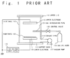
- FIG. 1 is a cross sectional view showing the structure of a conventional parallel plates type plasma enhanced chemical vapor deposition apparatus which is used to form the amorphism carbon film.
- a reaction chamber is composed of a support base 111, a cylindrical side wall 112 which is arranged on the support base 111, and an upper lid 113 provided to oppose to the support base 111 and to close the other end of the cylindrical side wall 112.
- An exhaust pipe 118 is attached to the side wall 112 to be connected to a vacuum pump 117.
- a gas introducing pipe 121 for introducing a material gas into the reaction chamber penetrates the side wall 112.
- the gas introducing pipe 121 has an opening in the reaction chamber at one end and the other end is connected via a control valve 120 to a gas cylinder 119 as a gas supply source.
- a lower plate electrode 114 and an upper plate electrode 115 are arranged in parallel to each other and to oppose to each other in the reaction chamber.
- a substrate 122 for the amorphous carbon film to be formed is mounted on the lower electrode 114.
- the upper electrode 115 is grounded and a predetermined voltage is applied to the lower electrode 114 by a high voltage power supply 116.
- the pressure in the reaction chamber is reduced to a predetermined value by the vacuum pump 117.
- a material gas is supplied from the gas cylinder 119 into the reaction chamber through the gas introducing pipe 121.
- high frequency electric power is applied between the upper electrode 115 and the lower electrode 114 from the high voltage power supply 116 so that high frequency plasma discharge can be generated.
- the material gas there is used a gas which contains, for example, a hydrocarbon gas or a carbon fluoride gas as mainly component.
- the side wall 112 is kept at a temperature equal to about room temperature. As a result, adhesion is deposited on the inner wall of the reaction chamber.
- This adhesion acts as a generation source of an impurity gas when a semiconductor thin film is manufactured. Also, if the adhesion is peeled down from the inner wall of the reaction chamber onto the semiconductor substrate during forming of the thin film, defects are caused a pattern to be formed on the substrate, resulting in decreasing in the manufacturing yield. Further, the film quality of the thin film formed changes, because the state of the plasma to be generated differs between the case that there is not adhesion on the inner wall of the reaction chamber and the case that there is the adhesion on the inner wall, so that active particles differ.
- the deposition of the adhesion of this type and the generation of particles derived from the adhesion have been a general problem in the chemical vapor deposition method.
- the problem has been avoided by mechanically wiping the inner wall of the reaction chamber using organic solvent and so on to remove the adhesion.
- the inner wall of the reaction chamber is made to be detachable and the inner wall is replaced when the semiconductor substrates of a predetermined number is processed.
- etching plasma is generated in the reaction chamber so that the adhesion on the inner wall is removed.
- thermochemical vapor deposition apparatus in which the first reaction gas (e.g., tetraethoxysilane gas) and ozonic (O 3 ) gas are introduced to form a thin film of SiO 2 , deposition of adhesion is reduced by introducing a second reaction gas (e.g., ethylene gas) reacting with oxygen radicals and by heating the wall of the reaction chamber.
- first reaction gas e.g., tetraethoxysilane gas
- ozonic (O 3 ) gas e.g., ozonic (O 3 ) gas
- thermochemical vapor deposition apparatus In the Japanese Laid Open Patent Disclosure (Heisei 5-211125) is disclosed the technique in which in a thermochemical vapor deposition apparatus, the inner wall of a reaction chamber is heated to 50 to 200 °C such that the adhesion deposited on the inner wall of the reaction chamber is sublimated and removed in vacuum.
- thermochemical vapor deposition apparatus in which a compound semiconductor thin film of GaAs or the like is formed using a reaction pipe having the double pipe structure to circulate cooling water, the reaction pipe is divided in three portions along the direction in which a reaction gas flows such that there can be removed the adhesion deposited on the inner wall of the middle one of the three divided portions of the reaction pipe by flowing cooling water through both of end portions of the reaction pile and by heading the middle portion.
- the plasma enhanced chemical vapor deposition apparatus it is required to regularly remove the adhesion deposited on the inner wall of the reaction chamber. For this purpose, the apparatus must be maintained for every predetermined time period. Further, the method is performed in which the conditions of temperature and reaction gas are changed such that the deposition of unnecessary adhesion can be reduced. In the above methods, however, the conditions must be set in accordance with a kind of film to be formed and so on. The condition when an amorphous carbon thin film is formed by the plasma enhanced chemical vapor deposition method does not yet become clear.
- An object of the present invention is to solve the above-mentioned problems and to provide a method for forming a thin film such as an amorphous carbon thin film by the plasma enhanced chemical vapor deposition method while the deposition of adhesion to the inner wall of a reaction chamber can be prevented so that maintenance is not required.
- a method of forming a thin film with a plasma chemical vapor deposition method includes the steps of:
- the reaction chamber is made from a material having a thermal conductivity sufficient to unify a temperature of the whole of the reaction chamber, e.g., aluminum.
- a bias voltage may be applied to the electrically conductive reaction chamber such that the deposition of the adhesion to the inner wall of the reaction chamber is prevented.
- the applied bias voltage is one of DC bias, a high frequency bias and a high frequency bias imposed on a DC bias.
- the material gas includes at least one of hydrocarbon gas or a carbon fluoride.
- the amorphous carbon thin film further includes at least one element selected from the group consisting of hydrogen, fluorine, nitrogen and silicon.
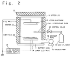
- Fig. 2 is a cross sectional view which shows the structure of a plasma enhanced chemical vapor deposition apparatus according to the first embodiment of the present invention. This chemical vapor-phase growth equipment is used to form an amorphous carbon thin film on a substrate 22.
- a reaction chamber is composed of a support base 11, a cylindrical side wall 12 which is arranged on the support base 11, and an upper lid 13 provided to oppose to the support base 11 and to close the other end of the cylindrical side wall 12.
- An exhaust pipe 18 is attached to the side wall 12 to be connected to a vacuum pump 17.
- a gas introducing pipe 21 for introducing a material gas into the reaction chamber penetrates the side wall 12.
- the gas introducing pipe 21 has an opening in the reaction chamber at one end and the other end is connected via a control valve 20 to a gas cylinder 19 as a gas supply source.
- a lower plate electrode 14 and an upper plate electrode 15 are arranged in parallel to each other and to oppose to each other in the reaction chamber.
- a substrate 22 for the amorphous carbon film to be formed is mounted on the lower electrode 14.
- the upper electrode 15 is grounded and a predetermined voltage is applied to the lower electrode 14 by a high voltage power supply 16.
- the reaction chamber further includes a heater 23 is added around the side wall 12 and on the upper lid 13 such that the heater 23 covers the outside of the reaction chamber, i.e., covers these side walls 12 and the upper lid 13.
- the heater 23 is used to heat the wall of a reaction chamber, especially the inner surface of a side wall 12 and an upper lid 13 where deposition of adhesion becomes the problem, to a predetermined temperature, for example, a temperature equal to or higher than 200 °C.
- a material gas a hydrocarbon gas of CH 4 is used for example.
- a carbon fluoride gas of CF 4 and so on is used as the material gas.
- the hydrocarbon gas and carbon fluoride gas may be properly mixed. If the amorphous carbon thin film which contains nitrogen or silicon is to be formed, a N 2 gas or a silane group gas such as SiH 4 and Si 2 H 6 and so on should be added to these material gases. Then, the inside of the reaction chamber is decompressed by the vacuum pump 18 via the exhaust pipe 18.
- the material gas is introduced from the gas cylinder 19 into the reaction chamber via the control valve 20.
- the inner wall of the reaction chamber is heated to a temperature equal to or higher than 200 °C by the heater 23.
- High frequency electric power is applied between a lower electrode 14 and an upper electrode 15 by the high voltage power supply 16 so that plasma discharge is generated.
- an amorphous carbon thin film is formed on the substrate 22 mounted on lower electrode 14 while preventing any adhesion from depositing on the inner wall of the reaction chamber.
- the thin film such as the amorphous carbon thin film can be grown with good quality and high growth rate.
- the high frequency discharge is used as a plasma generating source.
- the plasma generating source direct current discharge, microwave discharge, helicon wave discharge can be also used.
- the present invention can be applied to the case to use these plasma sources.
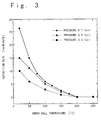
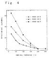
- Figs. 3 and 4 show the measuring results of the temperature dependency of the film deposition rate to the side wall of the reaction chamber when the methane (CH 4 ) is used as the material gas and an amorphous carbon thin film is formed by the parallel plate type plasma chemical vapor deposition apparatus.
- Fig. 3 shows the experimental results when the electric power (source electric power) for the plasma generation is fixed on 200 W and the internal pressure of the reaction chamber is 0.1, 0.2, 0.3 Torr, respectively.
- Fig. 4 shows the experimental results when the internal pressure of the reaction chamber is fixed on 0.1 Torr and the source electric power is set to 100, 200, 300 W, respectively. From these experiment results, it is found that the deposition rate decreases as the temperature of the side wall increases and the adhesion probability of the thin film (adhesion) to the side wall becomes 0 when the temperature of the side wall reaches 200 °C.
- the adhesion probability to the substrate and so on of the film formation active particles which are activated by the plasma has great temperature dependency and the adhesion probability to the inner wall of the reaction chamber is made to be substantially 0 at about 200 °C.
- the temperature that the adhesion to the side wall becomes 0 is constant at 200° C without undergoing the influence of the high frequency electric power (the source electric power) or the pressure. From these results, it could be considered that even if the source electric power and pressure are changed so that the kind and density and so on of the active particles in the plasma are changed, the adhesion coefficient of any of those active particles would become 0 at 200 °C.
- the temperature dependency of adhesion to the inner wall was established in the same manner as mentioned above. That is, in either case of using a hydrocarbon gas such as C 2 H 6 , C 2 H 4 , C 2 H 2 , or C 6 H 6 and a carbon fluoride gas such as CF 4 , C 2 F 6 , or C 4 F 6 as the material gas, the adhesion probability of a film to the inner wall became 0 when the wall temperature became 200 °C. Also, when the whole wall of the reaction chamber was heated to 200 °C and an amorphous carbon thin film was formed using these material gases, adhesion to the inner wall of the reaction chamber could be prevented.
- a hydrocarbon gas such as C 2 H 6 , C 2 H 4 , C 2 H 2 , or C 6 H 6
- a carbon fluoride gas such as CF 4 , C 2 F 6 , or C 4 F 6
- the material which constitutes the reaction chamber will be described.
- the reaction chamber of the chemical vapor deposition apparatus shown in Fig. 2 is made of stainless steel, because a thermal conductivity of stainless steel is small and heat conduction from the heater 23 is different in place, so that a part of the inner wall of the reaction chamber cannot be raised to 200 °C, the deposition of adhesion one is seen only about the part.
- the heating temperature of the reaction chamber is set to 250 °C such that the whole inner wall of the reaction chamber is heated to a temperature equal to or higher than 200 °C, even if a temperature decreased part is formed on the inner wall of the reaction chamber due to the change of thermal conduction in place.
- the film deposition to the inner wall of the reaction chamber can be totally suppressed.
- the reaction chamber is made from aluminum which has a great thermal conductivity and is heated to 200 °C by the heater 23. As a result, the whole reaction chamber is uniformly heated to 200 °C. In this state, an amorphous carbon thin film is formed. As a result, the film deposition to the inner wall of the reaction chamber is not seen. In this manner, if the reaction chamber is made from metal with a great thermal conductivity, the deposition of adhesion to the inner wall of the reaction chamber can be totally prevented at a temperature lower than in a case where the reaction chamber is made from stainless steel.
- Fig. 5 is a cross sectional view which shows the structure of the plasma chemical vapor deposition apparatus according to the second embodiment of the present invention.
- This chemical vapor deposition apparatus is used to form an amorphous carbon thin film on a substrate 22.
- the heater 23 is removed from the plasma chemical vapor deposition apparatus shown in Fig. 2.
- the reaction chamber is made from electrically conductive metal such as stainless steel and aluminum in the second embodiment.
- the plasma chemical vapor deposition apparatus according to the second embodiment is constituted in such a manner that a bias voltage can be applied to the reaction chamber by a high voltage power supply 24.
- the bias voltage is DC voltage or high frequency voltage.
- a shield member 25 which is constituted of metallic network and so on to surround the whole reaction chamber and is grounded.
- a material gas is used a hydrocarbon gas such as CH 4 and so on or a carbon fluoride gas such as CF 4 and so when the film containing fluorine is to be formed.
- the hydrocarbon gas and the carbon fluoride may be properly mixed.
- a N 2 gas or a silane group gas such as SiH 4 and Si 2 H 6 and so on should be added to these material gases.
- the inside of the reaction chamber is decompressed by the vacuum pump 17 via the exhaust pipe 18.
- the material gas is introduced from the gas cylinder 19 into the reaction chamber via the control valve 20.
- High frequency electric power is applied between the lower electrode 14 and the upper electrode 15 by the high voltage power supply 16 such that plasma discharge occurs. Further, a bias voltage of direct current or high frequency is applied to the whole reaction chamber by the high voltage power supply 24, so that the amorphous carbon thin film is formed on the substrate 22 mounted on the lower electrode 14 without depositing any adhesion to the inner wall of the reaction chamber. In this example, the high frequency electric power is applied between the lower electrode 14 and the upper electrode 15 such that the plasma is generated in the reaction chamber.
- direct current discharge, microwave discharge, helicon wave discharge as a plasma generation source. The present invention can be also applied to cases using these plasma sources.
- Fig. 6 shows the adhesion rate of the amorphous carbon film to the inner wall of the reaction chamber when dc or ac bias voltage is applied to the reaction chamber using the above-mentioned chemical vapor deposition apparatus.
- the amorphous carbon thin film is formed using a hydrocarbon gas such as C 2 H 6 , C 2 H 4 , C 2 H 2 , or C 6 H 6 or a carbon fluoride gas such as CF 4 , C 2 F 6 , or C 4 F 8 as the material gas, it is found that the adhesion of the film to the inner wall of the reaction chamber can be prevented when the dc electric power or the high frequency electric power outputted from the high voltage power supply 24 is controlled such that the bias voltage equal to or less than -100 V can be applied to the reaction chamber.
- a hydrocarbon gas such as C 2 H 6 , C 2 H 4 , C 2 H 2 , or C 6 H 6
- a carbon fluoride gas such as CF 4 , C 2 F 6 , or C 4 F 8
- the dc or high frequency bias electric power is to the inner wall of the reaction chamber in a case of formation of the film, ion particles which is generated by the plasma are accelerated and irradiated to the inner wall of the reaction chamber so that etching and sputtering to the film which is adhered to the inner wall would be performed, resulting in prevention of adhesion of the film to the inner wall.
- the bias voltage equal to or less than -100 V is applied to the reaction chamber.
- ions accelerated by the bias voltage equal to or less than -100 V (being equal to or more higher 100 V at the absolute value) to have a high energy contribute to the reduction of the adhesion coefficient to "0". It is shown for the ions to be generated in the same method even if any source electric power is used.
- the adhesion of the film to the inner wall of the reaction chamber could be prevented in the same manner as described above by applying the bias voltage equal to or less than -100 V to the reaction chamber.
- the same result could be obtained in a case where a N 2 gas, or a gas of SiH 4 and Si 2 H 6 were added to the material gas to from the amorphous carbon thin film which contains nitrogen or silicon.
- the particle generation can be prevented without cleaning the inside of the reaction chamber every predetermined constant time period. Also, although a part of the active particles is conventionally deposited on the side wall, because all the active particles are deposited only on the substrate, the film formation rate on the substrate can be increased about twice.
- the reaction product when an amorphous carbon thin film is formed using the plasma enhanced chemical vapor deposition method, the reaction product can be prevented from adhering to the inner wall of the reaction chamber by heating the reaction chamber to a temperature or above at which the adhesion coefficient of the film formation active particle to the inner wall of the reaction chamber becomes 0, or by applying the direct current or high frequency bias voltage to the reaction chamber. In this manner, there is achieved the advantage that it is not necessary to perform regular removal of the adhesion from the reaction chamber , i.e., the effect to make maintenance free.
Abstract
Description
- The present invention relates to a method and apparatus for forming a thin film by a plasma enhanced chemical vapor deposition method (plasma CVD method), and more particularly to a method and apparatus for forming a thin film, in which an amorphous carbon thin film is formed while preventing deposition of adhesion on the inner wall of a reaction chamber can be prevented.
- In manufacturing of a semiconductor device, an amorphous carbon thin film is used as a low dielectric constant insulation material and so on and is formed by the plasma chemical vapor deposition method for example. Fig. 1 is a cross sectional view showing the structure of a conventional parallel plates type plasma enhanced chemical vapor deposition apparatus which is used to form the amorphism carbon film.
- Referring to Fig. 1, in the chemical vapor deposition apparatus, a reaction chamber is composed of a
support base 111, acylindrical side wall 112 which is arranged on thesupport base 111, and anupper lid 113 provided to oppose to thesupport base 111 and to close the other end of thecylindrical side wall 112. An exhaust pipe 118 is attached to theside wall 112 to be connected to avacuum pump 117. Agas introducing pipe 121 for introducing a material gas into the reaction chamber penetrates theside wall 112. Thegas introducing pipe 121 has an opening in the reaction chamber at one end and the other end is connected via acontrol valve 120 to agas cylinder 119 as a gas supply source. Alower plate electrode 114 and anupper plate electrode 115 are arranged in parallel to each other and to oppose to each other in the reaction chamber. Asubstrate 122 for the amorphous carbon film to be formed is mounted on thelower electrode 114. Theupper electrode 115 is grounded and a predetermined voltage is applied to thelower electrode 114 by a highvoltage power supply 116. - When an amorphous carbon thin film is formed using the plasma enhanced chemical vapor deposition apparatus, the pressure in the reaction chamber is reduced to a predetermined value by the
vacuum pump 117. At the same time, a material gas is supplied from thegas cylinder 119 into the reaction chamber through thegas introducing pipe 121. Then, high frequency electric power is applied between theupper electrode 115 and thelower electrode 114 from the highvoltage power supply 116 so that high frequency plasma discharge can be generated. As the material gas, there is used a gas which contains, for example, a hydrocarbon gas or a carbon fluoride gas as mainly component. At this time, theside wall 112 is kept at a temperature equal to about room temperature. As a result, adhesion is deposited on the inner wall of the reaction chamber. - This adhesion acts as a generation source of an impurity gas when a semiconductor thin film is manufactured. Also, if the adhesion is peeled down from the inner wall of the reaction chamber onto the semiconductor substrate during forming of the thin film, defects are caused a pattern to be formed on the substrate, resulting in decreasing in the manufacturing yield. Further, the film quality of the thin film formed changes, because the state of the plasma to be generated differs between the case that there is not adhesion on the inner wall of the reaction chamber and the case that there is the adhesion on the inner wall, so that active particles differ.
- Actually, the deposition of the adhesion of this type and the generation of particles derived from the adhesion have been a general problem in the chemical vapor deposition method. Conventionally, the problem has been avoided by mechanically wiping the inner wall of the reaction chamber using organic solvent and so on to remove the adhesion. Alternatively, the inner wall of the reaction chamber is made to be detachable and the inner wall is replaced when the semiconductor substrates of a predetermined number is processed. Further, there has been used a method in which etching plasma is generated in the reaction chamber so that the adhesion on the inner wall is removed.
- For example, there is disclosed in the Japanese Laid Open Patent Disclosure (Heisei 3-82020) the technique in which a ring member is provided in a reaction chamber of a thermochemical vapor deposition apparatus and an inner wall of the reaction chamber is heated such that the ring member is maintained at a temperature lower than that of the inner wall, so that a fine particle reaction product is made to be adhered to the ring member by thermal migration, resulting in suppression of deposition of the adhesion to the other part of the inner wall.
- In the Japanese Laid Open Patent Disclosure (Heisei 3-183128) is disclosed the technique in which an electrode for removing adhesion and a movable separating member are provided in a reaction chamber of the plasma chemical vapor deposition apparatus and adhesion deposited on the separating member is removed by plasma cleaning using the electrode for removing the adhesion.
- In Japanese Laid Open Patent Disclosure (Heisei 3-211279) is disclosed the technique in which in an atmospheric chemical vapor deposition apparatus in which silane gas and oxygen gas are introduced to form a SiO2 thin film, an exhaust duct and gas dispersion head are heated to 200 °C to 300 °C so that deposition of adhesion (powder of SiO2) to these exhaust duct and gas dispersion head is reduced.
- In Japanese Laid Open Patent Disclosure (Heisei 4-152515) is disclosed the technique in which in a decompression chemical vapor deposition apparatus which is constituted such that a reaction pipe is heated to a temperature as high as a thin film formation temperature, unevenness from 10 µm to 500 µm is provided in the inner wall of the reaction pipe so that a film deposited on the inner wall of the reaction pipe can be prevented from peeling.
- In Japanese Laid Open Patent Disclosure (Heisei 4-186615) is disclosed the technique in which a third electrode is provided in a reaction chamber in a plasma chemical vapor deposition apparatus and plasma etching is performed using the third electrode so that adhesion is removed from the inner wall of the reaction chamber.
- In Japanese Laid Open Patent Disclosure (Heisei 4-262530) is disclosed the technique in which in a thermochemical vapor deposition apparatus in which the first reaction gas (e.g., tetraethoxysilane gas) and ozonic (O3) gas are introduced to form a thin film of SiO2, deposition of adhesion is reduced by introducing a second reaction gas (e.g., ethylene gas) reacting with oxygen radicals and by heating the wall of the reaction chamber.
- In the Japanese Laid Open Patent Disclosure (Heisei 5-211125) is disclosed the technique in which in a thermochemical vapor deposition apparatus, the inner wall of a reaction chamber is heated to 50 to 200 °C such that the adhesion deposited on the inner wall of the reaction chamber is sublimated and removed in vacuum.
- Further, in Japanese Laid Open Patent Disclosure (Heisei 5-217910) is disclosed the technique in which in a thermochemical vapor deposition apparatus in which a compound semiconductor thin film of GaAs or the like is formed using a reaction pipe having the double pipe structure to circulate cooling water, the reaction pipe is divided in three portions along the direction in which a reaction gas flows such that there can be removed the adhesion deposited on the inner wall of the middle one of the three divided portions of the reaction pipe by flowing cooling water through both of end portions of the reaction pile and by heading the middle portion.
- As mentioned above, in the plasma enhanced chemical vapor deposition apparatus, it is required to regularly remove the adhesion deposited on the inner wall of the reaction chamber.
For this purpose, the apparatus must be maintained for every predetermined time period. Further, the method is performed in which the conditions of temperature and reaction gas are changed such that the deposition of unnecessary adhesion can be reduced. In the above methods, however, the conditions must be set in accordance with a kind of film to be formed and so on. The condition when an amorphous carbon thin film is formed by the plasma enhanced chemical vapor deposition method does not yet become clear. - An object of the present invention is to solve the above-mentioned problems and to provide a method for forming a thin film such as an amorphous carbon thin film by the plasma enhanced chemical vapor deposition method while the deposition of adhesion to the inner wall of a reaction chamber can be prevented so that maintenance is not required.
- In order to achieve an aspect of the present invention, a method of forming a thin film with a plasma chemical vapor deposition method, includes the steps of:
- supplying a material gas into a reaction chamber;
- generating a plasma in the reaction chamber using the supplied material gas; and
- depositing an amorphous carbon thin film on a substrate while preventing deposition of an adhesion on an inner wall of the reaction chamber.
- In this case, at least a part of the inner wall of the reaction chamber is heated to a temperature equal to or higher than 200 °C such that adhesion coefficient of the adhesion is 0 so that the deposition of the adhesion on the inner wall of the reaction chamber is prevented. It is desirable that the reaction chamber is made from a material having a thermal conductivity sufficient to unify a temperature of the whole of the reaction chamber, e.g., aluminum. Alternatively, a bias voltage may be applied to the electrically conductive reaction chamber such that the deposition of the adhesion to the inner wall of the reaction chamber is prevented. In this case, the applied bias voltage is one of DC bias, a high frequency bias and a high frequency bias imposed on a DC bias.
- In a case where an amorphous carbon thin film is formed, the material gas includes at least one of hydrocarbon gas or a carbon fluoride. Also, the amorphous carbon thin film further includes at least one element selected from the group consisting of hydrogen, fluorine, nitrogen and silicon.
-
- Fig. 1 is a schematic diagram illustrating the structure of a conventional parallel plate type plasma enhanced chemical vapor deposition apparatus which is used to form an amorphous carbon thin film;
- Fig. 2 is a schematic diagram illustrating the structure of a parallel plate type plasma chemical vapor deposition apparatus according to a first embodiment of the present invention;
- Fig. 3 is a graph showing the temperature dependency of deposition rate of adhesion to a side wall of a reaction chamber when the pressure in the reaction chamber is varied;
- Fig. 4 is a graph showing the temperature dependency of deposition rate of adhesion to the side wall of the reaction chamber when power used to generate plasma is varied;
- Fig. 5 is a schematic diagram illustrating the structure of the parallel plate type plasma chemical vapor deposition apparatus according to a second embodiment of the present invention; and
- Fig. 6 is a graph showing the bias voltage dependency of deposition rate of adhesion to the side wall of the reaction chamber when power used to generate plasma is varied.
- Next, an apparatus for forming a thin film such as an amorphous carbon thin film using a plasma chemical vapor deposition method of the present invention will be described with reference to the drawings.
- Fig. 2 is a cross sectional view which shows the structure of a plasma enhanced chemical vapor deposition apparatus according to the first embodiment of the present invention. This chemical vapor-phase growth equipment is used to form an amorphous carbon thin film on a
substrate 22. - Referring to Fig. 1, in the chemical vapor deposition apparatus, a reaction chamber is composed of a
support base 11, acylindrical side wall 12 which is arranged on thesupport base 11, and anupper lid 13 provided to oppose to thesupport base 11 and to close the other end of thecylindrical side wall 12. An exhaust pipe 18 is attached to theside wall 12 to be connected to avacuum pump 17. Agas introducing pipe 21 for introducing a material gas into the reaction chamber penetrates theside wall 12. Thegas introducing pipe 21 has an opening in the reaction chamber at one end and the other end is connected via acontrol valve 20 to agas cylinder 19 as a gas supply source. Alower plate electrode 14 and anupper plate electrode 15 are arranged in parallel to each other and to oppose to each other in the reaction chamber. Asubstrate 22 for the amorphous carbon film to be formed is mounted on thelower electrode 14. Theupper electrode 15 is grounded and a predetermined voltage is applied to thelower electrode 14 by a highvoltage power supply 16. The reaction chamber further includes aheater 23 is added around theside wall 12 and on theupper lid 13 such that theheater 23 covers the outside of the reaction chamber, i.e., covers theseside walls 12 and theupper lid 13. Theheater 23 is used to heat the wall of a reaction chamber, especially the inner surface of aside wall 12 and anupper lid 13 where deposition of adhesion becomes the problem, to a predetermined temperature, for example, a temperature equal to or higher than 200 °C. - Next, the film formation of the amorphous carbon thin film using this chemical vapor-phase growth equipment will be described. As a material gas, a hydrocarbon gas of CH4 is used for example. When a film containing fluorine is to be deposited, a carbon fluoride gas of CF4 and so on is used as the material gas. The hydrocarbon gas and carbon fluoride gas may be properly mixed. If the amorphous carbon thin film which contains nitrogen or silicon is to be formed, a N2 gas or a silane group gas such as SiH4 and Si2H6 and so on should be added to these material gases. Then, the inside of the reaction chamber is decompressed by the vacuum pump 18 via the exhaust pipe 18. The material gas is introduced from the
gas cylinder 19 into the reaction chamber via thecontrol valve 20. The inner wall of the reaction chamber is heated to a temperature equal to or higher than 200 °C by theheater 23. High frequency electric power is applied between alower electrode 14 and anupper electrode 15 by the highvoltage power supply 16 so that plasma discharge is generated. Thereby, an amorphous carbon thin film is formed on thesubstrate 22 mounted onlower electrode 14 while preventing any adhesion from depositing on the inner wall of the reaction chamber. In this case, because any adhesion is not deposited on the inner wall of the reaction chamber and active particles generated by the plasma discharge can be effectively used for the deposition on thesubstrate 22, the thin film such as the amorphous carbon thin film can be grown with good quality and high growth rate. In this example, the high frequency discharge is used as a plasma generating source. However, as the plasma generating source, direct current discharge, microwave discharge, helicon wave discharge can be also used. The present invention can be applied to the case to use these plasma sources. - Next, the reason for setting the temperature of the inner wall of the reaction chamber to a temperature equal to or higher than 200 °C will be explained. Figs. 3 and 4 show the measuring results of the temperature dependency of the film deposition rate to the side wall of the reaction chamber when the methane (CH4) is used as the material gas and an amorphous carbon thin film is formed by the parallel plate type plasma chemical vapor deposition apparatus. Fig. 3 shows the experimental results when the electric power (source electric power) for the plasma generation is fixed on 200 W and the internal pressure of the reaction chamber is 0.1, 0.2, 0.3 Torr, respectively. Fig. 4 shows the experimental results when the internal pressure of the reaction chamber is fixed on 0.1 Torr and the source electric power is set to 100, 200, 300 W, respectively. From these experiment results, it is found that the deposition rate decreases as the temperature of the side wall increases and the adhesion probability of the thin film (adhesion) to the side wall becomes 0 when the temperature of the side wall reaches 200 °C.
- This shows that the adhesion probability to the substrate and so on of the film formation active particles which are activated by the plasma has great temperature dependency and the adhesion probability to the inner wall of the reaction chamber is made to be substantially 0 at about 200 °C. Also, as shown in Figs. 3 and 4, the temperature that the adhesion to the side wall becomes 0 is constant at 200° C without undergoing the influence of the high frequency electric power (the source electric power) or the pressure. From these results, it could be considered that even if the source electric power and pressure are changed so that the kind and density and so on of the active particles in the plasma are changed, the adhesion coefficient of any of those active particles would become 0 at 200 °C. Therefore, if the inner wall of the reaction chamber is heated to a temperature equal to or higher than 200 °C, no deposition of the adhesion to the inner wall would be generated. Actually, when the whole inner wall of the reaction chamber was heated to 200 °C and an amorphous carbon thin film was formed, deposition of adhesion to the inner wall of the reaction chamber could be prevented.
- When a gas other than the methane gas is used as the material gas, the temperature dependency of adhesion to the inner wall was established in the same manner as mentioned above. That is, in either case of using a hydrocarbon gas such as C2H6, C2H4, C2H2, or C6H6 and a carbon fluoride gas such as CF4, C2F6, or C4F6 as the material gas, the adhesion probability of a film to the inner wall became 0 when the wall temperature became 200 °C. Also, when the whole wall of the reaction chamber was heated to 200 °C and an amorphous carbon thin film was formed using these material gases, adhesion to the inner wall of the reaction chamber could be prevented. The same result was obtained in a case where a N2 gas, or a SiH4 gas, a Si2H6 gas were added to the material gas and an amorphous carbon thin film which contained nitrogen or silicon was formed. Further, in the plasma chemical vapor deposition apparatus using direct current discharge, microwave discharge, helicon wave discharge, when the reaction chamber was heated to 200 °C in the same manner as described above, the adhesion of a film to the inner wall of the reaction chamber could be prevented.
- Next, the material which constitutes the reaction chamber will be described. When the reaction chamber of the chemical vapor deposition apparatus shown in Fig. 2 is made of stainless steel, because a thermal conductivity of stainless steel is small and heat conduction from the
heater 23 is different in place, so that a part of the inner wall of the reaction chamber cannot be raised to 200 °C, the deposition of adhesion one is seen only about the part. For this reason, in a case where the reaction chamber made from stainless steel, the heating temperature of the reaction chamber is set to 250 °C such that the whole inner wall of the reaction chamber is heated to a temperature equal to or higher than 200 °C, even if a temperature decreased part is formed on the inner wall of the reaction chamber due to the change of thermal conduction in place. As a result, the film deposition to the inner wall of the reaction chamber can be totally suppressed. - On the other hand, the reaction chamber is made from aluminum which has a great thermal conductivity and is heated to 200 °C by the
heater 23. As a result, the whole reaction chamber is uniformly heated to 200 °C. In this state, an amorphous carbon thin film is formed. As a result, the film deposition to the inner wall of the reaction chamber is not seen. In this manner, if the reaction chamber is made from metal with a great thermal conductivity, the deposition of adhesion to the inner wall of the reaction chamber can be totally prevented at a temperature lower than in a case where the reaction chamber is made from stainless steel. - Fig. 5 is a cross sectional view which shows the structure of the plasma chemical vapor deposition apparatus according to the second embodiment of the present invention. This chemical vapor deposition apparatus is used to form an amorphous carbon thin film on a
substrate 22. In the parallel plate type plasma chemical vapor deposition apparatus according to the second embodiment, theheater 23 is removed from the plasma chemical vapor deposition apparatus shown in Fig. 2. Instead, the reaction chamber is made from electrically conductive metal such as stainless steel and aluminum in the second embodiment. Further, the plasma chemical vapor deposition apparatus according to the second embodiment is constituted in such a manner that a bias voltage can be applied to the reaction chamber by a highvoltage power supply 24. The bias voltage is DC voltage or high frequency voltage. Further, in addition to the highvoltage power supply 24, there is provided ashield member 25 which is constituted of metallic network and so on to surround the whole reaction chamber and is grounded. - Next, the formation of an amorphous carbon thin film using the chemical vapor deposition apparatus will be described. As a material gas, is used a hydrocarbon gas such as CH4 and so on or a carbon fluoride gas such as CF4 and so when the film containing fluorine is to be formed. The hydrocarbon gas and the carbon fluoride may be properly mixed. If the amorphous carbon thin film which contains nitrogen or silicon is to be formed, a N2 gas or a silane group gas such as SiH4 and Si2H6 and so on should be added to these material gases. Then, the inside of the reaction chamber is decompressed by the
vacuum pump 17 via the exhaust pipe 18. The material gas is introduced from thegas cylinder 19 into the reaction chamber via thecontrol valve 20. High frequency electric power is applied between thelower electrode 14 and theupper electrode 15 by the highvoltage power supply 16 such that plasma discharge occurs. Further, a bias voltage of direct current or high frequency is applied to the whole reaction chamber by the highvoltage power supply 24, so that the amorphous carbon thin film is formed on thesubstrate 22 mounted on thelower electrode 14 without depositing any adhesion to the inner wall of the reaction chamber. In this example, the high frequency electric power is applied between thelower electrode 14 and theupper electrode 15 such that the plasma is generated in the reaction chamber. However, it is possible to use direct current discharge, microwave discharge, helicon wave discharge as a plasma generation source. The present invention can be also applied to cases using these plasma sources. - Next, the bias voltage applied to the reaction chamber will be described. Fig. 6 shows the adhesion rate of the amorphous carbon film to the inner wall of the reaction chamber when dc or ac bias voltage is applied to the reaction chamber using the above-mentioned chemical vapor deposition apparatus. Thus, in a case where the amorphous carbon thin film is formed using a hydrocarbon gas such as C2H6, C2H4, C2H2, or C6H6 or a carbon fluoride gas such as CF4, C2F6, or C4F8 as the material gas, it is found that the adhesion of the film to the inner wall of the reaction chamber can be prevented when the dc electric power or the high frequency electric power outputted from the high
voltage power supply 24 is controlled such that the bias voltage equal to or less than -100 V can be applied to the reaction chamber. That is, by applying the dc or high frequency bias electric power is to the inner wall of the reaction chamber in a case of formation of the film, ion particles which is generated by the plasma are accelerated and irradiated to the inner wall of the reaction chamber so that etching and sputtering to the film which is adhered to the inner wall would be performed, resulting in prevention of adhesion of the film to the inner wall. In this case, as illustrated in the figure, even if the plasma is generated using any source electric power, the deposition to the inner wall of the reaction chamber can be suppressed if the bias voltage equal to or less than -100 V is applied to the reaction chamber. That is, ions accelerated by the bias voltage equal to or less than -100 V (being equal to or more higher 100 V at the absolute value) to have a high energy contribute to the reduction of the adhesion coefficient to "0". It is shown for the ions to be generated in the same method even if any source electric power is used. - In a case of using any plasma source which uses a plasma source of a direct current discharge type, microwave type, helicon wave type other than the parallel plate type, the adhesion of the film to the inner wall of the reaction chamber could be prevented in the same manner as described above by applying the bias voltage equal to or less than -100 V to the reaction chamber. The same result could be obtained in a case where a N2 gas, or a gas of SiH4 and Si2H6 were added to the material gas to from the amorphous carbon thin film which contains nitrogen or silicon.
- According to the present embodiment, the particle generation can be prevented without cleaning the inside of the reaction chamber every predetermined constant time period. Also, although a part of the active particles is conventionally deposited on the side wall, because all the active particles are deposited only on the substrate, the film formation rate on the substrate can be increased about twice.
- As described above, in the present invention, when an amorphous carbon thin film is formed using the plasma enhanced chemical vapor deposition method, the reaction product can be prevented from adhering to the inner wall of the reaction chamber by heating the reaction chamber to a temperature or above at which the adhesion coefficient of the film formation active particle to the inner wall of the reaction chamber becomes 0, or by applying the direct current or high frequency bias voltage to the reaction chamber. In this manner, there is achieved the advantage that it is not necessary to perform regular removal of the adhesion from the reaction chamber , i.e., the effect to make maintenance free.
Claims (10)
- A method of forming a thin film with a plasma chemical vapor deposition method, comprising the steps of:supplying as a material gas into a reaction chamber;generating a plasma in the reaction chamber using the supplied material gas; anddepositing an amorphous carbon thin film on a substrate while preventing deposition of an adhesion on an inner wall of the reaction chamber.
- A method according to claim 1, wherein said depositing step includes:heating at least a part of the inner wall of the reaction chamber to a temperature equal to or higher than a temperature at which adhesion coefficient of the adhesion is 0 such that the deposition of the adhesion is prevented.
- A method according to claim 1 wherein said depositing step includes:heating at least a part of an inner wall of the reaction chamber to a temperature equal to or higher than 200 °C such that the deposition of the adhesion is prevented.
- A method according to claim 1, wherein said depositing step includes:applying to the electrically conductive reaction chamber a bias voltage such that the deposition of the adhesion to the inner wall of the reaction chamber is prevented.
- A method according to claim 2 or 3, wherein the reaction chamber is made from a material having a thermal conductivity sufficient to unify a temperature of the whole of the reaction chamber.
- A method according to claim 5, wherein the reaction chamber is made from aluminum.
- A method according to claim 4, wherein said applying step includes:applying one of a DC bias, a high frequency bias and a high frequency bias imposed on a DC bias having a predetermined voltage to the reaction chamber.
- A method according to claim 7, wherein the predetermined voltage is equal to or lower than -100 V.
- A method according to any one of claims 1 to 8, wherein the thin film is an amorphous carbon thin film and the material gas includes at least one of a hydrocarbon gas and a carbon fluoride gas.
- A method according to claim 9, wherein the amorphous carbon thin film further includes at least one element selected from the group consisting of hydrogen, fluorine, nitrogen and silicon.
Applications Claiming Priority (3)
| Application Number | Priority Date | Filing Date | Title |
|---|---|---|---|
| JP264177/95 | 1995-10-12 | ||
| JP26417795 | 1995-10-12 | ||
| JP7264177A JP2737720B2 (en) | 1995-10-12 | 1995-10-12 | Thin film forming method and apparatus |
Publications (3)
| Publication Number | Publication Date |
|---|---|
| EP0768388A2 true EP0768388A2 (en) | 1997-04-16 |
| EP0768388A3 EP0768388A3 (en) | 1997-05-07 |
| EP0768388B1 EP0768388B1 (en) | 2002-01-23 |
Family
ID=17399538
Family Applications (1)
| Application Number | Title | Priority Date | Filing Date |
|---|---|---|---|
| EP96114340A Expired - Lifetime EP0768388B1 (en) | 1995-10-12 | 1996-09-06 | Method and apparatus for forming amorphous carbon film |
Country Status (6)
| Country | Link |
|---|---|
| US (1) | US6071797A (en) |
| EP (1) | EP0768388B1 (en) |
| JP (1) | JP2737720B2 (en) |
| KR (1) | KR100235362B1 (en) |
| CA (1) | CA2185203A1 (en) |
| DE (1) | DE69618734T2 (en) |
Cited By (8)
| Publication number | Priority date | Publication date | Assignee | Title |
|---|---|---|---|---|
| WO1999033102A1 (en) * | 1997-12-19 | 1999-07-01 | Applied Materials, Inc. | An etch stop layer for dual damascene process |
| EP0936282A2 (en) * | 1998-02-13 | 1999-08-18 | Sharp Kabushiki Kaisha | Low-k fluorinated amorphous carbon dielectric and method of making the same |
| WO2000079020A1 (en) * | 1999-06-18 | 2000-12-28 | Nissin Electric Co., Ltd. | Carbon film and method for formation thereof and article covered with carbon film and method for preparation thereof |
| EP1087036A1 (en) * | 1999-09-27 | 2001-03-28 | Tokyo Electron Limited | Method and apparatus for observing porous amorphous film, and method and apparatus for forming the same |
| SG81281A1 (en) * | 1999-05-19 | 2001-06-19 | Tokyo Electron Ltd | Plasma thin-film deposition method |
| WO2002068711A1 (en) * | 2001-02-27 | 2002-09-06 | Tokyo Electron Limited | Heat treating device |
| US6573030B1 (en) | 2000-02-17 | 2003-06-03 | Applied Materials, Inc. | Method for depositing an amorphous carbon layer |
| CN111430713A (en) * | 2020-03-31 | 2020-07-17 | 天目湖先进储能技术研究院有限公司 | Preparation method of metal lithium cathode, battery and application |
Families Citing this family (17)
| Publication number | Priority date | Publication date | Assignee | Title |
|---|---|---|---|---|
| US5989998A (en) * | 1996-08-29 | 1999-11-23 | Matsushita Electric Industrial Co., Ltd. | Method of forming interlayer insulating film |
| JP3429171B2 (en) * | 1997-11-20 | 2003-07-22 | 東京エレクトロン株式会社 | Plasma processing method and semiconductor device manufacturing method |
| JP3574734B2 (en) * | 1997-11-27 | 2004-10-06 | 東京エレクトロン株式会社 | Method for manufacturing semiconductor device |
| SE9804538D0 (en) * | 1998-12-23 | 1998-12-23 | Jensen Elektronik Ab | Gas discharge tube |
| US6572937B2 (en) * | 1999-11-30 | 2003-06-03 | The Regents Of The University Of California | Method for producing fluorinated diamond-like carbon films |
| US6482744B1 (en) * | 2000-08-16 | 2002-11-19 | Promos Technologies, Inc. | Two step plasma etch using variable electrode spacing |
| US6368924B1 (en) * | 2000-10-31 | 2002-04-09 | Motorola, Inc. | Amorphous carbon layer for improved adhesion of photoresist and method of fabrication |
| US6482331B2 (en) * | 2001-04-18 | 2002-11-19 | Taiwan Semiconductor Manufacturing Co., Ltd. | Method for preventing contamination in a plasma process chamber |
| US6797596B2 (en) | 2002-08-29 | 2004-09-28 | Micron Technology, Inc. | Sacrificial deposition layer as screening material for implants into a wafer during the manufacture of a semiconductor device |
| US6886240B2 (en) * | 2003-07-11 | 2005-05-03 | Excellatron Solid State, Llc | Apparatus for producing thin-film electrolyte |
| US6852139B2 (en) * | 2003-07-11 | 2005-02-08 | Excellatron Solid State, Llc | System and method of producing thin-film electrolyte |
| US20050147762A1 (en) * | 2003-12-30 | 2005-07-07 | Dubin Valery M. | Method to fabricate amorphous electroless metal layers |
| US20050161060A1 (en) * | 2004-01-23 | 2005-07-28 | Johnson Andrew D. | Cleaning CVD chambers following deposition of porogen-containing materials |
| DE102009025971A1 (en) * | 2009-06-15 | 2010-12-16 | Aixtron Ag | Method for setting up an epitaxial reactor |
| JP5622200B2 (en) * | 2011-02-01 | 2014-11-12 | 株式会社アルバック | Method for treating polysilanes |
| US10840086B2 (en) * | 2018-04-27 | 2020-11-17 | Applied Materials, Inc. | Plasma enhanced CVD with periodic high voltage bias |
| CN110346407B (en) * | 2019-06-20 | 2021-08-17 | 杭州电子科技大学 | Heat conductivity test structure suitable for nanometer thickness film material |
Citations (3)
| Publication number | Priority date | Publication date | Assignee | Title |
|---|---|---|---|---|
| DE3442208A1 (en) * | 1984-11-19 | 1986-05-28 | Leybold-Heraeus GmbH, 5000 Köln | Process and apparatus for producing hard carbon layers |
| DE3807112A1 (en) * | 1987-03-05 | 1988-09-15 | Minolta Camera Kk | DEVELOPER FEEDER |
| US5252178A (en) * | 1992-06-24 | 1993-10-12 | Texas Instruments Incorporated | Multi-zone plasma processing method and apparatus |
Family Cites Families (25)
| Publication number | Priority date | Publication date | Assignee | Title |
|---|---|---|---|---|
| US5582947A (en) * | 1981-01-16 | 1996-12-10 | Canon Kabushiki Kaisha | Glow discharge process for making photoconductive member |
| JPS59142839A (en) * | 1983-02-01 | 1984-08-16 | Canon Inc | Cleaning method of vapor-phase apparatus |
| US4784874A (en) * | 1985-02-20 | 1988-11-15 | Canon Kabushiki Kaisha | Process for forming deposited film |
| US4842683A (en) * | 1986-12-19 | 1989-06-27 | Applied Materials, Inc. | Magnetic field-enhanced plasma etch reactor |
| JPH0676666B2 (en) * | 1987-02-10 | 1994-09-28 | 株式会社半導体エネルギ−研究所 | Carbon film production method |
| US4830702A (en) * | 1987-07-02 | 1989-05-16 | General Electric Company | Hollow cathode plasma assisted apparatus and method of diamond synthesis |
| JPH0382020A (en) * | 1989-08-24 | 1991-04-08 | Mitsubishi Electric Corp | Chemical vapor growth device |
| US5084125A (en) * | 1989-09-12 | 1992-01-28 | Matsushita Electric Industrial Co., Ltd. | Apparatus and method for producing semiconductor substrate |
| JPH03211279A (en) * | 1990-01-11 | 1991-09-17 | Mitsubishi Electric Corp | Chemical vapor growth device |
| JPH04152515A (en) * | 1990-10-16 | 1992-05-26 | Seiko Epson Corp | Manufacture of semiconductor device |
| JPH04186615A (en) * | 1990-11-16 | 1992-07-03 | Fujitsu Ltd | Manufacture of semiconductor device |
| JP2763203B2 (en) * | 1991-02-18 | 1998-06-11 | 三菱電機株式会社 | Chemical vapor deposition equipment |
| US5198263A (en) * | 1991-03-15 | 1993-03-30 | The United States Of America As Represented By The United States Department Of Energy | High rate chemical vapor deposition of carbon films using fluorinated gases |
| US5477975A (en) * | 1993-10-15 | 1995-12-26 | Applied Materials Inc | Plasma etch apparatus with heated scavenging surfaces |
| US5212118A (en) * | 1991-08-09 | 1993-05-18 | Saxena Arjun N | Method for selective chemical vapor deposition of dielectric, semiconductor and conductive films on semiconductor and metallic substrates |
| JPH0562936A (en) * | 1991-09-03 | 1993-03-12 | Mitsubishi Electric Corp | Plasma processor and plasma cleaning method |
| JPH05211125A (en) * | 1992-01-30 | 1993-08-20 | Nec Corp | Vapor growth equipment |
| JPH05217910A (en) * | 1992-02-05 | 1993-08-27 | Seiko Epson Corp | Vapor growing apparatus for compound semiconductor and vapor growing method |
| US5271963A (en) * | 1992-11-16 | 1993-12-21 | Materials Research Corporation | Elimination of low temperature ammonia salt in TiCl4 NH3 CVD reaction |
| US5531834A (en) * | 1993-07-13 | 1996-07-02 | Tokyo Electron Kabushiki Kaisha | Plasma film forming method and apparatus and plasma processing apparatus |
| US5562776A (en) * | 1994-09-19 | 1996-10-08 | Energy Conversion Devices, Inc. | Apparatus for microwave plasma enhanced physical/chemical vapor deposition |
| US5585012A (en) * | 1994-12-15 | 1996-12-17 | Applied Materials Inc. | Self-cleaning polymer-free top electrode for parallel electrode etch operation |
| EP0777258A3 (en) * | 1995-11-29 | 1997-09-17 | Applied Materials Inc | Self-cleaning plasma processing reactor |
| US5817534A (en) * | 1995-12-04 | 1998-10-06 | Applied Materials, Inc. | RF plasma reactor with cleaning electrode for cleaning during processing of semiconductor wafers |
| US5811356A (en) * | 1996-08-19 | 1998-09-22 | Applied Materials, Inc. | Reduction in mobile ion and metal contamination by varying season time and bias RF power during chamber cleaning |
-
1995
- 1995-10-12 JP JP7264177A patent/JP2737720B2/en not_active Expired - Lifetime
-
1996
- 1996-09-06 DE DE69618734T patent/DE69618734T2/en not_active Expired - Lifetime
- 1996-09-06 EP EP96114340A patent/EP0768388B1/en not_active Expired - Lifetime
- 1996-09-10 CA CA002185203A patent/CA2185203A1/en not_active Abandoned
- 1996-09-20 KR KR1019960041021A patent/KR100235362B1/en not_active IP Right Cessation
- 1996-09-24 US US08/719,958 patent/US6071797A/en not_active Expired - Lifetime
Patent Citations (3)
| Publication number | Priority date | Publication date | Assignee | Title |
|---|---|---|---|---|
| DE3442208A1 (en) * | 1984-11-19 | 1986-05-28 | Leybold-Heraeus GmbH, 5000 Köln | Process and apparatus for producing hard carbon layers |
| DE3807112A1 (en) * | 1987-03-05 | 1988-09-15 | Minolta Camera Kk | DEVELOPER FEEDER |
| US5252178A (en) * | 1992-06-24 | 1993-10-12 | Texas Instruments Incorporated | Multi-zone plasma processing method and apparatus |
Cited By (15)
| Publication number | Priority date | Publication date | Assignee | Title |
|---|---|---|---|---|
| WO1999033102A1 (en) * | 1997-12-19 | 1999-07-01 | Applied Materials, Inc. | An etch stop layer for dual damascene process |
| US6291334B1 (en) | 1997-12-19 | 2001-09-18 | Applied Materials, Inc. | Etch stop layer for dual damascene process |
| EP0936282A2 (en) * | 1998-02-13 | 1999-08-18 | Sharp Kabushiki Kaisha | Low-k fluorinated amorphous carbon dielectric and method of making the same |
| EP0936282A3 (en) * | 1998-02-13 | 2001-06-27 | Sharp Kabushiki Kaisha | Low-k fluorinated amorphous carbon dielectric and method of making the same |
| SG81281A1 (en) * | 1999-05-19 | 2001-06-19 | Tokyo Electron Ltd | Plasma thin-film deposition method |
| US6652969B1 (en) | 1999-06-18 | 2003-11-25 | Nissin Electric Co., Ltd | Carbon film method for formation thereof and article covered with carbon film and method for preparation thereof |
| WO2000079020A1 (en) * | 1999-06-18 | 2000-12-28 | Nissin Electric Co., Ltd. | Carbon film and method for formation thereof and article covered with carbon film and method for preparation thereof |
| EP1114881A1 (en) * | 1999-06-18 | 2001-07-11 | Nissin Electric Co., Ltd. | Carbon film and method for formation thereof and article covered with carbon film and method for preparation thereof |
| EP1114881A4 (en) * | 1999-06-18 | 2007-05-16 | Nissin Electric Co Ltd | Carbon film and method for formation thereof and article covered with carbon film and method for preparation thereof |
| EP1087036A1 (en) * | 1999-09-27 | 2001-03-28 | Tokyo Electron Limited | Method and apparatus for observing porous amorphous film, and method and apparatus for forming the same |
| US6528108B1 (en) | 1999-09-27 | 2003-03-04 | Tokyo Electron Limited | Method and apparatus for observing porous amorphous film, and method and apparatus for forming the same |
| US6573030B1 (en) | 2000-02-17 | 2003-06-03 | Applied Materials, Inc. | Method for depositing an amorphous carbon layer |
| US6841341B2 (en) | 2000-02-17 | 2005-01-11 | Applied Materials, Inc. | Method of depositing an amorphous carbon layer |
| WO2002068711A1 (en) * | 2001-02-27 | 2002-09-06 | Tokyo Electron Limited | Heat treating device |
| CN111430713A (en) * | 2020-03-31 | 2020-07-17 | 天目湖先进储能技术研究院有限公司 | Preparation method of metal lithium cathode, battery and application |
Also Published As
| Publication number | Publication date |
|---|---|
| JP2737720B2 (en) | 1998-04-08 |
| DE69618734D1 (en) | 2002-03-14 |
| JPH09111455A (en) | 1997-04-28 |
| CA2185203A1 (en) | 1997-04-13 |
| KR100235362B1 (en) | 1999-12-15 |
| EP0768388B1 (en) | 2002-01-23 |
| DE69618734T2 (en) | 2002-10-31 |
| KR970021367A (en) | 1997-05-28 |
| US6071797A (en) | 2000-06-06 |
| EP0768388A3 (en) | 1997-05-07 |
Similar Documents
| Publication | Publication Date | Title |
|---|---|---|
| EP0768388B1 (en) | Method and apparatus for forming amorphous carbon film | |
| EP0253361B1 (en) | Thin film forming device | |
| EP0818558B1 (en) | Components peripheral to the pedestal in the gas flow path within a chemical vapor deposition chamber | |
| EP0780490B1 (en) | Apparatus for reducing residues in semiconductor processing chambers | |
| US5366585A (en) | Method and apparatus for protection of conductive surfaces in a plasma processing reactor | |
| US5085727A (en) | Plasma etch apparatus with conductive coating on inner metal surfaces of chamber to provide protection from chemical corrosion | |
| US6838012B2 (en) | Methods for etching dielectric materials | |
| US8394231B2 (en) | Plasma process device and plasma process method | |
| US20030143410A1 (en) | Method for reduction of contaminants in amorphous-silicon film | |
| EP0658918B1 (en) | Plasma processing apparatus | |
| US5268200A (en) | Method of forming plasma etch apparatus with conductive coating on inner metal surfaces of chamber to provide protection from chemical corrosion | |
| WO2022066503A1 (en) | Method of using dual frequency rf power in a process chamber | |
| US20120145184A1 (en) | Self-cleaning catalytic chemical vapor deposition apparatus and cleaning method thereof | |
| JPH02281734A (en) | Treating method of surface by plasma | |
| KR20240012526A (en) | Treatment for high temperature cleanings | |
| JPH0776781A (en) | Plasma vapor growth device | |
| US20040222188A1 (en) | Method of cleaning a deposition chamber and apparatus for depositing a metal on a substrate | |
| US20020056415A1 (en) | Apparatus and method for production of solar cells | |
| US6223686B1 (en) | Apparatus for forming a thin film by plasma chemical vapor deposition | |
| JP3259452B2 (en) | Electrode used for plasma CVD apparatus and plasma CVD apparatus | |
| US20230377855A1 (en) | Lower deposition chamber ccp electrode cleaning solution | |
| US6060131A (en) | Method of forming a thin film by plasma chemical vapor deposition | |
| JP3615919B2 (en) | Plasma CVD equipment | |
| JPH05206071A (en) | Microwave plasma processor | |
| JP2000178741A (en) | Plasma cvd device, film formation thereby and cleaning controlling method therein |
Legal Events
| Date | Code | Title | Description |
|---|---|---|---|
| PUAI | Public reference made under article 153(3) epc to a published international application that has entered the european phase |
Free format text: ORIGINAL CODE: 0009012 |
|
| PUAL | Search report despatched |
Free format text: ORIGINAL CODE: 0009013 |
|
| AK | Designated contracting states |
Kind code of ref document: A2 Designated state(s): DE FR GB IT NL |
|
| AK | Designated contracting states |
Kind code of ref document: A3 Designated state(s): DE FR GB IT NL |
|
| 17P | Request for examination filed |
Effective date: 19970808 |
|
| 17Q | First examination report despatched |
Effective date: 19980629 |
|
| GRAG | Despatch of communication of intention to grant |
Free format text: ORIGINAL CODE: EPIDOS AGRA |
|
| GRAG | Despatch of communication of intention to grant |
Free format text: ORIGINAL CODE: EPIDOS AGRA |
|
| GRAH | Despatch of communication of intention to grant a patent |
Free format text: ORIGINAL CODE: EPIDOS IGRA |
|
| GRAH | Despatch of communication of intention to grant a patent |
Free format text: ORIGINAL CODE: EPIDOS IGRA |
|
| GRAA | (expected) grant |
Free format text: ORIGINAL CODE: 0009210 |
|
| REG | Reference to a national code |
Ref country code: GB Ref legal event code: IF02 |
|
| AK | Designated contracting states |
Kind code of ref document: B1 Designated state(s): DE FR GB IT NL |
|
| REF | Corresponds to: |
Ref document number: 69618734 Country of ref document: DE Date of ref document: 20020314 |
|
| ET | Fr: translation filed | ||
| PLBE | No opposition filed within time limit |
Free format text: ORIGINAL CODE: 0009261 |
|
| STAA | Information on the status of an ep patent application or granted ep patent |
Free format text: STATUS: NO OPPOSITION FILED WITHIN TIME LIMIT |
|
| 26N | No opposition filed | ||
| PGFP | Annual fee paid to national office [announced via postgrant information from national office to epo] |
Ref country code: IT Payment date: 20100917 Year of fee payment: 15 Ref country code: FR Payment date: 20100921 Year of fee payment: 15 |
|
| PGFP | Annual fee paid to national office [announced via postgrant information from national office to epo] |
Ref country code: GB Payment date: 20100901 Year of fee payment: 15 |
|
| PGFP | Annual fee paid to national office [announced via postgrant information from national office to epo] |
Ref country code: NL Payment date: 20100916 Year of fee payment: 15 |
|
| PGFP | Annual fee paid to national office [announced via postgrant information from national office to epo] |
Ref country code: DE Payment date: 20100901 Year of fee payment: 15 |
|
| REG | Reference to a national code |
Ref country code: NL Ref legal event code: V1 Effective date: 20120401 |
|
| GBPC | Gb: european patent ceased through non-payment of renewal fee |
Effective date: 20110906 |
|
| PG25 | Lapsed in a contracting state [announced via postgrant information from national office to epo] |
Ref country code: IT Free format text: LAPSE BECAUSE OF NON-PAYMENT OF DUE FEES Effective date: 20110906 |
|
| REG | Reference to a national code |
Ref country code: FR Ref legal event code: ST Effective date: 20120531 |
|
| REG | Reference to a national code |
Ref country code: DE Ref legal event code: R119 Ref document number: 69618734 Country of ref document: DE Effective date: 20120403 |
|
| PG25 | Lapsed in a contracting state [announced via postgrant information from national office to epo] |
Ref country code: NL Free format text: LAPSE BECAUSE OF NON-PAYMENT OF DUE FEES Effective date: 20120401 Ref country code: DE Free format text: LAPSE BECAUSE OF NON-PAYMENT OF DUE FEES Effective date: 20120403 |
|
| PG25 | Lapsed in a contracting state [announced via postgrant information from national office to epo] |
Ref country code: GB Free format text: LAPSE BECAUSE OF NON-PAYMENT OF DUE FEES Effective date: 20110906 Ref country code: FR Free format text: LAPSE BECAUSE OF NON-PAYMENT OF DUE FEES Effective date: 20110930 |