EP0772071A1 - Liquid crystal display element and fabrication process thereof - Google Patents
Liquid crystal display element and fabrication process thereof Download PDFInfo
- Publication number
- EP0772071A1 EP0772071A1 EP96308051A EP96308051A EP0772071A1 EP 0772071 A1 EP0772071 A1 EP 0772071A1 EP 96308051 A EP96308051 A EP 96308051A EP 96308051 A EP96308051 A EP 96308051A EP 0772071 A1 EP0772071 A1 EP 0772071A1
- Authority
- EP
- European Patent Office
- Prior art keywords
- liquid crystal
- crystal display
- display element
- spacer
- substrates
- Prior art date
- Legal status (The legal status is an assumption and is not a legal conclusion. Google has not performed a legal analysis and makes no representation as to the accuracy of the status listed.)
- Granted
Links
Images


Classifications
-
- G—PHYSICS
- G02—OPTICS
- G02F—OPTICAL DEVICES OR ARRANGEMENTS FOR THE CONTROL OF LIGHT BY MODIFICATION OF THE OPTICAL PROPERTIES OF THE MEDIA OF THE ELEMENTS INVOLVED THEREIN; NON-LINEAR OPTICS; FREQUENCY-CHANGING OF LIGHT; OPTICAL LOGIC ELEMENTS; OPTICAL ANALOGUE/DIGITAL CONVERTERS
- G02F1/00—Devices or arrangements for the control of the intensity, colour, phase, polarisation or direction of light arriving from an independent light source, e.g. switching, gating or modulating; Non-linear optics
- G02F1/01—Devices or arrangements for the control of the intensity, colour, phase, polarisation or direction of light arriving from an independent light source, e.g. switching, gating or modulating; Non-linear optics for the control of the intensity, phase, polarisation or colour
- G02F1/13—Devices or arrangements for the control of the intensity, colour, phase, polarisation or direction of light arriving from an independent light source, e.g. switching, gating or modulating; Non-linear optics for the control of the intensity, phase, polarisation or colour based on liquid crystals, e.g. single liquid crystal display cells
- G02F1/133—Constructional arrangements; Operation of liquid crystal cells; Circuit arrangements
- G02F1/1333—Constructional arrangements; Manufacturing methods
- G02F1/1339—Gaskets; Spacers; Sealing of cells
- G02F1/13394—Gaskets; Spacers; Sealing of cells spacers regularly patterned on the cell subtrate, e.g. walls, pillars
-
- G—PHYSICS
- G02—OPTICS
- G02F—OPTICAL DEVICES OR ARRANGEMENTS FOR THE CONTROL OF LIGHT BY MODIFICATION OF THE OPTICAL PROPERTIES OF THE MEDIA OF THE ELEMENTS INVOLVED THEREIN; NON-LINEAR OPTICS; FREQUENCY-CHANGING OF LIGHT; OPTICAL LOGIC ELEMENTS; OPTICAL ANALOGUE/DIGITAL CONVERTERS
- G02F1/00—Devices or arrangements for the control of the intensity, colour, phase, polarisation or direction of light arriving from an independent light source, e.g. switching, gating or modulating; Non-linear optics
- G02F1/01—Devices or arrangements for the control of the intensity, colour, phase, polarisation or direction of light arriving from an independent light source, e.g. switching, gating or modulating; Non-linear optics for the control of the intensity, phase, polarisation or colour
- G02F1/13—Devices or arrangements for the control of the intensity, colour, phase, polarisation or direction of light arriving from an independent light source, e.g. switching, gating or modulating; Non-linear optics for the control of the intensity, phase, polarisation or colour based on liquid crystals, e.g. single liquid crystal display cells
- G02F1/133—Constructional arrangements; Operation of liquid crystal cells; Circuit arrangements
- G02F1/1333—Constructional arrangements; Manufacturing methods
- G02F1/1337—Surface-induced orientation of the liquid crystal molecules, e.g. by alignment layers
- G02F1/133711—Surface-induced orientation of the liquid crystal molecules, e.g. by alignment layers by organic films, e.g. polymeric films
Definitions
- the present invention relates to a liquid crystal display element which has a substrate structure capable of achieving a uniform cell thickness and sufficient shock resistance, as well as to a manufacturing method thereof.
- liquid crystal display elements which are made by bonding a paired substrates to each other with their electrode-bearing surfaces facing inside and by sealing liquid crystal into the gap between them, have been well known.
- changes in the threshold-voltage value, short circuit in the electrodes between the opposing substrates, disturbance in the orientation of the liquid crystal molecules, etc. tend to occur, thereby making it impossible to provide good display images.
- the method (1) include a dry method in which spherical fine particles, made of, for example, an organic resin, such as a polymer of divinylbenzenes, are dispersed in a gas flow of nitrogen and then sprayed on the substrates, and a method in which the spherical fine particles are mixed in an alcohol solution or other solutions and sprayed on the substrates in a mist state.
- spherical fine particles made of, for example, an organic resin, such as a polymer of divinylbenzenes
- method (1) has the following problems:
- the first problem is that since the fine particles have a coagulating property whereby they coagulate with one another, it is difficult to spray them on the substrates in a uniform manner and consequently to achieve a uniform cell thickness.
- the second problem is that since it is difficult to control the adherence location of the fine particles, the particles, which have been unintentionally sprayed on pixels, tend to cause defects in the orientation, resulting in low display quality.
- the third problem is that since the substrates are supported by the spherical fine particles that function as spacers only at their contact points, it is difficult to obtain sufficient strength against external pressure.
- method (2) more specifically refers to a method in which: an organic or inorganic film is formed with a desired thickness, a resist film is formed thereon, and the resist film is irradiated by ultraviolet lights using a photomask, thereby forming pillars that function as spacers.
- photosensitive organic resins such as photosensitive polyimide or photosensitive acryl resins, can be adopted.
- method (2) is superior in the uniformity of the cell thickness, the strength against external pressure, and display quality, as compared with method (1).
- ferroelectric liquid crystal has been taken notice of as a prospective liquid crystal material since it has superior properties, such as having spontaneous polarization and providing high-speed response.
- the disadvantage of ferroelectric liquid crystal is that since it has a structure whose molecule-regularity is closer to that of a crystal, once the molecular orientation has been disturbed, it is difficult to return to its original state, that is, it is susceptible to shock.
- method (2) is considered to be a more prospective candidate than method (1).
- the conventional manufacturing method (2) after an alignment layer has been formed on an insulating substrate, spacers are formed on the alignment layer.
- the conventional manufacturing methods have the following various problems.
- the manufacturing process of the spacers may give adverse effects, such as contamination, deterioration, and damage, on the alignment layer.
- spacers are formed on a substrate that has been subjected to an alignment process, by using a photolithography process wherein photosensitive polyimide, photoresist and other materials are used.
- solvents which are used in the photolithography process, tend to give adverse effects on the alignment layer.
- the alignment capability of the alignment layer is lowered, the orientation of liquid crystal molecules becomes ununiform, thereby causing degradation in the display quality.
- the objective of the present invention is to provide a liquid crystal display element which has a uniform cell thickness and a sufficient shock resistance so that it can achieve good display quality without nonuniformity.
- the liquid crystal display element of the present invention which has a pair of substrates at least one of which has a light-transmitting property, liquid crystal, alignment layers that are respectively formed on the pair of the substrates, and a spacer that is formed on at least one of the pair of the substrates, is designed so that: the alignment layer is formed so as to cover at least the spacer on the surface of the substrate; and a portion of the alignment layer, which is located on the spacer, is bonded to the alignment layer on the other substrate.
- the paired substrates are bonded to each other by the adhesion between the two alignment layers.
- ferroelectric liquid crystal when the liquid crystal is made of ferroelectric liquid crystal, it is possible to provide a further high-resolution display, since high-speed response is available that is one of the superior properties of ferroelectric liquid crystal.
- ferroelectric liquid crystal has a higher ordered molecular orientation that is closer to crystal, for example, as compared with nematic liquid crystal. Therefore, the disadvantage of ferroelectric liquid crystal is that, once the molecular orientation has been disturbed due to external pressure, it is difficult to return to its original state, that is, it is susceptible to shock.
- the above-mentioned arrangement which has an improved substrate strength, can eliminate this disadvantage. Thus, it is possible to achieve a liquid crystal display element which allows the ferroelectric liquid crystal to exhibit its superior properties.
- the manufacturing method of a liquid crystal display element of the present invention is provided with the steps of forming a spacer on an insulating substrate and forming an alignment layer in a manner so as to cover the spacer.
- a spacer is first formed on an insulating substrate.
- members such as electrodes, a light-shielding film, or an insulating film, may be formed on the insulating substrate, if necessary.
- an alignment layer is formed in a manner so as to cover the spacer.
- the spacer since the spacer is formed prior to the formation of the alignment layer, it is possible to prevent the alignment layer from being contaminated or damaged by solvents or other materials that are used in the spacer-forming process. With this arrangement, it is possible to provide a liquid crystal display element which can achieve good display quality without nonuniformity.
- this arrangement makes it possible to use spacer materials such as those require a baking temperature higher than that of the alignment layer.
- Fig. 1 is a cross-sectional view that shows a schematic construction of a liquid crystal display element of one embodiment of the present invention.
- Figs. 2(a) through 2(e) are cross-sectional views that show respective stages of a manufacturing process of the liquid crystal display element.
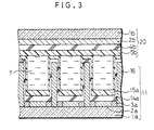
- Fig. 3 is a cross-sectional view that shows a schematic construction of a liquid crystal display element of another embodiment of the present invention.
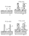
- Figs. 4(a) through 4(d) are cross-sectional view that show respective stages of a manufacturing process of the liquid crystal display element of Fig. 3.
- Fig. 5 is a cross-sectional view that shows a schematic construction of a liquid crystal display element that was manufactured by a conventional manufacturing process.
- Fig. 1 is a cross-sectional view that shows a schematic construction of a liquid crystal display element of one embodiment of the present invention.
- the liquid crystal display element is constituted by a pair of substrates 10 and 20 that are joined face to face with each other and liquid crystal 7 that is sealed in the gap in between.
- the substrate 10 is constituted by an insulating substrate la, a plurality of electrodes 2a that are placed in parallel with one another, light-shielding films 3a, an insulating film 4a that is formed in a manner so as to cover the insulating substrate 1a, the electrodes 2a and the light-shielding films 3a, spacers 6 that are formed on the surface of the insulating film 4a, and an alignment layer 5a that is formed in a manner so as to cover the surfaces of the insulating film 4a and the spacers 6.
- the substrate 20 is constituted by an insulating substrate 1b, a plurality of electrodes 2b that are placed in parallel with one another, an insulating film 4b, and an alignment layer 5b that is formed on the surface of the insulating layer 4b.
- the insulating substrates 1a and 1b are made of a transparent material such as glass or plastic. Further, transparent electrodes made of ITO (Indium Tin Oxide) are generally used as the electrodes 2a and 2b. However, the electrodes may be constituted by using other metals. Moreover, the light-shielding films 3a are made of metals, such as Cr, Mo and Al, opaque organic resins or other materials.
- ITO Indium Tin Oxide
- ferroelectric liquid crystal is used as the liquid crystal 7. Since ferroelectric liquid crystal has superior properties such as high-speed response and bistability, it becomes possible to display high-resolution images with a large capacity.
- the present liquid crystal display element having the above-mentioned arrangement is manufactured by the following processes. First, a film with a thickness of approximately 100 nm is formed on the surface of the insulating substrate 1a by using a metal such as molybdenum or an opaque organic resin, and this film is patterned by the photolithography so as to form light-shielding films 3a with a desired pattern, as shown in Fig. 2(a).
- an ITO film with a film thickness of approximately 100 nm is formed on the insulating substrate 1a by the sputtering method, and this film is patterned by the photolithography so as to form electrodes 2a.
- the resulting shape is shown in Fig. 2(b), wherein the light-shielding films 3a are placed along both sides of each electrode 2a.
- this insulating film 4a may be omitted depending on cases.
- the photoresist is irradiated with ultraviolet light by using a photomask only at portions thereof in which spacers are to be formed within regions that are located between the light-shielding films 3a and that have no electrodes 2a. Thereafter, non-exposed portions are removed, and as illustrated in Fig. 2(d), spacers 6 are formed by carrying out a baking process at approximately 145°C for 30 minutes. Additionally, the spacers 6 are formed to have a desired shape, such as a column shape, wall shape or striped shape, by changing the pattern and location of the photomask in various manners.
- a desired shape such as a column shape, wall shape or striped shape
- PSI-A-2101 manufactured by Chisso Corporation, is formed thereto so as to have a film thickness of 50 nm, and after this has been subjected to a pre-baking process at approximately 180°C for one hour, a rubbing process is applied to the surface thereof so as to form an alignment layer 5a as illustrated in Fig. 2(e).
- the substrate 10 is manufactured by the above-mentioned processes. Further, the substrate 20 is manufactured as follows: electrodes 2b, light-shielding films, not shown, and an insulating film 4b are successively formed on an insulating substrate 1b through the same processes as described above, and an alignment layer 5b is formed on the insulating film 4b.
- the substrates 10 and 20 are aligned face to face with each other so that their alignment layers 5a and 5b have the same rubbing directions, and the alignment layers films 5a and 5b are bonded to each other by applying a pressure of 0.6 kg/cm 2 at approximately 200°C for one hour. Further, liquid crystal 7 is sealed in the gap between the substrates 10 and 20; thus, a liquid crystal display element is formed.
- the liquid crystal display element manufactured by the above-mentioned processes, is allowed to have a uniform cell thickness with a precision within ⁇ 0.3 ⁇ m. Further, since the vicinity of the spacers 6 is shielded by the light-shielding films 3a and light-shielding films (not shown) on the substrate 20, uniform orientation and switching characteristics are obtained in the pixel display sections.
- spacers 6 organic resins, such as polyimide and acryl resin, and metals, such as Cr, Mo, Al, may be adopted in addition to the above-mentioned negative-working photoresist. Moreover, with respect to the formation of the spacers 6, they may be formed at any region on the insulating substrate la; however, it is preferable to form them at the other regions except for the pixel display regions so as not to deteriorate the display quality.
- the above description exemplifies an arrangement wherein the spacers 6 are formed only on the substrate 10; however, necessary spacers 6 may be formed on the respective substrates 10 and 20 in a separated manner, and the substrates 10 and 20 may be bonded to each other by allowing the alignment layer formed on the spacers 6 on one of the substrates 10 and 20 to adhere to the alignment layer located at regions without spacers on the other substrate.
- the insulating films 4a and 4b are not necessarily required, and they can be omitted as long as no leakage current appears between the substrates 10 and 20. Furthermore, in addition to the above-mentioned various films, an overcoat film and other films may be formed on demand.
- a pair of substrates 10 and 20 are provided, and one of the substrate 10 is designed as follows: after electrodes 2a and light-shielding films 3a and, if necessary, an insulating film 4a and other films have been formed on an insulating substrate la, spacers 6 are formed on these films, and then an alignment layer 5a is formed in a manner so as to cover the entire surface of the insulating substrate 1a including the spacers 6.
- the other substrate 20 is designed as follows: after electrodes 2b and, if necessary, an insulating film 4b have been formed on an insulating substrate 1b, an alignment layer 5b is formed in a manner so as to cover the entire surface of the insulating substrate 1b.
- the substrates 10 and 20 are bonded to each other by allowing the alignment layers 5a and 5b, both made of the same material, to be softened and to adhere to each other by applying heat and pressure.
- the spacers 6 are not softened even in this heat and pressure applying process; therefore, different from conventional arrangements, it is possible to prevent the substrate gap from becoming ununiform due to softening and deformation of the spacers, and consequently to control the gap between the substrates 10 and 20 with high precision.
- the paired substrates are bonded to each other by adhesion between the same materials, it is possible to avoid adverse effects, such as deformation or deterioration in one of -the materials and insufficient adhesive strength, which tend to occur in adhesion between different materials, such as adhesion between conventional alignment layer and spacers.
- the spacers 6 are made of a material having an optically isotropic property, that is, a material having no anisotropy in its refractive index, and when the alignment layer 5a on the spacers 6 is completely bonded to the alignment layer 5b on the opposing substrate 20 without a gap, the spacers 6 are allowed to extinct when seen through crossed Nicol-prisms.
- the spacers 6 since the spacers 6 also function as a black matrix, they shield the other portions except for the pixel display regions from light, thereby making it possible to improve the contrast.
- the liquid crystal 7 only contacts the alignment layers 5a and 5b, and is not allowed to contact the spacers 6.
- the orientation and switching characteristics of the liquid crystal tend to become ununiform due to the spacers, resulting in nonuniformity in display.
- the liquid crystal 7 since the liquid crystal 7 does not contact the spacers 6, its orientated state and switching characteristics are not adversely affected by the spacers 6; thus, it becomes possible to achieve a good display state without nonuniformity.
- the vicinity of the spacers 6 in the pixel display regions is shielded by the light-shielding films 3a; therefore, even if slight display nonuniformity occurs, the nonuniformity hardly gives adverse effects on the actual display state, thereby making it possible to provide high display quality.
- the substrate construction having superior shock resistance protects the liquid crystal 7 from external pressure.
- ferroelectric liquid crystal is used as the liquid crystal 7
- the resulting effect is that a liquid crystal display which allows for high-resolution image display with a large capacity by using ferroelectric liquid crystal can be put into practical use.
- the spacers 6 are formed prior to the formation of the alignment layer 5a, it is possible to prevent the alignment layer 5a from being contaminated or damaged by solvents or other materials that are used in the process for forming the spacers 6. Consequently, it is possible to provide a liquid crystal display element which can achieve good display quality without nonuniformity.
- Fig. 3 is a cross-sectional view showing a schematic construction of a liquid crystal display element of another embodiment of the present invention.
- the liquid crystal display element that was described in the aforementioned Embodiment 1 has an arrangement wherein the spacers 6 are formed on the insulating film 4a and the alignment layer 5a is formed in a manner so as to cover the surfaces of the insulating film 4a and the spacers 6.
- the liquid crystal display element of Embodiment 2 has an arrangement wherein a substrate 11, shown in Fig.
- spacers 16 are formed at portions on the surface of an insulating substrate la where neither electrodes 2a nor light-shielding films 3a are formed, and an insulating film 14a and an alignment layer 15a are successively formed in a manner so as to cover the electrodes 2a, the light-shielding films 3a and the spacers 16.
- the liquid crystal display element having the above-mentioned arrangement is manufactured by the following processes: First, the electrodes 2a and the light-shielding films 3a are formed on the surface of the insulating substrate 1a through the processes as illustrated in Figs. 2(a) and 2(b) in the aforementioned embodiment 1.
- Fig. 4(a) shows a state at the time when these processes have been completed.
- a photosensitive organic resin such as, for example, UR-3100 manufactured by Toray Industries Inc.
- the film thickness is adjusted so that it is set at 1.5 ⁇ m after a baking process.
- the photosensitive resin is irradiated with ultraviolet light by using a photomask only at portions thereof in which spacers are to be formed within regions that have no electrodes 2a and that are located between the light-shielding films 3a.
- spacers 16 are formed as illustrated in Fig. 4(b). Additionally, in this case also, as described in the aforementioned Embodiment 1, spacers 16 is formed to have a desired shape, such as a column shape, wall shape or striped shape, by changing the pattern and location of the photomask in various manners.
- SiO 2 is applied onto the surfaces of the electrodes 2a, the light-shielding films 3a and the spacers 16 by the spin coating method; thus, an insulating film 14a is formed as illustrated in Fig. 4(c).
- polyimide PSI-A-2101, manufactured by Chisso Corporation
- a rubbing process is applied to the surface thereof so as to form an alignment layer 15a as illustrated in Fig. 4(d).
- the substrate 11 is manufactured by the above-mentioned processes.
- the substrates 11 and 20 are bonded to each other in the same manner as the aforementioned Embodiment 1, and liquid crystal 7 is sealed into the gap between them; thus, a liquid crystal display element is formed.
- the liquid crystal display element of the present embodiment is distinct from that of the aforementioned Embodiment 1 in that the insulating film, which was formed in the process prior to the spacer-forming process in the aforementioned Embodiment 1, is formed in a process succeeding to the spacer-forming process.
- the alignment layer 15a is formed in a process after the formation of the spacers 16
- the substrates 11 and 20 are bonded to each other by allowing the alignment layers 15a and 5b, both made of the same material, to be softened and to adhere to each other by applying heat and pressure
- liquid crystal display element which was manufactured by conventional processes is taken as a comparative example, and is compared with the above-mentioned liquid crystal display elements of the present invention.
- the conventional liquid crystal display element has an arrangement wherein after an alignment layer 35a has been formed, spacers 36 are formed on the alignment layer 35a.
- the manufacturing processes of the conventional liquid crystal display element are as follows:
- ITO was formed on an insulating substrate 31a by the sputtering method as a film with a thickness of 100 nm, and this was patterned by the photolithography so as to form transparent electrodes 32a.
- SiO 2 was applied onto the electrodes 32a by the spin coating method so as to form an insulating film 34a.
- polyimide PSI-A-2101, manufactured by Chisso Corporation was applied onto the insulating film 34a so as to have a film thickness of 50 nm, and after this had been subjected to a baking process at approximately 200°C for one hour, an alignment layer 35a was formed.
- photosensitive organic resin (UR-3100 manufactured by Toray Industries Inc.) by the spin coating method.
- the film thickness was adjusted so that it was set to 1.5 ⁇ m after a baking process.
- a photomask had been placed at portions at which no electrodes 2a were formed, this was irradiated with ultraviolet light, and the non-exposed portions were removed. Furthermore, this was subjected to a baking process at approximately 300°C for one hour; thus, spacers 36 were formed.
- the alignment layer 35a was subjected to a rubbing process; thus, a substrate 30 was completed. Further, the substrate 40 was formed by successively forming electrodes 32b, an insulating film 34b and an alignment layer 35b on the insulating substrate 31b in the same manner as described above.
- the substrates 30 and 40 were bonded to each other with the same rubbing directions, and the upper surface of the spacers 36 and the surface of the alignment layer 35b were allowed to adhere each other by applying a pressure of 0.6 kg/cm 2 at approximately 350°C for one hour. Further, liquid crystal 37 was sealed in the gap in between; thus, a liquid crystal display element was formed.
- the present invention is not intended to be limited by the aforementioned Embodiments, and various modifications are available within the scope of the present invention.
- transparent glass or plastic substrates are used as the insulating substrates 1a and 1b; however, any substrates may be adopted as long as at least one substrate has a light-transmitting property.
- the liquid crystal 7 is not intended to be limited to ferroelectric liquid crystal, and various liquid crystal material may be adopted.
Abstract
Description
- The present invention relates to a liquid crystal display element which has a substrate structure capable of achieving a uniform cell thickness and sufficient shock resistance, as well as to a manufacturing method thereof.
- Conventionally, liquid crystal display elements, which are made by bonding a paired substrates to each other with their electrode-bearing surfaces facing inside and by sealing liquid crystal into the gap between them, have been well known. In such liquid crystal displays, when the distance between the opposing substrates varies due to deformation of the substrates caused by external pressure or other adverse effects, changes in the threshold-voltage value, short circuit in the electrodes between the opposing substrates, disturbance in the orientation of the liquid crystal molecules, etc. tend to occur, thereby making it impossible to provide good display images. For this reason, in order to keep the distance between the paired substrates constant, some methods for placing spacers between the substrates have been suggested; conventionally, either of the following two methods is commonly adopted: (1) a method for spraying spherical particles and (2) a method for forming pillars made of an organic or inorganic material.
- Specific examples of the method (1) include a dry method in which spherical fine particles, made of, for example, an organic resin, such as a polymer of divinylbenzenes, are dispersed in a gas flow of nitrogen and then sprayed on the substrates, and a method in which the spherical fine particles are mixed in an alcohol solution or other solutions and sprayed on the substrates in a mist state.
- However, method (1) has the following problems: The first problem is that since the fine particles have a coagulating property whereby they coagulate with one another, it is difficult to spray them on the substrates in a uniform manner and consequently to achieve a uniform cell thickness. The second problem is that since it is difficult to control the adherence location of the fine particles, the particles, which have been unintentionally sprayed on pixels, tend to cause defects in the orientation, resulting in low display quality. Further, the third problem is that since the substrates are supported by the spherical fine particles that function as spacers only at their contact points, it is difficult to obtain sufficient strength against external pressure.
- Moreover, method (2) more specifically refers to a method in which: an organic or inorganic film is formed with a desired thickness, a resist film is formed thereon, and the resist film is irradiated by ultraviolet lights using a photomask, thereby forming pillars that function as spacers. Here, instead of the resist film, for example, photosensitive organic resins, such as photosensitive polyimide or photosensitive acryl resins, can be adopted.
- As described above, advantages of method (2) are that the pillars can be selectively formed on the outside of the pixels, and that the contact surfaces between the substrates and the pillars can be shaped into a desired pattern. Thus, method (2) is superior in the uniformity of the cell thickness, the strength against external pressure, and display quality, as compared with method (1).
- Recently, ferroelectric liquid crystal has been taken notice of as a prospective liquid crystal material since it has superior properties, such as having spontaneous polarization and providing high-speed response. However, the disadvantage of ferroelectric liquid crystal is that since it has a structure whose molecule-regularity is closer to that of a crystal, once the molecular orientation has been disturbed, it is difficult to return to its original state, that is, it is susceptible to shock. For this reason, in order to solve the above-mentioned inherent problem with ferroelectric liquid crystal, it is essential to provide a substrate construction that is superior in shock resistance. In order to provide a method for manufacturing such a liquid crystal display element, method (2) is considered to be a more prospective candidate than method (1).
- In general, in the conventional manufacturing method (2), after an alignment layer has been formed on an insulating substrate, spacers are formed on the alignment layer. However, the conventional manufacturing methods have the following various problems.
- First, the manufacturing process of the spacers may give adverse effects, such as contamination, deterioration, and damage, on the alignment layer. Conventionally, in general, spacers are formed on a substrate that has been subjected to an alignment process, by using a photolithography process wherein photosensitive polyimide, photoresist and other materials are used. Here, solvents, which are used in the photolithography process, tend to give adverse effects on the alignment layer. In this case, since the alignment capability of the alignment layer is lowered, the orientation of liquid crystal molecules becomes ununiform, thereby causing degradation in the display quality.
- Moreover, when consideration is given so that spacer materials do not affect the alignment layer, limitations, such as a limitation that spacer materials having a setting temperature higher than the alignment layer can not be used, have to be imposed on the spacer materials.
- Furthermore, in the above-mentioned conventional manufacturing method, when the substrates are bonded to each other, the spacers that have been formed on one of the substrates and the alignment layer that has been formed on the opposing substrate are bonded to each other. Here, such a bonding process between the materials of different types raises the following problems: The bonding process is carried out while both of the spacers and the alignment layer are being softened by applying heat under pressure; therefore, when there is a great difference between the respective softening temperatures of the spacers and the alignment layer, the material having the lower softening temperature may not retain its shape upon having a temperature rise to the higher softening temperature. Consequently, for example, if the spacers are deformed, those spacers may enter the pixel portions, thereby causing problems, such as degradation in the display quality and low precision in the cell-thickness control. In contrast, if a sufficient temperature rise is not provided, a sufficient adhesive strength may not be obtained, thereby making the substrates susceptible to deformation under external pressure.
- The objective of the present invention is to provide a liquid crystal display element which has a uniform cell thickness and a sufficient shock resistance so that it can achieve good display quality without nonuniformity.
- In order to achieve the above-mentioned objective, the liquid crystal display element of the present invention, which has a pair of substrates at least one of which has a light-transmitting property, liquid crystal, alignment layers that are respectively formed on the pair of the substrates, and a spacer that is formed on at least one of the pair of the substrates, is designed so that: the alignment layer is formed so as to cover at least the spacer on the surface of the substrate; and a portion of the alignment layer, which is located on the spacer, is bonded to the alignment layer on the other substrate.
- In the above-mentioned arrangement, the paired substrates are bonded to each other by the adhesion between the two alignment layers. For this reason, it is possible to easily control the applications of heat and pressure during the bonding process, thereby making the cell thickness uniform, as well as improving the adhesive strength. In other words, it becomes possible to avoid adverse effects, such as deformation of either of the materials due to applications of unnecessarily high heat and pressure and insufficient adhesive strength due to applications of insufficient heat and pressure, which conventionally tend to occur, when the spacer on one of the substrates and the alignment layer on the other substrate are bonded to each other. Thus, it becomes possible to provide a liquid crystal display element which has superior shock resistance and can achieve good display quality without nonuniformity.
- Moreover, in the liquid crystal display element, when the liquid crystal is made of ferroelectric liquid crystal, it is possible to provide a further high-resolution display, since high-speed response is available that is one of the superior properties of ferroelectric liquid crystal. Here, ferroelectric liquid crystal has a higher ordered molecular orientation that is closer to crystal, for example, as compared with nematic liquid crystal. Therefore, the disadvantage of ferroelectric liquid crystal is that, once the molecular orientation has been disturbed due to external pressure, it is difficult to return to its original state, that is, it is susceptible to shock. However, the above-mentioned arrangement, which has an improved substrate strength, can eliminate this disadvantage. Thus, it is possible to achieve a liquid crystal display element which allows the ferroelectric liquid crystal to exhibit its superior properties.
- In order to achieve the aforementioned objective, the manufacturing method of a liquid crystal display element of the present invention is provided with the steps of forming a spacer on an insulating substrate and forming an alignment layer in a manner so as to cover the spacer.
- In the above-mentioned manufacturing method, a spacer is first formed on an insulating substrate. Here, before or after this process, members, such as electrodes, a light-shielding film, or an insulating film, may be formed on the insulating substrate, if necessary. Thereafter, an alignment layer is formed in a manner so as to cover the spacer. As described above, since the spacer is formed prior to the formation of the alignment layer, it is possible to prevent the alignment layer from being contaminated or damaged by solvents or other materials that are used in the spacer-forming process. With this arrangement, it is possible to provide a liquid crystal display element which can achieve good display quality without nonuniformity. Moreover, in the case when the spacer and alignment layer are formed by a baking process, this arrangement makes it possible to use spacer materials such as those require a baking temperature higher than that of the alignment layer.
- For a fuller understanding of the nature and advantages of the invention, reference should be made to the ensuing detailed description taken in conjunction with the accompanying drawings.
- Fig. 1 is a cross-sectional view that shows a schematic construction of a liquid crystal display element of one embodiment of the present invention.
- Figs. 2(a) through 2(e) are cross-sectional views that show respective stages of a manufacturing process of the liquid crystal display element.
- Fig. 3 is a cross-sectional view that shows a schematic construction of a liquid crystal display element of another embodiment of the present invention.
- Figs. 4(a) through 4(d) are cross-sectional view that show respective stages of a manufacturing process of the liquid crystal display element of Fig. 3.
- Fig. 5 is a cross-sectional view that shows a schematic construction of a liquid crystal display element that was manufactured by a conventional manufacturing process.
- Referring to Figs. 1 and 2, the following description will discuss one embodiment of the present invention.
- Fig. 1 is a cross-sectional view that shows a schematic construction of a liquid crystal display element of one embodiment of the present invention. The liquid crystal display element is constituted by a pair of
substrates - The
substrate 10 is constituted by an insulating substrate la, a plurality ofelectrodes 2a that are placed in parallel with one another, light-shielding films 3a, aninsulating film 4a that is formed in a manner so as to cover the insulating substrate 1a, theelectrodes 2a and the light-shielding films 3a,spacers 6 that are formed on the surface of theinsulating film 4a, and analignment layer 5a that is formed in a manner so as to cover the surfaces of theinsulating film 4a and thespacers 6. - Further, the
substrate 20 is constituted by an insulating substrate 1b, a plurality ofelectrodes 2b that are placed in parallel with one another, an insulating film 4b, and analignment layer 5b that is formed on the surface of the insulating layer 4b. - The insulating substrates 1a and 1b are made of a transparent material such as glass or plastic. Further, transparent electrodes made of ITO (Indium Tin Oxide) are generally used as the
electrodes shielding films 3a are made of metals, such as Cr, Mo and Al, opaque organic resins or other materials. - In this embodiment, a ferroelectric liquid crystal is used as the liquid crystal 7. Since ferroelectric liquid crystal has superior properties such as high-speed response and bistability, it becomes possible to display high-resolution images with a large capacity.
- The present liquid crystal display element having the above-mentioned arrangement is manufactured by the following processes. First, a film with a thickness of approximately 100 nm is formed on the surface of the insulating substrate 1a by using a metal such as molybdenum or an opaque organic resin, and this film is patterned by the photolithography so as to form light-shielding
films 3a with a desired pattern, as shown in Fig. 2(a). - Next, an ITO film with a film thickness of approximately 100 nm is formed on the insulating substrate 1a by the sputtering method, and this film is patterned by the photolithography so as to form
electrodes 2a. The resulting shape is shown in Fig. 2(b), wherein the light-shieldingfilms 3a are placed along both sides of eachelectrode 2a. - Further, to this is applied SiO2 by the spin coating method so as to form an insulating
film 4a having a uniform surface, as illustrated in Fig. 2(c). Here, this insulatingfilm 4a may be omitted depending on cases. - Onto the insulating
film 4a is applied negative-working photoresist, such as OMR-83 manufactured by Tokyo Ohka Kogyo Co., Ltd., by the spin coating method so that it has a film thickness of 1.5 µm after a baking process. Next, the photoresist is irradiated with ultraviolet light by using a photomask only at portions thereof in which spacers are to be formed within regions that are located between the light-shieldingfilms 3a and that have noelectrodes 2a. Thereafter, non-exposed portions are removed, and as illustrated in Fig. 2(d),spacers 6 are formed by carrying out a baking process at approximately 145°C for 30 minutes. Additionally, thespacers 6 are formed to have a desired shape, such as a column shape, wall shape or striped shape, by changing the pattern and location of the photomask in various manners. - Next, PSI-A-2101, manufactured by Chisso Corporation, is formed thereto so as to have a film thickness of 50 nm, and after this has been subjected to a pre-baking process at approximately 180°C for one hour, a rubbing process is applied to the surface thereof so as to form an
alignment layer 5a as illustrated in Fig. 2(e). - The
substrate 10 is manufactured by the above-mentioned processes. Further, thesubstrate 20 is manufactured as follows:electrodes 2b, light-shielding films, not shown, and an insulating film 4b are successively formed on an insulating substrate 1b through the same processes as described above, and analignment layer 5b is formed on the insulating film 4b. - Next, the
substrates alignment layers films substrates - The liquid crystal display element, manufactured by the above-mentioned processes, is allowed to have a uniform cell thickness with a precision within ± 0.3 µm. Further, since the vicinity of the
spacers 6 is shielded by the light-shieldingfilms 3a and light-shielding films (not shown) on thesubstrate 20, uniform orientation and switching characteristics are obtained in the pixel display sections. - Here, with respect to the material of
spacers 6, organic resins, such as polyimide and acryl resin, and metals, such as Cr, Mo, Al, may be adopted in addition to the above-mentioned negative-working photoresist. Moreover, with respect to the formation of thespacers 6, they may be formed at any region on the insulating substrate la; however, it is preferable to form them at the other regions except for the pixel display regions so as not to deteriorate the display quality. - Additionally, the above description exemplifies an arrangement wherein the
spacers 6 are formed only on thesubstrate 10; however,necessary spacers 6 may be formed on therespective substrates substrates spacers 6 on one of thesubstrates - Moreover, the insulating
films 4a and 4b are not necessarily required, and they can be omitted as long as no leakage current appears between thesubstrates - As described above, in the liquid crystal display element of Embodiment 1, a pair of
substrates substrate 10 is designed as follows: afterelectrodes 2a and light-shieldingfilms 3a and, if necessary, an insulatingfilm 4a and other films have been formed on an insulating substrate la,spacers 6 are formed on these films, and then analignment layer 5a is formed in a manner so as to cover the entire surface of the insulating substrate 1a including thespacers 6. Theother substrate 20 is designed as follows: afterelectrodes 2b and, if necessary, an insulating film 4b have been formed on an insulating substrate 1b, analignment layer 5b is formed in a manner so as to cover the entire surface of the insulating substrate 1b. - Further, the
substrates spacers 6 are not softened even in this heat and pressure applying process; therefore, different from conventional arrangements, it is possible to prevent the substrate gap from becoming ununiform due to softening and deformation of the spacers, and consequently to control the gap between thesubstrates - Moreover, since the paired substrates are bonded to each other by adhesion between the same materials, it is possible to avoid adverse effects, such as deformation or deterioration in one of -the materials and insufficient adhesive strength, which tend to occur in adhesion between different materials, such as adhesion between conventional alignment layer and spacers. In other words, it is possible to easily control the applications of heat and pressure during the bonding process, thereby making the cell thickness uniform, as compared with the adhesion between different materials. Further, it is possible to further improve the adhesive strength. Consequently, it becomes possible to provide a liquid crystal display element which can achieve good display quality without nonuniformity and which has superior shock resistance.
- Moreover, when the
spacers 6 are made of a material having an optically isotropic property, that is, a material having no anisotropy in its refractive index, and when thealignment layer 5a on thespacers 6 is completely bonded to thealignment layer 5b on the opposingsubstrate 20 without a gap, thespacers 6 are allowed to extinct when seen through crossed Nicol-prisms. In other words, under the above conditions, since thespacers 6 also function as a black matrix, they shield the other portions except for the pixel display regions from light, thereby making it possible to improve the contrast. - Furthermore, as clearly indicated by Fig. 1, the liquid crystal 7 only contacts the alignment layers 5a and 5b, and is not allowed to contact the
spacers 6. In conventional liquid crystal display elements wherein the spacers are in contact with the liquid crystal, the orientation and switching characteristics of the liquid crystal tend to become ununiform due to the spacers, resulting in nonuniformity in display. However, in the arrangement of the present Embodiment 1, since the liquid crystal 7 does not contact thespacers 6, its orientated state and switching characteristics are not adversely affected by thespacers 6; thus, it becomes possible to achieve a good display state without nonuniformity. Further, the vicinity of thespacers 6 in the pixel display regions is shielded by the light-shieldingfilms 3a; therefore, even if slight display nonuniformity occurs, the nonuniformity hardly gives adverse effects on the actual display state, thereby making it possible to provide high display quality. - Moreover, in the arrangement of the present embodiment, the substrate construction having superior shock resistance protects the liquid crystal 7 from external pressure. In other words, even when ferroelectric liquid crystal is used as the liquid crystal 7, it is possible to eliminate the inherent disadvantage of the ferroelectric liquid crystal, that is, the susceptibility to external pressure. The resulting effect is that a liquid crystal display which allows for high-resolution image display with a large capacity by using ferroelectric liquid crystal can be put into practical use.
- Furthermore, since the
spacers 6 are formed prior to the formation of thealignment layer 5a, it is possible to prevent thealignment layer 5a from being contaminated or damaged by solvents or other materials that are used in the process for forming thespacers 6. Consequently, it is possible to provide a liquid crystal display element which can achieve good display quality without nonuniformity. - Referring mainly to Figs. 3 and 4, the following description will discuss another embodiment of the present invention. Here, those members that have the same functions and that are described in the aforementioned embodiment are indicated by the same reference numerals and the detailed description thereof is omitted.
- Fig. 3 is a cross-sectional view showing a schematic construction of a liquid crystal display element of another embodiment of the present invention. The liquid crystal display element that was described in the aforementioned Embodiment 1 has an arrangement wherein the
spacers 6 are formed on the insulatingfilm 4a and thealignment layer 5a is formed in a manner so as to cover the surfaces of the insulatingfilm 4a and thespacers 6. Here, the liquid crystal display element of Embodiment 2 has an arrangement wherein asubstrate 11, shown in Fig. 3, is constituted as follows: spacers 16 are formed at portions on the surface of an insulating substrate la where neitherelectrodes 2a nor light-shieldingfilms 3a are formed, and an insulatingfilm 14a and analignment layer 15a are successively formed in a manner so as to cover theelectrodes 2a, the light-shieldingfilms 3a and thespacers 16. - The liquid crystal display element having the above-mentioned arrangement is manufactured by the following processes: First, the
electrodes 2a and the light-shieldingfilms 3a are formed on the surface of the insulating substrate 1a through the processes as illustrated in Figs. 2(a) and 2(b) in the aforementioned embodiment 1. Fig. 4(a) shows a state at the time when these processes have been completed. - Next, onto the insulating substrate 1a on which the
electrodes 2a and the light-shieldingfilms 3a have been formed is applied a photosensitive organic resin, such as, for example, UR-3100 manufactured by Toray Industries Inc., by the spin coating method. Here, in this application process, the film thickness is adjusted so that it is set at 1.5 µm after a baking process. Successively, the photosensitive resin is irradiated with ultraviolet light by using a photomask only at portions thereof in which spacers are to be formed within regions that have noelectrodes 2a and that are located between the light-shieldingfilms 3a. Thereafter, non-exposed portions are removed, and a baking process is carried out at approximately 300°C for 1 hour; thus, spacers 16 are formed as illustrated in Fig. 4(b). Additionally, in this case also, as described in the aforementioned Embodiment 1,spacers 16 is formed to have a desired shape, such as a column shape, wall shape or striped shape, by changing the pattern and location of the photomask in various manners. - Next, SiO2 is applied onto the surfaces of the
electrodes 2a, the light-shieldingfilms 3a and thespacers 16 by the spin coating method; thus, an insulatingfilm 14a is formed as illustrated in Fig. 4(c). Further, polyimide (PSI-A-2101, manufactured by Chisso Corporation) is applied onto the insulatingfilm 14a so as to have a film thickness of 50 nm, and after this has been subjected to a pre-baking process at approximately 180°C for one hour, a rubbing process is applied to the surface thereof so as to form analignment layer 15a as illustrated in Fig. 4(d). Thesubstrate 11 is manufactured by the above-mentioned processes. - Next, the
substrates - As described above, the liquid crystal display element of the present embodiment is distinct from that of the aforementioned Embodiment 1 in that the insulating film, which was formed in the process prior to the spacer-forming process in the aforementioned Embodiment 1, is formed in a process succeeding to the spacer-forming process. However, with respect to the operation wherein the
alignment layer 15a is formed in a process after the formation of thespacers 16, and to the operation wherein thesubstrates substrates - Here, a liquid crystal display element which was manufactured by conventional processes is taken as a comparative example, and is compared with the above-mentioned liquid crystal display elements of the present invention.
- As illustrated in Fig. 5, the conventional liquid crystal display element has an arrangement wherein after an
alignment layer 35a has been formed,spacers 36 are formed on thealignment layer 35a. The manufacturing processes of the conventional liquid crystal display element are as follows: - First, ITO was formed on an insulating substrate 31a by the sputtering method as a film with a thickness of 100 nm, and this was patterned by the photolithography so as to form
transparent electrodes 32a. Next, SiO2 was applied onto theelectrodes 32a by the spin coating method so as to form an insulatingfilm 34a. Further, polyimide (PSI-A-2101, manufactured by Chisso Corporation) was applied onto the insulatingfilm 34a so as to have a film thickness of 50 nm, and after this had been subjected to a baking process at approximately 200°C for one hour, analignment layer 35a was formed. - Next, onto the
alignment layer 35a, is applied photosensitive organic resin (UR-3100 manufactured by Toray Industries Inc.) by the spin coating method. Here, upon the application process, the film thickness was adjusted so that it was set to 1.5 µm after a baking process. Next, after a photomask had been placed at portions at which noelectrodes 2a were formed, this was irradiated with ultraviolet light, and the non-exposed portions were removed. Furthermore, this was subjected to a baking process at approximately 300°C for one hour; thus, spacers 36 were formed. - After the formation of the
spacers 36, thealignment layer 35a was subjected to a rubbing process; thus, asubstrate 30 was completed. Further, thesubstrate 40 was formed by successively formingelectrodes 32b, an insulating film 34b and analignment layer 35b on the insulatingsubstrate 31b in the same manner as described above. - Next, the
substrates spacers 36 and the surface of thealignment layer 35b were allowed to adhere each other by applying a pressure of 0.6 kg/cm2 at approximately 350°C for one hour. Further,liquid crystal 37 was sealed in the gap in between; thus, a liquid crystal display element was formed. - When comparisons were made between the liquid crystal display element that was made by the above-mentioned conventional processes and liquid crystal display elements of the aforementioned Embodiments, it was found that the liquid crystal display elements of the aforementioned Embodiments were superior in both the uniformity of the cell thickness and the adhesive strength of the substrates.
- The present invention is not intended to be limited by the aforementioned Embodiments, and various modifications are available within the scope of the present invention. For example, in the above-mentioned examples, transparent glass or plastic substrates are used as the insulating substrates 1a and 1b; however, any substrates may be adopted as long as at least one substrate has a light-transmitting property. Further, the liquid crystal 7 is not intended to be limited to ferroelectric liquid crystal, and various liquid crystal material may be adopted.
- Moreover, another method may be adopted, wherein only a pre-baking process is carried out when alignment layers are respectively formed on the paired substrates and when these substrates are bonded to each other, a baking process is carried out with pressure and heat being applied thereto. This method also makes it possible to provide liquid crystal display elements which are superior in both the uniformity of the cell thickness and the adhesive strength of the substrates.
- The invention being thus described, it will be obvious that the same may be varied in many ways. Such variations are not to be regarded as a departure from the spirit and scope of the invention, and all such modifications as would be obvious to one skilled in the art are intended to be included within the scope of the following claims.
Claims (17)
- A liquid crystal display element comprising:a pair of substrates at least one of which has a light-transmitting property;liquid crystal;alignment layers that are respectively formed on the pair of the substrates; anda spacer that is formed on at least one of the pair of the substrates,wherein: the alignment layer is formed so as to cover at least the spacer on the surface of the substrate; and a portion of the alignment layer, which is located on the spacer, is bonded to the alignment layer on the other substrate.
- The liquid crystal display element as defined in claim 1, wherein the liquid crystal is ferroelectric liquid crystal.
- The liquid crystal display element as defined in claim 1, wherein the spacer has a wall shape.
- The liquid crystal display element as defined in claim 1, wherein the spacer has a column shape.
- The liquid crystal display element as defined in claim 1, wherein the spacer is formed outside of pixel regions.
- The liquid crystal display element as defined in claim 1, further comprising light-shielding films for shielding the vicinity of the spacer from light.
- The liquid crystal display element as defined in claim 1, wherein the spacer is made of a material including an organic resin.
- The liquid crystal display element as defined in claim 1, wherein the spacer is made of a material including photoresist.
- The liquid crystal display element as defined in claim 1, wherein the spacer is made of a material including a metal.
- The liquid crystal display element as defined in claim 1, wherein the alignment layers, which are respectively formed on the pair of the substrates, are made of the same material.
- The liquid crystal display element as defined in claim 1, wherein the spacer has a light-shielding property.
- The liquid crystal display element as defined in claim 1, wherein the spacer has an optically isotropic property.
- The liquid crystal display element as defined in claim 1, further comprising an insulating film that covers entire surface of the spacer, wherein the alignment layer is formed in a manner so as to cover the insulating film.
- A manufacturing method of a liquid crystal display element comprising the steps of:forming a spacer on a first insulating substrate; andforming an alignment layer in a manner so as to cover the spacer.
- The manufacturing method of a liquid crystal display element as defined in claim 14, wherein the spacer-forming process comprises a step of baking a spacer material and the alignment-layer-forming process comprises a step of baking an alignment-layer material.
- The manufacturing method of a liquid crystal display element as defined in claim 14, further comprising the steps of:forming at least an alignment layer on a second insulating substrate; andafter having placed the first and second insulating substrates so that the respective alignment layers face each other, allowing the alignment layers to adhere to each other while heat and pressure being applied.
- The manufacturing method of a liquid crystal display element as defined in claim 14, wherein: the process, which respectively forms the alignment layers on the first and second insulating substrates, further comprises a step of baking an alignment-layer material; and the process, which allows the alignment layers of the first and second insulating substrates to adhere to each other, is carried out at a temperature at which the alignment-layer material is subjected to a baking.
Applications Claiming Priority (3)
| Application Number | Priority Date | Filing Date | Title |
|---|---|---|---|
| JP28768095 | 1995-11-06 | ||
| JP287680/95 | 1995-11-06 | ||
| JP7287680A JPH09127525A (en) | 1995-11-06 | 1995-11-06 | Liquid crystal display device and preparation thereof |
Publications (2)
| Publication Number | Publication Date |
|---|---|
| EP0772071A1 true EP0772071A1 (en) | 1997-05-07 |
| EP0772071B1 EP0772071B1 (en) | 2003-06-18 |
Family
ID=17720340
Family Applications (1)
| Application Number | Title | Priority Date | Filing Date |
|---|---|---|---|
| EP96308051A Expired - Lifetime EP0772071B1 (en) | 1995-11-06 | 1996-11-06 | Liquid crystal display element and fabrication process thereof |
Country Status (4)
| Country | Link |
|---|---|
| US (1) | US5880803A (en) |
| EP (1) | EP0772071B1 (en) |
| JP (1) | JPH09127525A (en) |
| DE (1) | DE69628715T2 (en) |
Cited By (11)
| Publication number | Priority date | Publication date | Assignee | Title |
|---|---|---|---|---|
| EP0807846A2 (en) * | 1996-05-16 | 1997-11-19 | TryOnics Corporation | Color Display and its manufacturing method |
| FR2760542A1 (en) * | 1997-01-31 | 1998-09-11 | Nat Science Council | Closed cavity liquid crystal cell |
| EP0964287A1 (en) * | 1998-06-12 | 1999-12-15 | Asulab S.A. | Electro-optical liquid crystal display device and method of manufacturing of the same |
| EP0990942A1 (en) * | 1998-03-19 | 2000-04-05 | Matsushita Electric Industrial Co., Ltd. | Liquid crystal display device and method of manufacturing the same |
| EP1081536A2 (en) * | 1999-08-03 | 2001-03-07 | Minolta Co., Ltd. | Method of manufacturing a liquid crystal display |
| GB2319855B (en) * | 1996-11-28 | 2001-04-18 | Sharp Kk | Liquid crystal display element and method of manufacturing same |
| GB2356259A (en) * | 1996-11-28 | 2001-05-16 | Sharp Kk | Spacers for liquid crystal devices |
| US6449028B1 (en) | 1998-06-12 | 2002-09-10 | Asulab S.A. | Liquid crystal display device having sealing frame and/or spacers formed of anisotropic polymer used to align the liquid crystal molecules |
| WO2005024503A1 (en) * | 2003-09-04 | 2005-03-17 | Koninklijke Philips Electronics N.V. | Display device with spacers and seals and the method of manufacture thereof |
| US8045125B2 (en) | 1997-05-22 | 2011-10-25 | Semiconductor Energy Laboratory Co., Ltd. | Liquid crystal display device having a gap retaining member made of resin formed directly over the driver circuit |
| WO2023082364A1 (en) * | 2021-11-15 | 2023-05-19 | 武汉华星光电技术有限公司 | Display panel and display apparatus |
Families Citing this family (40)
| Publication number | Priority date | Publication date | Assignee | Title |
|---|---|---|---|---|
| JPH09127516A (en) * | 1995-11-06 | 1997-05-16 | Sharp Corp | Production of liquid crystal display element |
| KR0182876B1 (en) | 1996-01-09 | 1999-05-01 | 구자홍 | Method for controlling pretilt direction for lcd cell |
| JPH10153785A (en) * | 1996-09-26 | 1998-06-09 | Toshiba Corp | Liquid crystal display device |
| US6191836B1 (en) * | 1996-11-07 | 2001-02-20 | Lg Philips Lcd, Co., Ltd. | Method for fabricating a liquid crystal cell |
| US6292296B1 (en) | 1997-05-28 | 2001-09-18 | Lg. Philips Lcd Co., Ltd. | Large scale polarizer and polarizer system employing it |
| JPH10332923A (en) * | 1997-05-30 | 1998-12-18 | Sharp Corp | Color filter and liquid crystal display device |
| US6195147B1 (en) * | 1997-08-01 | 2001-02-27 | Canon Kabushiki Kaisha | Liquid crystal substrate with optical modulation region having different alignment control forces |
| US6208402B1 (en) * | 1997-09-17 | 2001-03-27 | Citizen Watch Co., Ltd. | Antiferroelectric liquid crystal panel |
| JPH11119227A (en) * | 1997-10-13 | 1999-04-30 | Hitachi Ltd | Liquid crystal display device |
| KR100259258B1 (en) | 1997-11-21 | 2000-06-15 | 구본준 | Liquid crystal display device |
| JP3456896B2 (en) * | 1997-12-25 | 2003-10-14 | シャープ株式会社 | Liquid crystal display |
| JP3481843B2 (en) * | 1997-12-26 | 2003-12-22 | シャープ株式会社 | Liquid crystal display |
| US7061679B1 (en) | 1998-05-27 | 2006-06-13 | Lg. Philips Lcd Co., Ltd. | Light irradiating device |
| JP3568862B2 (en) * | 1999-02-08 | 2004-09-22 | 大日本印刷株式会社 | Color liquid crystal display |
| KR100301853B1 (en) | 1999-03-25 | 2001-09-26 | 구본준, 론 위라하디락사 | Alignment layer for liquid crystal display device |
| KR100357214B1 (en) | 1999-04-21 | 2002-10-18 | 엘지.필립스 엘시디 주식회사 | Liquid crystal display device |
| JP4298131B2 (en) * | 1999-05-14 | 2009-07-15 | 株式会社半導体エネルギー研究所 | Method for manufacturing liquid crystal display device |
| US6400440B1 (en) * | 1999-06-23 | 2002-06-04 | International Business Machines Corporation | Passive liquid crystal display having pre-tilt control structure and light absorbent material at a center |
| TW459275B (en) | 1999-07-06 | 2001-10-11 | Semiconductor Energy Lab | Semiconductor device and method of fabricating the same |
| JP4666723B2 (en) | 1999-07-06 | 2011-04-06 | 株式会社半導体エネルギー研究所 | Method for manufacturing semiconductor device |
| US7084087B2 (en) * | 1999-09-07 | 2006-08-01 | Abb Lummus Global Inc. | Zeolite composite, method for making and catalytic application thereof |
| KR100475107B1 (en) | 1999-10-14 | 2005-03-09 | 엘지.필립스 엘시디 주식회사 | A method of manufacturing a multi-domain liquid crystal display device |
| JP2002023164A (en) * | 2000-07-04 | 2002-01-23 | Nec Corp | Method for liquid crystal displaying, liquid crystal display device and device for manufacturing the same |
| JP3936126B2 (en) | 2000-08-30 | 2007-06-27 | シャープ株式会社 | Transflective liquid crystal display device |
| KR100595300B1 (en) * | 2000-10-28 | 2006-07-03 | 엘지.필립스 엘시디 주식회사 | Photo-alignment Material and Liquid Crystal Display Device fabricated with it |
| KR100565739B1 (en) | 2000-10-28 | 2006-03-29 | 엘지.필립스 엘시디 주식회사 | Photo-alignment Characteristic Material and Liquid Crystal Display Device fabricated with it |
| KR100685943B1 (en) * | 2000-11-28 | 2007-02-23 | 엘지.필립스 엘시디 주식회사 | Method for fabricating smetic liquid crystal display device |
| US6795138B2 (en) * | 2001-01-11 | 2004-09-21 | Sipix Imaging, Inc. | Transmissive or reflective liquid crystal display and novel process for its manufacture |
| KR20020095509A (en) * | 2001-06-14 | 2002-12-27 | 주식회사 현대 디스플레이 테크놀로지 | Method for sealing liquid crystal display |
| EP1271225A1 (en) * | 2001-06-22 | 2003-01-02 | Hewlett-Packard Company, A Delaware Corporation | Bistable nematic liquid crystal device |
| KR100710163B1 (en) * | 2002-11-28 | 2007-04-20 | 엘지.필립스 엘시디 주식회사 | method for manufacturing of LCD |
| KR20050049986A (en) * | 2003-11-24 | 2005-05-27 | 엘지.필립스 엘시디 주식회사 | Color filter sustrate and fabrication method thereof using back exposure |
| TWI345118B (en) * | 2005-04-19 | 2011-07-11 | Ind Tech Res Inst | Module display component and manufacturing method for the same |
| KR20060110936A (en) | 2005-04-20 | 2006-10-26 | 엘지.필립스 엘시디 주식회사 | Liquid crystal display device and method for manufacturing the same |
| KR101021696B1 (en) * | 2005-05-19 | 2011-03-15 | 다이니폰 인사츠 가부시키가이샤 | Liquid crystal display element |
| US7911562B2 (en) * | 2005-05-19 | 2011-03-22 | Dai Nippon Printing Co., Ltd. | Liquid crystal display and process for producing the same |
| JP2006330490A (en) * | 2005-05-27 | 2006-12-07 | Sharp Corp | Liquid crystal display and its manufacturing method |
| KR101326575B1 (en) * | 2005-12-30 | 2013-11-08 | 엘지디스플레이 주식회사 | Method for fabricating color filter of liquid crystal display device |
| KR20070079184A (en) * | 2006-02-01 | 2007-08-06 | 삼성전자주식회사 | Liquid crystal display and method for fabricating the same |
| KR101742192B1 (en) * | 2011-01-31 | 2017-06-16 | 삼성디스플레이 주식회사 | Display panel and method of manufacturing the same |
Citations (4)
| Publication number | Priority date | Publication date | Assignee | Title |
|---|---|---|---|---|
| WO1986005283A1 (en) * | 1985-03-05 | 1986-09-12 | American Telephone & Telegraph Company | Thin, uniform electro-optic display |
| US4653864A (en) * | 1986-02-26 | 1987-03-31 | Ovonic Imaging Systems, Inc. | Liquid crystal matrix display having improved spacers and method of making same |
| US4744639A (en) * | 1984-12-20 | 1988-05-17 | Canon Kabushiki Kaisha | Ferroelectric liquid crystal device having a flattening layer |
| JPH06331970A (en) * | 1993-05-26 | 1994-12-02 | Sanyo Electric Co Ltd | Ferroelectric liquid crystal display cell |
Family Cites Families (3)
| Publication number | Priority date | Publication date | Assignee | Title |
|---|---|---|---|---|
| JPS5699384A (en) * | 1980-01-09 | 1981-08-10 | Matsushita Electric Ind Co Ltd | Liquid crystal image display unit |
| JPS61173221A (en) * | 1985-01-28 | 1986-08-04 | Semiconductor Energy Lab Co Ltd | Formation of liquid crystal display device |
| JP3391485B2 (en) * | 1992-12-10 | 2003-03-31 | セイコーエプソン株式会社 | Manufacturing method of liquid crystal element |
-
1995
- 1995-11-06 JP JP7287680A patent/JPH09127525A/en active Pending
-
1996
- 1996-11-05 US US08/746,005 patent/US5880803A/en not_active Expired - Lifetime
- 1996-11-06 EP EP96308051A patent/EP0772071B1/en not_active Expired - Lifetime
- 1996-11-06 DE DE69628715T patent/DE69628715T2/en not_active Expired - Lifetime
Patent Citations (4)
| Publication number | Priority date | Publication date | Assignee | Title |
|---|---|---|---|---|
| US4744639A (en) * | 1984-12-20 | 1988-05-17 | Canon Kabushiki Kaisha | Ferroelectric liquid crystal device having a flattening layer |
| WO1986005283A1 (en) * | 1985-03-05 | 1986-09-12 | American Telephone & Telegraph Company | Thin, uniform electro-optic display |
| US4653864A (en) * | 1986-02-26 | 1987-03-31 | Ovonic Imaging Systems, Inc. | Liquid crystal matrix display having improved spacers and method of making same |
| JPH06331970A (en) * | 1993-05-26 | 1994-12-02 | Sanyo Electric Co Ltd | Ferroelectric liquid crystal display cell |
Non-Patent Citations (2)
| Title |
|---|
| PATENT ABSTRACTS OF JAPAN vol. 94, no. 012 * |
| WENZ R P ET AL: "Plastic microstructure-spaced LCD", SID INTERNATIONAL SYMPOSIUM - DIGEST OF TECHNICAL PAPERS, SEATTLE, MAY 16 - 21, 1993, vol. 24 PART 1, 16 May 1993 (1993-05-16), SOCIETY FOR INFORMATION DISPLAY, pages 961 - 964, XP000470786 * |
Cited By (18)
| Publication number | Priority date | Publication date | Assignee | Title |
|---|---|---|---|---|
| EP0807846A3 (en) * | 1996-05-16 | 2000-03-01 | TryOnics Corporation | Color Display and its manufacturing method |
| EP0807846A2 (en) * | 1996-05-16 | 1997-11-19 | TryOnics Corporation | Color Display and its manufacturing method |
| US6266121B1 (en) | 1996-11-28 | 2001-07-24 | Sharp Kabushiki Kaisha | Liquid crystal display element and method of manufacturing same |
| GB2319855B (en) * | 1996-11-28 | 2001-04-18 | Sharp Kk | Liquid crystal display element and method of manufacturing same |
| GB2356259A (en) * | 1996-11-28 | 2001-05-16 | Sharp Kk | Spacers for liquid crystal devices |
| GB2356259B (en) * | 1996-11-28 | 2001-07-04 | Sharp Kk | Liquid crystal display element and method of manufacturing same |
| FR2760542A1 (en) * | 1997-01-31 | 1998-09-11 | Nat Science Council | Closed cavity liquid crystal cell |
| US8854593B2 (en) | 1997-05-22 | 2014-10-07 | Semiconductor Energy Laboratory Co., Ltd. | Electro-optical device |
| US8045125B2 (en) | 1997-05-22 | 2011-10-25 | Semiconductor Energy Laboratory Co., Ltd. | Liquid crystal display device having a gap retaining member made of resin formed directly over the driver circuit |
| EP0990942A1 (en) * | 1998-03-19 | 2000-04-05 | Matsushita Electric Industrial Co., Ltd. | Liquid crystal display device and method of manufacturing the same |
| EP0990942A4 (en) * | 1998-03-19 | 2005-07-20 | Matsushita Electric Ind Co Ltd | Liquid crystal display device and method of manufacturing the same |
| US6449028B1 (en) | 1998-06-12 | 2002-09-10 | Asulab S.A. | Liquid crystal display device having sealing frame and/or spacers formed of anisotropic polymer used to align the liquid crystal molecules |
| EP0964287A1 (en) * | 1998-06-12 | 1999-12-15 | Asulab S.A. | Electro-optical liquid crystal display device and method of manufacturing of the same |
| US6392736B1 (en) | 1999-08-03 | 2002-05-21 | Minolta Co., Ltd. | Method of manufacturing liquid crystal display element |
| EP1081536A3 (en) * | 1999-08-03 | 2002-07-10 | Minolta Co., Ltd. | Method of manufacturing a liquid crystal display |
| EP1081536A2 (en) * | 1999-08-03 | 2001-03-07 | Minolta Co., Ltd. | Method of manufacturing a liquid crystal display |
| WO2005024503A1 (en) * | 2003-09-04 | 2005-03-17 | Koninklijke Philips Electronics N.V. | Display device with spacers and seals and the method of manufacture thereof |
| WO2023082364A1 (en) * | 2021-11-15 | 2023-05-19 | 武汉华星光电技术有限公司 | Display panel and display apparatus |
Also Published As
| Publication number | Publication date |
|---|---|
| EP0772071B1 (en) | 2003-06-18 |
| DE69628715D1 (en) | 2003-07-24 |
| US5880803A (en) | 1999-03-09 |
| DE69628715T2 (en) | 2004-04-22 |
| JPH09127525A (en) | 1997-05-16 |
Similar Documents
| Publication | Publication Date | Title |
|---|---|---|
| US5880803A (en) | Liquid crystal display element with a portion of an alignment layer covers spacer is directly bonded to the alignment layer on the other substrate | |
| US5793457A (en) | Fabrication process of liquid crystal display element | |
| US5828434A (en) | Liquid crystal display element with wall shaped spacers form between adjacent transparent electrodes and overlap portions of the light-shielding electrode films | |
| US20020063839A1 (en) | Liquid crystal display unit with spacer less damaged in washing solution and process for fabrication thereof | |
| KR100403645B1 (en) | Liquid crystal display panel and method of fabricating the same | |
| JP2002341354A (en) | Liquid crystal display element | |
| KR19980064264A (en) | Liquid Crystal Display and Manufacturing Method Thereof | |
| JP2000029014A (en) | Color filter substrate for liquid crystal display element and liquid crystal display element | |
| KR100469514B1 (en) | Method for manufacturing liquid crystal display | |
| KR101093253B1 (en) | In-Plane Switching mode LCD and the fabrication method thereof | |
| US20030156246A1 (en) | Liquid crystal display device and method of manufacturing the same | |
| KR20020078517A (en) | A method for fabricating a spacer for LCD | |
| US6906772B2 (en) | Liquid crystal display device and fabrication method thereof | |
| KR100346987B1 (en) | Liquid crystal display device and method for manufacturing the same | |
| KR20010007184A (en) | Active matrix liquid crystal display device and manufacturing method thereof | |
| KR100603669B1 (en) | Lcd and method for manufacturing lcd | |
| KR20060070873A (en) | Lcd and method of fabricating of the same | |
| JP2002148624A (en) | Liquid crystal display element, color filter and method for manufacturing them | |
| JP2000284111A (en) | Color filter and its production | |
| JP3895447B2 (en) | Liquid crystal display element and manufacturing method thereof | |
| JP2002350816A (en) | Liquid crystal display device and its manufacturing method | |
| JPH10221712A (en) | Manufacture of liquid crystal display device | |
| JP4024516B2 (en) | Liquid crystal display | |
| KR101057851B1 (en) | Manufacturing Method Of Liquid Crystal Display | |
| KR100494222B1 (en) | Method of forming black matrix of liquid crystal display device and liquid crystal display device |
Legal Events
| Date | Code | Title | Description |
|---|---|---|---|
| PUAI | Public reference made under article 153(3) epc to a published international application that has entered the european phase |
Free format text: ORIGINAL CODE: 0009012 |
|
| AK | Designated contracting states |
Kind code of ref document: A1 Designated state(s): DE FR GB |
|
| 17P | Request for examination filed |
Effective date: 19970829 |
|
| 17Q | First examination report despatched |
Effective date: 20020404 |
|
| GRAH | Despatch of communication of intention to grant a patent |
Free format text: ORIGINAL CODE: EPIDOS IGRA |
|
| GRAH | Despatch of communication of intention to grant a patent |
Free format text: ORIGINAL CODE: EPIDOS IGRA |
|
| GRAA | (expected) grant |
Free format text: ORIGINAL CODE: 0009210 |
|
| RAP1 | Party data changed (applicant data changed or rights of an application transferred) |
Owner name: THE SECRETARY OF STATE FOR DEFENCE IN HERBRITANNIC Owner name: SHARP KABUSHIKI KAISHA |
|
| AK | Designated contracting states |
Designated state(s): DE FR GB |
|
| REG | Reference to a national code |
Ref country code: GB Ref legal event code: FG4D |
|
| REF | Corresponds to: |
Ref document number: 69628715 Country of ref document: DE Date of ref document: 20030724 Kind code of ref document: P |
|
| ET | Fr: translation filed | ||
| PLBE | No opposition filed within time limit |
Free format text: ORIGINAL CODE: 0009261 |
|
| STAA | Information on the status of an ep patent application or granted ep patent |
Free format text: STATUS: NO OPPOSITION FILED WITHIN TIME LIMIT |
|
| 26N | No opposition filed |
Effective date: 20040319 |
|
| REG | Reference to a national code |
Ref country code: GB Ref legal event code: 732E Free format text: REGISTERED BETWEEN 20100422 AND 20100428 |
|
| REG | Reference to a national code |
Ref country code: FR Ref legal event code: TQ |
|
| REG | Reference to a national code |
Ref country code: GB Ref legal event code: 732E Free format text: REGISTERED BETWEEN 20101014 AND 20101020 |
|
| REG | Reference to a national code |
Ref country code: FR Ref legal event code: TP |
|
| REG | Reference to a national code |
Ref country code: FR Ref legal event code: PLFP Year of fee payment: 20 |
|
| PGFP | Annual fee paid to national office [announced via postgrant information from national office to epo] |
Ref country code: DE Payment date: 20151130 Year of fee payment: 20 Ref country code: GB Payment date: 20151027 Year of fee payment: 20 |
|
| PGFP | Annual fee paid to national office [announced via postgrant information from national office to epo] |
Ref country code: FR Payment date: 20151027 Year of fee payment: 20 |
|
| REG | Reference to a national code |
Ref country code: DE Ref legal event code: R071 Ref document number: 69628715 Country of ref document: DE |
|
| REG | Reference to a national code |
Ref country code: GB Ref legal event code: PE20 Expiry date: 20161105 |
|
| PG25 | Lapsed in a contracting state [announced via postgrant information from national office to epo] |
Ref country code: GB Free format text: LAPSE BECAUSE OF EXPIRATION OF PROTECTION Effective date: 20161105 |