EP0774682A2 - Normally white twisted nematic LCD with positive and negative phase retarders - Google Patents
Normally white twisted nematic LCD with positive and negative phase retarders Download PDFInfo
- Publication number
- EP0774682A2 EP0774682A2 EP96117962A EP96117962A EP0774682A2 EP 0774682 A2 EP0774682 A2 EP 0774682A2 EP 96117962 A EP96117962 A EP 96117962A EP 96117962 A EP96117962 A EP 96117962A EP 0774682 A2 EP0774682 A2 EP 0774682A2
- Authority
- EP
- European Patent Office
- Prior art keywords
- retarders
- negative
- positive
- liquid crystal
- display
- Prior art date
- Legal status (The legal status is an assumption and is not a legal conclusion. Google has not performed a legal analysis and makes no representation as to the accuracy of the status listed.)
- Granted
Links
Images


Classifications
-
- G—PHYSICS
- G02—OPTICS
- G02F—OPTICAL DEVICES OR ARRANGEMENTS FOR THE CONTROL OF LIGHT BY MODIFICATION OF THE OPTICAL PROPERTIES OF THE MEDIA OF THE ELEMENTS INVOLVED THEREIN; NON-LINEAR OPTICS; FREQUENCY-CHANGING OF LIGHT; OPTICAL LOGIC ELEMENTS; OPTICAL ANALOGUE/DIGITAL CONVERTERS
- G02F1/00—Devices or arrangements for the control of the intensity, colour, phase, polarisation or direction of light arriving from an independent light source, e.g. switching, gating or modulating; Non-linear optics
- G02F1/01—Devices or arrangements for the control of the intensity, colour, phase, polarisation or direction of light arriving from an independent light source, e.g. switching, gating or modulating; Non-linear optics for the control of the intensity, phase, polarisation or colour
- G02F1/13—Devices or arrangements for the control of the intensity, colour, phase, polarisation or direction of light arriving from an independent light source, e.g. switching, gating or modulating; Non-linear optics for the control of the intensity, phase, polarisation or colour based on liquid crystals, e.g. single liquid crystal display cells
- G02F1/133—Constructional arrangements; Operation of liquid crystal cells; Circuit arrangements
- G02F1/1333—Constructional arrangements; Manufacturing methods
- G02F1/1335—Structural association of cells with optical devices, e.g. polarisers or reflectors
- G02F1/13363—Birefringent elements, e.g. for optical compensation
- G02F1/133634—Birefringent elements, e.g. for optical compensation the refractive index Nz perpendicular to the element surface being different from in-plane refractive indices Nx and Ny, e.g. biaxial or with normal optical axis
-
- G—PHYSICS
- G02—OPTICS
- G02F—OPTICAL DEVICES OR ARRANGEMENTS FOR THE CONTROL OF LIGHT BY MODIFICATION OF THE OPTICAL PROPERTIES OF THE MEDIA OF THE ELEMENTS INVOLVED THEREIN; NON-LINEAR OPTICS; FREQUENCY-CHANGING OF LIGHT; OPTICAL LOGIC ELEMENTS; OPTICAL ANALOGUE/DIGITAL CONVERTERS
- G02F1/00—Devices or arrangements for the control of the intensity, colour, phase, polarisation or direction of light arriving from an independent light source, e.g. switching, gating or modulating; Non-linear optics
- G02F1/01—Devices or arrangements for the control of the intensity, colour, phase, polarisation or direction of light arriving from an independent light source, e.g. switching, gating or modulating; Non-linear optics for the control of the intensity, phase, polarisation or colour
- G02F1/13—Devices or arrangements for the control of the intensity, colour, phase, polarisation or direction of light arriving from an independent light source, e.g. switching, gating or modulating; Non-linear optics for the control of the intensity, phase, polarisation or colour based on liquid crystals, e.g. single liquid crystal display cells
- G02F1/133—Constructional arrangements; Operation of liquid crystal cells; Circuit arrangements
- G02F1/1333—Constructional arrangements; Manufacturing methods
- G02F1/1335—Structural association of cells with optical devices, e.g. polarisers or reflectors
- G02F1/133528—Polarisers
- G02F1/133531—Polarisers characterised by the arrangement of polariser or analyser axes
-
- G—PHYSICS
- G02—OPTICS
- G02F—OPTICAL DEVICES OR ARRANGEMENTS FOR THE CONTROL OF LIGHT BY MODIFICATION OF THE OPTICAL PROPERTIES OF THE MEDIA OF THE ELEMENTS INVOLVED THEREIN; NON-LINEAR OPTICS; FREQUENCY-CHANGING OF LIGHT; OPTICAL LOGIC ELEMENTS; OPTICAL ANALOGUE/DIGITAL CONVERTERS
- G02F1/00—Devices or arrangements for the control of the intensity, colour, phase, polarisation or direction of light arriving from an independent light source, e.g. switching, gating or modulating; Non-linear optics
- G02F1/01—Devices or arrangements for the control of the intensity, colour, phase, polarisation or direction of light arriving from an independent light source, e.g. switching, gating or modulating; Non-linear optics for the control of the intensity, phase, polarisation or colour
- G02F1/13—Devices or arrangements for the control of the intensity, colour, phase, polarisation or direction of light arriving from an independent light source, e.g. switching, gating or modulating; Non-linear optics for the control of the intensity, phase, polarisation or colour based on liquid crystals, e.g. single liquid crystal display cells
- G02F1/133—Constructional arrangements; Operation of liquid crystal cells; Circuit arrangements
- G02F1/1333—Constructional arrangements; Manufacturing methods
- G02F1/1337—Surface-induced orientation of the liquid crystal molecules, e.g. by alignment layers
- G02F1/13378—Surface-induced orientation of the liquid crystal molecules, e.g. by alignment layers by treatment of the surface, e.g. embossing, rubbing or light irradiation
- G02F1/133784—Surface-induced orientation of the liquid crystal molecules, e.g. by alignment layers by treatment of the surface, e.g. embossing, rubbing or light irradiation by rubbing
-
- G—PHYSICS
- G02—OPTICS
- G02F—OPTICAL DEVICES OR ARRANGEMENTS FOR THE CONTROL OF LIGHT BY MODIFICATION OF THE OPTICAL PROPERTIES OF THE MEDIA OF THE ELEMENTS INVOLVED THEREIN; NON-LINEAR OPTICS; FREQUENCY-CHANGING OF LIGHT; OPTICAL LOGIC ELEMENTS; OPTICAL ANALOGUE/DIGITAL CONVERTERS
- G02F1/00—Devices or arrangements for the control of the intensity, colour, phase, polarisation or direction of light arriving from an independent light source, e.g. switching, gating or modulating; Non-linear optics
- G02F1/01—Devices or arrangements for the control of the intensity, colour, phase, polarisation or direction of light arriving from an independent light source, e.g. switching, gating or modulating; Non-linear optics for the control of the intensity, phase, polarisation or colour
- G02F1/13—Devices or arrangements for the control of the intensity, colour, phase, polarisation or direction of light arriving from an independent light source, e.g. switching, gating or modulating; Non-linear optics for the control of the intensity, phase, polarisation or colour based on liquid crystals, e.g. single liquid crystal display cells
- G02F1/137—Devices or arrangements for the control of the intensity, colour, phase, polarisation or direction of light arriving from an independent light source, e.g. switching, gating or modulating; Non-linear optics for the control of the intensity, phase, polarisation or colour based on liquid crystals, e.g. single liquid crystal display cells characterised by the electro-optical or magneto-optical effect, e.g. field-induced phase transition, orientation effect, guest-host interaction or dynamic scattering
- G02F1/139—Devices or arrangements for the control of the intensity, colour, phase, polarisation or direction of light arriving from an independent light source, e.g. switching, gating or modulating; Non-linear optics for the control of the intensity, phase, polarisation or colour based on liquid crystals, e.g. single liquid crystal display cells characterised by the electro-optical or magneto-optical effect, e.g. field-induced phase transition, orientation effect, guest-host interaction or dynamic scattering based on orientation effects in which the liquid crystal remains transparent
- G02F1/1396—Devices or arrangements for the control of the intensity, colour, phase, polarisation or direction of light arriving from an independent light source, e.g. switching, gating or modulating; Non-linear optics for the control of the intensity, phase, polarisation or colour based on liquid crystals, e.g. single liquid crystal display cells characterised by the electro-optical or magneto-optical effect, e.g. field-induced phase transition, orientation effect, guest-host interaction or dynamic scattering based on orientation effects in which the liquid crystal remains transparent the liquid crystal being selectively controlled between a twisted state and a non-twisted state, e.g. TN-LC cell
-
- G—PHYSICS
- G02—OPTICS
- G02F—OPTICAL DEVICES OR ARRANGEMENTS FOR THE CONTROL OF LIGHT BY MODIFICATION OF THE OPTICAL PROPERTIES OF THE MEDIA OF THE ELEMENTS INVOLVED THEREIN; NON-LINEAR OPTICS; FREQUENCY-CHANGING OF LIGHT; OPTICAL LOGIC ELEMENTS; OPTICAL ANALOGUE/DIGITAL CONVERTERS
- G02F2202/00—Materials and properties
- G02F2202/40—Materials having a particular birefringence, retardation
-
- G—PHYSICS
- G02—OPTICS
- G02F—OPTICAL DEVICES OR ARRANGEMENTS FOR THE CONTROL OF LIGHT BY MODIFICATION OF THE OPTICAL PROPERTIES OF THE MEDIA OF THE ELEMENTS INVOLVED THEREIN; NON-LINEAR OPTICS; FREQUENCY-CHANGING OF LIGHT; OPTICAL LOGIC ELEMENTS; OPTICAL ANALOGUE/DIGITAL CONVERTERS
- G02F2413/00—Indexing scheme related to G02F1/13363, i.e. to birefringent elements, e.g. for optical compensation, characterised by the number, position, orientation or value of the compensation plates
- G02F2413/02—Number of plates being 2
-
- G—PHYSICS
- G02—OPTICS
- G02F—OPTICAL DEVICES OR ARRANGEMENTS FOR THE CONTROL OF LIGHT BY MODIFICATION OF THE OPTICAL PROPERTIES OF THE MEDIA OF THE ELEMENTS INVOLVED THEREIN; NON-LINEAR OPTICS; FREQUENCY-CHANGING OF LIGHT; OPTICAL LOGIC ELEMENTS; OPTICAL ANALOGUE/DIGITAL CONVERTERS
- G02F2413/00—Indexing scheme related to G02F1/13363, i.e. to birefringent elements, e.g. for optical compensation, characterised by the number, position, orientation or value of the compensation plates
- G02F2413/04—Number of plates greater than or equal to 4
-
- G—PHYSICS
- G02—OPTICS
- G02F—OPTICAL DEVICES OR ARRANGEMENTS FOR THE CONTROL OF LIGHT BY MODIFICATION OF THE OPTICAL PROPERTIES OF THE MEDIA OF THE ELEMENTS INVOLVED THEREIN; NON-LINEAR OPTICS; FREQUENCY-CHANGING OF LIGHT; OPTICAL LOGIC ELEMENTS; OPTICAL ANALOGUE/DIGITAL CONVERTERS
- G02F2413/00—Indexing scheme related to G02F1/13363, i.e. to birefringent elements, e.g. for optical compensation, characterised by the number, position, orientation or value of the compensation plates
- G02F2413/08—Indexing scheme related to G02F1/13363, i.e. to birefringent elements, e.g. for optical compensation, characterised by the number, position, orientation or value of the compensation plates with a particular optical axis orientation
-
- G—PHYSICS
- G02—OPTICS
- G02F—OPTICAL DEVICES OR ARRANGEMENTS FOR THE CONTROL OF LIGHT BY MODIFICATION OF THE OPTICAL PROPERTIES OF THE MEDIA OF THE ELEMENTS INVOLVED THEREIN; NON-LINEAR OPTICS; FREQUENCY-CHANGING OF LIGHT; OPTICAL LOGIC ELEMENTS; OPTICAL ANALOGUE/DIGITAL CONVERTERS
- G02F2413/00—Indexing scheme related to G02F1/13363, i.e. to birefringent elements, e.g. for optical compensation, characterised by the number, position, orientation or value of the compensation plates
- G02F2413/13—Positive birefingence
-
- G—PHYSICS
- G02—OPTICS
- G02F—OPTICAL DEVICES OR ARRANGEMENTS FOR THE CONTROL OF LIGHT BY MODIFICATION OF THE OPTICAL PROPERTIES OF THE MEDIA OF THE ELEMENTS INVOLVED THEREIN; NON-LINEAR OPTICS; FREQUENCY-CHANGING OF LIGHT; OPTICAL LOGIC ELEMENTS; OPTICAL ANALOGUE/DIGITAL CONVERTERS
- G02F2413/00—Indexing scheme related to G02F1/13363, i.e. to birefringent elements, e.g. for optical compensation, characterised by the number, position, orientation or value of the compensation plates
- G02F2413/14—Negative birefingence
Definitions
- This invention relates to a normally white (NW) liquid crystal display (LCD) including positive and negative retardation films. More particularly, this invention relates to a NW twisted nematic LCD including positive and negative retardation films (birefringent films) of specific values and/or within a specific ratio range.
- NW normally white
- LCD liquid crystal display
- Informational data in typical liquid crystal displays is presented in the form of a matrix array of rows and columns of numerals or characters (i.e. pixels) which are generated by a number of segmented electrodes arranged in a matrix pattern.
- the segments are connected by individual leads to driving electronics which apply a voltage to the appropriate combination of segments and adjacent LC material in order to display the desired data and/or information by controlling the light transmitted through the liquid crystal material.
- Contrast ratio is one of the most important attributes considered in determining the quality of both normally white (NW) and normally black (NB) liquid crystal displays.
- the contrast ratio in a normally white display is determined in low ambient conditions by dividing the "off-state" light transmission (high intensity white light) by the "on-state” or darkened transmitted intensity. For example, if the "off-state" transmission is 200 fL at a particular viewing angle and the "on-state” transmission is 5 fL at the same viewing angle, then the display's contrast ratio at that particular viewing angle is 40 or 40:1 for the particular "on-state” driving voltage utilized.
- NB twisted nematic displays typically have better contrast ratio contour curves or characteristics then do their counterpart NW displays (i.e. the NB image can be seen better at large viewing angles).
- NW displays are much harder to manufacture than NW displays due to their high dependence on the cell gap or thickness "d" of the liquid crystal layer as well as on the temperature of the liquid crystal material itself. Accordingly, a long-felt need in the art has been the ability to construct a normally white display with high contrast ratios over a large range of viewing angles, rather than having to resort to the more difficult to manufacture NB displays to achieve these characteristics.
- Optical compensating or retarding element(s) i.e. retardation film, which introduces a phase delay that restores the original polarization state of the light, thus allowing the light to be substantially blocked by the output polarizer in the "on-state."
- Optical compensating elements or retarders are known in the art and are disclosed, for example, in U.S. Patent Nos. 5,184,236; 5,189,538; 5,406,396; 4,889,412; 5,344,916; 5,196,953; 5,138,474; and 5,071,997.
- Gray level performance and the corresponding amount of inversion are also important in determining the quality of an LCD.
- Conventional active matrix liquid crystal displays typically utilize anywhere from about 8 to 64 different driving voltages. These different driving voltages are generally referred to as "gray level" voltages. The intensity of light transmitted through the pixel(s) or display depends upon the driving voltage utilized. Accordingly, conventional gray level voltages are used to generate dissimilar shades of color so as to create different colors when, for example, the shades are mixed with one another.
- a gray level V ON is generally known as any driving voltage greater than V th (threshold voltage) up to about 5 to 6.5 volts.
- Gray level intensity in an LCD is dependent upon the display's driving voltage. It is desirable in NW displays to have an intensity versus driving voltage curve wherein the intensity of light emitted from the display or pixel continually and monotonically decreases as the driving voltage increases. In other words, it is desirable to have gray level performance in a NW pixel such that the intensity (fL) at 6.0 volts is less than that at 5.0 volts, which is in turn less than that at 4.0 volts, which is less than that at 3.0 volts, which is in turn less than that at 2.0 volts, etc. Such desired gray level curves across a wide range of view allows the intensity of light reaching viewers at different viewing angles to be easily and consistently controlled.
- U.S. Patent No. 5,344,916 discloses a liquid crystal display including retardation films having positive and negative retardation films.
- the "Z" direction or axis is perpendicular to the plane of the film, while the "X” and "Y" axes are parallel to the retardation film plane.
- the optical axes of the negative retardation films in the '916 patent are perpendicular to the film plane. It is noted that n x , n y , and n z are the respective indices of refraction.
- STN LCDs have no real correspondence or correlation to ⁇ 90° TN LCDs with regard to the behavior of the image due to retarders.
- teachings regarding retarders in STN devices e.g. 270° twist
- TN ( ⁇ 90° twist) LCDs generally little or have no relevance with regard to TN ( ⁇ 90° twist) LCDs.
- U.S. Patent No. 4,889,412 discloses a LCD with electrically controlled birefringence (ECB) and negative anisotropy.
- ECB displays do not use twisted nematic LC material as does the instant invention.
- ECB display teachings are generally unrelated to TN ( ⁇ 90° twist) displays with regard to retardation teachings and principles.
- U.S. Patent No. 5,291,323 discloses a liquid crystal display with "positive and negative compensating films each with its optical axis parallel to the surface.”
- the disclosure and teaching of the '323 patent are unrelated to TN displays such as those of the instant invention in that the '323 patent relates to supertwisted (e.g. 240° twist) LCDs.
- the slow phase axis directions of certain phase plates in the '323 patent are parallel to the surface (i.e. plane defined by the layer).
- front when used herein but only as it is used to describe substrates, polarizers, electrodes, buffing zones and orientation films means that the described element is located on the viewer side of the liquid crystal material.
- the LCDs and light valves herein include a liquid crystal material with a birefringence ( ⁇ n) of 0.084 at room temperature, Model No. ZLI-4718 obtained from Merck, unless specified otherwise.
- retardation value means "d ⁇ ⁇ n" of the retardation film or plate, wherein “d” is the film thickness and “ ⁇ n” is the film birefringence.
- the term "light valve” as used herein means a liquid crystal display including a rear linear polarizer, a rear transparent substrate, a rear continuous pixel electrode, a rear orientation film, an LC layer, a front orientation film, a front continuous pixel electrode, a front substrate, and a front polarizer (without the presence of color filters and driving active matrix circuitry such as TFTs).
- a light valve may also include a retardation film(s) disposed on either side of the LC layer as described with respect to each example and embodiment herein.
- a "light valve” may be referred to as one giant pixel without segmented electrodes.
- this invention fulfills the above-described needs in the art by providing a normally white twisted nematic liquid crystal display comprising:
- a method of making a twisted nematic LCD comprising the steps of:
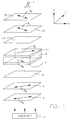
- Figure 1 is an exploded perspective view of the optical components of a normally white twisted nematic LCD according to an embodiment of this invention, the display including both a pair of negative retarders and a pair of positive retarders sandwiching a liquid crystal layer therebetween.
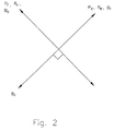
- Figure 2 illustrates the angular relationships between the respective optical axes of the Figure 1 components according to a first embodiment of this invention.
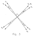
- Figure 3 illustrates the angular relationships between the respective optical axes of the components of the Figure 1 display according to a second embodiment of this invention, the second embodiment differing from the Figure 2 embodiment in that the axes of the positive retarders are angled about 3° with respect to their adjacent polarizer transmission axes.
- Figure 4 is a white light contrast ratio contour graph or plot of the Example 1 twisted nematic normally white liquid crystal light valve when 5.0 driving volts was applied thereto according to the Figure 1 - 2 embodiment of this invention.
- Figure 5 is a white light contrast ratio contour graph of the Figure 4 light valve when 7.0 driving volts was applied thereto.
- Figure 6 is a white light contrast ratio contour graph of the Example 2 6" x 8", AMLCD (normally white) according to the Figure 3 embodiment of this invention when ⁇ equals 3°, this Figure 6 graph illustrating the display when 6.1 driving volts was applied thereto.
- Figure 7 is a transmission (intensity) versus driving voltage graph of the Figure 6 normally white AMLCD, this graph showing the excellent gray level behavior of this display.
- Figure 8 is a white light contrast ratio contour graph of the Example 3 normally white light valve when 6 driving volts was applied thereto.
- Figure 9 is a white light contrast ratio contour graph of the Example 4 normally white light valve according to the Figures 1 - 2 embodiments when 6 driving volts was applied thereto.
- Figure 10 is a white light contrast ratio contour graph of the Example 5 normally white light valve according to when six driving volts was applied thereto.
- Figure 11 is a white light contrast ratio contour graph of the Example 6 normally white light valve when 6 driving volts was applied thereto.
- Figure 12 is a white light contrast ratio contour graph of the Example 12 normally white AMLCD similar to that shown in Figures 1 - 2 except that positive and negative retarders are provided on only one side of the liquid crystal layer, this display including one positive retarder (140 nm) and one negative retarder (-110 nm) on the same side of the LC layer.
- Figure 13 is a transmission versus driving voltage plot or graph of the Figure 12 AMLCD.
- FIG. 1 is an exploded schematic view of the optical components and their respective orientations of a twisted nematic NW LCD according to a first embodiment of this invention, the LCD being a light valve or an AMLCD having a matrix array of pixels and colored (i.e. RGB) subpixels in certain embodiments.
- this display includes from the rear forward toward viewer 1, conventional backlight 3, rear or light-entrance linear polarizer 5, rear positive uniaxial retardation film 2, rear negative retardation film 4, rear buffing or orientation film 7, liquid crystal layer 9, front buffing or orientation film 11, front negative retardation film 13, front positive uniaxial retardation film 14, and finally front or light-exit linear polarizer 15.
- Glass substrate (not shown) are located on either (i.e.
- Backlight 3 is conventional in nature and emits substantially collimated or alternatively diffused light toward the display panel.
- Backlight 3 may be, for example, the backlighting assembly disclosed in commonly owned U.S. Patent No. 5,161,041, the disclosure of which is hereby incorporated herein by reference.
- Other conventional high intensity substantially collimated backlight assemblies may alternatively be used.
- Rear and front polarizers 5 and 15 respectively are linear in nature in certain embodiments of this invention and their respective linear transmission axes P R and P F are orientated substantially perpendicular to one another so that the displays of the different embodiments are of the normally white (NW) type. Therefore, when a driving voltage (e.g. 0.1 V) below the threshold voltage V th is applied by electrodes (not shown) across liquid crystal layer 9, transmission axes P R and P F of polarizers 5 and 15 respectively are orientated such that the light emitted from backlight 3 proceeds through and is linearly polarized in direction P R by polarizer 5, is then twisted (e.g.
- a NW display or pixel to which a voltage less than V th is applied is said to be in the "off-state” and appears white (or colored if color filters are present) to the viewer.
- These polarizers are commercially available from, for example, Nitto Denko America, as #G1220DUN.
- a substantial driving voltage e.g. about 6 volts
- the light transmitted through rear polarizer 5 is not significantly twisted by LC layer 9 and thus is substantially blocked by front polarizer 15 due to the fact that the polarization direction of light reaching the interior surface of front polarizer 15 is substantially perpendicular (or otherwise non-aligned) to transmission axis P F thereby resulting in substantially no light reaching viewer 1 by way of the selected pixel(s) to which the substantial driving voltage is applied.
- the selected pixels driven in the matrix array appear darkened to viewer 1, these pixels said to be in the "on-state".
- the amount of light reaching viewer 1 is dictated by the voltage applied to LC layer 9 - the higher the driving voltage, the darker the selected driven pixel(s) appear.
- transmission axis P R of rear polarizer 5 and transmission axis P F of front polarizer 15 are oriented in a manner substantially perpendicular to one another as shown in Figures 1 - 3 so as to define a normally white twisted nematic cell.
- polarizers 5 and 15 may be oriented in other conventional manners which also allow the cell or display to be of the normally white type.
- Rear and front orientation or buffing films 7 and 11, respectively, are conventional and may be made of a substantially transparent polyimide.
- Rear orientation film 7 is conventionally buffed or oriented in direction B R as shown in Figures 1 - 3.
- front film 11 is conventionally buffed in direction B F .
- Buffing directions B R and B F are oriented substantially perpendicular to one another as shown in Figures 1 - 3 so as to allow the molecules of liquid crystal layer 9 when in the off or non-driven state to be twisted from about 80° to 100°, most preferably about 90°.
- the term "off-state” means that a voltage below the threshold voltage (V th ) is applied across LC layer 9.
- Liquid crystal layer 9 has a thickness "d" of from about 4.5 to 6.0 ⁇ m according to certain embodiments, preferably about 5.5 ⁇ m.
- Layer 9 has a birefringent value ⁇ n of from about 0.08 to 0.10, preferably from about 0.084 to 0.086.
- the voltage applied across LC layer 9 determines the degree of twisting of the liquid crystal molecules and thus dictates the polarization direction of light emitted from the front or viewer side of layer 9.
- the polarization direction of light reaching polarizer 15 dictates the amount of light permitted to pass therethrough via axis P F and reach viewer 1 in that the closer aligned transmission axis P F and the polarization direction of light reaching polarizer 15, the more light which is allowed to pass and reach viewer 1.
- the application of voltage > V th to layer 9 causes the LC molecule to substantially align vertically, the LC molecules never completely stand on end or become perfectly aligned in the vertical direction as is known in the art. This gives rise to the need for retardation (or birefringent) film(s).
- Positively birefringent uniaxial retardation films 2 and 14 with optical axes R R and R F respectively in this first embodiment are disposed on opposing sides of liquid crystal layer 9 thereby sandwiching layer 9 therebetween.
- Retardation films 2 and 14 in certain embodiments of this invention are positively birefringent and uniaxial in nature, such films being obtained from, for example, Nitto Corporation, Japan, or Nitto Denko America, Incorporated, New Brunswick, New Jersey as Model No. NRF-140 (140 nm retarder).
- Negative retarders 4 and 13 may be obtained from Rockwell or the University of Akron and are described in U.S. Patent Nos. 5,344,916 and 5,071,997, both of which are hereby incorporated herein by reference.
- the positive and negative retarders, and the polarizers may be separate sheets, although they may be integrally formed or laminated together in other embodiments.
- films 2 and 4 for example, may be laminated together to form a single film having a positive retarding section and a negative retarding section.
- transmission axis P R , optical axis R R , and buffing direction B F are substantially parallel to one another in certain embodiments of this invention while rear buffing direction B R , front polarizer transmission axis P F , and optical axis R F are also substantially parallel to one another thereby causing the display to output substantially symmetrical viewing characteristics relative to the "normal" viewing angle.
- axis P R and direction B R are substantially perpendicular to one another as are axis P F and direction B F .
- a display having such an optical arrangement is said to be "X-buffed".
- the term "X-buffed" means that rear polarizer transmission axis P R is substantially perpendicular to rear buffing direction B R while front polarizer transmission axis P F is substantially perpendicular to front buffing direction B F .
- Figure 2 optical embodiment of the Figure 1 display illustrates front positive retarder optical axis R F being substantially parallel to front transmission axis P F and rear positive retarder axis R R being substantially parallel to rear polarizer transmission axis P R
- the positive retarder optical axes of retarders 2 and 14 may be angled from these positions as shown in the Figure 3 embodiment.
- Figure 3 illustrates an optical axis and directional configuration according to another (or second) embodiment of this invention corresponding to the Figure 1 display. As shown in Figure 3, ⁇ equals 3°.
- front positive retarder optical axis R F of retarder 14 is rotated 3° from axis P F in the counterclockwise direction (as viewed from the viewpoint of viewer 1), while rear positive retarder optical axis R R of retarder 2 is rotated 3° in the clockwise direction relative to rear polarizer transmission axis P R .
- ⁇ equals 3° the viewing zone of best contrast output by the display is shiftable in the vertical direction.
- This is of particular interest, for example, in avionic cockpit applications when the display's best viewing zone is needed, not at normal, but at a vertical viewing angle with respect thereto (e.g. an angle +20° vertical of normal).
- the retarder axes (R R and R F ) so that ⁇ equals 3° as shown in Figure 3, the viewing zone of highest contrast is shifted in the positive vertical direction with respect to normal (e.g. see Figure 6).
- the optical axes R R and R F of positive retarders 2 and 14 may be angled either symmetrically or non-symmetrically with respect to one another according to certain embodiments of this invention, depending on the desired viewing characteristics of the display.
- ⁇ for each positive retarder optical axis may be adjusted (in the same direction), for example, from about 0° to 8° in either the positive or negative direction. More preferably, ⁇ may be adjusted plus or minus about 3° to 8°, and most preferably about 3° to 5° in either direction.
- ⁇ for both (or alternatively only one) of the positive retarders as shown in Figure 3, the position of the highest contrast viewing zone may be shifted vertically and the highest contrast areas (i.e. the "eyes") in the viewing zone may be spaced closer or further apart (this is particularly useful when not only the pilot, but also the co-pilot must view a display within a cockpit).
- the retardation value of positive films 2 and 14 is from about 80 to 200 nm, more preferably from about 120 to 160 nm, and most preferably about 140 nm.
- both rear positive retarder 2 and front positive retarder 14 have retardation values of 140 nm while both rear negative retarder 4 and front negative retarder 13 each have a retardation value of -110 nm.
- the ratio of the positive retardation value of each of positive retarders 2 and 14 to the negative retardation value of negative retarders 4 and 13 is from about 1:1 to 2:1. More preferably, the retardation value ratio for the positive retarders to the negative retarders is from about 1.2:1 to 1.5:1.
- the retardation values of each of the like (e.g. positive) retarders need not be identical, so long as the ratio range is met by both sets of positive:negative retardation values.
- the improved viewing characteristics resulting from maintaining the positive and negative retarder values within these ratios will be illustrated below with respect to Figures 4 - 13 and the numerous examples herein.
- a normally white twisted nematic X-buffed light valve was made as shown in Figures 1 - 2.
- Liquid crystal layer 9 had a thickness of about 5.5 ⁇ m and a ⁇ n value of about 0.084. Liquid crystal layer 9 twisted normally incident light about 90° when in the off-state.
- Positive uniaxial retarders 2 and 14 of this light valve each had a positive retardation value of 140 nm while negative retarders 4 and 13 each had a retardation value of -110 nm.
- the negative retarders 4 and 13 were located interior of the two positive retarders 2 and 14 as shown in Figure 1.
- optical axes were arranged as shown in Figure 2 ("X-buffed") so that the front and rear polarizer transmission axes were substantially perpendicular to one another while P F was substantially parallel to R F and B R .
- Front buffing direction B F was substantially parallel to P R and R R of polarizer 5 and positive uniaxial retarder 2 respectively.
- the optical axis of each negative retarder was substantially perpendicular to the plane of the retarder.
- the positive to negative retardation value of ratio on each side of LC layer 9 was 1.27 in this Example.
- Figures 4 and 5 are white light contrast ratio graphs of the light valve made in this Example when 5.0 and 7.0 volts, respectively, were applied across LC layer 9.
- LC layer 9 was substantially at room temperature or slightly higher (e.g. about 38° - 40°C).
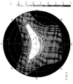
- Figure 4 when 5.0 driving volts was applied to the light valve, excellent contrast ratios were achieved over a wide range of viewing angles, the 80:1 or 80 contour line extending horizontally at least about ⁇ 40°.
- Figure 5 when 7.0 driving volts was applied to the light valve, the 80:1 and greater contrast ratio viewing zone expanded vertically and slightly contracted horizontally.
- the 80:1 or 80 contrast ratio viewing zone extended horizontally along the 0° vertical viewing axis to about ⁇ 37° to 38°.
- the 10:1 contrast ratio viewing zone extended horizontally along the 0° vertical viewing axis across the entire graph and vertically along the 0° horizontal viewing axis to about +45° and -35°.
- the viewing characteristics illustrated in Figures 4 - 5 for this light valve are superior to the prior art as a result of the retardation values provided for the positive and negative retarders and their locations in the display stack.
- a 6" x 8" TFT driven X-buffed active matrix liquid crystal display (AMLCD) as shown in Figures 1 and 3 with RGB color filters was made and analyzed in this Example.
- the AMLCD of this Example had a substantially common TN liquid crystal material 9 thickness of about 5.2 ⁇ m across the entire display panel.
- Liquid crystal layer 9 had a ⁇ n of about 0.084.
- the positive to negative retardation value ratio was 1.27 on both sides of layer 9.
- front polarizer transmission axis P F was substantially parallel to rear buffing direction B R , these directions being angled about 3° from front positive retarder optical axis R F as shown in Figure 3.
- rear polarizer transmission axis P R was substantially perpendicular to front transmission axis P F , with rear transmission axis P R being substantially parallel to front buffing direction B F and angled about 3° from R R as shown in Figure 3.
- Figure 6 is a white light contrast ratio graph of the AMLCD of this Example when 6.1 volts was applied thereto.
- the high contrast viewing region was shifted vertically upward due to the adjustment of ⁇ to a value of 3° on each side of LC layer 9.
- the 90 to 100 contrast ratio area extended horizontally along the +10° vertical axis from about -40° to +48°, this being a marked improvement over the prior art.
- the two high contrast (eye) regions in the center of the high contrast area define contrast ratios up to and including about 240:1 or 240.
- These two “eyes” can be made into one or alternatively spaced further apart by increasing and decreasing ⁇ (move retarder axis or axes) and/or rotating the polarizer axes by themselves symmetrically (symmetrically on both sides of LC layer 9).
- Figure 7 is a transmission (intensity) versus driving voltage graph for the AMLCD of this Example.
- the Figure 7 graph illustrates the lack of inversion and superior gray level behavior of this TFT driven display.
- a normally white twisted nematic X-buffed light valve was made and analyzed (see Figure 8).
- This light valve was made up as shown in Figures 1 - 2 so that ⁇ equalled 0° on both sides of LC layer 9.
- Liquid crystal layer 9 had a thickness of about 5.5 ⁇ m.
- Positive retardation films 2 and 14 each had a positive retardation value of 300 nm.
- Negative retarders 4 and 13 each had a retardation value of -220 nm.
- both a positive and negative retarder was positioned on each side of liquid crystal layer 9, with the negative retarder on each side being sandwiched between the adjacent positive retarder and the liquid crystal layer.
- the positive to negative retardation value ratio was 1.364 on each side of the panel for this Example.
- Figure 8 is a white light contrast ratio graph of the light valve of this Example when about 6 volts was applied thereto.
- the above 80:1 contrast ratio area i.e. the white area in the center of the graph
- the above 30:1 contrast ratio viewing zone extended horizontally along the 0° vertical viewing axis from about -40° to +40°.
- the positive to negative retardation value ratio for this Example was 1.364 on each side of the light valve.
- a normally white twisted nematic light valve was manufactured and analyzed as shown in Figure 9.
- liquid crystal layer 9 twisted normally incident light about 90° when in the off-state.
- This X-buffed light valve was made up as shown in Figures 1 - 2.
- Liquid crystal layer 9 had a thickness of about 5.5 ⁇ m.
- Positive retarders 2 and 14 each had a retardation value of 430 nm.
- Negative retarders 4 and 13 each had a retardation value of -220 nm.
- the positive to negative retardation value ratio for this Example was 1.95 on each side of layer 9. ⁇ was 0°.
- Figure 9 is a white light contrast ratio graph showing the output to viewer 1 of the light valve of this Example when about 6 volts was applied thereto. While the output as shown in Figure 9 was not quite as symmetrical as that of the previous Example (see Figure 8), it still produced satisfactory results. The acceptable contrast ratio area extended well into the positive vertical region, however, the negative vertical region contrast ratios were less than desirable depending upon the application in which the light valve is to be used.
- the light valve manufactured and analyzed in this Example is used as a comparison to the previous Examples for the purpose of illustrating the characteristics of an unacceptable contrast ratio output.
- Liquid crystal layer 9 provided about a 90° twist and was about 5.5 ⁇ m thick.
- Positive retarders 2 and 14 on either side of layer 9 each had a retardation value of 430 nm while negative retarders 4 and 13 each had a retardation value of 110 nm.
- the positive to negative retardation value ratio in this Example was 3.91 on each side of LC layer 9.
- Figure 10 is a white light contrast ratio graph of the output of this light valve when about 6 volts was applied thereto.
- Figure 10 is a white light contrast ratio graph of the output of this light valve when about 6 volts was applied thereto.
- the light valve manufactured in this Example output less than desirable viewing characteristics when about 6 volts was applied thereto.
- the above 80:1 contrast ratio viewing area is much smaller than in the previous Examples as are many of the other defined contrast ratio regions.
- the output of this light valve given the rather high positive/negative retardation value ratio of 3.91 is less than desirable.
- the light valve manufactured and analyzed in this Example is generally undesirable.
- This light valve was manufactured as shown in Figures 1 - 2 so that ⁇ equalled 0°.
- Liquid crystal layer 9 was 5.5 ⁇ m thick.
- this light valve was "X-buffed".
- Positive uniaxial retarders 2 and 14 of this light valve each had a retardation value of 140 nm, while negative retarders 4 and 13 each had a retardation value of -220 nm.
- this normally white twisted nematic light valve had an LC layer 9 which twisted normally incident light about 90° when in the off-state.
- Figure 11 is a white light contrast ratio graph of the output of this light valve when about 6.0 volts was applied thereto. By comparing the output of this light valve with those of the previous Examples, it can be seen that the Figure 11 viewing characteristics are less than desirable and non-symmetric in view of the rather low positive/negative retardation value ratio of 0.64 on both sides of LC layer 9 in this Example.
- this AMLCD is illustrated by the optical components shown in Figure 1 simply by removing rear films 2 and 4.
- the sole negative retardation film 13 having a birefringent value of -110 nm was located between liquid crystal layer 9 and the sole positive retardation film 14 which had a retardation value of 140 nm.
- the positive to negative retardation value ratio was about 1.27 on the front side of LC layer 9.
- Figure 12 is a white light contrast ratio graph of the normally white twisted nematic AMLCD of this Example when about 7 volts was applied thereto.
- the high contrast viewing zone has been shifted vertically upward relative to the previously satisfactory Examples because positive and negative retarders were utilized on only one side of LC layer 9.
- Such a display output may be advantageous in certain applications such as cockpit applications where the display is positioned below the pilot's line of view.
- Figure 13 is a transmission versus driving voltage plot at horizontal viewing angles along the 0° vertical viewing axis of the AMLCD of this Example illustrating the lack of inversion humps and superior and improved gray level behavior of this display. This concludes all Examples herein.
Abstract
Description
- This application is a continuation-in-part (CIP) of Serial No. 08/167,652, filed December 15, 1993.
- This invention relates to a normally white (NW) liquid crystal display (LCD) including positive and negative retardation films. More particularly, this invention relates to a NW twisted nematic LCD including positive and negative retardation films (birefringent films) of specific values and/or within a specific ratio range.
- This application relates to commonly owned U.S. Serial Nos. 08/167,652, filed December 15, 1993, 08/255,971, filed June 8, 1994, and 08/235,691, filed April 29, 1994, the disclosures of which are hereby incorporated herein by reference. Each of these copending commonly owned applications relates to a liquid crystal display with specific retarder values and/or positions.
- Informational data in typical liquid crystal displays (LCDs) is presented in the form of a matrix array of rows and columns of numerals or characters (i.e. pixels) which are generated by a number of segmented electrodes arranged in a matrix pattern. The segments are connected by individual leads to driving electronics which apply a voltage to the appropriate combination of segments and adjacent LC material in order to display the desired data and/or information by controlling the light transmitted through the liquid crystal material.
- Contrast ratio is one of the most important attributes considered in determining the quality of both normally white (NW) and normally black (NB) liquid crystal displays. The contrast ratio in a normally white display is determined in low ambient conditions by dividing the "off-state" light transmission (high intensity white light) by the "on-state" or darkened transmitted intensity. For example, if the "off-state" transmission is 200 fL at a particular viewing angle and the "on-state" transmission is 5 fL at the same viewing angle, then the display's contrast ratio at that particular viewing angle is 40 or 40:1 for the particular "on-state" driving voltage utilized.
- Accordingly, in normally white LCDs a significant factor adversely limiting the contrast ratio is the amount of light which leaks through the display in the darkened or "on-state." In a similar manner, in normally black displays, a significant factor limiting the contrast ratio achievable is the amount of light which leaks through the display in the darkened or "off-state." The higher and more uniform the contrast ratio of a particular display over a wide range of viewing angles, the better the LCD in most applications.
- Normally black (NB) twisted nematic displays typically have better contrast ratio contour curves or characteristics then do their counterpart NW displays (i.e. the NB image can be seen better at large viewing angles). However, NB displays are much harder to manufacture than NW displays due to their high dependence on the cell gap or thickness "d" of the liquid crystal layer as well as on the temperature of the liquid crystal material itself. Accordingly, a long-felt need in the art has been the ability to construct a normally white display with high contrast ratios over a large range of viewing angles, rather than having to resort to the more difficult to manufacture NB displays to achieve these characteristics.
- What is generally needed in NW displays is an optical compensating or retarding element(s), i.e. retardation film, which introduces a phase delay that restores the original polarization state of the light, thus allowing the light to be substantially blocked by the output polarizer in the "on-state." Optical compensating elements or retarders are known in the art and are disclosed, for example, in U.S. Patent Nos. 5,184,236; 5,189,538; 5,406,396; 4,889,412; 5,344,916; 5,196,953; 5,138,474; and 5,071,997.
- The disclosures of 08/255,971 and 08/167,652 (both incorporated herein by reference) in their respective "Background" sections illustrate and discuss contrast ratios and driving voltage versus intensity (fL) graphs of prior art NW displays, which are less than desirable. Prior art NW LCD viewing characteristics are problematic in that, for example, their contrast ratios are limited both horizontally and vertically (and often non-symmetric), and their gray level performance lacks consistency.
- Gray level performance and the corresponding amount of inversion are also important in determining the quality of an LCD. Conventional active matrix liquid crystal displays typically utilize anywhere from about 8 to 64 different driving voltages. These different driving voltages are generally referred to as "gray level" voltages. The intensity of light transmitted through the pixel(s) or display depends upon the driving voltage utilized. Accordingly, conventional gray level voltages are used to generate dissimilar shades of color so as to create different colors when, for example, the shades are mixed with one another.
- Preferably, the higher the driving voltage in a normally white display, the lower the intensity (fL) of light transmitted therethrough. The opposite is true in normally black displays. Thus, by utilizing multiple gray level driving voltages, one can manipulate either a NW or NB liquid crystal display to emit desired intensities and shades of light/color. A gray level VON is generally known as any driving voltage greater than Vth (threshold voltage) up to about 5 to 6.5 volts.
- Gray level intensity in an LCD is dependent upon the display's driving voltage. It is desirable in NW displays to have an intensity versus driving voltage curve wherein the intensity of light emitted from the display or pixel continually and monotonically decreases as the driving voltage increases. In other words, it is desirable to have gray level performance in a NW pixel such that the intensity (fL) at 6.0 volts is less than that at 5.0 volts, which is in turn less than that at 4.0 volts, which is less than that at 3.0 volts, which is in turn less than that at 2.0 volts, etc. Such desired gray level curves across a wide range of view allows the intensity of light reaching viewers at different viewing angles to be easily and consistently controlled.
- Serial Nos. 08/255,971 and 08/167,652 discuss, in their respective "Background" sections, prior art NW LCDs with inversion problems (e.g. inversion humps, specifically their transmission versus driving voltage graphs). As discussed therein, inversion humps are generally undesirable. A theoretically perfect driving voltage versus intensity (fL) curve for an NW display would have a decreased intensity (fL) for each increase in gray level driving voltage at all viewing angles. In contrast to this, inversion humps represent increase(s) in intensity of radiation emitted from the LCD or light valve for each corresponding increase in gray level driving voltage. Accordingly, it would satisfy a long-felt need in the art if a normally white TN liquid crystal display could be provided with no or little inversion and improved contrast ratios over a wide range of viewing angles.
- U.S. Patent No. 5,344,916 discloses a liquid crystal display including retardation films having positive and negative retardation films. The negative retarders (or birefringent films) of the '916 patent have as a characteristic that

- Unfortunately, while use of the negative retardation films of the '916 patent improves contrast over some prior art LCDs, twisted nematic (TN) displays including same often still suffer from less than desirable contrast ratios at large viewing angles. Pointedly, the disclosure of the '916 patent does not appreciate, suggest, or disclose the use of negative and positive retarders together at specified values, ratios, and/or locations to even further improve viewing characteristics of an LCD as discussed below by the instant inventors.
- U.S. Patent No. 5,189,538 (and 5,138,747) discloses a super twisted nematic (STN) LCD including films having different birefringent values. Unfortunately, STN LCDs have no real correspondence or correlation to ≈90° TN LCDs with regard to the behavior of the image due to retarders. In other words, teachings regarding retarders in STN devices (e.g. 270° twist) generally little or have no relevance with regard to TN (≈90° twist) LCDs.
- U.S. Patent No. 4,889,412 discloses a LCD with electrically controlled birefringence (ECB) and negative anisotropy. Unfortunately, ECB displays do not use twisted nematic LC material as does the instant invention. Again, ECB display teachings are generally unrelated to TN (≈90° twist) displays with regard to retardation teachings and principles.
- U.S. Patent No. 5,291,323 discloses a liquid crystal display with "positive and negative compensating films each with its optical axis parallel to the surface." Unfortunately, the disclosure and teaching of the '323 patent are unrelated to TN displays such as those of the instant invention in that the '323 patent relates to supertwisted (e.g. 240° twist) LCDs. It is also worth noting that the slow phase axis directions of certain phase plates in the '323 patent are parallel to the surface (i.e. plane defined by the layer).
- The term "rear" when used herein but only as it is used to describe substrates, polarizers, electrodes, buffing zones, and orientation films means that the described element is on the backlight side of the liquid crystal material, or in other words, on the side of the LC material opposite the viewer.
- The term "front" when used herein but only as it is used to describe substrates, polarizers, electrodes, buffing zones and orientation films means that the described element is located on the viewer side of the liquid crystal material.
- The LCDs and light valves herein include a liquid crystal material with a birefringence (Δn) of 0.084 at room temperature, Model No. ZLI-4718 obtained from Merck, unless specified otherwise.
- The term "retardation value" as used herein means "d · Δn" of the retardation film or plate, wherein "d" is the film thickness and "Δn" is the film birefringence.
- The term "interior" when used herein to describe a surface or side of elements (or an element itself), means closest to the liquid crystal material.
- The term "light valve" as used herein means a liquid crystal display including a rear linear polarizer, a rear transparent substrate, a rear continuous pixel electrode, a rear orientation film, an LC layer, a front orientation film, a front continuous pixel electrode, a front substrate, and a front polarizer (without the presence of color filters and driving active matrix circuitry such as TFTs). Such a light valve may also include a retardation film(s) disposed on either side of the LC layer as described with respect to each example and embodiment herein. In other words, a "light valve" may be referred to as one giant pixel without segmented electrodes.
- It is apparent from the above that there exists a need in the art for a normally white liquid crystal display wherein the viewing zone of the display has both high contrast ratios and little or no inversion over a wide range of viewing angles.
- This invention will now be described with respect to certain embodiments thereof, accompanied by certain illustrations wherein:
- Generally speaking this invention fulfills the above-described needs in the art by providing a normally white twisted nematic liquid crystal display comprising:
- a liquid crystal layer for twisting at least one normally incident visible wavelength of light from about 80° to 100° as it passes therethrough when the liquid crystal layer is in substantially the off-state thereby defining a twisted nematic display;
- a pair of negative retarders sandwiching the liquid crytal layer therebetween;
- a pair of positive retarders sandwiching both the liquid crystal layer and the negative retarders therebetween; and
- According to certain other embodiments of this invention, a method of making a twisted nematic LCD is provided comprising the steps of:
- providing a pair of negative retarders defined by

- providing a pair of positive unaxial retarders;
- disposing a twisted nematic liquid crystal layer between a pair of negative retarders and between the pair of positive retarders; and
- disposing the pair of negative retarders between the pair of positive retarders so that the resulting display output contrast ratios of at least about 20 at horizontal viewing angles along the 0° vertical axis of about ±40°.
- This invention will now be described with respect to certain embodiments thereof, along with reference to the accompanying illustrations, wherein:
- Figure 1 is an exploded perspective view of the optical components of a normally white twisted nematic LCD according to an embodiment of this invention, the display including both a pair of negative retarders and a pair of positive retarders sandwiching a liquid crystal layer therebetween.
- Figure 2 illustrates the angular relationships between the respective optical axes of the Figure 1 components according to a first embodiment of this invention.
- Figure 3 illustrates the angular relationships between the respective optical axes of the components of the Figure 1 display according to a second embodiment of this invention, the second embodiment differing from the Figure 2 embodiment in that the axes of the positive retarders are angled about 3° with respect to their adjacent polarizer transmission axes.
- Figure 4 is a white light contrast ratio contour graph or plot of the Example 1 twisted nematic normally white liquid crystal light valve when 5.0 driving volts was applied thereto according to the Figure 1 - 2 embodiment of this invention.
- Figure 5 is a white light contrast ratio contour graph of the Figure 4 light valve when 7.0 driving volts was applied thereto.
- Figure 6 is a white light contrast ratio contour graph of the Example 2 6" x 8", AMLCD (normally white) according to the Figure 3 embodiment of this invention when φ equals 3°, this Figure 6 graph illustrating the display when 6.1 driving volts was applied thereto.
- Figure 7 is a transmission (intensity) versus driving voltage graph of the Figure 6 normally white AMLCD, this graph showing the excellent gray level behavior of this display.
- Figure 8 is a white light contrast ratio contour graph of the Example 3 normally white light valve when 6 driving volts was applied thereto.
- Figure 9 is a white light contrast ratio contour graph of the Example 4 normally white light valve according to the Figures 1 - 2 embodiments when 6 driving volts was applied thereto.
- Figure 10 is a white light contrast ratio contour graph of the Example 5 normally white light valve according to when six driving volts was applied thereto.
- Figure 11 is a white light contrast ratio contour graph of the Example 6 normally white light valve when 6 driving volts was applied thereto.
- Figure 12 is a white light contrast ratio contour graph of the Example 12 normally white AMLCD similar to that shown in Figures 1 - 2 except that positive and negative retarders are provided on only one side of the liquid crystal layer, this display including one positive retarder (140 nm) and one negative retarder (-110 nm) on the same side of the LC layer.
- Figure 13 is a transmission versus driving voltage plot or graph of the Figure 12 AMLCD.
- Figure 1 is an exploded schematic view of the optical components and their respective orientations of a twisted nematic NW LCD according to a first embodiment of this invention, the LCD being a light valve or an AMLCD having a matrix array of pixels and colored (i.e. RGB) subpixels in certain embodiments. As shown, this display includes from the rear forward toward
viewer 1,conventional backlight 3, rear or light-entrancelinear polarizer 5, rear positiveuniaxial retardation film 2, rearnegative retardation film 4, rear buffing ororientation film 7,liquid crystal layer 9, front buffing ororientation film 11, frontnegative retardation film 13, front positiveuniaxial retardation film 14, and finally front or light-exitlinear polarizer 15. Glass substrate (not shown) are located on either (i.e. both) side oflayer 9 so as to be disposed between the respective orientation films and their adjacent negative retarders. Electrodes (not shown) are disposed between the substrates and their adjacent orientation layers. The key to this invention is the surprise finding that when the positive and negative retarders listed above are each within a particular retardation value(s) range and/or ratio, improved viewing characteristics of the display result. -
Backlight 3 is conventional in nature and emits substantially collimated or alternatively diffused light toward the display panel.Backlight 3 may be, for example, the backlighting assembly disclosed in commonly owned U.S. Patent No. 5,161,041, the disclosure of which is hereby incorporated herein by reference. Other conventional high intensity substantially collimated backlight assemblies may alternatively be used. - Rear and
front polarizers liquid crystal layer 9, transmission axes PR and PF ofpolarizers backlight 3 proceeds through and is linearly polarized in direction PR bypolarizer 5, is then twisted (e.g. from about 80° to 100°) by twistednematic LC layer 9, and finally exitsfront polarizer 15 via transmission axis PF thus reachingviewer 1. The light reachesviewer 1 because its polarization direction upon reachingfront polarizer 15 is similar to the direction defined by transmission axis PF. Thus, a NW display or pixel to which a voltage less than Vth is applied is said to be in the "off-state" and appears white (or colored if color filters are present) to the viewer. These polarizers are commercially available from, for example, Nitto Denko America, as #G1220DUN. - However, when a substantial driving voltage (e.g. about 6 volts) is applied across selected NW pixels of the matrix array including
liquid crystal layer 9, the light transmitted throughrear polarizer 5 is not significantly twisted byLC layer 9 and thus is substantially blocked byfront polarizer 15 due to the fact that the polarization direction of light reaching the interior surface offront polarizer 15 is substantially perpendicular (or otherwise non-aligned) to transmission axis PF thereby resulting in substantially nolight reaching viewer 1 by way of the selected pixel(s) to which the substantial driving voltage is applied. Thus, the selected pixels driven in the matrix array appear darkened toviewer 1, these pixels said to be in the "on-state". As will be appreciated by those of skill in the art, the amount of light reachingviewer 1 is dictated by the voltage applied to LC layer 9 - the higher the driving voltage, the darker the selected driven pixel(s) appear. - In certain embodiments of this invention, transmission axis PR of
rear polarizer 5 and transmission axis PF offront polarizer 15 are oriented in a manner substantially perpendicular to one another as shown in Figures 1 - 3 so as to define a normally white twisted nematic cell. However,polarizers - Rear and front orientation or buffing
films Rear orientation film 7 is conventionally buffed or oriented in direction BR as shown in Figures 1 - 3. Likewise,front film 11 is conventionally buffed in direction BF. Buffing directions BR and BF are oriented substantially perpendicular to one another as shown in Figures 1 - 3 so as to allow the molecules ofliquid crystal layer 9 when in the off or non-driven state to be twisted from about 80° to 100°, most preferably about 90°. The term "off-state" means that a voltage below the threshold voltage (Vth) is applied acrossLC layer 9. -
Liquid crystal layer 9 has a thickness "d" of from about 4.5 to 6.0 µm according to certain embodiments, preferably about 5.5 µm.Layer 9 has a birefringent value Δn of from about 0.08 to 0.10, preferably from about 0.084 to 0.086. - The voltage applied across
LC layer 9 determines the degree of twisting of the liquid crystal molecules and thus dictates the polarization direction of light emitted from the front or viewer side oflayer 9. In turn, the polarization direction of light reachingpolarizer 15 dictates the amount of light permitted to pass therethrough via axis PF and reachviewer 1 in that the closer aligned transmission axis PF and the polarization direction of light reachingpolarizer 15, the more light which is allowed to pass and reachviewer 1. While the application of voltage > Vth to layer 9 causes the LC molecule to substantially align vertically, the LC molecules never completely stand on end or become perfectly aligned in the vertical direction as is known in the art. This gives rise to the need for retardation (or birefringent) film(s). - Positively birefringent
uniaxial retardation films liquid crystal layer 9 thereby sandwichinglayer 9 therebetween. Surprisingly, it has been found that the provision of the above-listed four retardation films (two positive and two negative) of particular retardation values and/or ratios reduces inversion and improves viewing zone contrast ratios at over a large range of viewing angles. -
Retardation films -
Negative retarders 
Negative retarders films - With reference to Figure 2, transmission axis PR, optical axis RR, and buffing direction BF are substantially parallel to one another in certain embodiments of this invention while rear buffing direction BR, front polarizer transmission axis PF, and optical axis RF are also substantially parallel to one another thereby causing the display to output substantially symmetrical viewing characteristics relative to the "normal" viewing angle. In such embodiments, axis PR and direction BR are substantially perpendicular to one another as are axis PF and direction BF. A display having such an optical arrangement is said to be "X-buffed". The term "X-buffed" means that rear polarizer transmission axis PR is substantially perpendicular to rear buffing direction BR while front polarizer transmission axis PF is substantially perpendicular to front buffing direction BF.
- While the Figure 2 optical embodiment of the Figure 1 display illustrates front positive retarder optical axis RF being substantially parallel to front transmission axis PF and rear positive retarder axis RR being substantially parallel to rear polarizer transmission axis PR, the positive retarder optical axes of
retarders retarder 14 is rotated 3° from axis PF in the counterclockwise direction (as viewed from the viewpoint of viewer 1), while rear positive retarder optical axis RR ofretarder 2 is rotated 3° in the clockwise direction relative to rear polarizer transmission axis PR. By angling the positive retardation axes ofretarders - The optical axes RR and RF of
positive retarders - It has been found that by providing the positive and negative retarders of this invention with particular retardation or birefringent values and/or ratios, improved viewing characteristics (higher contrast ratios and/or less inversion) of a normally white twisted nematic display are achieved. According to certain embodiments of this invention, the retardation value of
positive films negative retardation films positive retarder 2 and frontpositive retarder 14 have retardation values of 140 nm while both rearnegative retarder 4 and frontnegative retarder 13 each have a retardation value of -110 nm. - According to certain other embodiments, it has been found that improved viewing characteristics result when the retardation values of the positive and negative retarders are maintained within a particular ratio range. The ratio of the positive retardation value of each of
positive retarders negative retarders - This invention will now be described with respect to certain examples as follows:
- In this first Example, a normally white twisted nematic X-buffed light valve was made as shown in Figures 1 - 2.
Liquid crystal layer 9 had a thickness of about 5.5 µm and a Δn value of about 0.084.Liquid crystal layer 9 twisted normally incident light about 90° when in the off-state. Positiveuniaxial retarders negative retarders negative retarders positive retarders polarizer 5 and positiveuniaxial retarder 2 respectively. The indices of refraction ofnegative retarders 
LC layer 9 was 1.27 in this Example. - Figures 4 and 5 are white light contrast ratio graphs of the light valve made in this Example when 5.0 and 7.0 volts, respectively, were applied across
LC layer 9. As in all Examples herein,LC layer 9 was substantially at room temperature or slightly higher (e.g. about 38° - 40°C). As shown in Figure 4 when 5.0 driving volts was applied to the light valve, excellent contrast ratios were achieved over a wide range of viewing angles, the 80:1 or 80 contour line extending horizontally at least about ±40°. Then, in Figure 5, when 7.0 driving volts was applied to the light valve, the 80:1 and greater contrast ratio viewing zone expanded vertically and slightly contracted horizontally. As can be seen in Figure 5, the 80:1 or 80 contrast ratio viewing zone extended horizontally along the 0° vertical viewing axis to about ±37° to 38°. Likewise, the 10:1 contrast ratio viewing zone extended horizontally along the 0° vertical viewing axis across the entire graph and vertically along the 0° horizontal viewing axis to about +45° and -35°. The viewing characteristics illustrated in Figures 4 - 5 for this light valve are superior to the prior art as a result of the retardation values provided for the positive and negative retarders and their locations in the display stack. - A 6" x 8" TFT driven X-buffed active matrix liquid crystal display (AMLCD) as shown in Figures 1 and 3 with RGB color filters was made and analyzed in this Example. The AMLCD of this Example had a substantially common TN
liquid crystal material 9 thickness of about 5.2 µm across the entire display panel.Liquid crystal layer 9 had a Δn of about 0.084.Positive retardation films LC layer 9 therebetween in this Example (as in the other Examples herein) each had a retardation value of 140 nm whilenegative retardation films layer 9 each had a retardation value of -110 nm. Thus, the positive to negative retardation value ratio was 1.27 on both sides oflayer 9. The optical axes and directions of this AMLCD were provided as shown in Figure 3 so that φ equalled positive 3°. Thus, front polarizer transmission axis PF was substantially parallel to rear buffing direction BR, these directions being angled about 3° from front positive retarder optical axis RF as shown in Figure 3. Likewise, rear polarizer transmission axis PR was substantially perpendicular to front transmission axis PF, with rear transmission axis PR being substantially parallel to front buffing direction BF and angled about 3° from RR as shown in Figure 3. - Figure 6 is a white light contrast ratio graph of the AMLCD of this Example when 6.1 volts was applied thereto. As can be seen in Figure 6, the high contrast viewing region was shifted vertically upward due to the adjustment of φ to a value of 3° on each side of
LC layer 9. The 90 to 100 contrast ratio area extended horizontally along the +10° vertical axis from about -40° to +48°, this being a marked improvement over the prior art. Additionally, the two high contrast (eye) regions in the center of the high contrast area define contrast ratios up to and including about 240:1 or 240. These two "eyes" can be made into one or alternatively spaced further apart by increasing and decreasing φ (move retarder axis or axes) and/or rotating the polarizer axes by themselves symmetrically (symmetrically on both sides of LC layer 9). - Figure 7 is a transmission (intensity) versus driving voltage graph for the AMLCD of this Example. The Figure 7 graph illustrates the lack of inversion and superior gray level behavior of this TFT driven display.
- In this Example, a normally white twisted nematic X-buffed light valve was made and analyzed (see Figure 8). This light valve was made up as shown in Figures 1 - 2 so that φ equalled 0° on both sides of
LC layer 9.Liquid crystal layer 9 had a thickness of about 5.5 µm.Positive retardation films Negative retarders liquid crystal layer 9, with the negative retarder on each side being sandwiched between the adjacent positive retarder and the liquid crystal layer. The positive to negative retardation value ratio was 1.364 on each side of the panel for this Example. - Figure 8 is a white light contrast ratio graph of the light valve of this Example when about 6 volts was applied thereto. As can be seen, the above 80:1 contrast ratio area (i.e. the white area in the center of the graph) extended horizontally along the 0° vertical axis from about -30° to +26°. Likewise, the above 30:1 contrast ratio viewing zone extended horizontally along the 0° vertical viewing axis from about -40° to +40°. These are significant improvements over the prior art. The contrast ratios output by this light valve are also expanded in the vertical direction relative to certain prior art displays. Because the
positive retarders negative retarders - In this Example, a normally white twisted nematic light valve was manufactured and analyzed as shown in Figure 9. As in each of the Examples herein,
liquid crystal layer 9 twisted normally incident light about 90° when in the off-state. This X-buffed light valve was made up as shown in Figures 1 - 2.Liquid crystal layer 9 had a thickness of about 5.5 µm.Positive retarders Negative retarders layer 9. φ was 0°. - Figure 9 is a white light contrast ratio graph showing the output to
viewer 1 of the light valve of this Example when about 6 volts was applied thereto. While the output as shown in Figure 9 was not quite as symmetrical as that of the previous Example (see Figure 8), it still produced satisfactory results. The acceptable contrast ratio area extended well into the positive vertical region, however, the negative vertical region contrast ratios were less than desirable depending upon the application in which the light valve is to be used. - The light valve manufactured and analyzed in this Example is used as a comparison to the previous Examples for the purpose of illustrating the characteristics of an unacceptable contrast ratio output. The X-buffed light valve according to this Example was made as shown in Figures 1 - 2 (φ = 0°).
Liquid crystal layer 9 provided about a 90° twist and was about 5.5 µm thick.Positive retarders layer 9 each had a retardation value of 430 nm whilenegative retarders LC layer 9. - Figure 10 is a white light contrast ratio graph of the output of this light valve when about 6 volts was applied thereto. By comparing the Figure 10 graph to the graphs of Figures 4 - 8, it can be seen that the light valve manufactured in this Example output less than desirable viewing characteristics when about 6 volts was applied thereto. For example, the above 80:1 contrast ratio viewing area is much smaller than in the previous Examples as are many of the other defined contrast ratio regions. In accordance with the spirit of this invention, the output of this light valve given the rather high positive/negative retardation value ratio of 3.91 is less than desirable.
- As with the previous Example, the light valve manufactured and analyzed in this Example is generally undesirable. This light valve was manufactured as shown in Figures 1 - 2 so that φ equalled 0°.
Liquid crystal layer 9 was 5.5 µm thick. As with all of the previous Examples, this light valve was "X-buffed". Positiveuniaxial retarders negative retarders LC layer 9 which twisted normally incident light about 90° when in the off-state. - Figure 11 is a white light contrast ratio graph of the output of this light valve when about 6.0 volts was applied thereto. By comparing the output of this light valve with those of the previous Examples, it can be seen that the Figure 11 viewing characteristics are less than desirable and non-symmetric in view of the rather low positive/negative retardation value ratio of 0.64 on both sides of
LC layer 9 in this Example. - Unlike each of the previous Examples, a color (RGB) 6" x 8" AMLCD (X-buffed) was manufactured and analyzed in this Example as shown in Figures 1 - 2 (φ = 0°) except that positive and negative retardation films were provided only on one side of
LC layer 9. Thus, this AMLCD is illustrated by the optical components shown in Figure 1 simply by removingrear films negative retardation film 13 having a birefringent value of -110 nm was located betweenliquid crystal layer 9 and the solepositive retardation film 14 which had a retardation value of 140 nm. With respect to the single positive and negative retarders of this Example, the positive to negative retardation value ratio was about 1.27 on the front side ofLC layer 9. - Figure 12 is a white light contrast ratio graph of the normally white twisted nematic AMLCD of this Example when about 7 volts was applied thereto. As can be seen, the high contrast viewing zone has been shifted vertically upward relative to the previously satisfactory Examples because positive and negative retarders were utilized on only one side of
LC layer 9. Such a display output may be advantageous in certain applications such as cockpit applications where the display is positioned below the pilot's line of view. - Figure 13 is a transmission versus driving voltage plot at horizontal viewing angles along the 0° vertical viewing axis of the AMLCD of this Example illustrating the lack of inversion humps and superior and improved gray level behavior of this display. This concludes all Examples herein.
- Once given the above disclosure, many other features, modifications, and improvements will become apparent to the skilled artisan. Such other features, modifications, and improvements are therefore considered to be a part of this invention, the scope of which is to be determined by the following claims.
Claims (16)
- A normally white twisted nematic liquid crystal display comprising:a liquid crystal layer for twisting at least one normally incident visible wavelength of light from about 80° to 100° as it passes therethrough when said liquid crystal layer is in substantially the off-state thereby defining a twisted nematic display;a pair of negative retarders sandwiching said liquid crystal layer therebetween;a pair of positive retarders sandwiching both said liquid crystal layer and said negative retarders therebetween; andwherein the retardation value of each of said negative retarders is from about -60 to -200 nm and the retardation value of each of said positive retarders is from about 80 to 200 nm.
- The display of claim 1, wherein the retardation value of each of said negative retarders is from about -80 to -150 nm.
- The display of claim 1, wherein

- The display of claim 3, wherein the retardation value of each of said negative retarders is from about -100 to -120 nm.
- The display of claim 4, wherein the retardation value of each of said positive retarders is from about 120 to 160 nm.
- The display of claim 1, wherein the thickness of said liquid crystal layer is from about 4.8 to 6.0 µm and the Δn of said liquid crystal is from about 0.075 to 0.095 at room temperature, and wherein the display outputs contrast ratios to the viewer of at least about 20:1 or 20 at viewing angles along the 0° vertical axis of about ±60° when a driving voltage of from about 6.0 to 6.1 volts is applied to said liquid crystal layer.
- The display of claim 6, wherein said display outputs contrast ratios of at least about 30:1 or 30 at horizontal viewing angles along the 0° vertical viewing axis of about ±50°, and of at least about 20:1 or 20 at vertical viewing angles along the 0° horizontal axis of about 0° to +40° when said 6.0 to 6.1 driving voltage is applied.
- The display of claim 6, wherein the front buffing direction is substantially parallel to both a rear polarizer transmission axis and the optical axis of the rear positive retarder.
- A normally white twisted nematic liquid crystal display comprising:a liquid crystal layer for twisting at least one normally incident visible wavelength of light from about 80° to 100° as it passes therethrough when said liquid crystal layer is in substantially the off-state thereby defining a twisted nematic display;a pair of negative retarders sandwiching said liquid crystal layer therebetween;a pair of positive retarders sandwiching said liquid crystal layer therebetween; andwherein the ratio of the positive retardation value to the negative retardation value on each side of said liquid crystal layer is from about 1:1 to 2:1.
- The display of claim 9, wherein said ratio is from about 1.2:1 to 1.5:1, and the negative retarders are defined by the characteristic

- The display of claim 10, wherein the retardation value of said negative retarders is from about -80 to -140 nm and the retardation value of said positive retarders is from about 100 to 200 nm.
- A method of making a twisted nematic liquid crystal display comprising the steps of:providing a pair of negative retarders defined by
 providing a pair of positive uniaxial retarders;disposing a twisted nematic liquid crystal layer between said pair of negative retarders and between said pair of positve retarders; anddisposing said pair of negative retarders between said pair of positive retarders so that the resulting display outputs contrast ratios of at least about 20:1 or 20 at horizontal viewing angles along the 0° vertical viewing axis of about ±40°.
 - The method of claim 12, further comprising the step of providing retardation values for said retarders so that the display outputs contrast ratios of at least about 80:1 or 80 at horizontal viewing angles of about ±30°.
- The display of claim 13, further comprising the steps of providing said negative retarders with retardation values of from about -60 to -200 nm and said positive retarders with retardation values of from about 80 to 200 nm.
- The method of claim 14, further comprising the steps of arranging optical axes of said positive retarders so that the optical axis of each said positive retarder is angled from the transmission axis of its adjacent polarizer from about 0° to 8° so as to adjust the position of the high contrast viewing zone output by the display.
- A twisted nematic liquid crystal display comprising:a twisted nematic liquid crystal layer for twisting at least one visible wavelength of normally incident light from about 80° to 100° when in the off-state;a positive retarder having a retardation value of from about 80 to 200 nm; anda negative retarder defined by

Applications Claiming Priority (2)
| Application Number | Priority Date | Filing Date | Title |
|---|---|---|---|
| US08/559,275 US5657140A (en) | 1993-12-15 | 1995-11-15 | Normally white twisted nematic LCD with positive and negative retarders |
| US559275 | 1995-11-15 |
Publications (3)
| Publication Number | Publication Date |
|---|---|
| EP0774682A2 true EP0774682A2 (en) | 1997-05-21 |
| EP0774682A3 EP0774682A3 (en) | 1998-05-06 |
| EP0774682B1 EP0774682B1 (en) | 2001-10-10 |
Family
ID=24232970
Family Applications (1)
| Application Number | Title | Priority Date | Filing Date |
|---|---|---|---|
| EP96117962A Expired - Lifetime EP0774682B1 (en) | 1995-11-15 | 1996-11-08 | Normally white twisted nematic LCD with positive and negative phase retarders |
Country Status (6)
| Country | Link |
|---|---|
| US (3) | US5657140A (en) |
| EP (1) | EP0774682B1 (en) |
| JP (1) | JP3660452B2 (en) |
| AT (1) | ATE206825T1 (en) |
| CA (1) | CA2188603C (en) |
| DE (1) | DE69615788T2 (en) |
Cited By (9)
| Publication number | Priority date | Publication date | Assignee | Title |
|---|---|---|---|---|
| EP0855612A1 (en) * | 1996-12-18 | 1998-07-29 | OIS Optical Imaging Systems, Inc. | Normally white twisted nematic LCD with positive uniaxial and negative biaxial retarders |
| US5895106A (en) * | 1997-06-13 | 1999-04-20 | Ois Optical Imaging Systems, Inc. | NW twisted nematic LCD with negative tilted retarders on one side of liquid crystal cell |
| US5907378A (en) * | 1993-12-15 | 1999-05-25 | Ois Optical Imaging Systems, Inc. | Normally white twisted nematic liquid crystal display including retardation films for improving viewing characteristics |
| FR2777361A1 (en) * | 1998-04-14 | 1999-10-15 | Sextant Avionique | IMPROVED VIEWING ANGLE OF AN LCD SCREEN |
| US6023317A (en) * | 1993-12-15 | 2000-02-08 | Ois Optical Imaging Systems, Inc. | Normally white twisted nematic LCD with positive and negative retarders |
| GB2342179A (en) * | 1998-09-22 | 2000-04-05 | Sharp Kk | Transflective Liquid Crystal Displays |
| US6057901A (en) * | 1995-02-03 | 2000-05-02 | Ois Optical Imaging Sytems, Inc. | Liquid crystal display with first and second tilted retarders |
| US6226065B1 (en) | 1993-12-15 | 2001-05-01 | Ois Optical Imaging Systems, Inc. | Liquid crystal display having high contrast viewing zone centered in positive or negative vertical region |
| US6567143B1 (en) | 1997-06-05 | 2003-05-20 | Guardian Industries Corp. | NW twisted nematic LCD with negative and tilted retarders on each side of liquid crystal cell to improve vertical contrast ratios |
Families Citing this family (56)
| Publication number | Priority date | Publication date | Assignee | Title |
|---|---|---|---|---|
| US5999240A (en) * | 1995-05-23 | 1999-12-07 | Colorlink, Inc. | Optical retarder stack pair for transforming input light into polarization states having saturated color spectra |
| US6252638B1 (en) | 1995-05-23 | 2001-06-26 | Colorlink, Inc. | Color controllable illumination device, indicator lights, transmissive windows and color filters employing retarder stacks |
| US5822021A (en) * | 1996-05-14 | 1998-10-13 | Colorlink, Inc. | Color shutter liquid crystal display system |
| US6183091B1 (en) * | 1995-04-07 | 2001-02-06 | Colorlink, Inc. | Color imaging systems and methods |
| US6707516B1 (en) | 1995-05-23 | 2004-03-16 | Colorlink, Inc. | Single-panel field-sequential color display systems |
| US6882384B1 (en) * | 1995-05-23 | 2005-04-19 | Colorlink, Inc. | Color filters and sequencers using color selective light modulators |
| US5929946A (en) * | 1995-05-23 | 1999-07-27 | Colorlink, Inc. | Retarder stack for preconditioning light for a modulator having modulation and isotropic states of polarization |
| US6273571B1 (en) | 1995-05-23 | 2001-08-14 | Colorlink, Inc. | Display architectures using an electronically controlled optical retarder stack |
| US6417892B1 (en) | 1995-05-23 | 2002-07-09 | Colorlink, Inc. | Color filters, sequencers and displays using color selective light modulators |
| US6049367A (en) * | 1995-05-23 | 2000-04-11 | Colorlink, Inc. | Polarization manipulating device modulator with retarder stack which preconditions light for modulation and isotropic states |
| JPH0968706A (en) * | 1995-09-01 | 1997-03-11 | Ricoh Co Ltd | Liquid crystal display element |
| JP3399760B2 (en) * | 1996-04-19 | 2003-04-21 | シャープ株式会社 | Liquid crystal display |
| US6642981B1 (en) * | 1996-09-30 | 2003-11-04 | Fujitsu Display Technologies Corporation | Liquid crystal display device operating in a vertically aligned mode including at least one retardation film |
| US6356322B1 (en) * | 1996-09-30 | 2002-03-12 | Fuji Photo Film Co., Ltd. | Liquid crystal display system with improved contrast and less dependence on visual angle |
| TW515925B (en) * | 1996-12-25 | 2003-01-01 | Sharp Kk | Liquid crystal display device |
| GB2321529A (en) * | 1997-01-24 | 1998-07-29 | Sharp Kk | Broadband cholesteric optical device |
| JP3399773B2 (en) * | 1997-03-05 | 2003-04-21 | シャープ株式会社 | Liquid crystal display |
| JP3452755B2 (en) * | 1997-04-07 | 2003-09-29 | シャープ株式会社 | Liquid crystal display |
| TW476856B (en) * | 1997-06-27 | 2002-02-21 | Toshiba Corp | Liquid crystal display device |
| EP0899605B1 (en) * | 1997-08-29 | 2009-07-01 | Sharp Kabushiki Kaisha | Liquid crystal display device |
| US5940155A (en) * | 1997-09-04 | 1999-08-17 | International Business Machines Corporation | Liquid crystal displays containing tilted optical axis compensation films having a negative birefringence |
| JP3204182B2 (en) * | 1997-10-24 | 2001-09-04 | 日本電気株式会社 | In-plane switching LCD |
| GB2335755A (en) * | 1998-03-26 | 1999-09-29 | Sharp Kk | Liquid crystal device |
| FR2778000B1 (en) * | 1998-04-24 | 2001-11-16 | Thomson Csf | LIQUID CRYSTAL DISPLAY DEVICE WITH BIREFRINGENCE COMPENSATOR |
| GB9811579D0 (en) * | 1998-05-30 | 1998-07-29 | Sharp Kk | Surface mode liquid crystal device |
| KR100306545B1 (en) | 1998-06-29 | 2001-11-22 | 마찌다 가쯔히꼬 | Liquid crystal display device |
| JP3114723B2 (en) * | 1998-08-03 | 2000-12-04 | 日本電気株式会社 | Liquid crystal display device and method of manufacturing the same |
| US6933991B2 (en) * | 1999-01-22 | 2005-08-23 | White Electronic Designs Corp. | Super bright low reflectance liquid crystal display |
| US6181394B1 (en) | 1999-01-22 | 2001-01-30 | White Electronic Designs, Corp. | Super bright low reflection liquid crystal display |
| JP2001201740A (en) * | 2000-01-21 | 2001-07-27 | Citizen Watch Co Ltd | Reflective liquid crystal display device |
| JP2001249223A (en) * | 2000-03-03 | 2001-09-14 | Fuji Photo Film Co Ltd | Optical compensating sheet, polarizing plate and liquid crystal display device |
| JP2002148592A (en) * | 2000-08-31 | 2002-05-22 | Sumitomo Chem Co Ltd | Liquid crystal display device |
| JP5131505B2 (en) * | 2001-04-27 | 2013-01-30 | Nltテクノロジー株式会社 | Liquid crystal display |
| US20040021815A1 (en) * | 2002-08-02 | 2004-02-05 | Eastman Kodak Company | Liquid crystal cell with compensator layer and process |
| EP1387210A1 (en) * | 2002-08-02 | 2004-02-04 | Eastman Kodak Company | Compensator layer and liquid crystal cell with such a layer |
| KR100872562B1 (en) * | 2002-12-31 | 2008-12-08 | 하이디스 테크놀로지 주식회사 | Liquid Crystal Display |
| JP4308553B2 (en) * | 2003-03-07 | 2009-08-05 | 株式会社 日立ディスプレイズ | Liquid crystal display |
| TWI398705B (en) * | 2005-11-04 | 2013-06-11 | Semiconductor Energy Lab | Display device |
| WO2007063782A1 (en) | 2005-11-30 | 2007-06-07 | Semiconductor Energy Laboratory Co., Ltd. | Display device |
| WO2007072766A1 (en) * | 2005-12-22 | 2007-06-28 | Semiconductor Energy Laboratory Co., Ltd. | Display device |
| EP1804114B1 (en) * | 2005-12-28 | 2014-03-05 | Semiconductor Energy Laboratory Co., Ltd. | Display device |
| EP1804115A1 (en) * | 2005-12-28 | 2007-07-04 | Semiconductor Energy Laboratory Co., Ltd. | Display device |
| EP1832915B1 (en) * | 2006-01-31 | 2012-04-18 | Semiconductor Energy Laboratory Co., Ltd. | Display device with improved contrast |
| EP1826604B1 (en) * | 2006-01-31 | 2015-12-23 | Semiconductor Energy Laboratory Co., Ltd. | Display device |
| EP1816508A1 (en) | 2006-02-02 | 2007-08-08 | Semiconductor Energy Laboratory Co., Ltd. | Display device |
| KR20080092466A (en) * | 2006-02-02 | 2008-10-15 | 가부시키가이샤 한도오따이 에네루기 켄큐쇼 | Display device |
| EP1826605A1 (en) * | 2006-02-24 | 2007-08-29 | Semiconductor Energy Laboratory Co., Ltd. | Display device |
| EP1826606B1 (en) * | 2006-02-24 | 2012-12-26 | Semiconductor Energy Laboratory Co., Ltd. | Display device |
| TWI406899B (en) * | 2006-09-05 | 2013-09-01 | Tosoh Corp | Optical compensation film and phase difference film |
| US8294836B2 (en) * | 2007-12-06 | 2012-10-23 | Seiko Epson Corporation | Liquid crystal display device and projector |
| JP5134472B2 (en) * | 2008-08-28 | 2013-01-30 | 富士フイルム株式会社 | Liquid crystal display |
| KR101253048B1 (en) * | 2008-12-31 | 2013-04-12 | 엘지디스플레이 주식회사 | Liquid crystal display device having wide viewing angel |
| JP5546766B2 (en) * | 2009-01-07 | 2014-07-09 | 日東電工株式会社 | Liquid crystal panel and liquid crystal display device |
| CN103389536B (en) * | 2012-05-10 | 2016-07-06 | 三星电子株式会社 | Multi-layer optical film, the manufacture method of blooming and display device |
| KR101542618B1 (en) * | 2012-12-14 | 2015-08-06 | 제일모직주식회사 | Polarizing plate and optical display apparatus comprising the same |
| KR101821732B1 (en) * | 2013-12-02 | 2018-01-25 | 삼성전자주식회사 | Optical film, manufacturing method thereof and display device |
Citations (11)
| Publication number | Priority date | Publication date | Assignee | Title |
|---|---|---|---|---|
| US4889412A (en) | 1986-02-28 | 1989-12-26 | Commissariat A L'energie Atomique | Liquid crystal cell using the electrically controlled birefringence effect and a uniaxial medium of negative optical anisotropy usable therein |
| US5071997A (en) | 1989-07-20 | 1991-12-10 | University Of Akron | Polyimides comprising substituted benzidines |
| US5138474A (en) | 1989-10-27 | 1992-08-11 | Fuji Photo Film Co., Ltd. | Liquid crystal display with compensator having two films with positive and negative intrinsic birefringence, respectively |
| US5138747A (en) | 1991-04-08 | 1992-08-18 | Hans Oetiker | Clamp structure with improved spring action |
| US5161041A (en) | 1990-04-26 | 1992-11-03 | Ois Optical Imaging Systems, Inc. | Lighting assembly for a backlit electronic display including an integral image splitting and collimating means |
| US5184236A (en) | 1990-08-10 | 1993-02-02 | Casio Computer Co., Ltd. | Twisted nematic liquid crystal display device with retardation plates having phase axis direction within 15° of alignment direction |
| US5189538A (en) | 1988-11-04 | 1993-02-23 | Fuji Photo Film Co., Ltd. | Liquid crystal display having positive and negative birefringent compensator films |
| US5196953A (en) | 1991-11-01 | 1993-03-23 | Rockwell International Corporation | Compensator for liquid crystal display, having two types of layers with different refractive indices alternating |
| US5291323A (en) | 1990-10-01 | 1994-03-01 | Sharp Kabushiki Kaisha | Liquid crystal display device with positive and negative compensating films each with its optical axis parallel to the surface |
| US5344916A (en) | 1993-04-21 | 1994-09-06 | The University Of Akron | Negative birefringent polyimide films |
| US5406396A (en) | 1989-03-28 | 1995-04-11 | Asahi Glass Company Ltd. | Liquid crystal display device using uniaxial birefringent films for improving viewing angle |
Family Cites Families (20)
| Publication number | Priority date | Publication date | Assignee | Title |
|---|---|---|---|---|
| JP2675158B2 (en) * | 1988-12-07 | 1997-11-12 | シャープ株式会社 | Liquid crystal display |
| JPH0456802A (en) * | 1990-06-22 | 1992-02-24 | Nitto Denko Corp | Laminated phase difference plate and elliptical polarizing plate as well as liquid crystal panel and liquid crystal display device |
| JPH0497322A (en) * | 1990-08-14 | 1992-03-30 | Fuji Photo Film Co Ltd | Liquid crystal display device |
| JPH04138424A (en) * | 1990-09-28 | 1992-05-12 | Sharp Corp | Liquid crystal display device |
| JPH04139402A (en) * | 1990-10-01 | 1992-05-13 | Stanley Electric Co Ltd | Optical compensation element and production thereof |
| JPH05257014A (en) * | 1990-11-21 | 1993-10-08 | Fuji Photo Film Co Ltd | Phase difference film and liquid crystal display device using the same |
| JPH04194820A (en) * | 1990-11-22 | 1992-07-14 | Sharp Corp | Liquid crystal display device |
| JP3203490B2 (en) * | 1991-04-11 | 2001-08-27 | 住友化学工業株式会社 | Phase difference plate and liquid crystal display |
| US5227903A (en) * | 1991-09-20 | 1993-07-13 | Casio Computer Co., Ltd. | Liquid crystal display device with at least one biaxial retardation film having nx >nz >ny |
| CA2081626A1 (en) * | 1991-11-08 | 1993-05-09 | Taiichi Sakaya | Phase retarder |
| EP0573005A3 (en) * | 1992-06-02 | 1995-10-11 | Fuji Photo Film Co Ltd | Birefringent film and liquid crystal display having the same |
| TW229279B (en) * | 1992-06-18 | 1994-09-01 | Casio Computer Co Ltd | |
| JPH06130227A (en) * | 1992-10-20 | 1994-05-13 | Fuji Photo Film Co Ltd | Phase difference plate and liquid crystal display device |
| US5550661A (en) * | 1993-11-15 | 1996-08-27 | Alliedsignal Inc. | Optical phase retardation film |
| US5570214A (en) * | 1993-12-15 | 1996-10-29 | Ois Optical Imaging Systems, Inc. | Normally white twisted nematic LCD with retardation films on opposite sides of liquid crystal material for improved viewing zone |
| US5657140A (en) * | 1993-12-15 | 1997-08-12 | Ois Optical Imaging Systems, Inc. | Normally white twisted nematic LCD with positive and negative retarders |
| US5576861A (en) * | 1993-12-15 | 1996-11-19 | Ois Optical Imaging Systems, Inc. | Liquid crystal display having a retarder with 100-200nm retardation and having high contrast viewing zone centered in positive or negative vertical region |
| US5594568A (en) * | 1993-12-15 | 1997-01-14 | Ois Optical Imaging Systems, Inc. | LCD with a pair of retardation films on one side of normally white liquid crystal layer |
| US5504603A (en) * | 1994-04-04 | 1996-04-02 | Rockwell International Corporation | Optical compensator for improved gray scale performance in liquid crystal display |
| FR2726919B1 (en) * | 1994-11-14 | 1996-12-13 | Thomson Lcd | LIQUID CRYSTAL DISPLAY DEVICE USING BIREFRINGENT FILMS |
-
1995
- 1995-11-15 US US08/559,275 patent/US5657140A/en not_active Expired - Lifetime
-
1996
- 1996-10-23 CA CA002188603A patent/CA2188603C/en not_active Expired - Lifetime
- 1996-11-08 EP EP96117962A patent/EP0774682B1/en not_active Expired - Lifetime
- 1996-11-08 DE DE69615788T patent/DE69615788T2/en not_active Expired - Lifetime
- 1996-11-08 AT AT96117962T patent/ATE206825T1/en not_active IP Right Cessation
- 1996-11-15 JP JP32073496A patent/JP3660452B2/en not_active Expired - Lifetime
-
1997
- 1997-04-03 US US08/826,520 patent/US5739881A/en not_active Expired - Lifetime
-
1998
- 1998-03-31 US US09/052,001 patent/US6023317A/en not_active Expired - Lifetime
Patent Citations (11)
| Publication number | Priority date | Publication date | Assignee | Title |
|---|---|---|---|---|
| US4889412A (en) | 1986-02-28 | 1989-12-26 | Commissariat A L'energie Atomique | Liquid crystal cell using the electrically controlled birefringence effect and a uniaxial medium of negative optical anisotropy usable therein |
| US5189538A (en) | 1988-11-04 | 1993-02-23 | Fuji Photo Film Co., Ltd. | Liquid crystal display having positive and negative birefringent compensator films |
| US5406396A (en) | 1989-03-28 | 1995-04-11 | Asahi Glass Company Ltd. | Liquid crystal display device using uniaxial birefringent films for improving viewing angle |
| US5071997A (en) | 1989-07-20 | 1991-12-10 | University Of Akron | Polyimides comprising substituted benzidines |
| US5138474A (en) | 1989-10-27 | 1992-08-11 | Fuji Photo Film Co., Ltd. | Liquid crystal display with compensator having two films with positive and negative intrinsic birefringence, respectively |
| US5161041A (en) | 1990-04-26 | 1992-11-03 | Ois Optical Imaging Systems, Inc. | Lighting assembly for a backlit electronic display including an integral image splitting and collimating means |
| US5184236A (en) | 1990-08-10 | 1993-02-02 | Casio Computer Co., Ltd. | Twisted nematic liquid crystal display device with retardation plates having phase axis direction within 15° of alignment direction |
| US5291323A (en) | 1990-10-01 | 1994-03-01 | Sharp Kabushiki Kaisha | Liquid crystal display device with positive and negative compensating films each with its optical axis parallel to the surface |
| US5138747A (en) | 1991-04-08 | 1992-08-18 | Hans Oetiker | Clamp structure with improved spring action |
| US5196953A (en) | 1991-11-01 | 1993-03-23 | Rockwell International Corporation | Compensator for liquid crystal display, having two types of layers with different refractive indices alternating |
| US5344916A (en) | 1993-04-21 | 1994-09-06 | The University Of Akron | Negative birefringent polyimide films |
Cited By (13)
| Publication number | Priority date | Publication date | Assignee | Title |
|---|---|---|---|---|
| US6023317A (en) * | 1993-12-15 | 2000-02-08 | Ois Optical Imaging Systems, Inc. | Normally white twisted nematic LCD with positive and negative retarders |
| US5859681A (en) * | 1993-12-15 | 1999-01-12 | Ois Optical Imaging Systems, Inc. | Normally white twisted nematic LCD with positive uniaxial and nebative biaxial retarders having nx >ny >nz |
| US5907378A (en) * | 1993-12-15 | 1999-05-25 | Ois Optical Imaging Systems, Inc. | Normally white twisted nematic liquid crystal display including retardation films for improving viewing characteristics |
| US6028651A (en) * | 1993-12-15 | 2000-02-22 | Ois Optical Imaging Systems, Inc. | Normally white twisted nematic liquid crystal display including retardation films for improving viewing characteristics |
| US6226065B1 (en) | 1993-12-15 | 2001-05-01 | Ois Optical Imaging Systems, Inc. | Liquid crystal display having high contrast viewing zone centered in positive or negative vertical region |
| US6229588B1 (en) | 1993-12-15 | 2001-05-08 | Ois Optical Imaging Systems, Inc. | Normally white LCD including first and second biaxial retarders |
| US6057901A (en) * | 1995-02-03 | 2000-05-02 | Ois Optical Imaging Sytems, Inc. | Liquid crystal display with first and second tilted retarders |
| EP0855612A1 (en) * | 1996-12-18 | 1998-07-29 | OIS Optical Imaging Systems, Inc. | Normally white twisted nematic LCD with positive uniaxial and negative biaxial retarders |
| US6567143B1 (en) | 1997-06-05 | 2003-05-20 | Guardian Industries Corp. | NW twisted nematic LCD with negative and tilted retarders on each side of liquid crystal cell to improve vertical contrast ratios |
| US5895106A (en) * | 1997-06-13 | 1999-04-20 | Ois Optical Imaging Systems, Inc. | NW twisted nematic LCD with negative tilted retarders on one side of liquid crystal cell |
| FR2777361A1 (en) * | 1998-04-14 | 1999-10-15 | Sextant Avionique | IMPROVED VIEWING ANGLE OF AN LCD SCREEN |
| WO1999053367A1 (en) * | 1998-04-14 | 1999-10-21 | Thomson-Csf Sextant | Improved lcd screen viewing angle |
| GB2342179A (en) * | 1998-09-22 | 2000-04-05 | Sharp Kk | Transflective Liquid Crystal Displays |
Also Published As
| Publication number | Publication date |
|---|---|
| CA2188603A1 (en) | 1997-05-16 |
| CA2188603C (en) | 2005-05-24 |
| EP0774682A3 (en) | 1998-05-06 |
| DE69615788D1 (en) | 2001-11-15 |
| US6023317A (en) | 2000-02-08 |
| ATE206825T1 (en) | 2001-10-15 |
| US5657140A (en) | 1997-08-12 |
| JPH09171177A (en) | 1997-06-30 |
| JP3660452B2 (en) | 2005-06-15 |
| DE69615788T2 (en) | 2002-05-29 |
| US5739881A (en) | 1998-04-14 |
| EP0774682B1 (en) | 2001-10-10 |
Similar Documents
| Publication | Publication Date | Title |
|---|---|---|
| EP0774682B1 (en) | Normally white twisted nematic LCD with positive and negative phase retarders | |
| US5859681A (en) | Normally white twisted nematic LCD with positive uniaxial and nebative biaxial retarders having nx >ny >nz | |
| EP0686869B1 (en) | Liquid crystal display | |
| US5777709A (en) | Liquid crystal display with two positive tilted retardation films and two negative retardant films | |
| US5895106A (en) | NW twisted nematic LCD with negative tilted retarders on one side of liquid crystal cell | |
| US5990997A (en) | NW twisted nematic LCD with negative tilted retarders for improved viewing characteristics | |
| US5694187A (en) | LCD including a negative biaxial retarder on each side of the liquid crystal layer | |
| EP0679921B1 (en) | Liquid crystal display device with a pair of retardation films on one side of liquid crystal layer | |
| US6359671B1 (en) | High contrast liquid crystal device | |
| US5541753A (en) | Liquid crystal display and device having a total retardance of (M+1) λ/2 and (Mλ/2) at first and second operating voltages | |
| EP1087254A2 (en) | Liquid crystal display apparatus | |
| US6567143B1 (en) | NW twisted nematic LCD with negative and tilted retarders on each side of liquid crystal cell to improve vertical contrast ratios | |
| EP0887691B1 (en) | NW Twisted nematic LCD with negative and tilted retarders on one side of liquid crystal cell | |
| JP2002522805A (en) | LCD display with reduced brightness in the off state | |
| JP3896135B2 (en) | Liquid crystal display element and optical anisotropic element | |
| WO2002075439A1 (en) | High contrast liquid crystal device |
Legal Events
| Date | Code | Title | Description |
|---|---|---|---|
| PUAI | Public reference made under article 153(3) epc to a published international application that has entered the european phase |
Free format text: ORIGINAL CODE: 0009012 |
|
| AK | Designated contracting states |
Kind code of ref document: A2 Designated state(s): AT BE CH DE DK ES FI FR GB GR IE IT LI LU MC NL PT SE |
|
| AX | Request for extension of the european patent |
Free format text: AL PAYMENT 961203;LT PAYMENT 961203;LV PAYMENT 961203;RO PAYMENT 961203;SI PAYMENT 961203 |
|
| PUAL | Search report despatched |
Free format text: ORIGINAL CODE: 0009013 |
|
| AK | Designated contracting states |
Kind code of ref document: A3 Designated state(s): AT BE CH DE DK ES FI FR GB GR IE IT LI LU MC NL PT SE |
|
| AX | Request for extension of the european patent |
Free format text: AL PAYMENT 961203;LT PAYMENT 961203;LV PAYMENT 961203;RO PAYMENT 961203;SI PAYMENT 961203 |
|
| 17P | Request for examination filed |
Effective date: 19981102 |
|
| 17Q | First examination report despatched |
Effective date: 19991029 |
|
| GRAG | Despatch of communication of intention to grant |
Free format text: ORIGINAL CODE: EPIDOS AGRA |
|
| GRAG | Despatch of communication of intention to grant |
Free format text: ORIGINAL CODE: EPIDOS AGRA |
|
| GRAH | Despatch of communication of intention to grant a patent |
Free format text: ORIGINAL CODE: EPIDOS IGRA |
|
| GRAH | Despatch of communication of intention to grant a patent |
Free format text: ORIGINAL CODE: EPIDOS IGRA |
|
| GRAA | (expected) grant |
Free format text: ORIGINAL CODE: 0009210 |
|
| AK | Designated contracting states |
Kind code of ref document: B1 Designated state(s): AT BE CH DE DK ES FI FR GB GR IE IT LI LU MC NL PT SE |
|
| AX | Request for extension of the european patent |
Free format text: AL PAYMENT 19961203;LT PAYMENT 19961203;LV PAYMENT 19961203;RO PAYMENT 19961203;SI PAYMENT 19961203 |
|
| LTIE | Lt: invalidation of european patent or patent extension | ||
| PG25 | Lapsed in a contracting state [announced via postgrant information from national office to epo] |
Ref country code: LI Free format text: LAPSE BECAUSE OF FAILURE TO SUBMIT A TRANSLATION OF THE DESCRIPTION OR TO PAY THE FEE WITHIN THE PRESCRIBED TIME-LIMIT Effective date: 20011010 Ref country code: IT Free format text: LAPSE BECAUSE OF FAILURE TO SUBMIT A TRANSLATION OF THE DESCRIPTION OR TO PAY THE FEE WITHIN THE PRESCRIBED TIME-LIMIT;WARNING: LAPSES OF ITALIAN PATENTS WITH EFFECTIVE DATE BEFORE 2007 MAY HAVE OCCURRED AT ANY TIME BEFORE 2007. THE CORRECT EFFECTIVE DATE MAY BE DIFFERENT FROM THE ONE RECORDED. Effective date: 20011010 Ref country code: FI Free format text: LAPSE BECAUSE OF FAILURE TO SUBMIT A TRANSLATION OF THE DESCRIPTION OR TO PAY THE FEE WITHIN THE PRESCRIBED TIME-LIMIT Effective date: 20011010 Ref country code: CH Free format text: LAPSE BECAUSE OF FAILURE TO SUBMIT A TRANSLATION OF THE DESCRIPTION OR TO PAY THE FEE WITHIN THE PRESCRIBED TIME-LIMIT Effective date: 20011010 Ref country code: BE Free format text: LAPSE BECAUSE OF FAILURE TO SUBMIT A TRANSLATION OF THE DESCRIPTION OR TO PAY THE FEE WITHIN THE PRESCRIBED TIME-LIMIT Effective date: 20011010 Ref country code: AT Free format text: LAPSE BECAUSE OF FAILURE TO SUBMIT A TRANSLATION OF THE DESCRIPTION OR TO PAY THE FEE WITHIN THE PRESCRIBED TIME-LIMIT Effective date: 20011010 |
|
| REF | Corresponds to: |
Ref document number: 206825 Country of ref document: AT Date of ref document: 20011015 Kind code of ref document: T |
|
| REG | Reference to a national code |
Ref country code: CH Ref legal event code: EP |
|
| PG25 | Lapsed in a contracting state [announced via postgrant information from national office to epo] |
Ref country code: MC Free format text: LAPSE BECAUSE OF NON-PAYMENT OF DUE FEES Effective date: 20011108 Ref country code: LU Free format text: LAPSE BECAUSE OF NON-PAYMENT OF DUE FEES Effective date: 20011108 Ref country code: IE Free format text: LAPSE BECAUSE OF FAILURE TO SUBMIT A TRANSLATION OF THE DESCRIPTION OR TO PAY THE FEE WITHIN THE PRESCRIBED TIME-LIMIT Effective date: 20011108 |
|
| REG | Reference to a national code |
Ref country code: IE Ref legal event code: FG4D |
|
| REF | Corresponds to: |
Ref document number: 69615788 Country of ref document: DE Date of ref document: 20011115 |
|
| REG | Reference to a national code |
Ref country code: GB Ref legal event code: IF02 |
|
| PG25 | Lapsed in a contracting state [announced via postgrant information from national office to epo] |
Ref country code: SE Free format text: LAPSE BECAUSE OF FAILURE TO SUBMIT A TRANSLATION OF THE DESCRIPTION OR TO PAY THE FEE WITHIN THE PRESCRIBED TIME-LIMIT Effective date: 20020110 Ref country code: PT Free format text: LAPSE BECAUSE OF FAILURE TO SUBMIT A TRANSLATION OF THE DESCRIPTION OR TO PAY THE FEE WITHIN THE PRESCRIBED TIME-LIMIT Effective date: 20020110 Ref country code: DK Free format text: LAPSE BECAUSE OF FAILURE TO SUBMIT A TRANSLATION OF THE DESCRIPTION OR TO PAY THE FEE WITHIN THE PRESCRIBED TIME-LIMIT Effective date: 20020110 |
|
| PG25 | Lapsed in a contracting state [announced via postgrant information from national office to epo] |
Ref country code: GR Free format text: LAPSE BECAUSE OF FAILURE TO SUBMIT A TRANSLATION OF THE DESCRIPTION OR TO PAY THE FEE WITHIN THE PRESCRIBED TIME-LIMIT Effective date: 20020111 |
|
| RAP2 | Party data changed (patent owner data changed or rights of a patent transferred) |
Owner name: GUARDIAN INDUSTRIES CORP. |
|
| ET | Fr: translation filed | ||
| NLT2 | Nl: modifications (of names), taken from the european patent patent bulletin |
Owner name: GUARDIAN INDUSTRIES CORP. |
|
| REG | Reference to a national code |
Ref country code: CH Ref legal event code: PL |
|
| PG25 | Lapsed in a contracting state [announced via postgrant information from national office to epo] |
Ref country code: ES Free format text: LAPSE BECAUSE OF FAILURE TO SUBMIT A TRANSLATION OF THE DESCRIPTION OR TO PAY THE FEE WITHIN THE PRESCRIBED TIME-LIMIT Effective date: 20020430 |
|
| REG | Reference to a national code |
Ref country code: GB Ref legal event code: 732E |
|
| PLBE | No opposition filed within time limit |
Free format text: ORIGINAL CODE: 0009261 |
|
| STAA | Information on the status of an ep patent application or granted ep patent |
Free format text: STATUS: NO OPPOSITION FILED WITHIN TIME LIMIT |
|
| NLS | Nl: assignments of ep-patents |
Owner name: GUARDIAN INDUSTRIES CORP. |
|
| REG | Reference to a national code |
Ref country code: IE Ref legal event code: MM4A |
|
| 26N | No opposition filed | ||
| REG | Reference to a national code |
Ref country code: FR Ref legal event code: PLFP Year of fee payment: 20 |
|
| PGFP | Annual fee paid to national office [announced via postgrant information from national office to epo] |
Ref country code: DE Payment date: 20151127 Year of fee payment: 20 Ref country code: GB Payment date: 20151127 Year of fee payment: 20 |
|
| PGFP | Annual fee paid to national office [announced via postgrant information from national office to epo] |
Ref country code: NL Payment date: 20151126 Year of fee payment: 20 Ref country code: FR Payment date: 20151117 Year of fee payment: 20 |
|
| REG | Reference to a national code |
Ref country code: DE Ref legal event code: R071 Ref document number: 69615788 Country of ref document: DE |
|
| REG | Reference to a national code |
Ref country code: NL Ref legal event code: MK Effective date: 20161107 |
|
| REG | Reference to a national code |
Ref country code: GB Ref legal event code: PE20 Expiry date: 20161107 |
|
| PG25 | Lapsed in a contracting state [announced via postgrant information from national office to epo] |
Ref country code: GB Free format text: LAPSE BECAUSE OF EXPIRATION OF PROTECTION Effective date: 20161107 |