EP0774888A2 - Printing wiring board and assembly of the same - Google Patents
Printing wiring board and assembly of the same Download PDFInfo
- Publication number
- EP0774888A2 EP0774888A2 EP19960118388 EP96118388A EP0774888A2 EP 0774888 A2 EP0774888 A2 EP 0774888A2 EP 19960118388 EP19960118388 EP 19960118388 EP 96118388 A EP96118388 A EP 96118388A EP 0774888 A2 EP0774888 A2 EP 0774888A2
- Authority
- EP
- European Patent Office
- Prior art keywords
- wiring board
- printed wiring
- recess
- component
- assembly according
- Prior art date
- Legal status (The legal status is an assumption and is not a legal conclusion. Google has not performed a legal analysis and makes no representation as to the accuracy of the status listed.)
- Granted
Links
Images


Classifications
-
- H—ELECTRICITY
- H05—ELECTRIC TECHNIQUES NOT OTHERWISE PROVIDED FOR
- H05K—PRINTED CIRCUITS; CASINGS OR CONSTRUCTIONAL DETAILS OF ELECTRIC APPARATUS; MANUFACTURE OF ASSEMBLAGES OF ELECTRICAL COMPONENTS
- H05K1/00—Printed circuits
- H05K1/16—Printed circuits incorporating printed electric components, e.g. printed resistor, capacitor, inductor
- H05K1/165—Printed circuits incorporating printed electric components, e.g. printed resistor, capacitor, inductor incorporating printed inductors
-
- H—ELECTRICITY
- H05—ELECTRIC TECHNIQUES NOT OTHERWISE PROVIDED FOR
- H05K—PRINTED CIRCUITS; CASINGS OR CONSTRUCTIONAL DETAILS OF ELECTRIC APPARATUS; MANUFACTURE OF ASSEMBLAGES OF ELECTRICAL COMPONENTS
- H05K1/00—Printed circuits
- H05K1/18—Printed circuits structurally associated with non-printed electric components
- H05K1/182—Printed circuits structurally associated with non-printed electric components associated with components mounted in the printed circuit board, e.g. insert mounted components [IMC]
- H05K1/183—Components mounted in and supported by recessed areas of the printed circuit board
-
- H—ELECTRICITY
- H01—ELECTRIC ELEMENTS
- H01L—SEMICONDUCTOR DEVICES NOT COVERED BY CLASS H10
- H01L2224/00—Indexing scheme for arrangements for connecting or disconnecting semiconductor or solid-state bodies and methods related thereto as covered by H01L24/00
- H01L2224/01—Means for bonding being attached to, or being formed on, the surface to be connected, e.g. chip-to-package, die-attach, "first-level" interconnects; Manufacturing methods related thereto
- H01L2224/10—Bump connectors; Manufacturing methods related thereto
- H01L2224/15—Structure, shape, material or disposition of the bump connectors after the connecting process
- H01L2224/16—Structure, shape, material or disposition of the bump connectors after the connecting process of an individual bump connector
-
- H—ELECTRICITY
- H01—ELECTRIC ELEMENTS
- H01L—SEMICONDUCTOR DEVICES NOT COVERED BY CLASS H10
- H01L2924/00—Indexing scheme for arrangements or methods for connecting or disconnecting semiconductor or solid-state bodies as covered by H01L24/00
- H01L2924/15—Details of package parts other than the semiconductor or other solid state devices to be connected
- H01L2924/151—Die mounting substrate
- H01L2924/1515—Shape
- H01L2924/15153—Shape the die mounting substrate comprising a recess for hosting the device
-
- H—ELECTRICITY
- H01—ELECTRIC ELEMENTS
- H01L—SEMICONDUCTOR DEVICES NOT COVERED BY CLASS H10
- H01L2924/00—Indexing scheme for arrangements or methods for connecting or disconnecting semiconductor or solid-state bodies as covered by H01L24/00
- H01L2924/15—Details of package parts other than the semiconductor or other solid state devices to be connected
- H01L2924/151—Die mounting substrate
- H01L2924/1517—Multilayer substrate
- H01L2924/15192—Resurf arrangement of the internal vias
-
- H—ELECTRICITY
- H01—ELECTRIC ELEMENTS
- H01L—SEMICONDUCTOR DEVICES NOT COVERED BY CLASS H10
- H01L2924/00—Indexing scheme for arrangements or methods for connecting or disconnecting semiconductor or solid-state bodies as covered by H01L24/00
- H01L2924/30—Technical effects
- H01L2924/301—Electrical effects
- H01L2924/3025—Electromagnetic shielding
-
- H—ELECTRICITY
- H05—ELECTRIC TECHNIQUES NOT OTHERWISE PROVIDED FOR
- H05K—PRINTED CIRCUITS; CASINGS OR CONSTRUCTIONAL DETAILS OF ELECTRIC APPARATUS; MANUFACTURE OF ASSEMBLAGES OF ELECTRICAL COMPONENTS
- H05K1/00—Printed circuits
- H05K1/02—Details
- H05K1/0272—Adaptations for fluid transport, e.g. channels, holes
-
- H—ELECTRICITY
- H05—ELECTRIC TECHNIQUES NOT OTHERWISE PROVIDED FOR
- H05K—PRINTED CIRCUITS; CASINGS OR CONSTRUCTIONAL DETAILS OF ELECTRIC APPARATUS; MANUFACTURE OF ASSEMBLAGES OF ELECTRICAL COMPONENTS
- H05K2201/00—Indexing scheme relating to printed circuits covered by H05K1/00
- H05K2201/10—Details of components or other objects attached to or integrated in a printed circuit board
- H05K2201/10007—Types of components
- H05K2201/10083—Electromechanical or electro-acoustic component, e.g. microphone
-
- H—ELECTRICITY
- H05—ELECTRIC TECHNIQUES NOT OTHERWISE PROVIDED FOR
- H05K—PRINTED CIRCUITS; CASINGS OR CONSTRUCTIONAL DETAILS OF ELECTRIC APPARATUS; MANUFACTURE OF ASSEMBLAGES OF ELECTRICAL COMPONENTS
- H05K2203/00—Indexing scheme relating to apparatus or processes for manufacturing printed circuits covered by H05K3/00
- H05K2203/01—Tools for processing; Objects used during processing
- H05K2203/0191—Using tape or non-metallic foil in a process, e.g. during filling of a hole with conductive paste
-
- H—ELECTRICITY
- H05—ELECTRIC TECHNIQUES NOT OTHERWISE PROVIDED FOR
- H05K—PRINTED CIRCUITS; CASINGS OR CONSTRUCTIONAL DETAILS OF ELECTRIC APPARATUS; MANUFACTURE OF ASSEMBLAGES OF ELECTRICAL COMPONENTS
- H05K3/00—Apparatus or processes for manufacturing printed circuits
- H05K3/46—Manufacturing multilayer circuits
- H05K3/4611—Manufacturing multilayer circuits by laminating two or more circuit boards
- H05K3/4623—Manufacturing multilayer circuits by laminating two or more circuit boards the circuit boards having internal via connections between two or more circuit layers before lamination, e.g. double-sided circuit boards
-
- H—ELECTRICITY
- H05—ELECTRIC TECHNIQUES NOT OTHERWISE PROVIDED FOR
- H05K—PRINTED CIRCUITS; CASINGS OR CONSTRUCTIONAL DETAILS OF ELECTRIC APPARATUS; MANUFACTURE OF ASSEMBLAGES OF ELECTRICAL COMPONENTS
- H05K3/00—Apparatus or processes for manufacturing printed circuits
- H05K3/46—Manufacturing multilayer circuits
- H05K3/4697—Manufacturing multilayer circuits having cavities, e.g. for mounting components
-
- Y—GENERAL TAGGING OF NEW TECHNOLOGICAL DEVELOPMENTS; GENERAL TAGGING OF CROSS-SECTIONAL TECHNOLOGIES SPANNING OVER SEVERAL SECTIONS OF THE IPC; TECHNICAL SUBJECTS COVERED BY FORMER USPC CROSS-REFERENCE ART COLLECTIONS [XRACs] AND DIGESTS
- Y10—TECHNICAL SUBJECTS COVERED BY FORMER USPC
- Y10S—TECHNICAL SUBJECTS COVERED BY FORMER USPC CROSS-REFERENCE ART COLLECTIONS [XRACs] AND DIGESTS
- Y10S428/00—Stock material or miscellaneous articles
- Y10S428/901—Printed circuit
-
- Y—GENERAL TAGGING OF NEW TECHNOLOGICAL DEVELOPMENTS; GENERAL TAGGING OF CROSS-SECTIONAL TECHNOLOGIES SPANNING OVER SEVERAL SECTIONS OF THE IPC; TECHNICAL SUBJECTS COVERED BY FORMER USPC CROSS-REFERENCE ART COLLECTIONS [XRACs] AND DIGESTS
- Y10—TECHNICAL SUBJECTS COVERED BY FORMER USPC
- Y10T—TECHNICAL SUBJECTS COVERED BY FORMER US CLASSIFICATION
- Y10T428/00—Stock material or miscellaneous articles
- Y10T428/24—Structurally defined web or sheet [e.g., overall dimension, etc.]
- Y10T428/24802—Discontinuous or differential coating, impregnation or bond [e.g., artwork, printing, retouched photograph, etc.]
- Y10T428/24917—Discontinuous or differential coating, impregnation or bond [e.g., artwork, printing, retouched photograph, etc.] including metal layer
-
- Y—GENERAL TAGGING OF NEW TECHNOLOGICAL DEVELOPMENTS; GENERAL TAGGING OF CROSS-SECTIONAL TECHNOLOGIES SPANNING OVER SEVERAL SECTIONS OF THE IPC; TECHNICAL SUBJECTS COVERED BY FORMER USPC CROSS-REFERENCE ART COLLECTIONS [XRACs] AND DIGESTS
- Y10—TECHNICAL SUBJECTS COVERED BY FORMER USPC
- Y10T—TECHNICAL SUBJECTS COVERED BY FORMER US CLASSIFICATION
- Y10T428/00—Stock material or miscellaneous articles
- Y10T428/249921—Web or sheet containing structurally defined element or component
- Y10T428/249953—Composite having voids in a component [e.g., porous, cellular, etc.]
-
- Y—GENERAL TAGGING OF NEW TECHNOLOGICAL DEVELOPMENTS; GENERAL TAGGING OF CROSS-SECTIONAL TECHNOLOGIES SPANNING OVER SEVERAL SECTIONS OF THE IPC; TECHNICAL SUBJECTS COVERED BY FORMER USPC CROSS-REFERENCE ART COLLECTIONS [XRACs] AND DIGESTS
- Y10—TECHNICAL SUBJECTS COVERED BY FORMER USPC
- Y10T—TECHNICAL SUBJECTS COVERED BY FORMER US CLASSIFICATION
- Y10T428/00—Stock material or miscellaneous articles
- Y10T428/249921—Web or sheet containing structurally defined element or component
- Y10T428/249994—Composite having a component wherein a constituent is liquid or is contained within preformed walls [e.g., impregnant-filled, previously void containing component, etc.]
- Y10T428/249995—Constituent is in liquid form
- Y10T428/249996—Ink in pores
Definitions
- This invention relates to a printed wiring board (PWB) for mounting a component including an electronic circuit, and an assembly of the same.
- PWB printed wiring board
- FIG. 17 shows an example where a component 34, such as a speaker, is mounted on the surface of the PWB 31.
- the component 34 is fixed on the PWB 31 by an adhesive tape 35, while the lead wire 34a from the component 34 is soldered to the conductive pad 33 on the PWB 31.
- the insulating layer board be made of a compressible base material impregnated with resin, so that weight can be minimized.
- the electrical resistance is reduced and stabilized when the conductive layers are electrically connected to each other by filling the hole for electrical connection formed on the compressible porous material with conductive paste. The detail is explained below.
- a third PWB assembly of this invention comprises a PWB having a recess, a vibration film provided to cover the recess, and a coiled conductive pattern placed opposing to the vibration film, so as to perform conversion between vibration of the vibration film and electric current flowing in the coiled conductive pattern.
- a PWB comprises a recess or an opening formed on the PWB in order to integrally form a speaker or a microphone with the PWB, a vibration film provided to cover the recess or the opening, a coiled conductive pattern provided to the vibration film, and a magnet placed opposing to the vibration film, so as to perform conversion between vibration of the vibration film and electric current flowing in the coiled conductive pattern.
- FIG. 4 is a cross-sectional view to show still another variation of PWB assembly of FIG. 1.
- FIG. 6 is a cross-sectional view to show still another variation of PWB assembly of FIG. 1.
- FIG. 8 is a cross-sectional view to show a variation of PWB assembly of FIG. 7.
- FIG. 9 is a cross-sectional view to show another variation of PWB assembly of FIG. 7.
- FIG. 10 is a cross-sectional view to show still another variation of PWB assembly of FIG. 7.
- FIG. 11 is a cross-sectional view to show a PWB assembly in a third embodiment of this invention.
- FIG. 17 is a cross-sectional view to show another example of a conventional PWB assembly.
- a photolithography method is generally used for the pattern etching of a high density PWB.
- the wiring pattern is printed on the core board to which a dry film is stuck, by using a mask film on which the wiring pattern is printed. Later, unnecessary dry film and copper foils are melted and removed, and thus, a desirable copper foil pattern is obtained.
- the above-mentioned compressible porous material in which resin is impregnated is used as the insulating material, so that the weight of the PWB itself is considerably reduced compared to the case using other boards such as ceramics.
- the conductive layers are electrically connected to each other (via hole connection) by filling conductive paste in the hole on the compressible porous material, the binder in the conductive paste is easily absorbed in the porous material through the hole wall. As a result, electric resistance at the via hole is decreased after heating-compression, and the electric connection between the conductive layers is stabilized.
- FIG. 4 shows another variation in which a second component 7 is mounted stretching over the first component 4 received in the opening 2 of the PWB 1 and the PWB itself.
- a second component 7 is mounted stretching over the first component 4 received in the opening 2 of the PWB 1 and the PWB itself.
- such a mounting will be difficult if the surface of the first component 4 is higher or lower than the surface of the PWB 1.
- the surface of the first component 4 is substantially flat and it is flush with the surface of the PWB 1.
- FIG. 5 shows a variation in which the opening 2 is covered with a sheet member 8 after the component 4 is received in the opening 2 of the PWB 1.
- the sheet member 8 can have functions such as electric insulation, electromagnetic shield, heat sink, and moistureproof in order to compensate for the weak points of the component 4.
- the component 4 is electrically insulated from outside, effect of unnecessary radiation is controlled, or the temperature increase of the component 4 is controlled.
- a second component (not shown) can be placed on the sheet member 8.
- the sheet members 8 are provided to the surface and back of the opening of the PWB, however, one of the sheet members may be omitted.
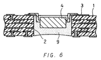
- FIG. 6 shows another variation in which a sealing resin 9 is filled in the opening 2 after the component 4 is received in the opening 2 of the PWB 1.
- the recess 10 can be formed by previously forming an opening sized to receive the component 4 in the core board and pre-impregnation excluding one core board, when a six patterned multilayer PWB is produced by laminating alternately three core board formed with double-sided copper foil patterns and two pre-impregnation.
- FIGs. 8-10 Though in FIG. 7, the conductive pad 3 to which the lead pins of the component 4 are electrically connected is formed on the PWB 1 as same as the first embodiment, in FIGs. 8-10, the conductive pads are formed on the exposed faces of the inner layers of the PWBs, namely, the conductive pads 3 are formed on the bottom of the recess 10.
- a moving coil (MC) type speaker or microphone is provided by forming a coiled conductive pattern 21a on the nonmagnetic vibration film 21 comprising plastic films, and electrically connecting it to the PWB 1. Alternating electric current flows in the coiled pattern 21a interlinking with the magnetic flux due to the magnet 19. The alternating current vibrates the vibration film 21 on which the coiled pattern 21a is formed. Otherwise, if the vibration film 21 vibrates, the magnetic flux interlinking with the coiled pattern 21a changes and thus, alternating current flows in the coiled pattern 21a.
- the magnet 19 is adhered to the bottom of the recess 16 of the PWB 1 with an epoxy-type adhesive.
Landscapes
- Engineering & Computer Science (AREA)
- Microelectronics & Electronic Packaging (AREA)
- Production Of Multi-Layered Print Wiring Board (AREA)
- Electric Connection Of Electric Components To Printed Circuits (AREA)
Abstract
Description
- This invention relates to a printed wiring board (PWB) for mounting a component including an electronic circuit, and an assembly of the same.
- As portable electronic equipment has become smaller and thinner, the mounting density of electronic components, such as semiconductor devices, resistors, capacitors, on PWBs has increased remarkably. Multilayer PWBs enable high-density mounting of such electronic components. A multilayer PWB, for example, is formed by laminating plural PWBs on which conductive circuit patterns are previously formed, and connecting the circuit patterns of the PWBs with each other by a via hole.
- Published Unexamined Japanese Patent Application (Tokkai-Sho) No. 60-57999 discloses a multilayer wiring board, where the inner layer patterns of the laminated PWBs are partially exposed in step-wise, and a conductive pad is connected to the exposed conductive patterns. In a general multilayer wiring board, a conductive pad is provided only to the outer layer, therefore, many via holes are necessary to connect the exterior patterns and the inner layer patterns. On the other hand, the multilayer wiring board disclosed in this reference can reduce the number of the via holes by providing another conductive pad to the exposed portion of the inner layer. This reference, however, does not disclose how to connect the conductive pad provided to the exposed portion of the inner layer to the electronic component, or how to produce such a multilayer wiring board.
- Published Examined Japanese Patent Application (Tokkoh-Hei) No. 5-41039 discloses a PWB, where a recess is provided by counterbore processing, and a semiconductor device is placed in the recess. The semiconductor device and the conductive pad of every layer are connected by a bonding wire, and sealed with resin. In this way, the semiconductor device is contained without substantially exceeding the thickness of the PWB. This method depends on connection by the bonding wires, and thus, this reference does not disclose application of the method to a surface mounting technology (SMT).
- FIG. 16 is a cross-sectional view to show the
PWB 31 to which acomponent 32 such as an integrated circuit is mounted by conventional surface mounting technology. Since alead pin 32a of thecomponent 32 is soldered to theconductive pad 33 on thePWB 31, thecomponent 32 is electrically connected and fixed to thePWB 31. - FIG. 17 shows an example where a
component 34, such as a speaker, is mounted on the surface of thePWB 31. Thecomponent 34 is fixed on thePWB 31 by anadhesive tape 35, while thelead wire 34a from thecomponent 34 is soldered to theconductive pad 33 on thePWB 31. - In a PWB assembly using SMT, the mounting area is reduced due to the high density trend, however, the assembly has not decreased significantly in thickness. Especially, when a comparatively large component such as a package semiconductor (e.g. IC, LSI), a speaker, or a microphone is mounted, the component becomes much higher than the surface of the wiring board.
- Therefore, an assembly using a conventional multilayer PWB does not meet the requirements for thin portable electronic equipment. If the assembly is thick, the portable electronic equipment cannot be thin, and the design of such electronic equipment will be limited. Reduction of the assembly's weight is another important aim.
- This invention aims to provide a thin and light multilayer PWB and an assembly of the same in order to solve the above-identified problems of the conventional techniques.
- A first PWB assembly of this invention comprises a PWB having an opening for receiving a component that includes an electronic circuit, and a component placed in the opening, which is substantially thinner than the PWB and is electrically connected to the PWB. As a result, a thin assembly can be provided. If a second component is mounted on the component which is received in the opening, or if the second component is mounted stretching over the first component and the PWB, other advantages can be obtained. For instance, the PWB area can be reduced. The other preferable embodiments according to this configuration will be explained below.
- In a second PWB assembly of this invention, a component including an electronic circuit is placed in a recess formed in the PWB, and a connecting terminal provided to the bottom of the component is electrically connected to the conductive pad formed on the bottom of the recess by using a conductive adhesive layer. Examples of such an adhesive layer include a solder ball or a two-step protruded electrode and conductive adhesive. According to this configuration, a thin assembly can be provided, and a plurality of components can be mounted on the recess with a high density.
- Such a recess for receiving a component can be formed by partially removing one or more layers of the plural conductive layers and insulating layers that comprise the multilayer PWB. More specifically, the process for producing such a PWB comprises the steps of:
- a) preparing plural double-sided conductive layer boards manufactured by sandwiching an insulating layer between two conductive layers, and preparing at least one insulating layer board to be placed between the double-sided conductive layer boards;
- b) forming holes in each board of step a) for electric connection between the conductive layers, and forming a hole that defines a recess for receiving a component in all but at least one board;
- c) etching the conductive layers of the double-sided conductive layer boards of step b), so that a predetermined circuit pattern is left;
- d) electrically connecting the conductive layers of the etched double-sided conductive layer boards of step c); and
- e) laminating the double-sided conductive layer boards and at least one insulating layer board with holes aligned so as to form electric connection between the conductive layers and to form a recess for receiving the component, and heat-pressing the laminate.
- In a PWB assembly provided with a recess for component receiving, other embodiments can be used as the assembly having the opening, for instance, two components can be mounted one after another.
- It is preferable that the insulating layer board be made of a compressible base material impregnated with resin, so that weight can be minimized. In addition, the electrical resistance is reduced and stabilized when the conductive layers are electrically connected to each other by filling the hole for electrical connection formed on the compressible porous material with conductive paste. The detail is explained below.
- A third PWB assembly of this invention comprises a PWB having a recess, a vibration film provided to cover the recess, and a coiled conductive pattern placed opposing to the vibration film, so as to perform conversion between vibration of the vibration film and electric current flowing in the coiled conductive pattern. According to this configuration, it is possible to integrally form a speaker or a microphone with a PWB. In other words, the weight and cost can be reduced considerably compared to a case that the other component like a speaker or a microphone is mounted on the PWB. Various embodiments of this configuration will be mentioned in detail.
- In another configuration, a PWB comprises a recess or an opening formed on the PWB in order to integrally form a speaker or a microphone with the PWB, a vibration film provided to cover the recess or the opening, a coiled conductive pattern provided to the vibration film, and a magnet placed opposing to the vibration film, so as to perform conversion between vibration of the vibration film and electric current flowing in the coiled conductive pattern.
- FIG. 1 is a cross-sectional view to show a PWB assembly in a first embodiment of this invention.
- FIG. 2 is a cross-sectional view to show a variation of PWB assembly of FIG. 1.
- FIG. 3 is a cross-sectional view to show another variation of PWB assembly of FIG. 1.
- FIG. 4 is a cross-sectional view to show still another variation of PWB assembly of FIG. 1.
- FIG. 5 is a cross-sectional view to show still another variation of PWB assembly of FIG. 1.
- FIG. 6 is a cross-sectional view to show still another variation of PWB assembly of FIG. 1.
- FIG. 7 is a cross-sectional view to show a PWB assembly in a second embodiment of this invention.
- FIG. 8 is a cross-sectional view to show a variation of PWB assembly of FIG. 7.
- FIG. 9 is a cross-sectional view to show another variation of PWB assembly of FIG. 7.
- FIG. 10 is a cross-sectional view to show still another variation of PWB assembly of FIG. 7.
- FIG. 11 is a cross-sectional view to show a PWB assembly in a third embodiment of this invention.
- FIG. 12 is a plan view to show a coiled conductive pattern of the PWB assembly of FIG. 11.
- FIG. 13 is a cross-sectional view to show a variation of PWB assembly of FIG. 11.
- FIG. 14 is a cross-sectional view to show another variation of PWB assembly of FIG. 11.
- FIG. 15 is a cross-sectional view to show still another variation of PWB assembly of FIG. 11.
- FIG. 16 is a cross-sectional view to show an example of a conventional PWB assembly.
- FIG. 17 is a cross-sectional view to show another example of a conventional PWB assembly.
- Preferable embodiments of this invention are explained below in detail, referring to FIGs. 1-15.
- FIG. 1 is a cross-sectional view to show a PWB assembly of the first embodiment of this invention. The
PWB 1 comprises anopening 2, and acomponent 4 is received in theopening 2. As shown in FIG. 1, thecomponent 4 is thinner than thePWB 1. The lead pins extending from thecomponent 4 are electrically connected to theconductive pad 3 on thePWB 1 by soldering. - The
PWB 1 of this embodiment has an inner via hole (IVH) structure where six conductive layers and five insulating layers are laminated alternately and the layers are electrically connected to each other by a through hole (a via hole). This PWB can be produced in the following process. - First, a pre-impregnation is prepared by impregnating a nonwoven cloth of aramid fiber with uncured epoxy resin. The pre-impregnation sandwiched by two copper foils is heat-pressed for about one hour in the condition of 180°C, 40Kg/cm2, so that a double-sided copper-clad laminated board (a core board) is produced. Next, the copper-clad laminated board is provided with a hole. A hole of about 0.2-0.4mm in diameter is drilled for a through hole. An opening for component receiving is also formed by punch-pressing or router-pressing using an end mill. In this way, an opening of the component size is formed.
- Next, pattern-etching is conducted to remove the copper foils, though the copper foils are partially left for the formed hole. A photolithography method is generally used for the pattern etching of a high density PWB. In this method, the wiring pattern is printed on the core board to which a dry film is stuck, by using a mask film on which the wiring pattern is printed. Later, unnecessary dry film and copper foils are melted and removed, and thus, a desirable copper foil pattern is obtained.
- Both sides of the PWB are completely pattern-etched, and the whole parts of the PWB are copper-plated. Thus, the inner wall of the through hole is also copper-plated, so that the conductive layers are electrically connected to each other. The conductive layers also can be electrically connected to each other by other methods. For example, the layers can be electrically connected by filling conductive paste (a half-kneaded mixture of resin and powder of silver, copper etc.) in the hole for electric connection. If the layers are electrically connected to each other by such a conductive paste, the heat-pressing can be omitted during the process for producing the double-sided copper-clad laminated board. Heat-pressing is carried out in the end.
- Three kinds of core boards are prepared by forming predetermined copper-foil patterns on both sides. These three core boards and two pre-impregnation for insulating layers are laminated alternately, and heat-pressed for about one hour at 180°C, 40Kg/cm2. In this manner, a multilayer PWB where six copper foil patterns and five insulating layers are laminated alternately is provided. The multilayer PWB is about 0.3 to 2.0mm thick. An opening is formed on the pre-impregnation to be sandwiched between the core boards in order to correspond to the opening of the core boards. Such an opening in the pre-impregnation is also formed by a punch-pressing or a router processing using an end mill.
- Next, conductive layers are provided with a hole if they are not adjacent to each other and need to be electrically connected. Then, the inner wall of the through hole is plated and electrically connected. After that, a solder resist film is printed on the PWB if necessary. In this manner, a component is mounted on the completed multilayer PWB. In a surface mounting technology (SMT), a solder paste is applied to the conductive pad of the PWB by printing, and a connecting terminal of the component is put thereon. The conductive pad is heated at 200°C or higher by passing through a reflow furnace, and thus, the component terminal and the conductive pad are connected to each other by melting the solder.
- As the comparatively
big component 4 is received in the opening of themultilayer PWB 1, the thickness of the assembly is not substantially increased after mounting the component. Therefore, it is possible to reduce the thickness of the electronic equipment in which this PWB assembly is received. In addition, a light assembly can be provided in this embodiment, since the weight of the PWB is reduced by the volume of the opening. - The above-mentioned compressible porous material in which resin is impregnated is used as the insulating material, so that the weight of the PWB itself is considerably reduced compared to the case using other boards such as ceramics. When the conductive layers are electrically connected to each other (via hole connection) by filling conductive paste in the hole on the compressible porous material, the binder in the conductive paste is easily absorbed in the porous material through the hole wall. As a result, electric resistance at the via hole is decreased after heating-compression, and the electric connection between the conductive layers is stabilized.
- In some cases as mentioned below, it is preferable that the surface of the component received in the opening of the PWB and the surface of the same board are flush. In such a case, a compressible porous material is used for the insulating layer, so that the compressive rate is adjusted during heating-compressive process. As a result, the component surface and the surface of the PWB become flush since the thickness of the PWB can be easily adjusted for the component.
- FIGs. 2-6 show the variations of PWBs, in which the components are received in the PWB's openings and the components are thinner than the PWBs. FIG. 2 shows a variation in which a second component 5 is mounted on the
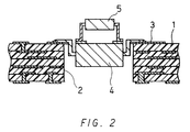
first component 4 which is received in theopening 2 of thePWB 1. If plural components are piled up as indicated in this drawing, several effects will be obtained, for instance, the mounting area can be reduced. In this invention, the level difference between the surface of the assembly and the PWB can be reduced. - FIG. 3 shows another variation in which a
second component 6 is mounted stretching over thefirst component 4 received in theopening 2 of thePWB 1. In a conventional technique, thefirst component 4 should be low and thesecond component 6 should have long legs for this mounting method. In this invention, however, such a mounting can be conducted easily even if thefirst component 4 is high. - FIG. 4 shows another variation in which a
second component 7 is mounted stretching over thefirst component 4 received in theopening 2 of thePWB 1 and the PWB itself. In a conventional technique, such a mounting will be difficult if the surface of thefirst component 4 is higher or lower than the surface of thePWB 1. However, it is rather easy in this invention. Therefore, it is preferable that the surface of thefirst component 4 is substantially flat and it is flush with the surface of thePWB 1. - FIG. 5 shows a variation in which the
opening 2 is covered with asheet member 8 after thecomponent 4 is received in theopening 2 of thePWB 1. Thesheet member 8 can have functions such as electric insulation, electromagnetic shield, heat sink, and moistureproof in order to compensate for the weak points of thecomponent 4. As a result, several effects can be obtained, for example, thecomponent 4 is electrically insulated from outside, effect of unnecessary radiation is controlled, or the temperature increase of thecomponent 4 is controlled. In addition, a second component (not shown) can be placed on thesheet member 8. In FIG. 5, thesheet members 8 are provided to the surface and back of the opening of the PWB, however, one of the sheet members may be omitted. - FIG. 6 shows another variation in which a sealing
resin 9 is filled in theopening 2 after thecomponent 4 is received in theopening 2 of thePWB 1. By filling the sealing resin, thecomponent 4 is fixed more strictly to thePWB 1 and the electric connection is stabilized. Another effect is that thecomponent 4 is protected from moisture. - In the above-mentioned embodiment and its variations, the multilayer PWBs can be replaced by one-sided PWBs or double-sided PWBs.
- In the above-mentioned embodiment and its variations, conductive pads for electric connection between the components and the PWBs are placed only on the front side of the PWBs. Such a conductive pad can also be placed on the back side of a multilayer PWB or a double-sided PWB. For instance, when a PWB has a component in its opening and lead pins extend from the both sides, the lead pins can be connected to the conductive pads on the front side and back side of the PWB.
- In the above-mentioned embodiment and its variations, the components and the PWBs can be electrically connected by conductive pads placed on the inner layers, not by the conductive pads on the PWBs. For instance, the opening may be formed with a stair-shape cross-section so that the conductive layer of the inner layer is partially exposed for connection to the conductive pad. In this way, the component received in the opening of the PWB will be thinner than the PWB, even if it includes the parts for electrical connection with the PWB. Another advantage is that the component having the electrical connection can be completely sealed with resin when the opening is filled with the sealing resin.
- FIG. 7 shows a cross-section of a PWB assembly in the second embodiment of this invention. The
PWB 1 has arecess 10 to receive thecomponent 4. Though such a recess can be formed by counterbore processing, another method, which is effective and excellent in mass-productivity can be chosen for a multilayer substrate. The recess 10 (see FIG. 7) of the multilayer PWB having six conductive layers and five insulating layers is formed by partially removing the four conductive layers and four insulating layers, and two conductive layers and one insulating layer are left. - For instance, in a method for producing a PWB explained in the first embodiment, the
recess 10 can be formed by previously forming an opening sized to receive thecomponent 4 in the core board and pre-impregnation excluding one core board, when a six patterned multilayer PWB is produced by laminating alternately three core board formed with double-sided copper foil patterns and two pre-impregnation. - This embodiment is especially suitable for a case in which the
component 4 should not be exposed from the back side of the PWB. In this embodiment, a light assembly can be provided as in the first embodiment, by preventing the surface of thecomponent 4 from being exposed from the surface of thePWB 1, more preferably, by forming thecomponent 4 and thePWB 1 to be flush. The variations (FIGs. 2-6) in the first embodiment can be used in this embodiment, too. In other words, the above-mentioned effects can be obtained by, for example, mounting another component on the component mounted on the recess, by mounting a component on the recess and covering the recess with a sheet member, or by filling a sealing resin in the recess. The other variations of this embodiment are shown in - FIGs. 8-10. Though in FIG. 7, the
conductive pad 3 to which the lead pins of thecomponent 4 are electrically connected is formed on thePWB 1 as same as the first embodiment, in FIGs. 8-10, the conductive pads are formed on the exposed faces of the inner layers of the PWBs, namely, theconductive pads 3 are formed on the bottom of therecess 10. - In FIG. 8, the lead pins of the
component 4 are soldered to theconductive pad 3 on the bottom of the recess. As mentioned in the first embodiment, the lead pins can be soldered by using solder paste at the same time that the other surface mounting components are soldered. - In FIGs. 9 and 10, the
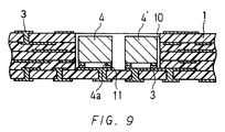
component 4 is provided with a terminal 4a for electrical connection on its bottom, instead of lead pins. This connecting terminal 4a is electrically connected by using an adhesive layer to theconductive pad 3 placed on the bottom of therecess 10 of thePWB 1. The adhesive layer is, for example, a solder ball or a conductive adhesive. The advantage of this mounting method is that plural components (4, 4') can be mounted with high density on the recess as shown in FIG. 9, and thus, it is suitable for bare chip mounting of a semiconductor. - In FIG. 9, the connecting terminal 4a of the component and the
conductive pad 3 are electrically connected through asolder ball 11. The solder ball is set on theconductive pad 3, and thecomponent 4 is temporarily fixed so that its terminal will be positioned on the soldering ball. As a result, the terminal of thecomponent 4 and theconductive pad 3 are connected to each other by melting the solder ball. - In FIG. 10, the connecting terminal 4a and the
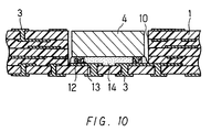
conductive pad 3 are electrically connected to each other by using a two-stage protruding electrode 12 and by using aconductive adhesive 13. Such a connecting method is called stud bump bonding (SBB). In FIG. 10, the two-stage protruding electrode 12 is adhered to the terminal side of thecomponent 4, and theconductive adhesive 13 is applied between the protrudingelectrode 12 and theconductive pad 3. Otherwise the conductive adhesive can be applied between the component terminal and the protruding electrode after the protruding electrode is adhered to the conductive pad side of the PWB. Anadhesive resin 14 is filled between the bottom of thecomponent 4 and the bottom of therecess 10 of thePWB 1 in order to improve the fixing strength. - FIG. 11 shows the cross section of the PWB assembly in a third embodiment of this invention. In this embodiment, a speaker (or a microphone) is composed of a
recess 16 formed on thePWB 1, amagnetic vibration film 17 placed to cover this recess, and a coiledconductive pattern 18 formed opposing to themagnetic vibration film 17. - The
coiled pattern 18 can be formed by using the copper foil of thePWB 1 as shown in the plan view of FIG. 12. Themagnetic vibration film 17 can be made by applying magnetic coating to plastic films such as polyethylene teraphthalate (PET), polyethylene naphthalate (PEN) or aramid, paper or nonwoven cloth, etc. Instead of applying the magnetic coating, magnetic powder can be added to the material of the plastic film. The periphery of the circularmagnetic vibration film 17 is adhered to the periphery of therecess 16 of thePWB 1 by using heat or adhesive materials. - When alternating current signal flows into the
coiled pattern 18, alternating flux generated by the signal crosses themagnetic vibration film 17, and thus, themagnetic vibration film 17 vibrates. In this manner, a speaker to convert the electric signal to the film vibration is provided. On the contrary, when the magnetizedmagnetic vibration film 17 vibrates, the magnetic flux interlinking with thecoiled pattern 18 changes. As a result, alternating current flows in thecoiled pattern 18. In this manner, a microphone to convert film vibration to electric current is provided. - As a variation shown in FIG. 13, the
magnetic vibration film 17 does not need to be magnetized if another recess 16' is provided to the backside of thePWB 1 and amagnet 19 is placed thereon. Namely, a magnetic type speaker or microphone is composed of amagnetic vibration film 17, acoiled pattern 18 and amagnet 19. In such a speaker or a microphone, magnetic field due to themagnet 7 changes as themagnetic vibration film 18 vibrates, and thus, alternating current is generated in the coiled pattern. Otherwise, themagnetic vibration film 8 vibrates due to the alternating current flowing in the coiled pattern. Themagnet 19 is adhered to the bottom of the recess 16' of thePWB 1 by using an epoxy-based adhesive. - In another variation shown in FIG. 14, a thin magnet (e.g. a rubber magnet) 20a is adhered to an nonmagnetic vibration film 20 comprising plastic films, so that the function of the film is as the same as that of the above-mentioned magnetized magnetic vibration film. Therefore, in this case, a so-called moving magnet (MM) type speaker or microphone is provided.
- In still another variation shown in FIG. 15, a moving coil (MC) type speaker or microphone is provided by forming a coiled
conductive pattern 21a on thenonmagnetic vibration film 21 comprising plastic films, and electrically connecting it to thePWB 1. Alternating electric current flows in thecoiled pattern 21a interlinking with the magnetic flux due to themagnet 19. The alternating current vibrates thevibration film 21 on which thecoiled pattern 21a is formed. Otherwise, if thevibration film 21 vibrates, the magnetic flux interlinking with thecoiled pattern 21a changes and thus, alternating current flows in thecoiled pattern 21a. Themagnet 19 is adhered to the bottom of therecess 16 of thePWB 1 with an epoxy-type adhesive. - In addition to the above-identified variations, several other variations to construct a speaker or a microphone can be made. By forming a speaker or a microphone integrated with a PWB, the cost for producing an assembly can be significantly decreased compared to the case where a speaker or a microphone as a separate component is mounted on a PWB. In this method, an increasingly light and thin assembly can be provided. The embodiments of this invention can be used for, e.g., electric devices such as portable phones.
- As mentioned above, this invention can provide a light and thin assembly by receiving a component in an opening or in a recess formed on a PWB and thus making the component thickness coextensive with the thickness of the PWB. In this embodiment, the area of the PWB can be reduced by mounting another component on the first component and the circuit patterns can be easily designed.
- In the method where a recess for receiving component by using a multilayer PWB, the circuit pattern can also be formed by printing, instead of etching. In this invention, the above-mentioned embodiments and their variations can be combined.
Claims (29)
- A printed wiring board assembly comprising:a printed wiring board having an opening for receiving an electrical component; andan electrical component placed in said opening, the electrical component being thinner than said printed wiring board and being electrically connected to said printed wiring board.
- The printed wiring board assembly according to claim 1, wherein said electrical component has a substantially flat surface, wherein the printed wiring board has an exterior surface, and wherein the flat surface of the component and the exterior surface of the printed wiring board are substantially flush.
- The printed wiring board assembly according to claim 1 or 2, wherein a second component is mounted on said first electrical component placed in said opening.
- The printed wiring board assembly according to claim 1 or 2, wherein a second component is mounted stretching over said electrical component.
- The printed wiring board according to any of claims 1 to 4, wherein a sheet member is provided to cover the opening of said printed wiring board.
- The printed wiring board assembly according to claim 5, wherein said sheet member has at least one function selected from the group consisting of electric insulation, electromagnetic shield, heat sink, and moisture protection.
- The printed wiring board assembly according to claim 5 or 6, wherein a second component is mounted on said sheet member.
- The printed wiring board according to any of claims 1 to 7, wherein a sealing resin is filled in the opening of said printed wiring board.
- The printed wiring board assembly according to any of claims 1 to 8,
wherein an insulating layer of said printed wiring board is made of a compressible porous base material impregnated with resin. - A multilayer printed wiring board produced by laminating plural conductive layers and insulating layers alternately, said multilayer printed wiring board comprising a recess for receiving a component.
- The multilayer printed wiring board according to claim 10, wherein said recess is formed by partially removing one or more layers of the plural conductive layers and insulating layers that comprise the multilayer printed wiring board.
- A method for producing a multilayer printed wiring board having a recess for receiving an electrical component, the method comprising:a) preparing plural double-sided conductive layer boards manufactured by sandwiching an insulating layer between two conductive layers, and preparing at least one insulating layer board to be placed between said double-sided conductive layer boards;b) forming holes in each board of step a) for electric connection between the conductive layers, and forming a hole that defines a recess for receiving a component in all but at least one board;c) etching the conductive layers of said double-sided conductive layer boards of step b), so that a predetermined circuit pattern is left;d) electrically connecting the conductive layers of the etched double-sided conductive layer boards of step c); ande) laminating the double-sided conductive layer boards and at least one insulating layer board with holes aligned so as to form electric connection between the conductive layers and to form the recess for receiving the electrical component, and heat-pressing the laminate.
- The method for producing a multilayer printed wiring board according to claim 12, wherein said at least one insulating layer board is made of a compressible porous base material impregnated with resin.
- A printed wiring board assembly wherein an electrical component is placed in a recess formed in a printed wiring board, and a connecting terminal provided to a bottom portion of the electrical component is electrically connected to a conductive pad formed on a bottom portion of said recess by using a conductive adhesive layer.
- The printed wiring board assembly according to claim 14, wherein the electrical component received in the recess of said printed wiring board is substantially lower than an exterior surface of said printed wiring board.
- The printed wiring board assembly according to claim 15, wherein a second component is mounted on said electrical component placed in said recess.
- The printed wiring board assembly according to claim 15, wherein a second component is mounted stretching over said electrical component and said recess.
- The printed wiring board assembly according to claim 15, wherein a sheet member is provided to cover the recess of said printed wiring board.
- The printed wiring board assembly according to claim 18, wherein said sheet member has at least one function selected from the group consisting of electric insulation, electromagnetic shield, heat sink, and moisture protection.
- The printed wiring board assembly according to claim 18 or 19, wherein a second component is mounted on said sheet member.
- The printed wiring board assembly according to any of claims 14 to 20, wherein a sealing resin is filled in the recess of said printed wiring board.
- The printed wiring board assembly according to any of claims 14 to 21, wherein a connecting terminal of said electrical component is electrically connected to a conductive pad on the bottom of said recess by using a solder ball.
- The printed wiring board assembly according to any of claims 14 to 21, wherein a connecting terminal of said electrical component is electrically connected to a conductive pad on the bottom of said recess by using a two-stage protruding electrode and a conductive adhesive material.
- The printed wiring board assembly according to any of claims 14 to 23, wherein an insulating layer of said printed wiring board is made of a compressible porous base material impregnated with resin.
- A printed wiring board assembly comprising:a printed wiring board having a recess;a vibration film provided to cover said recess; anda coiled conductive pattern disposed opposite said vibration film within said recess.
- The printed wiring board assembly according to claim 25, wherein a magnet is attached to said vibration film.
- The printed wiring board assembly according to claim 25, wherein said vibration film comprises a magnetic film.
- The printed wiring board assembly according to any of claims 25 to 27, further comprising a magnet placed on an opposite side of the printed wiring board from the vibration film.
- A printed wiring board assembly comprising:a printed wiring board having a recess;a vibration film provided to cover said recess;a coiled conductive pattern provided on said vibration film; anda magnet disposed opposite said vibration film within said recess.
Applications Claiming Priority (3)
| Application Number | Priority Date | Filing Date | Title |
|---|---|---|---|
| JP29832895 | 1995-11-16 | ||
| JP29832895 | 1995-11-16 | ||
| JP298328/95 | 1995-11-16 |
Publications (3)
| Publication Number | Publication Date |
|---|---|
| EP0774888A2 true EP0774888A2 (en) | 1997-05-21 |
| EP0774888A3 EP0774888A3 (en) | 1998-10-07 |
| EP0774888B1 EP0774888B1 (en) | 2003-03-19 |
Family
ID=17858245
Family Applications (1)
| Application Number | Title | Priority Date | Filing Date |
|---|---|---|---|
| EP19960118388 Expired - Lifetime EP0774888B1 (en) | 1995-11-16 | 1996-11-15 | Printed wiring board and assembly of the same |
Country Status (4)
| Country | Link |
|---|---|
| US (1) | US6324067B1 (en) |
| EP (1) | EP0774888B1 (en) |
| CN (1) | CN1094717C (en) |
| DE (1) | DE69626747T2 (en) |
Cited By (27)
| Publication number | Priority date | Publication date | Assignee | Title |
|---|---|---|---|---|
| EP0915641A1 (en) * | 1997-11-05 | 1999-05-12 | Nec Corporation | Surface mount assembly for electronic components |
| WO2002045463A2 (en) * | 2000-11-28 | 2002-06-06 | Knowles Electronics, Llc | Miniature silicon condenser microphone and method for producing same |
| GB2370421A (en) * | 2000-12-22 | 2002-06-26 | Ubinetics | Printed circuit board with recessed component |
| EP1225629A2 (en) * | 2001-01-19 | 2002-07-24 | Matsushita Electric Industrial Co., Ltd. | Component built-in module and method of manufacturing the same |
| GB2376594A (en) * | 2001-03-16 | 2002-12-18 | Nec Corp | Microphone unit mounting structure |
| KR20030032892A (en) * | 2001-10-18 | 2003-04-26 | 마쯔시다덴기산교 가부시키가이샤 | Component embedded module and manufacturing method thereof |
| SG99937A1 (en) * | 2000-08-31 | 2003-11-27 | Hitachi Ltd | An electronic device and a method of manufacturing the same |
| US6781231B2 (en) | 2002-09-10 | 2004-08-24 | Knowles Electronics Llc | Microelectromechanical system package with environmental and interference shield |
| EP1460888A1 (en) * | 2003-03-20 | 2004-09-22 | Alps Electric Co., Ltd. | Low-profile electronic circuit module and method for manufacturing the same |
| WO2005027602A1 (en) * | 2003-09-18 | 2005-03-24 | Imbera Electronics Oy | Method for manufacturing an electronic module |
| WO2005125298A2 (en) * | 2004-06-15 | 2005-12-29 | Imbera Electronics Oy | Method for manufacturing an electronics module comprising a component electrically connected to a conductor- pattern layer |
| WO2006023016A1 (en) * | 2004-08-19 | 2006-03-02 | Knowles Electronics, Llc | Silicon condenser microphone and manufacturing method |
| DE102005002751A1 (en) * | 2005-01-20 | 2006-08-24 | Alre-It Regeltechnik Gmbh | Printed circuit board, has recess, in which functional unit e.g. permanent magnet, is arranged, where recess is hole that is closed with punching part and thin layer and functional unit is bonded on thin section using adhesive |
| EP1821570A1 (en) * | 2000-11-28 | 2007-08-22 | Knowles Electronics, LLC | Miniature silicon condenser microphone and method for producing same |
| US7439616B2 (en) | 2000-11-28 | 2008-10-21 | Knowles Electronics, Llc | Miniature silicon condenser microphone |
| DE102008021750A1 (en) * | 2008-04-30 | 2009-11-05 | Endress + Hauser Gmbh + Co. Kg | Contactlessly identifiable electronic printed circuit board for measuring device, has radio frequency identification transponder inserted into recess, and electronic component comprising connection soldered on contact surface |
| WO2010028832A1 (en) * | 2008-09-12 | 2010-03-18 | Jabil Circuit, Inc. | Optical module for a cellular phone |
| US7894622B2 (en) | 2006-10-13 | 2011-02-22 | Merry Electronics Co., Ltd. | Microphone |
| US8240033B2 (en) | 2005-06-16 | 2012-08-14 | Imbera Electronics Oy | Method for manufacturing a circuit board |
| US8581109B2 (en) | 2005-06-16 | 2013-11-12 | Imbera Electronics Oy | Method for manufacturing a circuit board structure |
| US8617934B1 (en) | 2000-11-28 | 2013-12-31 | Knowles Electronics, Llc | Methods of manufacture of top port multi-part surface mount silicon condenser microphone packages |
| US9078063B2 (en) | 2012-08-10 | 2015-07-07 | Knowles Electronics, Llc | Microphone assembly with barrier to prevent contaminant infiltration |
| EP2988577A1 (en) * | 2014-08-20 | 2016-02-24 | AT & S Austria Technologie & Systemtechnik Aktiengesellschaft | Printed circuit board |
| US9374643B2 (en) | 2011-11-04 | 2016-06-21 | Knowles Electronics, Llc | Embedded dielectric as a barrier in an acoustic device and method of manufacture |
| US9794661B2 (en) | 2015-08-07 | 2017-10-17 | Knowles Electronics, Llc | Ingress protection for reducing particle infiltration into acoustic chamber of a MEMS microphone package |
| CN112312678A (en) * | 2019-09-29 | 2021-02-02 | 成都华微电子科技有限公司 | Structure and method of non-packaged chip direct-buried printed circuit board and chip packaging structure |
| EP3920673A1 (en) * | 2020-06-05 | 2021-12-08 | Littelfuse, Inc. | Flexible harness assembly for surface mounted devices |
Families Citing this family (129)
| Publication number | Priority date | Publication date | Assignee | Title |
|---|---|---|---|---|
| KR100514558B1 (en) * | 1998-09-09 | 2005-09-13 | 세이코 엡슨 가부시키가이샤 | Semiconductor device, method of manufacture thereof, circuit board, and electronic device |
| US6570994B1 (en) * | 1999-03-25 | 2003-05-27 | Agere Systems Inc. | Field layer speaker for consumer products |
| WO2000070677A1 (en) * | 1999-05-14 | 2000-11-23 | Seiko Epson Corporation | Semiconductor device, method of manufacture thereof, circuit board, and electronic device |
| JP2001144218A (en) * | 1999-11-17 | 2001-05-25 | Sony Corp | Semiconductor device and method of manufacture |
| EP1990831A3 (en) * | 2000-02-25 | 2010-09-29 | Ibiden Co., Ltd. | Multilayer printed circuit board and multilayer printed circuit board manufacturing method |
| TW511409B (en) * | 2000-05-16 | 2002-11-21 | Hitachi Aic Inc | Printed wiring board having cavity for mounting electronic parts therein and method for manufacturing thereof |
| TW533758B (en) * | 2000-07-31 | 2003-05-21 | Ngk Spark Plug Co | Printed wiring substrate and method for manufacturing the same |
| US6459593B1 (en) * | 2000-08-10 | 2002-10-01 | Nortel Networks Limited | Electronic circuit board |
| US7855342B2 (en) * | 2000-09-25 | 2010-12-21 | Ibiden Co., Ltd. | Semiconductor element, method of manufacturing semiconductor element, multi-layer printed circuit board, and method of manufacturing multi-layer printed circuit board |
| JP2003152317A (en) * | 2000-12-25 | 2003-05-23 | Ngk Spark Plug Co Ltd | Wiring board |
| TW574752B (en) * | 2000-12-25 | 2004-02-01 | Hitachi Ltd | Semiconductor module |
| JP3926141B2 (en) * | 2000-12-27 | 2007-06-06 | 日本特殊陶業株式会社 | Wiring board |
| JP2002204053A (en) * | 2001-01-04 | 2002-07-19 | Mitsubishi Electric Corp | Method and apparatus for mounting circuit as well as semiconductor device |
| JP2002314031A (en) * | 2001-04-13 | 2002-10-25 | Fujitsu Ltd | Multichip module |
| KR20020091785A (en) * | 2001-05-31 | 2002-12-06 | 니혼도꾸슈도교 가부시키가이샤 | Electronic parts and mobile communication device using the same |
| JP4810772B2 (en) * | 2001-07-31 | 2011-11-09 | パナソニック株式会社 | Circuit module |
| FI119215B (en) * | 2002-01-31 | 2008-08-29 | Imbera Electronics Oy | A method for immersing a component in a substrate and an electronic module |
| US8455994B2 (en) * | 2002-01-31 | 2013-06-04 | Imbera Electronics Oy | Electronic module with feed through conductor between wiring patterns |
| US7015616B2 (en) * | 2002-04-01 | 2006-03-21 | Honeywell International, Inc. | System and method for providing coil retention in the rotor windings of a high speed generator |
| US6680530B1 (en) | 2002-08-12 | 2004-01-20 | International Business Machines Corporation | Multi-step transmission line for multilayer packaging |
| TWI234210B (en) * | 2002-12-03 | 2005-06-11 | Sanyo Electric Co | Semiconductor module and manufacturing method thereof as well as wiring member of thin sheet |
| JP2004254138A (en) * | 2003-02-20 | 2004-09-09 | Sanyo Electric Co Ltd | Capacitor microphone |
| US7894203B2 (en) * | 2003-02-26 | 2011-02-22 | Ibiden Co., Ltd. | Multilayer printed wiring board |
| JP2005011837A (en) * | 2003-06-16 | 2005-01-13 | Nippon Micron Kk | Semiconductor device, substrate therefor, and its manufacturing method |
| DE10348620A1 (en) * | 2003-10-15 | 2005-06-02 | Infineon Technologies Ag | Semiconductor module with housing contacts |
| TW200404706A (en) * | 2003-12-05 | 2004-04-01 | Chung Shan Inst Of Science | Composite material structure for rotary-wings and its producing method |
| JP3961537B2 (en) * | 2004-07-07 | 2007-08-22 | 日本電気株式会社 | Manufacturing method of semiconductor mounting wiring board and manufacturing method of semiconductor package |
| US8487194B2 (en) * | 2004-08-05 | 2013-07-16 | Imbera Electronics Oy | Circuit board including an embedded component |
| JP2006054260A (en) | 2004-08-10 | 2006-02-23 | Toshiba Corp | Lsi package having interface function with outside, implementation having lsi package provided with interface function with outside and manufacturing method of implementation having lsi package provided with interface function with outside |
| JP4528062B2 (en) * | 2004-08-25 | 2010-08-18 | 富士通株式会社 | Semiconductor device and manufacturing method thereof |
| JP4028863B2 (en) | 2004-09-10 | 2007-12-26 | 富士通株式会社 | Substrate manufacturing method |
| KR20060026130A (en) * | 2004-09-18 | 2006-03-23 | 삼성전기주식회사 | Printed circuit board mounted chip-package and method for fabricating printed circuit board |
| US7317250B2 (en) * | 2004-09-30 | 2008-01-08 | Kingston Technology Corporation | High density memory card assembly |
| DE102004062547A1 (en) * | 2004-12-28 | 2006-07-13 | Siemens Ag | Electrical assembly with interconnected circuit carriers |
| US20060162957A1 (en) * | 2005-01-24 | 2006-07-27 | Jorg Kindermann | Printed circuit board, printed circuit module and method for producing a printed circuit board |
| US7968371B2 (en) * | 2005-02-01 | 2011-06-28 | Stats Chippac Ltd. | Semiconductor package system with cavity substrate |
| EP1691591A1 (en) * | 2005-02-09 | 2006-08-16 | Optimum Care International Tech. Inc. | Circuit board having recesses for inserting electronic components |
| DE102005008512B4 (en) | 2005-02-24 | 2016-06-23 | Epcos Ag | Electrical module with a MEMS microphone |
| DE102005008511B4 (en) | 2005-02-24 | 2019-09-12 | Tdk Corporation | MEMS microphone |
| US20060203457A1 (en) * | 2005-03-14 | 2006-09-14 | Tyco Electronics Power Systems, Inc. | Z-axis component connections for use in a printed wiring board |
| DE112006001506T5 (en) | 2005-06-16 | 2008-04-30 | Imbera Electronics Oy | Board structure and method for its production |
| DE102005032489B3 (en) * | 2005-07-04 | 2006-11-16 | Schweizer Electronic Ag | Circuit board multi-layer structure with integrated electric component, has insert embedded between two flat electrically insulating liquid resin structures |
| US7788801B2 (en) * | 2005-07-27 | 2010-09-07 | International Business Machines Corporation | Method for manufacturing a tamper-proof cap for an electronic module |
| US8101868B2 (en) * | 2005-10-14 | 2012-01-24 | Ibiden Co., Ltd. | Multilayered printed circuit board and method for manufacturing the same |
| US20070095564A1 (en) * | 2005-11-02 | 2007-05-03 | Ron Kozenitzky | Thin printed circuit board |
| DE102005053765B4 (en) | 2005-11-10 | 2016-04-14 | Epcos Ag | MEMS package and method of manufacture |
| DE102005053767B4 (en) | 2005-11-10 | 2014-10-30 | Epcos Ag | MEMS microphone, method of manufacture and method of installation |
| US20070111598A1 (en) * | 2005-11-14 | 2007-05-17 | Quilici James E | Electrical connector assemblies and methods of fabrication |
| KR20070056816A (en) * | 2005-11-30 | 2007-06-04 | 주식회사 유컴테크놀러지 | Rfid system |
| JP2007165383A (en) * | 2005-12-09 | 2007-06-28 | Ibiden Co Ltd | Printed wiring board having component mounting pin formed thereon |
| JP4654897B2 (en) * | 2005-12-09 | 2011-03-23 | イビデン株式会社 | Method for manufacturing printed wiring board having component mounting pins |
| JP4848752B2 (en) * | 2005-12-09 | 2011-12-28 | イビデン株式会社 | Printed wiring board having component mounting pins and electronic device using the same |
| WO2007069427A1 (en) * | 2005-12-15 | 2007-06-21 | Matsushita Electric Industrial Co., Ltd. | Module having built-in electronic component and method for manufacturing such module |
| KR100663549B1 (en) * | 2005-12-21 | 2007-01-02 | 삼성전자주식회사 | Semiconductor device package and method for manufacturing the same |
| US20070158811A1 (en) * | 2006-01-11 | 2007-07-12 | James Douglas Wehrly | Low profile managed memory component |
| WO2007086551A1 (en) * | 2006-01-27 | 2007-08-02 | Ibiden Co., Ltd. | Printed-circuit board, and method for manufacturing the same |
| JP4858538B2 (en) * | 2006-02-14 | 2012-01-18 | 株式会社村田製作所 | Multilayer ceramic electronic component, multilayer ceramic substrate, and method of manufacturing multilayer ceramic electronic component |
| KR100659510B1 (en) * | 2006-02-16 | 2006-12-20 | 삼성전기주식회사 | Method for manufacturing a substrate with cavity |
| JP3942190B1 (en) * | 2006-04-25 | 2007-07-11 | 国立大学法人九州工業大学 | Semiconductor device having double-sided electrode structure and manufacturing method thereof |
| KR20130023362A (en) * | 2006-05-24 | 2013-03-07 | 다이니폰 인사츠 가부시키가이샤 | Wiring board with built-in component and method for manufacturing wiring board with built-in component |
| JP2007317806A (en) * | 2006-05-24 | 2007-12-06 | Fujitsu Ltd | Printed board unit |
| DE102006036049A1 (en) * | 2006-08-02 | 2008-02-07 | Adc Automotive Distance Control Systems Gmbh | Electronic module for radiation sensor-component, has electronic components arranged in recess of printed circuit board as installation components such that electronic component do not project over board surface surrounding recess |
| JP2008085310A (en) * | 2006-08-28 | 2008-04-10 | Clover Denshi Kogyo Kk | Multilayer printed wiring board |
| JP5168863B2 (en) * | 2006-09-20 | 2013-03-27 | 日本電気株式会社 | Printed wiring board manufacturing method |
| KR100776189B1 (en) * | 2006-10-16 | 2007-11-16 | 주식회사 비에스이 | Mounting method for mounting microphone on flexible printed circuit board |
| US7982135B2 (en) * | 2006-10-30 | 2011-07-19 | Ibiden Co., Ltd. | Flex-rigid wiring board and method of manufacturing the same |
| US8203418B2 (en) * | 2007-01-11 | 2012-06-19 | Planarmag, Inc. | Manufacture and use of planar embedded magnetics as discrete components and in integrated connectors |
| US7821374B2 (en) | 2007-01-11 | 2010-10-26 | Keyeye Communications | Wideband planar transformer |
| KR101481682B1 (en) * | 2007-04-09 | 2015-01-12 | 삼성디스플레이 주식회사 | Touch screen display device |
| KR100885899B1 (en) * | 2007-04-27 | 2009-02-26 | 삼성전기주식회사 | PCB and manufacturing method thereof |
| CN101296566B (en) | 2007-04-29 | 2011-06-22 | 鸿富锦精密工业(深圳)有限公司 | Electric element carrier plate and manufacturing method thereof |
| TW200906263A (en) * | 2007-05-29 | 2009-02-01 | Matsushita Electric Ind Co Ltd | Circuit board and method for manufacturing the same |
| US7712210B2 (en) * | 2007-06-07 | 2010-05-11 | Endicott Interconnect Technologies, Inc. | Method of providing a printed circuit board with an edge connection portion |
| GB2451921A (en) * | 2007-08-17 | 2009-02-18 | Wolfson Microelectronics Plc | MEMS package |
| GB2451908B (en) * | 2007-08-17 | 2009-12-02 | Wolfson Microelectronics Plc | Mems package |
| JP5230997B2 (en) * | 2007-11-26 | 2013-07-10 | 新光電気工業株式会社 | Semiconductor device |
| US8259454B2 (en) * | 2008-04-14 | 2012-09-04 | General Electric Company | Interconnect structure including hybrid frame panel |
| JP4862017B2 (en) * | 2008-07-10 | 2012-01-25 | ルネサスエレクトロニクス株式会社 | Relay board, manufacturing method thereof, probe card |
| TWI363411B (en) * | 2008-07-22 | 2012-05-01 | Advanced Semiconductor Eng | Embedded chip substrate and fabrication method thereof |
| US8114708B2 (en) * | 2008-09-30 | 2012-02-14 | General Electric Company | System and method for pre-patterned embedded chip build-up |
| US8395054B2 (en) * | 2009-03-12 | 2013-03-12 | Ibiden Co., Ltd. | Substrate for mounting semiconductor element and method for manufacturing substrate for mounting semiconductor element |
| US8829355B2 (en) * | 2009-03-27 | 2014-09-09 | Ibiden Co., Ltd. | Multilayer printed wiring board |
| JPWO2010113448A1 (en) * | 2009-04-02 | 2012-10-04 | パナソニック株式会社 | Circuit board manufacturing method and circuit board |
| US20110051352A1 (en) * | 2009-09-02 | 2011-03-03 | Kim Gyu Han | Stacking-Type USB Memory Device And Method Of Fabricating The Same |
| EP2481269A1 (en) * | 2009-09-24 | 2012-08-01 | Option | System in package, printed circuit board provided with such system in package |
| KR101051491B1 (en) | 2009-10-28 | 2011-07-22 | 삼성전기주식회사 | Manufacturing method of multilayer flexible printed circuit board and multilayer flexible printed circuit board |
| US20110147069A1 (en) * | 2009-12-18 | 2011-06-23 | International Business Machines Corporation | Multi-tiered Circuit Board and Method of Manufacture |
| DE102010022204B4 (en) | 2010-05-20 | 2016-03-31 | Epcos Ag | Electric component with flat design and manufacturing process |
| US20110290540A1 (en) * | 2010-05-25 | 2011-12-01 | Samsung Electro-Mechanics Co., Ltd. | Embedded printed circuit board and method of manufacturing the same |
| US8649183B2 (en) * | 2011-02-10 | 2014-02-11 | Mulpin Research Laboratories, Ltd. | Electronic assembly |
| TWI473551B (en) | 2011-07-08 | 2015-02-11 | Unimicron Technology Corp | Package substrate and fabrication method thereof |
| DE102011051946A1 (en) * | 2011-07-19 | 2013-01-24 | Dorma Gmbh + Co. Kg | Door opener with means for detecting the position of moving parts of the door opener |
| TWI492680B (en) * | 2011-08-05 | 2015-07-11 | Unimicron Technology Corp | Package substrate having embedded interposer and fabrication method thereof |
| JP5768889B2 (en) * | 2011-09-07 | 2015-08-26 | 株式会社村田製作所 | Module manufacturing method and module |
| CN102739825A (en) * | 2012-06-13 | 2012-10-17 | 惠州Tcl移动通信有限公司 | Mainboard structure and mobile communication terminal |
| US9648744B2 (en) * | 2012-07-24 | 2017-05-09 | Apple Inc. | Ejectable component assemblies in electronic devices |
| KR101420526B1 (en) * | 2012-11-29 | 2014-07-17 | 삼성전기주식회사 | Substrate embedding electronic component and manufacturing mehtod thereof |
| US20140158414A1 (en) * | 2012-12-11 | 2014-06-12 | Chris Baldwin | Recessed discrete component mounting on organic substrate |
| JP2014116548A (en) * | 2012-12-12 | 2014-06-26 | Ngk Spark Plug Co Ltd | Multilayer wiring board and manufacturing method therefor |
| CN103281876A (en) * | 2013-05-28 | 2013-09-04 | 中国电子科技集团公司第十研究所 | Pit embedded circuit board three-dimensional assembling method |
| CN105934823A (en) | 2013-11-27 | 2016-09-07 | At&S奥地利科技与系统技术股份公司 | Circuit board structure |
| AT515101B1 (en) | 2013-12-12 | 2015-06-15 | Austria Tech & System Tech | Method for embedding a component in a printed circuit board |
| AT515447B1 (en) * | 2014-02-27 | 2019-10-15 | At & S Austria Tech & Systemtechnik Ag | Method for contacting a component embedded in a printed circuit board and printed circuit board |
| US11523520B2 (en) | 2014-02-27 | 2022-12-06 | At&S Austria Technologie & Systemtechnik Aktiengesellschaft | Method for making contact with a component embedded in a printed circuit board |
| DE102014105754B4 (en) | 2014-04-24 | 2022-02-10 | USound GmbH | Loudspeaker arrangement with circuit board integrated ASIC |
| USD785575S1 (en) * | 2014-05-28 | 2017-05-02 | Sumitomo Electric Industries, Ltd. | Flexible printed wiring board |
| US10192846B2 (en) | 2014-11-05 | 2019-01-29 | Infineon Technologies Austria Ag | Method of inserting an electronic component into a slot in a circuit board |
| JP6638262B2 (en) | 2015-02-03 | 2020-01-29 | 株式会社オートネットワーク技術研究所 | Circuit components |
| JP6333215B2 (en) * | 2015-05-19 | 2018-05-30 | オムロンオートモーティブエレクトロニクス株式会社 | Printed circuit boards, electronic devices |
| US9837484B2 (en) * | 2015-05-27 | 2017-12-05 | STATS ChipPAC Pte. Ltd. | Semiconductor device and method of forming substrate including embedded component with symmetrical structure |
| CN105025656A (en) * | 2015-07-24 | 2015-11-04 | 西安乾易企业管理咨询有限公司 | PCB reducing assembling and welding thickness and manufacture method of PCB |
| JP2017050315A (en) * | 2015-08-31 | 2017-03-09 | イビデン株式会社 | Printed wiring board and method of manufacturing the same |
| JP2017050313A (en) * | 2015-08-31 | 2017-03-09 | イビデン株式会社 | Printed wiring board and manufacturing method for printed wiring board |
| JP6602132B2 (en) * | 2015-09-24 | 2019-11-06 | キヤノン株式会社 | Printed circuit board |
| DE112015007224B4 (en) | 2015-12-23 | 2022-06-30 | Intel Corporation | Reverse Mounted Gull-Wing Electronics Housing |
| US11114353B2 (en) * | 2016-03-30 | 2021-09-07 | Intel Corporation | Hybrid microelectronic substrates |
| CN106206332B (en) * | 2016-07-17 | 2019-04-05 | 山东华芯电子有限公司 | A kind of manufacturing method of integrated circuit package structure |
| USD877099S1 (en) * | 2017-03-15 | 2020-03-03 | Sumitomo Electric Industries, Ltd. | Flexible printed wiring board for a module |
| US10390455B2 (en) * | 2017-03-27 | 2019-08-20 | Raytheon Company | Thermal isolation of cryo-cooled components from circuit boards or other structures |
| US10658772B1 (en) * | 2017-08-15 | 2020-05-19 | Adtran, Inc. | Tiered circuit board for interfacing cables and connectors |
| KR102397905B1 (en) | 2017-12-27 | 2022-05-13 | 삼성전자주식회사 | Interposer substrate and semiconductor package |
| US10804188B2 (en) | 2018-09-07 | 2020-10-13 | Intel Corporation | Electronic device including a lateral trace |
| CN109121293B (en) * | 2018-09-30 | 2020-05-15 | 西安易朴通讯技术有限公司 | Printed circuit board assembly and electronic device |
| WO2020181559A1 (en) * | 2019-03-14 | 2020-09-17 | 华为技术有限公司 | Method for machining circuit board, circuit board, electronic devices, terminal device |
| JP7024919B2 (en) * | 2019-07-09 | 2022-02-24 | 株式会社村田製作所 | Circuit board |
| US11723150B2 (en) * | 2020-09-04 | 2023-08-08 | Micron Technology, Inc. | Surface mount device bonded to an inner layer of a multi-layer substrate |
| US11641720B2 (en) * | 2020-09-18 | 2023-05-02 | Unimicron Technology Corp. | Circuit board and manufacturing method thereof |
| US11915986B2 (en) * | 2022-02-28 | 2024-02-27 | Texas Instruments Incorporated | Ceramic semiconductor device package with copper tungsten conductive layers |
| CN114615594A (en) * | 2022-03-01 | 2022-06-10 | 维沃移动通信有限公司 | Integrated circuit assembly and electronic device |
Family Cites Families (75)
| Publication number | Priority date | Publication date | Assignee | Title |
|---|---|---|---|---|
| US3852877A (en) * | 1969-08-06 | 1974-12-10 | Ibm | Multilayer circuits |
| US3770529A (en) * | 1970-08-25 | 1973-11-06 | Ibm | Method of fabricating multilayer circuits |
| US4080513A (en) * | 1975-11-03 | 1978-03-21 | Metropolitan Circuits Incorporated Of California | Molded circuit board substrate |
| JPS6034880B2 (en) * | 1976-12-06 | 1985-08-10 | 凸版印刷株式会社 | Manufacturing method of diaphragm |
| US4188513A (en) * | 1978-11-03 | 1980-02-12 | Northern Telecom Limited | Electret microphone with simplified electrical connections by printed circuit board mounting |
| DE2920012B1 (en) | 1979-05-17 | 1980-11-20 | Gao Ges Automation Org | ID card with IC module and method for producing such an ID card |
| DE3019207A1 (en) | 1980-05-20 | 1981-11-26 | GAO Gesellschaft für Automation und Organisation mbH, 8000 München | CARRIER ELEMENT FOR AN IC CHIP |
| JPS59175150A (en) * | 1983-03-24 | 1984-10-03 | Sharp Corp | Mounting structure of electronic component |
| JPS59181650A (en) * | 1983-03-31 | 1984-10-16 | Canon Inc | Printed circuit board sealed with circuit element |
| JPS6057999A (en) | 1983-09-09 | 1985-04-03 | 日本電気株式会社 | Multilayer circuit board |
| FR2556503B1 (en) * | 1983-12-08 | 1986-12-12 | Eurofarad | ALUMINA INTERCONNECTION SUBSTRATE FOR ELECTRONIC COMPONENT |
| DE3346461A1 (en) * | 1983-12-22 | 1985-07-04 | Siemens AG, 1000 Berlin und 8000 München | Method for manufacturing a telephone station |
| US4677528A (en) | 1984-05-31 | 1987-06-30 | Motorola, Inc. | Flexible printed circuit board having integrated circuit die or the like affixed thereto |
| US4783722A (en) * | 1985-07-16 | 1988-11-08 | Nippon Telegraph And Telephone Corporation | Interboard connection terminal and method of manufacturing the same |
| JPS62156847A (en) | 1985-12-28 | 1987-07-11 | Ibiden Co Ltd | Multilayer printed circuit board and manufacture thereof |
| US4871608A (en) * | 1986-12-10 | 1989-10-03 | Ngk Spark Plug Co., Ltd. | High-density wiring multilayered substrate |
| US4770922A (en) * | 1987-04-13 | 1988-09-13 | Japan Gore-Tex, Inc. | Printed circuit board base material |
| JP2549393B2 (en) * | 1987-10-02 | 1996-10-30 | 新光電気工業株式会社 | Circuit board manufacturing method |
| JPH0772092B2 (en) * | 1988-02-10 | 1995-08-02 | 日本特殊陶業株式会社 | Low temperature firing substrate |
| US5139851A (en) * | 1988-03-11 | 1992-08-18 | International Business Machines Corporation | Low dielectric composite substrate |
| US5139852A (en) * | 1988-03-11 | 1992-08-18 | International Business Machines Corporation | Low dielectric composite substrate |
| JPH0239587A (en) * | 1988-07-29 | 1990-02-08 | Oki Electric Ind Co Ltd | High density mounting printed board |
| JPH0287695A (en) * | 1988-09-26 | 1990-03-28 | Mitsubishi Electric Corp | Printed wiring board with surface packaging electronic part |
| US5031308A (en) * | 1988-12-29 | 1991-07-16 | Japan Radio Co., Ltd. | Method of manufacturing multilayered printed-wiring-board |
| JPH02268489A (en) * | 1989-04-11 | 1990-11-02 | Toyo Commun Equip Co Ltd | Printed board having sealed storing structure |
| JPH02268490A (en) * | 1989-04-11 | 1990-11-02 | Toyo Commun Equip Co Ltd | Printed board having storing section |
| JPH02301183A (en) * | 1989-05-15 | 1990-12-13 | Toshiba Corp | Manufacture of mounting type circuit component |
| JPH02301182A (en) * | 1989-05-16 | 1990-12-13 | Matsushita Electric Ind Co Ltd | Printed circuit board for flat mounting structure |
| US5116440A (en) * | 1989-08-09 | 1992-05-26 | Risho Kogyo Co., Ltd. | Process for manufacturing multilayer printed wiring board |
| US4964019A (en) | 1989-12-27 | 1990-10-16 | Ag Communication Systems Corporation | Multilayer bonding and cooling of integrated circuit devices |
| JPH03230597A (en) * | 1990-02-06 | 1991-10-14 | Mitsubishi Electric Corp | Semiconductor device mounting structure |
| DE4022829A1 (en) * | 1990-07-18 | 1992-01-23 | Werner Vogt | Electronic memory card - with connection leads aiding fixing of chip onto card |
| JPH0479360A (en) | 1990-07-23 | 1992-03-12 | Nec Corp | Semiconductor device |
| JPH04212446A (en) | 1990-09-04 | 1992-08-04 | Soshin Denki Kk | Thick film hybrid ic |
| JPH04263493A (en) * | 1991-02-18 | 1992-09-18 | Ibiden Co Ltd | Manufacture of printed wiring board |
| JPH06120670A (en) * | 1991-03-12 | 1994-04-28 | Japan Radio Co Ltd | Multilayer wiring board |
| US5274701A (en) * | 1991-05-29 | 1993-12-28 | Northern Telecom Limited | Telephone alerter |
| JPH0529747A (en) * | 1991-07-19 | 1993-02-05 | Akai Electric Co Ltd | Printed wiring board |
| JPH0582710A (en) | 1991-09-20 | 1993-04-02 | Hitachi Ltd | Package structure of semiconductor device |
| JPH05109952A (en) | 1991-10-15 | 1993-04-30 | Fujitsu Ltd | Semiconductor module |
| JPH05160540A (en) * | 1991-12-04 | 1993-06-25 | Seiko Epson Corp | Circuit board unit |
| US5367764A (en) | 1991-12-31 | 1994-11-29 | Tessera, Inc. | Method of making a multi-layer circuit assembly |
| JPH05226803A (en) * | 1992-02-10 | 1993-09-03 | Matsushita Electric Works Ltd | Mounting circuit board |
| JP3026465B2 (en) * | 1992-03-10 | 2000-03-27 | 株式会社日立製作所 | Ceramic thin film hybrid wiring board and manufacturing method |
| JP2823029B2 (en) | 1992-03-30 | 1998-11-11 | 日本電気株式会社 | Multi-chip module |
| JP2601128B2 (en) | 1992-05-06 | 1997-04-16 | 松下電器産業株式会社 | Method of manufacturing circuit forming substrate and circuit forming substrate |
| JP3006957B2 (en) * | 1992-05-13 | 2000-02-07 | 松下電器産業株式会社 | Semiconductor device package |
| JPH066043A (en) * | 1992-06-17 | 1994-01-14 | Tanaka Kikinzoku Kogyo Kk | Printed wiring board |
| US5828126A (en) * | 1992-06-17 | 1998-10-27 | Vlsi Technology, Inc. | Chip on board package with top and bottom terminals |
| US5729894A (en) * | 1992-07-21 | 1998-03-24 | Lsi Logic Corporation | Method of assembling ball bump grid array semiconductor packages |
| KR940008054A (en) * | 1992-09-01 | 1994-04-28 | 김광호 | Structure of Semiconductor Package |
| JPH0730059A (en) * | 1993-06-24 | 1995-01-31 | Nec Corp | Multichip module |
| US5412538A (en) * | 1993-07-19 | 1995-05-02 | Cordata, Inc. | Space-saving memory module |
| EP0645950B1 (en) | 1993-09-21 | 1998-09-02 | Matsushita Electric Industrial Co., Ltd. | Connecting member of a circuit substrate and method of manufacturing multilayer circuit substrates by using the same |
| CN1044762C (en) * | 1993-09-22 | 1999-08-18 | 松下电器产业株式会社 | Printed circuit board and method of manufacturing the same |
| US5386343A (en) * | 1993-11-12 | 1995-01-31 | Ford Motor Company | Double surface mount technology for electronic packaging |
| US5650918A (en) | 1993-11-25 | 1997-07-22 | Nec Corporation | Semiconductor device capable of preventing occurrence of a shearing stress |
| EP0658937A1 (en) | 1993-12-08 | 1995-06-21 | Hughes Aircraft Company | Vertical IC chip stack with discrete chip carriers formed from dielectric tape |
| EP0657932B1 (en) | 1993-12-13 | 2001-09-05 | Matsushita Electric Industrial Co., Ltd. | Chip package assembly and method of production |
| US5384689A (en) | 1993-12-20 | 1995-01-24 | Shen; Ming-Tung | Integrated circuit chip including superimposed upper and lower printed circuit boards |
| JPH07193164A (en) * | 1993-12-27 | 1995-07-28 | Nec Corp | Semiconductor integrated circuit device |
| JP3152559B2 (en) * | 1994-04-04 | 2001-04-03 | イビデン株式会社 | Semiconductor mounting board |
| JPH07288385A (en) | 1994-04-19 | 1995-10-31 | Hitachi Chem Co Ltd | Multilayer wiring board and its manufacture |
| US5468999A (en) | 1994-05-26 | 1995-11-21 | Motorola, Inc. | Liquid encapsulated ball grid array semiconductor device with fine pitch wire bonding |
| US5550403A (en) | 1994-06-02 | 1996-08-27 | Lsi Logic Corporation | Improved laminate package for an integrated circuit and integrated circuit having such a package |
| JPH07254766A (en) * | 1994-07-21 | 1995-10-03 | Akai Electric Co Ltd | Printed wiring board |
| US6031723A (en) * | 1994-08-18 | 2000-02-29 | Allen-Bradley Company, Llc | Insulated surface mount circuit board construction |
| US5567654A (en) | 1994-09-28 | 1996-10-22 | International Business Machines Corporation | Method and workpiece for connecting a thin layer to a monolithic electronic module's surface and associated module packaging |
| US5541450A (en) | 1994-11-02 | 1996-07-30 | Motorola, Inc. | Low-profile ball-grid array semiconductor package |
| US5542175A (en) | 1994-12-20 | 1996-08-06 | International Business Machines Corporation | Method of laminating and circuitizing substrates having openings therein |
| US5583376A (en) | 1995-01-03 | 1996-12-10 | Motorola, Inc. | High performance semiconductor device with resin substrate and method for making the same |
| US5701233A (en) | 1995-01-23 | 1997-12-23 | Irvine Sensors Corporation | Stackable modules and multimodular assemblies |
| TW373308B (en) * | 1995-02-24 | 1999-11-01 | Agere Systems Inc | Thin packaging of multi-chip modules with enhanced thermal/power management |
| US5616888A (en) | 1995-09-29 | 1997-04-01 | Allen-Bradley Company, Inc. | Rigid-flex circuit board having a window for an insulated mounting area |
| US5763947A (en) | 1996-01-31 | 1998-06-09 | International Business Machines Corporation | Integrated circuit chip package having configurable contacts and a removable connector |
-
1996
- 1996-11-15 DE DE1996626747 patent/DE69626747T2/en not_active Expired - Fee Related
- 1996-11-15 EP EP19960118388 patent/EP0774888B1/en not_active Expired - Lifetime
- 1996-11-15 CN CN96114469A patent/CN1094717C/en not_active Expired - Fee Related
-
2000
- 2000-04-20 US US09/553,557 patent/US6324067B1/en not_active Expired - Fee Related
Non-Patent Citations (1)
| Title |
|---|
| None |
Cited By (86)
| Publication number | Priority date | Publication date | Assignee | Title |
|---|---|---|---|---|
| US6310780B1 (en) | 1997-11-05 | 2001-10-30 | Nec Corporation | Surface mount assembly for electronic components |
| EP0915641A1 (en) * | 1997-11-05 | 1999-05-12 | Nec Corporation | Surface mount assembly for electronic components |
| SG99937A1 (en) * | 2000-08-31 | 2003-11-27 | Hitachi Ltd | An electronic device and a method of manufacturing the same |
| US9067780B1 (en) | 2000-11-28 | 2015-06-30 | Knowles Electronics, Llc | Methods of manufacture of top port surface mount MEMS microphones |
| US9096423B1 (en) | 2000-11-28 | 2015-08-04 | Knowles Electronics, Llc | Methods of manufacture of top port multi-part surface mount MEMS microphones |
| US10321226B2 (en) | 2000-11-28 | 2019-06-11 | Knowles Electronics, Llc | Top port multi-part surface mount MEMS microphone |
| US9338560B1 (en) | 2000-11-28 | 2016-05-10 | Knowles Electronics, Llc | Top port multi-part surface mount silicon condenser microphone |
| WO2002045463A3 (en) * | 2000-11-28 | 2003-05-15 | Knowles Electronics Llc | Miniature silicon condenser microphone and method for producing same |
| US8623709B1 (en) | 2000-11-28 | 2014-01-07 | Knowles Electronics, Llc | Methods of manufacture of top port surface mount silicon condenser microphone packages |
| US9156684B1 (en) | 2000-11-28 | 2015-10-13 | Knowles Electronics, Llc | Methods of manufacture of top port surface mount MEMS microphones |
| US9150409B1 (en) | 2000-11-28 | 2015-10-06 | Knowles Electronics, Llc | Methods of manufacture of bottom port surface mount MEMS microphones |
| US9148731B1 (en) | 2000-11-28 | 2015-09-29 | Knowles Electronics, Llc | Top port surface mount MEMS microphone |
| US9139422B1 (en) | 2000-11-28 | 2015-09-22 | Knowles Electronics, Llc | Bottom port surface mount MEMS microphone |
| US9139421B1 (en) | 2000-11-28 | 2015-09-22 | Knowles Electronics, Llc | Top port surface mount MEMS microphone |
| US9133020B1 (en) | 2000-11-28 | 2015-09-15 | Knowles Electronics, Llc | Methods of manufacture of bottom port surface mount MEMS microphones |
| WO2002045463A2 (en) * | 2000-11-28 | 2002-06-06 | Knowles Electronics, Llc | Miniature silicon condenser microphone and method for producing same |
| US9061893B1 (en) | 2000-11-28 | 2015-06-23 | Knowles Electronics, Llc | Methods of manufacture of top port multi-part surface mount silicon condenser microphones |
| US9051171B1 (en) | 2000-11-28 | 2015-06-09 | Knowles Electronics, Llc | Bottom port surface mount MEMS microphone |
| US9040360B1 (en) | 2000-11-28 | 2015-05-26 | Knowles Electronics, Llc | Methods of manufacture of bottom port multi-part surface mount MEMS microphones |
| US8623710B1 (en) | 2000-11-28 | 2014-01-07 | Knowles Electronics, Llc | Methods of manufacture of bottom port multi-part surface mount silicon condenser microphone packages |
| US9024432B1 (en) | 2000-11-28 | 2015-05-05 | Knowles Electronics, Llc | Bottom port multi-part surface mount MEMS microphone |
| US9006880B1 (en) | 2000-11-28 | 2015-04-14 | Knowles Electronics, Llc | Top port multi-part surface mount silicon condenser microphone |
| US8765530B1 (en) | 2000-11-28 | 2014-07-01 | Knowles Electronics, Llc | Methods of manufacture of top port surface mount silicon condenser microphone packages |
| US7166910B2 (en) | 2000-11-28 | 2007-01-23 | Knowles Electronics Llc | Miniature silicon condenser microphone |
| US8704360B1 (en) | 2000-11-28 | 2014-04-22 | Knowles Electronics, Llc | Top port surface mount silicon condenser microphone package |
| US7242089B2 (en) | 2000-11-28 | 2007-07-10 | Knowles Electronics, Llc | Miniature silicon condenser microphone |
| EP1821570A1 (en) * | 2000-11-28 | 2007-08-22 | Knowles Electronics, LLC | Miniature silicon condenser microphone and method for producing same |
| US8652883B1 (en) | 2000-11-28 | 2014-02-18 | Knowles Electronics, Llc | Methods of manufacture of bottom port surface mount silicon condenser microphone packages |
| US7381589B2 (en) | 2000-11-28 | 2008-06-03 | Knowles Electronics, Llc | Silicon condenser microphone and manufacturing method |
| US7434305B2 (en) | 2000-11-28 | 2008-10-14 | Knowles Electronics, Llc. | Method of manufacturing a microphone |
| US7439616B2 (en) | 2000-11-28 | 2008-10-21 | Knowles Electronics, Llc | Miniature silicon condenser microphone |
| US7537964B2 (en) | 2000-11-28 | 2009-05-26 | Knowles Electronics, Llc | Method of fabricating a miniature silicon condenser microphone |
| US8633064B1 (en) | 2000-11-28 | 2014-01-21 | Knowles Electronics, Llc | Methods of manufacture of top port multipart surface mount silicon condenser microphone package |
| US8624386B1 (en) | 2000-11-28 | 2014-01-07 | Knowles Electronics, Llc | Bottom port multi-part surface mount silicon condenser microphone package |
| US8629005B1 (en) | 2000-11-28 | 2014-01-14 | Knowles Electronics, Llc | Methods of manufacture of bottom port surface mount silicon condenser microphone packages |
| US8629552B1 (en) | 2000-11-28 | 2014-01-14 | Knowles Electronics, Llc | Top port multi-part surface mount silicon condenser microphone package |
| US8018049B2 (en) | 2000-11-28 | 2011-09-13 | Knowles Electronics Llc | Silicon condenser microphone and manufacturing method |
| US8629551B1 (en) | 2000-11-28 | 2014-01-14 | Knowles Electronics, Llc | Bottom port surface mount silicon condenser microphone package |
| US8624384B1 (en) | 2000-11-28 | 2014-01-07 | Knowles Electronics, Llc | Bottom port surface mount silicon condenser microphone package |
| US8624387B1 (en) | 2000-11-28 | 2014-01-07 | Knowles Electronics, Llc | Top port multi-part surface mount silicon condenser microphone package |
| US8624385B1 (en) | 2000-11-28 | 2014-01-07 | Knowles Electronics, Llc | Top port surface mount silicon condenser microphone package |
| US9023689B1 (en) | 2000-11-28 | 2015-05-05 | Knowles Electronics, Llc | Top port multi-part surface mount MEMS microphone |
| US8617934B1 (en) | 2000-11-28 | 2013-12-31 | Knowles Electronics, Llc | Methods of manufacture of top port multi-part surface mount silicon condenser microphone packages |
| GB2370421A (en) * | 2000-12-22 | 2002-06-26 | Ubinetics | Printed circuit board with recessed component |
| US6955948B2 (en) | 2001-01-19 | 2005-10-18 | Matsushita Electric Industrial Co., Ltd. | Method of manufacturing a component built-in module |
| KR100507791B1 (en) * | 2001-01-19 | 2005-08-17 | 마쯔시다덴기산교 가부시키가이샤 | Electric component embedded module and method of manufacturing the same |
| EP1225629A2 (en) * | 2001-01-19 | 2002-07-24 | Matsushita Electric Industrial Co., Ltd. | Component built-in module and method of manufacturing the same |
| EP1225629A3 (en) * | 2001-01-19 | 2003-07-16 | Matsushita Electric Industrial Co., Ltd. | Component built-in module and method of manufacturing the same |
| GB2376594A (en) * | 2001-03-16 | 2002-12-18 | Nec Corp | Microphone unit mounting structure |
| US6724905B2 (en) | 2001-03-16 | 2004-04-20 | Nec Corporation | Microphone unit mounting structure |
| GB2376594B (en) * | 2001-03-16 | 2005-07-06 | Nec Corp | Microphone unit mounting structure |
| US7294587B2 (en) | 2001-10-18 | 2007-11-13 | Matsushita Electric Industrial Co., Ltd. | Component built-in module and method for producing the same |
| KR20030032892A (en) * | 2001-10-18 | 2003-04-26 | 마쯔시다덴기산교 가부시키가이샤 | Component embedded module and manufacturing method thereof |
| US6975516B2 (en) | 2001-10-18 | 2005-12-13 | Matsushita Electric Industrial Co., Ltd. | Component built-in module and method for producing the same |
| US6781231B2 (en) | 2002-09-10 | 2004-08-24 | Knowles Electronics Llc | Microelectromechanical system package with environmental and interference shield |
| EP1460888A1 (en) * | 2003-03-20 | 2004-09-22 | Alps Electric Co., Ltd. | Low-profile electronic circuit module and method for manufacturing the same |
| GB2422054B (en) * | 2003-09-18 | 2007-05-16 | Imbera Electronics Oy | Method for manufacturing an electronic module |
| US11716816B2 (en) | 2003-09-18 | 2023-08-01 | Imberatek, Llc | Method for manufacturing an electronic module and electronic module |
| US10798823B2 (en) | 2003-09-18 | 2020-10-06 | Imberatek, Llc | Method for manufacturing an electronic module and electronic module |
| US9232658B2 (en) | 2003-09-18 | 2016-01-05 | Ge Embedded Electronics Oy | Method for manufacturing an electronic module |
| GB2422054A (en) * | 2003-09-18 | 2006-07-12 | Imbera Electronics Oy | Method for manufacturing an electronic module |
| US7696005B2 (en) | 2003-09-18 | 2010-04-13 | Imbera Electronics Oy | Method for manufacturing an electronic module in an installation base |
| WO2005027602A1 (en) * | 2003-09-18 | 2005-03-24 | Imbera Electronics Oy | Method for manufacturing an electronic module |
| WO2005125298A2 (en) * | 2004-06-15 | 2005-12-29 | Imbera Electronics Oy | Method for manufacturing an electronics module comprising a component electrically connected to a conductor- pattern layer |
| US8240032B2 (en) | 2004-06-15 | 2012-08-14 | Imbera Electronics Oy | Method for manufacturing an electronics module comprising a component electrically connected to a conductor-pattern layer |
| WO2005125298A3 (en) * | 2004-06-15 | 2006-10-26 | Imbera Electronics Oy | Method for manufacturing an electronics module comprising a component electrically connected to a conductor- pattern layer |
| EP2373060A3 (en) * | 2004-08-19 | 2014-05-28 | Knowles Electronics, LLC | Silicon condenser microphone and manufacturing method |
| WO2006023016A1 (en) * | 2004-08-19 | 2006-03-02 | Knowles Electronics, Llc | Silicon condenser microphone and manufacturing method |
| DE102005002751B4 (en) * | 2005-01-20 | 2012-06-14 | Alre-It Regeltechnik Gmbh | Circuit board with a functional element and method for positioning a functional element on a printed circuit board |
| DE102005002751A1 (en) * | 2005-01-20 | 2006-08-24 | Alre-It Regeltechnik Gmbh | Printed circuit board, has recess, in which functional unit e.g. permanent magnet, is arranged, where recess is hole that is closed with punching part and thin layer and functional unit is bonded on thin section using adhesive |
| US11792941B2 (en) | 2005-06-16 | 2023-10-17 | Imberatek, Llc | Circuit board structure and method for manufacturing a circuit board structure |
| US8581109B2 (en) | 2005-06-16 | 2013-11-12 | Imbera Electronics Oy | Method for manufacturing a circuit board structure |
| US9622354B2 (en) | 2005-06-16 | 2017-04-11 | Ge Embedded Electronics Oy | Method for manufacturing a circuit board structure |
| US11134572B2 (en) | 2005-06-16 | 2021-09-28 | Imberatek, Llc | Circuit board structure and method for manufacturing a circuit board structure |
| US8240033B2 (en) | 2005-06-16 | 2012-08-14 | Imbera Electronics Oy | Method for manufacturing a circuit board |
| US7894622B2 (en) | 2006-10-13 | 2011-02-22 | Merry Electronics Co., Ltd. | Microphone |
| DE102008021750A1 (en) * | 2008-04-30 | 2009-11-05 | Endress + Hauser Gmbh + Co. Kg | Contactlessly identifiable electronic printed circuit board for measuring device, has radio frequency identification transponder inserted into recess, and electronic component comprising connection soldered on contact surface |
| WO2010028832A1 (en) * | 2008-09-12 | 2010-03-18 | Jabil Circuit, Inc. | Optical module for a cellular phone |
| US8605210B2 (en) | 2008-09-12 | 2013-12-10 | Jabil Circuit, Inc. | Optical module for a cellular phone |
| US9374643B2 (en) | 2011-11-04 | 2016-06-21 | Knowles Electronics, Llc | Embedded dielectric as a barrier in an acoustic device and method of manufacture |
| US9078063B2 (en) | 2012-08-10 | 2015-07-07 | Knowles Electronics, Llc | Microphone assembly with barrier to prevent contaminant infiltration |
| WO2016026700A1 (en) * | 2014-08-20 | 2016-02-25 | At&S Austria Technologie & Systemtechnik Aktiengesellschaft | Printed circuit board |
| EP2988577A1 (en) * | 2014-08-20 | 2016-02-24 | AT & S Austria Technologie & Systemtechnik Aktiengesellschaft | Printed circuit board |
| US9794661B2 (en) | 2015-08-07 | 2017-10-17 | Knowles Electronics, Llc | Ingress protection for reducing particle infiltration into acoustic chamber of a MEMS microphone package |
| CN112312678A (en) * | 2019-09-29 | 2021-02-02 | 成都华微电子科技有限公司 | Structure and method of non-packaged chip direct-buried printed circuit board and chip packaging structure |
| EP3920673A1 (en) * | 2020-06-05 | 2021-12-08 | Littelfuse, Inc. | Flexible harness assembly for surface mounted devices |
Also Published As
| Publication number | Publication date |
|---|---|
| EP0774888B1 (en) | 2003-03-19 |
| DE69626747D1 (en) | 2003-04-24 |
| CN1094717C (en) | 2002-11-20 |
| EP0774888A3 (en) | 1998-10-07 |
| US6324067B1 (en) | 2001-11-27 |
| DE69626747T2 (en) | 2003-09-04 |
| CN1156949A (en) | 1997-08-13 |
Similar Documents
| Publication | Publication Date | Title |
|---|---|---|
| EP0774888B1 (en) | Printed wiring board and assembly of the same | |
| JPH09199824A (en) | Printed wiring board and its mounting body | |
| US6542379B1 (en) | Circuitry with integrated passive components and method for producing | |
| US5817404A (en) | Printed circuit board | |
| JP4079699B2 (en) | Multilayer wiring circuit board | |
| KR100865060B1 (en) | Rigid-flex wiring board | |
| JP3057924B2 (en) | Double-sided printed circuit board and method of manufacturing the same | |
| CN108738233B (en) | Printed wiring board and switching regulator | |
| US20140225701A1 (en) | Printed wiring board | |
| KR20160059125A (en) | Element embedded printed circuit board and method of manufacturing the same | |
| JPH071821B2 (en) | Wiring board | |
| JP4814129B2 (en) | Wiring board with built-in components, Wiring board built-in components | |
| JPH01145891A (en) | Manufacture of circuit substrate with solder bump | |
| JPS62114247A (en) | Manufacture of chip carrier for electronic element | |
| JP2001291817A (en) | Electronic circuit device and multilayer printed wiring board | |
| JP2734625B2 (en) | Method for manufacturing multilayer wiring board | |
| JPH05283888A (en) | Printed wiring board and its manufacture | |
| JPH01194500A (en) | Substrate for multilayer interconnection | |
| TW202301931A (en) | Method for producing a printed circuit board, and printed circuit board having at least one embedded electronic component | |
| KR20000059562A (en) | Flexible Substrates of Multi Metal Layer | |
| JP2002026519A (en) | Printed-circuit board and its manufacturing method | |
| JPS6192848A (en) | Manufacture of laminated board for metallic base printed wiring board | |
| JP2004273718A (en) | Wiring board | |
| KR20200121208A (en) | Manufacturing method of embedded printed circuit board using unclad | |
| JP2002076537A (en) | Printed wiring board reduced in electromagnetic interference and electronic equipment using it |
Legal Events
| Date | Code | Title | Description |
|---|---|---|---|
| PUAI | Public reference made under article 153(3) epc to a published international application that has entered the european phase |
Free format text: ORIGINAL CODE: 0009012 |
|
| AK | Designated contracting states |
Kind code of ref document: A2 Designated state(s): DE FR GB |
|
| PUAL | Search report despatched |
Free format text: ORIGINAL CODE: 0009013 |
|
| AK | Designated contracting states |
Kind code of ref document: A3 Designated state(s): DE FR GB |
|
| 17P | Request for examination filed |
Effective date: 19981029 |
|
| 17Q | First examination report despatched |
Effective date: 20010703 |
|
| GRAG | Despatch of communication of intention to grant |
Free format text: ORIGINAL CODE: EPIDOS AGRA |
|
| GRAG | Despatch of communication of intention to grant |
Free format text: ORIGINAL CODE: EPIDOS AGRA |
|
| GRAG | Despatch of communication of intention to grant |
Free format text: ORIGINAL CODE: EPIDOS AGRA |
|
| GRAH | Despatch of communication of intention to grant a patent |
Free format text: ORIGINAL CODE: EPIDOS IGRA |
|
| RTI1 | Title (correction) |
Free format text: PRINTED WIRING BOARD AND ASSEMBLY OF THE SAME |
|
| GRAH | Despatch of communication of intention to grant a patent |
Free format text: ORIGINAL CODE: EPIDOS IGRA |
|
| GRAA | (expected) grant |
Free format text: ORIGINAL CODE: 0009210 |
|
| AK | Designated contracting states |
Designated state(s): DE FR GB |
|
| REG | Reference to a national code |
Ref country code: GB Ref legal event code: FG4D |
|
| REF | Corresponds to: |
Ref document number: 69626747 Country of ref document: DE Date of ref document: 20030424 Kind code of ref document: P |
|
| ET | Fr: translation filed | ||
| PLBE | No opposition filed within time limit |
Free format text: ORIGINAL CODE: 0009261 |
|
| STAA | Information on the status of an ep patent application or granted ep patent |
Free format text: STATUS: NO OPPOSITION FILED WITHIN TIME LIMIT |
|
| 26N | No opposition filed |
Effective date: 20031222 |
|
| PGFP | Annual fee paid to national office [announced via postgrant information from national office to epo] |
Ref country code: FR Payment date: 20061108 Year of fee payment: 11 |
|
| PGFP | Annual fee paid to national office [announced via postgrant information from national office to epo] |
Ref country code: DE Payment date: 20061109 Year of fee payment: 11 |
|
| PGFP | Annual fee paid to national office [announced via postgrant information from national office to epo] |
Ref country code: GB Payment date: 20061115 Year of fee payment: 11 |
|
| GBPC | Gb: european patent ceased through non-payment of renewal fee |
Effective date: 20071115 |
|
| PG25 | Lapsed in a contracting state [announced via postgrant information from national office to epo] |
Ref country code: DE Free format text: LAPSE BECAUSE OF NON-PAYMENT OF DUE FEES Effective date: 20080603 |
|
| REG | Reference to a national code |
Ref country code: FR Ref legal event code: ST Effective date: 20080930 |
|
| PG25 | Lapsed in a contracting state [announced via postgrant information from national office to epo] |
Ref country code: GB Free format text: LAPSE BECAUSE OF NON-PAYMENT OF DUE FEES Effective date: 20071115 |
|
| PG25 | Lapsed in a contracting state [announced via postgrant information from national office to epo] |
Ref country code: FR Free format text: LAPSE BECAUSE OF NON-PAYMENT OF DUE FEES Effective date: 20071130 |