EP0777311A2 - Combined data and power transmission - Google Patents
Combined data and power transmission Download PDFInfo
- Publication number
- EP0777311A2 EP0777311A2 EP96308041A EP96308041A EP0777311A2 EP 0777311 A2 EP0777311 A2 EP 0777311A2 EP 96308041 A EP96308041 A EP 96308041A EP 96308041 A EP96308041 A EP 96308041A EP 0777311 A2 EP0777311 A2 EP 0777311A2
- Authority
- EP
- European Patent Office
- Prior art keywords
- data signal
- threshold value
- line
- data
- signal
- Prior art date
- Legal status (The legal status is an assumption and is not a legal conclusion. Google has not performed a legal analysis and makes no representation as to the accuracy of the status listed.)
- Granted
Links
Images

Classifications
-
- H—ELECTRICITY
- H02—GENERATION; CONVERSION OR DISTRIBUTION OF ELECTRIC POWER
- H02J—CIRCUIT ARRANGEMENTS OR SYSTEMS FOR SUPPLYING OR DISTRIBUTING ELECTRIC POWER; SYSTEMS FOR STORING ELECTRIC ENERGY
- H02J13/00—Circuit arrangements for providing remote indication of network conditions, e.g. an instantaneous record of the open or closed condition of each circuitbreaker in the network; Circuit arrangements for providing remote control of switching means in a power distribution network, e.g. switching in and out of current consumers by using a pulse code signal carried by the network
- H02J13/00006—Circuit arrangements for providing remote indication of network conditions, e.g. an instantaneous record of the open or closed condition of each circuitbreaker in the network; Circuit arrangements for providing remote control of switching means in a power distribution network, e.g. switching in and out of current consumers by using a pulse code signal carried by the network characterised by information or instructions transport means between the monitoring, controlling or managing units and monitored, controlled or operated power network element or electrical equipment
- H02J13/00016—Circuit arrangements for providing remote indication of network conditions, e.g. an instantaneous record of the open or closed condition of each circuitbreaker in the network; Circuit arrangements for providing remote control of switching means in a power distribution network, e.g. switching in and out of current consumers by using a pulse code signal carried by the network characterised by information or instructions transport means between the monitoring, controlling or managing units and monitored, controlled or operated power network element or electrical equipment using a wired telecommunication network or a data transmission bus
-
- H—ELECTRICITY
- H02—GENERATION; CONVERSION OR DISTRIBUTION OF ELECTRIC POWER
- H02J—CIRCUIT ARRANGEMENTS OR SYSTEMS FOR SUPPLYING OR DISTRIBUTING ELECTRIC POWER; SYSTEMS FOR STORING ELECTRIC ENERGY
- H02J1/00—Circuit arrangements for dc mains or dc distribution networks
-
- Y—GENERAL TAGGING OF NEW TECHNOLOGICAL DEVELOPMENTS; GENERAL TAGGING OF CROSS-SECTIONAL TECHNOLOGIES SPANNING OVER SEVERAL SECTIONS OF THE IPC; TECHNICAL SUBJECTS COVERED BY FORMER USPC CROSS-REFERENCE ART COLLECTIONS [XRACs] AND DIGESTS
- Y02—TECHNOLOGIES OR APPLICATIONS FOR MITIGATION OR ADAPTATION AGAINST CLIMATE CHANGE
- Y02B—CLIMATE CHANGE MITIGATION TECHNOLOGIES RELATED TO BUILDINGS, e.g. HOUSING, HOUSE APPLIANCES OR RELATED END-USER APPLICATIONS
- Y02B90/00—Enabling technologies or technologies with a potential or indirect contribution to GHG emissions mitigation
- Y02B90/20—Smart grids as enabling technology in buildings sector
-
- Y—GENERAL TAGGING OF NEW TECHNOLOGICAL DEVELOPMENTS; GENERAL TAGGING OF CROSS-SECTIONAL TECHNOLOGIES SPANNING OVER SEVERAL SECTIONS OF THE IPC; TECHNICAL SUBJECTS COVERED BY FORMER USPC CROSS-REFERENCE ART COLLECTIONS [XRACs] AND DIGESTS
- Y02—TECHNOLOGIES OR APPLICATIONS FOR MITIGATION OR ADAPTATION AGAINST CLIMATE CHANGE
- Y02E—REDUCTION OF GREENHOUSE GAS [GHG] EMISSIONS, RELATED TO ENERGY GENERATION, TRANSMISSION OR DISTRIBUTION
- Y02E60/00—Enabling technologies; Technologies with a potential or indirect contribution to GHG emissions mitigation
-
- Y—GENERAL TAGGING OF NEW TECHNOLOGICAL DEVELOPMENTS; GENERAL TAGGING OF CROSS-SECTIONAL TECHNOLOGIES SPANNING OVER SEVERAL SECTIONS OF THE IPC; TECHNICAL SUBJECTS COVERED BY FORMER USPC CROSS-REFERENCE ART COLLECTIONS [XRACs] AND DIGESTS
- Y04—INFORMATION OR COMMUNICATION TECHNOLOGIES HAVING AN IMPACT ON OTHER TECHNOLOGY AREAS
- Y04S—SYSTEMS INTEGRATING TECHNOLOGIES RELATED TO POWER NETWORK OPERATION, COMMUNICATION OR INFORMATION TECHNOLOGIES FOR IMPROVING THE ELECTRICAL POWER GENERATION, TRANSMISSION, DISTRIBUTION, MANAGEMENT OR USAGE, i.e. SMART GRIDS
- Y04S20/00—Management or operation of end-user stationary applications or the last stages of power distribution; Controlling, monitoring or operating thereof
-
- Y—GENERAL TAGGING OF NEW TECHNOLOGICAL DEVELOPMENTS; GENERAL TAGGING OF CROSS-SECTIONAL TECHNOLOGIES SPANNING OVER SEVERAL SECTIONS OF THE IPC; TECHNICAL SUBJECTS COVERED BY FORMER USPC CROSS-REFERENCE ART COLLECTIONS [XRACs] AND DIGESTS
- Y04—INFORMATION OR COMMUNICATION TECHNOLOGIES HAVING AN IMPACT ON OTHER TECHNOLOGY AREAS
- Y04S—SYSTEMS INTEGRATING TECHNOLOGIES RELATED TO POWER NETWORK OPERATION, COMMUNICATION OR INFORMATION TECHNOLOGIES FOR IMPROVING THE ELECTRICAL POWER GENERATION, TRANSMISSION, DISTRIBUTION, MANAGEMENT OR USAGE, i.e. SMART GRIDS
- Y04S40/00—Systems for electrical power generation, transmission, distribution or end-user application management characterised by the use of communication or information technologies, or communication or information technology specific aspects supporting them
- Y04S40/12—Systems for electrical power generation, transmission, distribution or end-user application management characterised by the use of communication or information technologies, or communication or information technology specific aspects supporting them characterised by data transport means between the monitoring, controlling or managing units and monitored, controlled or operated electrical equipment
- Y04S40/124—Systems for electrical power generation, transmission, distribution or end-user application management characterised by the use of communication or information technologies, or communication or information technology specific aspects supporting them characterised by data transport means between the monitoring, controlling or managing units and monitored, controlled or operated electrical equipment using wired telecommunication networks or data transmission busses
Definitions
- This invention relates to combined data and power transmission arrangements.
- a combined data and power transmission arrangement may be used, for example, to distribute electrical power to various components in a vehicle, and also to transmit digital data signals between those components.
- a problem with combining data and power transmission on the same physical cable is that fluctuations in the power supply level, caused for example by variations in the power drawn by the load, can affect the data signal levels, and hence can result in corruption of the data.
- the data signal can be isolated from power voltage variations by capacitively coupling it to the line.
- a side effect of this is that the average level of the data will then depend on the data pattern, thus making the data pattern-sensitive.
- the object of the present invention is to provide a way of reducing or overcoming these problems.
- a combined data and power transmission arrangement comprising one or more power supplies and one or more loads interconnected by a power transmission line, and transmitters and receivers for transmitting a digital data signal over the transmission line,
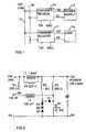
- Figure 1 is a block diagram of a combined data and power transmission arrangement in accordance with the invention, including two transmitter/receiver units.
- Figure 2 is a circuit diagram showing a transmitter circuit forming part of one of the transmitter/receiver units.
- Figure 3 is a circuit diagram showing a receiver circuit forming part of one of the transmitter/receiver units.
- the combined data and power transmission arrangement comprises two transmitter/receiver units 10, 11 interconnected by a line 12.
- One transmitter/receiver unit 10 is connected to a 12-volt DC power supply 13, while the other transmitter/receiver unit 11 is connected to an electrical load 14.
- Each of the transmitter/receiver units has a data input TXI for inputting data to be transmitted, and a data output RXO for outputting received data.
- the line 12 carries electrical power from the supply 13 to the load 14, and also carries data signals in both directions between the two transmitter/receiver units.
- the line may be a conventional 2-core power cable.
- the data transmission rate is approximately 200 Kbits per second.
- FIG. 1 shows the transmitter part of one of the transmitter/receiver units 10, 11.
- Each of the units 10, 11 includes a 1.5mH inductor L1, connected in series between the line 12 and the connected power supply 13 or load 14.
- the inductor presents a low resistance to DC current, and hence does not interfere with power transmission.
- the inductor presents relatively high impedance to the data signals, and hence acts as a barrier to those signals, preventing them from reaching the supply or load.
- the inductor L1 is constructed with 120 turns wound on an EP25 core with limbs.
- the input data signal TXI is applied to the gate of a FET (field effect transistor) Q1, which in this example is a VN1206 FET.
- the drain electrode of Q1 is connected to the line 12 by way of a 120 ⁇ H inductor L2, a 100nF capacitor C1, and a 220 Ohm resistor R1.
- the inductor L2 causes the transmitted data signal to have a relatively slow rise time of 0.5 microseconds, thus minimising RF radiation from the line.
- L2 is a small component, rated to carry only 10 milliamps without saturation.
- a chain of four diodes D1-D4 is connected between the source and drain electrodes of Q1. These diodes limit the voltage excursion of the drain electrode of Q1 to a maximum of 3V.
- a 220 Ohm resistor R4 is connected in parallel with L1. This, together with R1, gives a line matching impedance of 110 Ohms.
- the time constant of L1 with the resistors R1, R4 is 20 microseconds.
- Figure 3 shows the receiver part of one of the transmitter/receiver units 10, 11. It should be noted that, in Figure 3, the inductor L1 and the resistor R4 are shown again: these are the same components as shown in Figure 2.
- the data signal from the line 12 is coupled by way of a 2.2 nanofarad capacitor C5 to the inverting input (pin 3) of a high speed comparator circuit U1.
- the time constant of C5/R8 is 22 microseconds.
- the comparator circuit U1 compares the data signal with a threshold signal, applied to its positive input (pin 2).
- U1 produces a low output when the data signal is greater than the threshold, and a high output when the data signal is lower than the threshold.
- the output of U1 (pin 7) is fed to the data output terminal RXO.
- the threshold signal is a positive feedback signal, derived from the output of U1 by way of a potential divider chain, comprising a 100 KOhm resistor R9 and a 10 KOhm resistor R7.
- Resistor R7 has a 1 nanofarad capacitor C3 connected in parallel with it, to give a time constant of 9 microseconds. This time constant approximates the overall time constant of the transmitter components plus that of C5/R8, and ensures that the threshold signal tracks the mean level of the incoming data signal, and is independent of the data pattern.
- the receiver circuit is adaptive, in that the threshold level of the comparator tracks the average level of the incoming data, so as to ensure that fluctuations in the average signal level do not interfere with the correct reception of the data.
- a high frequency noise immunity of around 200 mV is maintained both during and in the absence of data transmission. At lower frequencies, higher noise immunity is obtained because of the low value of the AC coupling capacitor C5.
- Components R10, C4, D5 and D6 ensure that the output of the comparator is returned to a high level in the event that it has been low for a period in excess of 5 milliseconds; this being a requirement of the particular application.
- the comparison between the incoming data signal and the threshold could be performed digitally, using a digital signal processor.
- the power supply was a DC supply
- the invention could also be adapted to handle data transmission over the same line as an AC power supply.
Abstract
Description
- This invention relates to combined data and power transmission arrangements.
- A combined data and power transmission arrangement may be used, for example, to distribute electrical power to various components in a vehicle, and also to transmit digital data signals between those components.
- A problem with combining data and power transmission on the same physical cable is that fluctuations in the power supply level, caused for example by variations in the power drawn by the load, can affect the data signal levels, and hence can result in corruption of the data. The data signal can be isolated from power voltage variations by capacitively coupling it to the line. However, a side effect of this is that the average level of the data will then depend on the data pattern, thus making the data pattern-sensitive. The object of the present invention is to provide a way of reducing or overcoming these problems.
- According to the invention there is provided a combined data and power transmission arrangement comprising one or more power supplies and one or more loads interconnected by a power transmission line, and transmitters and receivers for transmitting a digital data signal over the transmission line,
- wherein the transmitter and receiver each include an inductor for providing a high impedance barrier to a data signal on the line, so as to isolate the data signal from the power supply and load,
- and wherein the receiver includes means for tracking the mid-point value of the data signal to produce a threshold value, and for comparing the threshold value with the data signal to produce an output signal.
- Figure 1 is a block diagram of a combined data and power transmission arrangement in accordance with the invention, including two transmitter/receiver units.
- Figure 2 is a circuit diagram showing a transmitter circuit forming part of one of the transmitter/receiver units.
- Figure 3 is a circuit diagram showing a receiver circuit forming part of one of the transmitter/receiver units.
- One combined data and power transmission arrangement in accordance with the invention will now be described by way of example with reference to the accompanying drawings.
- Referring to Figure 1, the combined data and power transmission arrangement comprises two transmitter/
receiver units line 12. One transmitter/receiver unit 10 is connected to a 12-voltDC power supply 13, while the other transmitter/receiver unit 11 is connected to anelectrical load 14. - Each of the transmitter/receiver units has a data input TXI for inputting data to be transmitted, and a data output RXO for outputting received data. The
line 12 carries electrical power from thesupply 13 to theload 14, and also carries data signals in both directions between the two transmitter/receiver units. The line may be a conventional 2-core power cable. The data transmission rate is approximately 200 Kbits per second. - Figure 2 shows the transmitter part of one of the transmitter/
receiver units - Each of the
units line 12 and the connectedpower supply 13 orload 14. The inductor presents a low resistance to DC current, and hence does not interfere with power transmission. On the other hand, the inductor presents relatively high impedance to the data signals, and hence acts as a barrier to those signals, preventing them from reaching the supply or load. In this example, the inductor L1 is constructed with 120 turns wound on an EP25 core with limbs. - The input data signal TXI is applied to the gate of a FET (field effect transistor) Q1, which in this example is a VN1206 FET. The drain electrode of Q1 is connected to the
line 12 by way of a 120µH inductor L2, a 100nF capacitor C1, and a 220 Ohm resistor R1. The inductor L2 causes the transmitted data signal to have a relatively slow rise time of 0.5 microseconds, thus minimising RF radiation from the line. L2 is a small component, rated to carry only 10 milliamps without saturation. The resonance of L2/C1, calculated at 50 KHz, was found to be no problem due to the heavy circuit damping of the series resistor R1. - A chain of four diodes D1-D4 is connected between the source and drain electrodes of Q1. These diodes limit the voltage excursion of the drain electrode of Q1 to a maximum of 3V.
- A fifth of this signal is launched down the line and this small signal (600mV at 10mA) also minimises RF radiation.
- A 220 Ohm resistor R4 is connected in parallel with L1. This, together with R1, gives a line matching impedance of 110 Ohms. The time constant of L1 with the resistors R1, R4 is 20 microseconds.
- Figure 3 shows the receiver part of one of the transmitter/
receiver units - The data signal from the
line 12 is coupled by way of a 2.2 nanofarad capacitor C5 to the inverting input (pin 3) of a high speed comparator circuit U1. The time constant of C5/R8 is 22 microseconds. The comparator circuit U1 compares the data signal with a threshold signal, applied to its positive input (pin 2). U1 produces a low output when the data signal is greater than the threshold, and a high output when the data signal is lower than the threshold. The output of U1 (pin 7) is fed to the data output terminal RXO. - The threshold signal is a positive feedback signal, derived from the output of U1 by way of a potential divider chain, comprising a 100 KOhm resistor R9 and a 10 KOhm resistor R7. Resistor R7 has a 1 nanofarad capacitor C3 connected in parallel with it, to give a time constant of 9 microseconds. This time constant approximates the overall time constant of the transmitter components plus that of C5/R8, and ensures that the threshold signal tracks the mean level of the incoming data signal, and is independent of the data pattern.
- As a result, it can be seen that the receiver circuit is adaptive, in that the threshold level of the comparator tracks the average level of the incoming data, so as to ensure that fluctuations in the average signal level do not interfere with the correct reception of the data. A high frequency noise immunity of around 200 mV is maintained both during and in the absence of data transmission. At lower frequencies, higher noise immunity is obtained because of the low value of the AC coupling capacitor C5.
- The system has been shown to stand up to transient loads sufficient to produce up to 6 V excursions from the 12 V load, before data corruption is encountered. With such a transient load, the excursion down the power line was measured at 4 V peak, with a maximum edge speed of 10 V/millisecond. Calculation shows that this will produce an offset voltage of 220 mV at pin 3 of U1 during the edge. This equates to the noise immunity of the receiver.
- Components R10, C4, D5 and D6 ensure that the output of the comparator is returned to a high level in the event that it has been low for a period in excess of 5 milliseconds; this being a requirement of the particular application.
- It will be appreciated that many modifications may be made to the system described above without departing from the scope of the present invention. For example, the component values given are by way of example only, and may be varied.
- In one possible modification, instead of using an analog comparator circuit such as U1, the comparison between the incoming data signal and the threshold could be performed digitally, using a digital signal processor.
- While in the above description the power supply was a DC supply, the invention could also be adapted to handle data transmission over the same line as an AC power supply.
Claims (6)
- A combined data and power transmission arrangement comprising one or more power supplies and loads interconnected by a power transmission line, and transmitters and receivers for transmitting a digital data signal over the transmission line,wherein the transmitter and receiver each include an inductor for providing a high impedance barrier to a data signal on the line, so as to isolate the data signal from the power supply and load,and wherein the receiver includes means for tracking the mid-point value of the data signal to produce a threshold value, and for comparing the threshold value with the data signal to produce an output signal.
- An arrangement according to Claim 1 wherein the receiver includes a comparator having a first input which receives the data signal from the line, a second input which receives the threshold value,
and wherein the threshold value comprises a controlled positive feedback signal derived from the output of the comparator. - An arrangement according to Claim 2 wherein the threshold value is derived from the output of the comparator by way of a positive feedback loop having a time constant approximately equal to the time constant of the transmitter.
- A transmitter/receiver circuit for use with a combined data and power transmission arrangement for transmitting digital data signals and power over a line, the circuit comprising:an inductor for providing a high impedance barrier to a data signal on the line, so as to isolate the data signals from a power supply and load,and means for tracking the mid-point value of a data signal to produce a threshold value, and for comparing the threshold value with the data signal to produce an output signal.
- A circuit according to Claim 4 including a comparator having a first input which receives the data signal from the line, a second input which receives the threshold value,
and wherein the threshold value comprises a controlled positive feedback signal derived from the output of the comparator. - A circuit according to Claim 5 wherein the threshold value is derived from the output of the comparator by way of a positive feedback loop having a time constant approximately equal to the time constant of the transmitter.
Applications Claiming Priority (2)
| Application Number | Priority Date | Filing Date | Title |
|---|---|---|---|
| GBGB9524948.8A GB9524948D0 (en) | 1995-12-06 | 1995-12-06 | Combined data and power transmission |
| GB9524948 | 1995-12-06 |
Publications (3)
| Publication Number | Publication Date |
|---|---|
| EP0777311A2 true EP0777311A2 (en) | 1997-06-04 |
| EP0777311A3 EP0777311A3 (en) | 1998-01-21 |
| EP0777311B1 EP0777311B1 (en) | 2001-08-08 |
Family
ID=10785002
Family Applications (1)
| Application Number | Title | Priority Date | Filing Date |
|---|---|---|---|
| EP96308041A Expired - Lifetime EP0777311B1 (en) | 1995-12-06 | 1996-11-06 | Combined data and power transmission |
Country Status (4)
| Country | Link |
|---|---|
| US (1) | US5859584A (en) |
| EP (1) | EP0777311B1 (en) |
| DE (1) | DE69614344T2 (en) |
| GB (1) | GB9524948D0 (en) |
Cited By (8)
| Publication number | Priority date | Publication date | Assignee | Title |
|---|---|---|---|---|
| GB2325313A (en) * | 1997-05-12 | 1998-11-18 | Fulleon Ltd | Electronic circuits for removing data signals from DC supply voltage |
| WO2001020748A1 (en) * | 1999-09-14 | 2001-03-22 | Siemens Aktiengesellschaft | Method for operating a building installation system |
| WO2002043220A1 (en) * | 2000-11-27 | 2002-05-30 | Point Lumineux | Wiring system for large-dimension block diagrams |
| WO2003047122A1 (en) * | 2001-11-29 | 2003-06-05 | Nokia Corporation | Transmission system for transmitting data via current conducting branches |
| WO2005062483A1 (en) * | 2003-12-23 | 2005-07-07 | Valeo Securite Habitacle (Sas) | Device for a wire connection to a remote electric board |
| EP1798834A3 (en) * | 2005-12-19 | 2009-05-06 | Power Integrations, Inc. | Method and apparatus to authenticate a power supply |
| FR2923666A1 (en) * | 2003-12-23 | 2009-05-15 | Valeo Securite Habitacle Sas | Wire connection device for detecting approach of user hand during access to vehicle, has separation circuit separating electric supply of signal transmitted to distant controller so that supply or signal wire is eliminated in cable bundle |
| WO2014117801A1 (en) * | 2013-01-29 | 2014-08-07 | Phonak Ag | State of charge indication in a hearing device |
Families Citing this family (78)
| Publication number | Priority date | Publication date | Assignee | Title |
|---|---|---|---|---|
| US6452482B1 (en) * | 1999-12-30 | 2002-09-17 | Ambient Corporation | Inductive coupling of a data signal to a power transmission cable |
| US6326704B1 (en) * | 1995-06-07 | 2001-12-04 | Automotive Technologies International Inc. | Vehicle electrical system |
| US6533316B2 (en) | 1995-06-07 | 2003-03-18 | Automotive Technologies International, Inc. | Automotive electronic safety network |
| US6733036B2 (en) | 1995-06-07 | 2004-05-11 | Automotive Technologies International, Inc. | Automotive electronic safety network |
| US6648367B2 (en) | 1995-06-07 | 2003-11-18 | Automotive Technologies International Inc. | Integrated occupant protection system |
| US9443358B2 (en) | 1995-06-07 | 2016-09-13 | Automotive Vehicular Sciences LLC | Vehicle software upgrade techniques |
| US7580782B2 (en) * | 1995-10-30 | 2009-08-25 | Automotive Technologies International, Inc. | Vehicular electronic system with crash sensors and occupant protection systems |
| US7744122B2 (en) | 1995-12-12 | 2010-06-29 | Automotive Technologies International, Inc. | Driver side aspirated airbags |
| US6144326A (en) | 1997-04-22 | 2000-11-07 | Silicon Laboratories, Inc. | Digital isolation system with ADC offset calibration |
| US6504864B1 (en) | 1997-04-22 | 2003-01-07 | Silicon Laboratories Inc. | Digital access arrangement circuitry and method for connecting to phone lines having a second order DC holding circuit |
| US6408034B1 (en) | 1997-04-22 | 2002-06-18 | Silicon Laboratories, Inc. | Framed delta sigma data with unlikely delta sigma data patterns |
| US6480602B1 (en) | 1997-04-22 | 2002-11-12 | Silicon Laboratories, Inc. | Ring-detect interface circuitry and method for a communication system |
| US6222922B1 (en) | 1997-04-22 | 2001-04-24 | Silicon Laboratories, Inc. | Loop current monitor circuitry and method for a communication system |
| US6137827A (en) | 1997-04-22 | 2000-10-24 | Silicon Laboratories, Inc. | Isolation system with digital communication across a capacitive barrier |
| US6289070B1 (en) | 1997-04-22 | 2001-09-11 | Silicon Laboratories, Inc. | Digital isolation system with ADC offset calibration including coarse offset |
| US6442213B1 (en) | 1997-04-22 | 2002-08-27 | Silicon Laboratories Inc. | Digital isolation system with hybrid circuit in ADC calibration loop |
| US6456712B1 (en) | 1997-04-22 | 2002-09-24 | Silicon Laboratories Inc. | Separation of ring detection functions across isolation barrier for minimum power |
| US6587560B1 (en) * | 1997-04-22 | 2003-07-01 | Silicon Laboratories Inc. | Low voltage circuits powered by the phone line |
| US5870046A (en) | 1997-04-22 | 1999-02-09 | Silicon Laboratories Inc. | Analog isolation system with digital communication across a capacitive barrier |
| US6167134A (en) * | 1997-04-22 | 2000-12-26 | Silicon Laboratories, Inc. | External resistor and method to minimize power dissipation in DC holding circuitry for a communication system |
| US6359983B1 (en) | 1997-04-22 | 2002-03-19 | Silicon Laboratories, Inc. | Digital isolation system with data scrambling |
| US6389134B1 (en) | 1997-04-22 | 2002-05-14 | Silicon Laboratories, Inc. | Call progress monitor circuitry and method for a communication system |
| US6442271B1 (en) | 1997-04-22 | 2002-08-27 | Silicon Laboratories, Inc. | Digital isolation system with low power mode |
| US6307891B1 (en) | 1997-04-22 | 2001-10-23 | Silicon Laboratories, Inc. | Method and apparatus for freezing a communication link during a disruptive event |
| US6498825B1 (en) * | 1997-04-22 | 2002-12-24 | Silicon Laboratories Inc. | Digital access arrangement circuitry and method for connecting to phone lines having a DC holding circuit with programmable current limiting |
| US6385235B1 (en) | 1997-04-22 | 2002-05-07 | Silicon Laboratories, Inc. | Direct digital access arrangement circuitry and method for connecting to phone lines |
| US6298133B1 (en) | 1997-04-22 | 2001-10-02 | Silicon Laboratories, Inc. | Telephone line interface architecture using ringer inputs for caller ID data |
| US6516024B1 (en) | 1997-04-22 | 2003-02-04 | Silicon Laboratories Inc. | Digital access arrangement circuitry and method for connecting to phone lines having a DC holding circuit with low distortion and current limiting |
| US6430229B1 (en) | 1997-04-22 | 2002-08-06 | Silicon Laboratories Inc. | Capacitive isolation system with digital communication and power transfer |
| US6339048B1 (en) * | 1999-12-23 | 2002-01-15 | Elementis Specialties, Inc. | Oil and oil invert emulsion drilling fluids with improved anti-settling properties |
| WO1999053627A1 (en) | 1998-04-10 | 1999-10-21 | Chrimar Systems, Inc. Doing Business As Cms Technologies | System for communicating with electronic equipment on a network |
| US6480510B1 (en) * | 1998-07-28 | 2002-11-12 | Serconet Ltd. | Local area network of serial intelligent cells |
| US10240935B2 (en) | 1998-10-22 | 2019-03-26 | American Vehicular Sciences Llc | Vehicle software upgrade techniques |
| US6249213B1 (en) * | 1998-12-17 | 2001-06-19 | Intel Corporation | Method for transmitting information over an alternating current power line through a plurality of frequency orthogonal subchannels |
| US6473608B1 (en) * | 1999-01-12 | 2002-10-29 | Powerdsine Ltd. | Structure cabling system |
| US6956826B1 (en) | 1999-07-07 | 2005-10-18 | Serconet Ltd. | Local area network for distributing data communication, sensing and control signals |
| US7154382B2 (en) * | 1999-12-30 | 2006-12-26 | Ambient Corporation | Arrangement of inductive couplers for data communication |
| US6549616B1 (en) | 2000-03-20 | 2003-04-15 | Serconet Ltd. | Telephone outlet for implementing a local area network over telephone lines and a local area network using such outlets |
| US6296355B1 (en) | 2000-03-22 | 2001-10-02 | Jean V Rittmann | Wire-frame eyewear assembly with transversely-lithe sidepiece element |
| US6961303B1 (en) | 2000-09-21 | 2005-11-01 | Serconet Ltd. | Telephone communication system and method over local area network wiring |
| US6791454B2 (en) * | 2000-11-17 | 2004-09-14 | Siemens Aktiengesellschaft | Cable |
| US20030018840A1 (en) * | 2001-07-18 | 2003-01-23 | Chandler Billy J. | Power bus information transmission system and method of data transmission |
| DE10340431B4 (en) * | 2002-09-03 | 2008-04-10 | Yazaki Corp. | Power line communication device for a vehicle |
| JP2004096600A (en) * | 2002-09-03 | 2004-03-25 | Yazaki Corp | Power source superimposition multiplex communication equipment for vehicle |
| IL152824A (en) | 2002-11-13 | 2012-05-31 | Mosaid Technologies Inc | Addressable outlet and a network using same |
| US6906618B2 (en) * | 2003-06-26 | 2005-06-14 | Abet Technologies, Llc | Method and system for bidirectional data and power transmission |
| IL159838A0 (en) | 2004-01-13 | 2004-06-20 | Yehuda Binder | Information device |
| US20060046766A1 (en) * | 2004-09-01 | 2006-03-02 | Abet Technologies, Llc | Method and system for bidirectional communications and power transmission |
| WO2006034323A2 (en) | 2004-09-21 | 2006-03-30 | Abet Technologies, Llc | Communication and ac power system |
| US20100207744A1 (en) * | 2004-11-10 | 2010-08-19 | Caterpillar Inc. | System And Method For Power And Data Delivery On A Machine |
| US8089345B2 (en) * | 2004-11-10 | 2012-01-03 | Caterpillar Inc. | System and method for power and data delivery on a machine |
| US8405500B2 (en) * | 2004-11-10 | 2013-03-26 | Caterpillar Inc. | System and method for power and data delivery on a machine |
| US20060097852A1 (en) * | 2004-11-10 | 2006-05-11 | Lammers Bryan G | System and method for power and data delivery on a machine |
| JP4356596B2 (en) * | 2004-11-26 | 2009-11-04 | ティアック株式会社 | Data transceiver |
| WO2006083935A2 (en) * | 2005-01-31 | 2006-08-10 | Abet Technologies, Llc | Secure computer system |
| US7352281B2 (en) * | 2005-02-22 | 2008-04-01 | Instrument Systems Inc. | Automotive gauge system using a power line carrier |
| US7215245B2 (en) * | 2005-05-31 | 2007-05-08 | Fu Ching Lee | Activator circuit responsive to power line disturbances |
| US7352282B2 (en) * | 2005-07-12 | 2008-04-01 | Yazaki Corporation | Communication system |
| US8532850B2 (en) * | 2009-03-17 | 2013-09-10 | General Electric Company | System and method for communicating data in locomotive consist or other vehicle consist |
| US8935022B2 (en) | 2009-03-17 | 2015-01-13 | General Electric Company | Data communication system and method |
| US8655517B2 (en) | 2010-05-19 | 2014-02-18 | General Electric Company | Communication system and method for a rail vehicle consist |
| US9379775B2 (en) | 2009-03-17 | 2016-06-28 | General Electric Company | Data communication system and method |
| US8702043B2 (en) | 2010-09-28 | 2014-04-22 | General Electric Company | Rail vehicle control communication system and method for communicating with a rail vehicle |
| US9637147B2 (en) | 2009-03-17 | 2017-05-02 | General Electronic Company | Data communication system and method |
| US8825239B2 (en) | 2010-05-19 | 2014-09-02 | General Electric Company | Communication system and method for a rail vehicle consist |
| US8798821B2 (en) | 2009-03-17 | 2014-08-05 | General Electric Company | System and method for communicating data in a locomotive consist or other vehicle consist |
| US8154153B2 (en) | 2007-01-25 | 2012-04-10 | Systems General Corp. | Method and apparatus for providing a communication channel through an output cable of a power supply |
| US20090195179A1 (en) * | 2008-02-05 | 2009-08-06 | Joseph Peter D | Power line communication |
| US8583299B2 (en) * | 2009-03-17 | 2013-11-12 | General Electric Company | System and method for communicating data in a train having one or more locomotive consists |
| US9513630B2 (en) | 2010-11-17 | 2016-12-06 | General Electric Company | Methods and systems for data communications |
| US10144440B2 (en) | 2010-11-17 | 2018-12-04 | General Electric Company | Methods and systems for data communications |
| US8914170B2 (en) | 2011-12-07 | 2014-12-16 | General Electric Company | System and method for communicating data in a vehicle system |
| WO2013096295A1 (en) | 2011-12-22 | 2013-06-27 | Enphase Energy, Inc. | Method and apparatus for transmitting combined power, control and data through an isolation barrier |
| GB2536907A (en) * | 2015-03-30 | 2016-10-05 | Lighting And Illumination Tech Experience Ltd | Controlling power to a load with signals along a power line |
| DE102016107694A1 (en) | 2015-05-11 | 2016-11-17 | Wimtec Sanitärprodukte Gmbh | Method for the wireless transmission of information |
| DE102015214754A1 (en) * | 2015-08-03 | 2017-02-09 | Robert Bosch Gmbh | Circuit element for data communication via a supply line |
| US10145666B2 (en) | 2016-12-19 | 2018-12-04 | Mitutoyo Corporation | Touch probe for CMM including digital signal communication |
| US10594367B1 (en) * | 2018-11-07 | 2020-03-17 | Linear Technology Holding Llc | Power over data lines system with accurate and simplified cable resistance sensing |
Citations (5)
| Publication number | Priority date | Publication date | Assignee | Title |
|---|---|---|---|---|
| US4029904A (en) * | 1974-11-27 | 1977-06-14 | U.S. Philips Corporation | Receiver circuit for automatic correction of DC level disturbances |
| JPS61208928A (en) * | 1985-03-13 | 1986-09-17 | Youei Seisakusho:Kk | Two-wire remote control system |
| US4633218A (en) * | 1983-12-19 | 1986-12-30 | Honeywell Inc. | Apparatus for receiving low level digital signals transmitted over power lines |
| EP0355532A2 (en) * | 1988-08-19 | 1990-02-28 | Siemens Aktiengesellschaft | Arrangement for transmitting data and supply voltage via a bus |
| US5391932A (en) * | 1993-07-20 | 1995-02-21 | Echelon Corporation | Source power coupler |
Family Cites Families (1)
| Publication number | Priority date | Publication date | Assignee | Title |
|---|---|---|---|---|
| US5644286A (en) * | 1993-10-04 | 1997-07-01 | Lockheed Martin Corporation | Power bus digital communication system |
-
1995
- 1995-12-06 GB GBGB9524948.8A patent/GB9524948D0/en active Pending
-
1996
- 1996-11-06 DE DE69614344T patent/DE69614344T2/en not_active Expired - Lifetime
- 1996-11-06 EP EP96308041A patent/EP0777311B1/en not_active Expired - Lifetime
- 1996-11-14 US US08/749,226 patent/US5859584A/en not_active Expired - Lifetime
Patent Citations (5)
| Publication number | Priority date | Publication date | Assignee | Title |
|---|---|---|---|---|
| US4029904A (en) * | 1974-11-27 | 1977-06-14 | U.S. Philips Corporation | Receiver circuit for automatic correction of DC level disturbances |
| US4633218A (en) * | 1983-12-19 | 1986-12-30 | Honeywell Inc. | Apparatus for receiving low level digital signals transmitted over power lines |
| JPS61208928A (en) * | 1985-03-13 | 1986-09-17 | Youei Seisakusho:Kk | Two-wire remote control system |
| EP0355532A2 (en) * | 1988-08-19 | 1990-02-28 | Siemens Aktiengesellschaft | Arrangement for transmitting data and supply voltage via a bus |
| US5391932A (en) * | 1993-07-20 | 1995-02-21 | Echelon Corporation | Source power coupler |
Non-Patent Citations (1)
| Title |
|---|
| PATENT ABSTRACTS OF JAPAN vol. 011, no. 046 (E-479), 12 February 1987 & JP 61 208928 A (YOUEI SEISAKUSHO:KK), 17 September 1986, * |
Cited By (15)
| Publication number | Priority date | Publication date | Assignee | Title |
|---|---|---|---|---|
| GB2325313A (en) * | 1997-05-12 | 1998-11-18 | Fulleon Ltd | Electronic circuits for removing data signals from DC supply voltage |
| GB2325313B (en) * | 1997-05-12 | 2001-06-13 | Fulleon Ltd | Electronic circuits |
| WO2001020748A1 (en) * | 1999-09-14 | 2001-03-22 | Siemens Aktiengesellschaft | Method for operating a building installation system |
| WO2002043220A1 (en) * | 2000-11-27 | 2002-05-30 | Point Lumineux | Wiring system for large-dimension block diagrams |
| US7327222B2 (en) | 2001-11-29 | 2008-02-05 | Nokia Corporation | Transmission system for transmitting data via current conducting branches |
| WO2003047122A1 (en) * | 2001-11-29 | 2003-06-05 | Nokia Corporation | Transmission system for transmitting data via current conducting branches |
| WO2005062483A1 (en) * | 2003-12-23 | 2005-07-07 | Valeo Securite Habitacle (Sas) | Device for a wire connection to a remote electric board |
| FR2923666A1 (en) * | 2003-12-23 | 2009-05-15 | Valeo Securite Habitacle Sas | Wire connection device for detecting approach of user hand during access to vehicle, has separation circuit separating electric supply of signal transmitted to distant controller so that supply or signal wire is eliminated in cable bundle |
| EP2190128A3 (en) * | 2003-12-23 | 2012-12-05 | Valeo Sécurité Habitacle | Device for a wire connection to a remote electric board |
| EP1798834A3 (en) * | 2005-12-19 | 2009-05-06 | Power Integrations, Inc. | Method and apparatus to authenticate a power supply |
| US8225111B2 (en) | 2005-12-19 | 2012-07-17 | Power Integrations, Inc. | Method and apparatus to authenticate a power supply |
| CN101017976B (en) * | 2005-12-19 | 2012-10-03 | 电力集成公司 | Method and apparatus to authenticate a power supply |
| US8499179B2 (en) | 2005-12-19 | 2013-07-30 | Power Integrations, Inc. | Method and apparatus to authenticate a power supply |
| WO2014117801A1 (en) * | 2013-01-29 | 2014-08-07 | Phonak Ag | State of charge indication in a hearing device |
| EP2952015B1 (en) | 2013-01-29 | 2019-10-30 | Sonova AG | State of charge indication in a hearing device |
Also Published As
| Publication number | Publication date |
|---|---|
| DE69614344D1 (en) | 2001-09-13 |
| US5859584A (en) | 1999-01-12 |
| EP0777311B1 (en) | 2001-08-08 |
| GB9524948D0 (en) | 1996-02-07 |
| EP0777311A3 (en) | 1998-01-21 |
| DE69614344T2 (en) | 2002-04-25 |
Similar Documents
| Publication | Publication Date | Title |
|---|---|---|
| EP0777311B1 (en) | Combined data and power transmission | |
| EP0572382B1 (en) | Three wire system for cochlear implant processor | |
| US6349223B1 (en) | Universal hand-free system for cellular phones in combination with vehicle's audio stereo system | |
| US4355303A (en) | Receiver for a distribution network power line carrier communication system | |
| US6515485B1 (en) | Method and system for power line impedance detection and automatic impedance matching | |
| EP0727900A2 (en) | Isolated high impedance, DC current sources for telecommunications applications | |
| KR100821422B1 (en) | Balanced transmission termination device and receiving device using the same | |
| EP0310237B1 (en) | Line build out circuits | |
| US6617965B1 (en) | Control of the level of the signal produced by a transceiver coupled to a power distribution line | |
| CZ2002597A3 (en) | Apparatus for feeding high-frequency transmitted signal into low-voltage mains | |
| US6445239B1 (en) | Bus coupling with amplitude-controlled transmission circuit | |
| US5109391A (en) | Unbalanced transmitter and receiver | |
| JPH0879190A (en) | Electromagnetic hazard preventing device for balanced transmission line | |
| US6639947B1 (en) | EMI reduction for isolated bus systems | |
| JP3130915B2 (en) | Data transmission equipment | |
| US20040183584A1 (en) | Communications device powered from host apparatus | |
| US6760380B1 (en) | Data transmission apparatus and method | |
| US5126601A (en) | Driver and receiver for a differential-signal electrical interface | |
| US3920925A (en) | Ground isolating circuit | |
| US6567472B1 (en) | System and method for terminating a line by reflecting a scaled impedance | |
| US7218892B2 (en) | Passive repeater/terminator | |
| JP3229134B2 (en) | Two-wire communication device | |
| US11251825B2 (en) | Data transmission device | |
| KR100587230B1 (en) | Direct current power apparatus for power line communication | |
| US20060146942A1 (en) | Arrangement for compensation of ground offset in a data bus system |
Legal Events
| Date | Code | Title | Description |
|---|---|---|---|
| PUAI | Public reference made under article 153(3) epc to a published international application that has entered the european phase |
Free format text: ORIGINAL CODE: 0009012 |
|
| AK | Designated contracting states |
Kind code of ref document: A2 Designated state(s): DE FR GB NL |
|
| 111L | Licence recorded |
Free format text: 970417 0100 DESIGN TO DISTRIBUTION LIMITED |
|
| PUAL | Search report despatched |
Free format text: ORIGINAL CODE: 0009013 |
|
| AK | Designated contracting states |
Kind code of ref document: A3 Designated state(s): DE FR GB NL |
|
| 17P | Request for examination filed |
Effective date: 19980530 |
|
| 17Q | First examination report despatched |
Effective date: 19990817 |
|
| GRAG | Despatch of communication of intention to grant |
Free format text: ORIGINAL CODE: EPIDOS AGRA |
|
| GRAG | Despatch of communication of intention to grant |
Free format text: ORIGINAL CODE: EPIDOS AGRA |
|
| GRAH | Despatch of communication of intention to grant a patent |
Free format text: ORIGINAL CODE: EPIDOS IGRA |
|
| GRAH | Despatch of communication of intention to grant a patent |
Free format text: ORIGINAL CODE: EPIDOS IGRA |
|
| GRAA | (expected) grant |
Free format text: ORIGINAL CODE: 0009210 |
|
| AK | Designated contracting states |
Kind code of ref document: B1 Designated state(s): DE FR GB NL |
|
| REF | Corresponds to: |
Ref document number: 69614344 Country of ref document: DE Date of ref document: 20010913 |
|
| REG | Reference to a national code |
Ref country code: GB Ref legal event code: IF02 |
|
| ET | Fr: translation filed | ||
| PLBE | No opposition filed within time limit |
Free format text: ORIGINAL CODE: 0009261 |
|
| STAA | Information on the status of an ep patent application or granted ep patent |
Free format text: STATUS: NO OPPOSITION FILED WITHIN TIME LIMIT |
|
| 26N | No opposition filed | ||
| PGFP | Annual fee paid to national office [announced via postgrant information from national office to epo] |
Ref country code: DE Payment date: 20091120 Year of fee payment: 14 |
|
| PGFP | Annual fee paid to national office [announced via postgrant information from national office to epo] |
Ref country code: NL Payment date: 20091112 Year of fee payment: 14 |
|
| PGFP | Annual fee paid to national office [announced via postgrant information from national office to epo] |
Ref country code: GB Payment date: 20091119 Year of fee payment: 14 Ref country code: FR Payment date: 20091201 Year of fee payment: 14 |
|
| REG | Reference to a national code |
Ref country code: NL Ref legal event code: V1 Effective date: 20110601 |
|
| GBPC | Gb: european patent ceased through non-payment of renewal fee |
Effective date: 20101106 |
|
| REG | Reference to a national code |
Ref country code: FR Ref legal event code: ST Effective date: 20110801 |
|
| REG | Reference to a national code |
Ref country code: DE Ref legal event code: R119 Ref document number: 69614344 Country of ref document: DE Effective date: 20110601 Ref country code: DE Ref legal event code: R119 Ref document number: 69614344 Country of ref document: DE Effective date: 20110531 |
|
| PG25 | Lapsed in a contracting state [announced via postgrant information from national office to epo] |
Ref country code: NL Free format text: LAPSE BECAUSE OF NON-PAYMENT OF DUE FEES Effective date: 20110601 |
|
| PG25 | Lapsed in a contracting state [announced via postgrant information from national office to epo] |
Ref country code: DE Free format text: LAPSE BECAUSE OF NON-PAYMENT OF DUE FEES Effective date: 20110531 |
|
| PG25 | Lapsed in a contracting state [announced via postgrant information from national office to epo] |
Ref country code: FR Free format text: LAPSE BECAUSE OF NON-PAYMENT OF DUE FEES Effective date: 20101130 |
|
| PG25 | Lapsed in a contracting state [announced via postgrant information from national office to epo] |
Ref country code: GB Free format text: LAPSE BECAUSE OF NON-PAYMENT OF DUE FEES Effective date: 20101106 |