EP0780904A2 - Article with array of light active units - Google Patents
Article with array of light active units Download PDFInfo
- Publication number
- EP0780904A2 EP0780904A2 EP96309251A EP96309251A EP0780904A2 EP 0780904 A2 EP0780904 A2 EP 0780904A2 EP 96309251 A EP96309251 A EP 96309251A EP 96309251 A EP96309251 A EP 96309251A EP 0780904 A2 EP0780904 A2 EP 0780904A2
- Authority
- EP
- European Patent Office
- Prior art keywords
- light control
- control unit
- lines
- light
- size
- Prior art date
- Legal status (The legal status is an assumption and is not a legal conclusion. Google has not performed a legal analysis and makes no representation as to the accuracy of the status listed.)
- Granted
Links
- 230000008439 repair process Effects 0.000 claims description 46
- 239000000758 substrate Substances 0.000 claims description 22
- 239000011159 matrix material Substances 0.000 claims description 10
- 238000000034 method Methods 0.000 description 16
- 239000002184 metal Substances 0.000 description 15
- 230000002093 peripheral effect Effects 0.000 description 9
- 229910021417 amorphous silicon Inorganic materials 0.000 description 7
- 238000003491 array Methods 0.000 description 7
- 238000003384 imaging method Methods 0.000 description 7
- 238000010586 diagram Methods 0.000 description 6
- 150000004767 nitrides Chemical class 0.000 description 6
- 230000007547 defect Effects 0.000 description 5
- 239000010409 thin film Substances 0.000 description 5
- 238000005516 engineering process Methods 0.000 description 4
- 239000000463 material Substances 0.000 description 4
- 238000012360 testing method Methods 0.000 description 4
- 239000003990 capacitor Substances 0.000 description 3
- WABPQHHGFIMREM-AKLPVKDBSA-N lead-210 Chemical compound [210Pb] WABPQHHGFIMREM-AKLPVKDBSA-N 0.000 description 3
- 150000003071 polychlorinated biphenyls Chemical class 0.000 description 3
- 230000008569 process Effects 0.000 description 3
- 239000003086 colorant Substances 0.000 description 2
- 230000003247 decreasing effect Effects 0.000 description 2
- 230000000694 effects Effects 0.000 description 2
- 238000003860 storage Methods 0.000 description 2
- 230000000007 visual effect Effects 0.000 description 2
- 241000282412 Homo Species 0.000 description 1
- 229910052581 Si3N4 Inorganic materials 0.000 description 1
- 238000004458 analytical method Methods 0.000 description 1
- 238000005452 bending Methods 0.000 description 1
- 230000008859 change Effects 0.000 description 1
- 239000004020 conductor Substances 0.000 description 1
- 239000013078 crystal Substances 0.000 description 1
- 238000005520 cutting process Methods 0.000 description 1
- 230000008030 elimination Effects 0.000 description 1
- 238000003379 elimination reaction Methods 0.000 description 1
- 239000011521 glass Substances 0.000 description 1
- AMGQUBHHOARCQH-UHFFFAOYSA-N indium;oxotin Chemical compound [In].[Sn]=O AMGQUBHHOARCQH-UHFFFAOYSA-N 0.000 description 1
- 239000011810 insulating material Substances 0.000 description 1
- 239000012212 insulator Substances 0.000 description 1
- 230000003993 interaction Effects 0.000 description 1
- 238000005304 joining Methods 0.000 description 1
- 238000003698 laser cutting Methods 0.000 description 1
- 239000004973 liquid crystal related substance Substances 0.000 description 1
- 238000002161 passivation Methods 0.000 description 1
- 229910021420 polycrystalline silicon Inorganic materials 0.000 description 1
- 229920005591 polysilicon Polymers 0.000 description 1
- 230000005855 radiation Effects 0.000 description 1
- 238000005070 sampling Methods 0.000 description 1
- HQVNEWCFYHHQES-UHFFFAOYSA-N silicon nitride Chemical compound N12[Si]34N5[Si]62N3[Si]51N64 HQVNEWCFYHHQES-UHFFFAOYSA-N 0.000 description 1
- 238000005476 soldering Methods 0.000 description 1
- 239000007787 solid Substances 0.000 description 1
- 230000007704 transition Effects 0.000 description 1
- 238000003466 welding Methods 0.000 description 1
Images


Classifications
-
- H—ELECTRICITY
- H01—ELECTRIC ELEMENTS
- H01L—SEMICONDUCTOR DEVICES NOT COVERED BY CLASS H10
- H01L27/00—Devices consisting of a plurality of semiconductor or other solid-state components formed in or on a common substrate
- H01L27/14—Devices consisting of a plurality of semiconductor or other solid-state components formed in or on a common substrate including semiconductor components sensitive to infrared radiation, light, electromagnetic radiation of shorter wavelength or corpuscular radiation and specially adapted either for the conversion of the energy of such radiation into electrical energy or for the control of electrical energy by such radiation
- H01L27/144—Devices controlled by radiation
- H01L27/146—Imager structures
- H01L27/14643—Photodiode arrays; MOS imagers
-
- G—PHYSICS
- G02—OPTICS
- G02F—OPTICAL DEVICES OR ARRANGEMENTS FOR THE CONTROL OF LIGHT BY MODIFICATION OF THE OPTICAL PROPERTIES OF THE MEDIA OF THE ELEMENTS INVOLVED THEREIN; NON-LINEAR OPTICS; FREQUENCY-CHANGING OF LIGHT; OPTICAL LOGIC ELEMENTS; OPTICAL ANALOGUE/DIGITAL CONVERTERS
- G02F1/00—Devices or arrangements for the control of the intensity, colour, phase, polarisation or direction of light arriving from an independent light source, e.g. switching, gating or modulating; Non-linear optics
- G02F1/01—Devices or arrangements for the control of the intensity, colour, phase, polarisation or direction of light arriving from an independent light source, e.g. switching, gating or modulating; Non-linear optics for the control of the intensity, phase, polarisation or colour
- G02F1/13—Devices or arrangements for the control of the intensity, colour, phase, polarisation or direction of light arriving from an independent light source, e.g. switching, gating or modulating; Non-linear optics for the control of the intensity, phase, polarisation or colour based on liquid crystals, e.g. single liquid crystal display cells
- G02F1/133—Constructional arrangements; Operation of liquid crystal cells; Circuit arrangements
- G02F1/1333—Constructional arrangements; Manufacturing methods
- G02F1/1343—Electrodes
- G02F1/134309—Electrodes characterised by their geometrical arrangement
- G02F1/134336—Matrix
-
- G—PHYSICS
- G02—OPTICS
- G02F—OPTICAL DEVICES OR ARRANGEMENTS FOR THE CONTROL OF LIGHT BY MODIFICATION OF THE OPTICAL PROPERTIES OF THE MEDIA OF THE ELEMENTS INVOLVED THEREIN; NON-LINEAR OPTICS; FREQUENCY-CHANGING OF LIGHT; OPTICAL LOGIC ELEMENTS; OPTICAL ANALOGUE/DIGITAL CONVERTERS
- G02F1/00—Devices or arrangements for the control of the intensity, colour, phase, polarisation or direction of light arriving from an independent light source, e.g. switching, gating or modulating; Non-linear optics
- G02F1/01—Devices or arrangements for the control of the intensity, colour, phase, polarisation or direction of light arriving from an independent light source, e.g. switching, gating or modulating; Non-linear optics for the control of the intensity, phase, polarisation or colour
- G02F1/13—Devices or arrangements for the control of the intensity, colour, phase, polarisation or direction of light arriving from an independent light source, e.g. switching, gating or modulating; Non-linear optics for the control of the intensity, phase, polarisation or colour based on liquid crystals, e.g. single liquid crystal display cells
- G02F1/1306—Details
- G02F1/1309—Repairing; Testing
-
- G—PHYSICS
- G02—OPTICS
- G02F—OPTICAL DEVICES OR ARRANGEMENTS FOR THE CONTROL OF LIGHT BY MODIFICATION OF THE OPTICAL PROPERTIES OF THE MEDIA OF THE ELEMENTS INVOLVED THEREIN; NON-LINEAR OPTICS; FREQUENCY-CHANGING OF LIGHT; OPTICAL LOGIC ELEMENTS; OPTICAL ANALOGUE/DIGITAL CONVERTERS
- G02F1/00—Devices or arrangements for the control of the intensity, colour, phase, polarisation or direction of light arriving from an independent light source, e.g. switching, gating or modulating; Non-linear optics
- G02F1/01—Devices or arrangements for the control of the intensity, colour, phase, polarisation or direction of light arriving from an independent light source, e.g. switching, gating or modulating; Non-linear optics for the control of the intensity, phase, polarisation or colour
- G02F1/13—Devices or arrangements for the control of the intensity, colour, phase, polarisation or direction of light arriving from an independent light source, e.g. switching, gating or modulating; Non-linear optics for the control of the intensity, phase, polarisation or colour based on liquid crystals, e.g. single liquid crystal display cells
- G02F1/133—Constructional arrangements; Operation of liquid crystal cells; Circuit arrangements
- G02F1/136—Liquid crystal cells structurally associated with a semi-conducting layer or substrate, e.g. cells forming part of an integrated circuit
- G02F1/1362—Active matrix addressed cells
- G02F1/136259—Repairing; Defects
- G02F1/136272—Auxiliary lines
-
- G—PHYSICS
- G02—OPTICS
- G02F—OPTICAL DEVICES OR ARRANGEMENTS FOR THE CONTROL OF LIGHT BY MODIFICATION OF THE OPTICAL PROPERTIES OF THE MEDIA OF THE ELEMENTS INVOLVED THEREIN; NON-LINEAR OPTICS; FREQUENCY-CHANGING OF LIGHT; OPTICAL LOGIC ELEMENTS; OPTICAL ANALOGUE/DIGITAL CONVERTERS
- G02F2201/00—Constructional arrangements not provided for in groups G02F1/00 - G02F7/00
- G02F2201/12—Constructional arrangements not provided for in groups G02F1/00 - G02F7/00 electrode
- G02F2201/123—Constructional arrangements not provided for in groups G02F1/00 - G02F7/00 electrode pixel
Abstract
Description
- The present invention relates to arrays of circuitry fabricated on substrates.
- US-A 5 464 984 describes an x-ray imaging system with a sensor array US-A 5 464 984 discloses that it is desirable to fabricate a large area array with contiguous edge-to-edge sensing of a radiation field. To accomplish this, non-imaging I/O circuitry of a sensor tile must reside interstitially in the imaging area of a pixel array. If the associated I/O pads and circuitry take up space on the imaging plane a loss of resolution and/or dead spots may occur in the image. US-A 5 464 984 also discloses an octagonal pixel architecture that can maintain high fill factor while allowing for adequate non-imaging area between the pixels to construct peripheral I/O circuitry. A transfer gate added between first and second rows is utilized to allow the first row to be read out and then used as an output shift register.
- The invention addresses a problem that arises in arrays of light active cells fabricated on substrates. Although conventional arrays are typically structured so that every light active cell has the same size, situations arise in which cells must have different sizes. When cells have different sizes, artifacts may arise that reduce image quality. A displayed image, for example, may have perceptible artifacts due to different cell sizes.
- Such artifacts can occur when a display array is constructed from distinct parts. Along a boundary between parts, a perceptible line may occur because a small additional space at the boundary enlarges the adjacent rows of cells slightly.
- US-A 5 464 984 ,cited above, discloses similar artifacts that arise in a tiled sensing array if each tile's I/O pads and circuitry take up space on the imaging plane. Resolution may be lost, and dead spots may occur.
- The invention is based on the discovery of a general technique that can alleviate the problem of different cell sizes. The technique spreads a difference in cell size across a series of cells to eliminate an artifact.
- The technique can be implemented in an article that includes a substrate and array circuitry at a surface of the substrate. The array circuitry includes an array of light active units, each with an effective size. The array circuitry also includes signal circuitry for receiving signals from or providing signals to the light active units. The array of light active units together interacts with images of an image size, for which there is a characteristic minimum size difference between adjacent light active units that is sufficient to produce an artifact in the application in which the array is used. That size difference is referred to herein as the "minimum artifact difference."
- A first light active unit has a first effective size, while a second has a second effective size smaller than the first by an overall size difference. The overall size difference is sufficient to produce an artifact in images having the image size were the first and second light active units adjacent each other. But the first and second light active units are separated by a spacing in which a subarray of intermediate light active units form a series of light active units extending from the first light active unit to the second light active unit. Within the series, each intermediate light active unit has an effective size less than the effective size of the preceding light active unit by a first size difference and greater than the effective size of the following light active unit by a second size difference. The first and second size differences of each intermediate light active unit are insufficient to produce an artifact in images having the image size.
- Because the differences are insufficient to produce an artifact, the artifact that would have resulted from the overall size difference is eliminated.
- The signal circuitry can include two sets of lines that cross, with each light active unit connected to one of each set of lines. The light active unit can be adjacent the region in which the lines to which it is connected cross.
- The article can be a display such as an active matrix liquid crystal display (AMLCD), and each light active unit can control presentation of a segment of images. Each unit's effective size can be its aperture area, determined by a spacing between lines that bound it or by an aperture boundary defined by a dark matrix. The overall size difference can result from a pair of scan lines or from a repair line parallel to and alongside one of the scan lines.
- In one aspect of the invention, there is provided an article comprising: a substrate with a surface at which circuitry can be formed; array circuitry formed at the surface of the substrate, the array circuitry comprising: an array of light active units; each light active unit having an effective size; the array of light active units together interacting with images having an image size; and signal circuitry for receiving signals from or providing signals to the light active units; the array of light active units including: a first light active unit that has a first effective size: a second light active unit that has second effective size smaller than the first effective size by an overall size difference; the overall size difference being sufficient to produce an artifact in images having the image size if the first and second light active units were adjacent to each other; the first and second light active units being separated in the array by a spacing; and a subarray of intermediate light active units in the spacing that form a series of light active units extending from the first light active unit to the second light active unit; each intermediate light active unit having an effective size less than the effective size of the light active unit preceding it in the series by a first size difference and greater than the effective size of the light active unit following it in the series by a second size difference; the first and second size differences of each intermediate light active unit being insufficient to produce an artifact in images having the image size.
- One embodiment of the invention is based on the recognition that the technique described above can produce special types of perceptible artifacts in displayed images. The human perceptual system is especially sensitive to line artifacts. A slight misalignment between light control units in a display can produce a perceptible artifact that appears as a break or bending defect in a line.
- This embodiment is further based on the discovery that these line artifacts can be reduced even though apertures of light control units have different sizes. If the effective centers of the light control unit apertures are evenly spaced, line artifacts are significantly lessened if not eliminated.
- The techniques described above are advantageous because they make it possible to provide an AMLCD with repair lines or with paired scan lines along a split without introducing artifacts due to differences in effective sizes of light control units. The techniques could reduce visibility of an artifact that would occur when a split array is formed by butting or joining two partial arrays.
- The invention will now be described by examples, with reference to the accompanying drawings, in which:
- Fig. 1 is a schematic diagram showing how a series of light active units in an array can have differences in effective sizes of adjacent units that are less than a minimum artifact difference even though the overall size difference is greater than the minimum artifact difference;
- Fig. 2 is a schematic diagram of a display array with paired lines, with a detail showing spacings between lines so that size differences of adjacent light control units are less than the minimum artifact difference;
- Fig. 3 is an alternative detail of the display array of Fig. 2, showing aperture boundaries defined by a dark matrix so that size differences of adjacent light control units are less than the minimum artifact difference;
- Fig. 4 is a schematic diagram showing a 4096 x 6144 split array with two repair structures, each with two repair lines along a split line;
- Fig. 5 is a schematic layout diagram showing a cell in the array of Fig. 4 in which a repair lines is parallel to and alongside a scan line;
- Fig. 6 is a schematic layout diagram showing sizes of rows of light control units near the split line in the array of Fig. 4:
- Fig. 7 is a cross sectional view along the line B-B in Fig. 5;
- Fig. 8 is a cross sectional view along the line C-C in Fig. 5;
- Fig. 9 is a flow chart showing acts in repairing open data lines in the array of Fig. 4; and
- Fig. 10 is a schematic diagram showing a repaired array produced by the technique of Fig. 9.
- In an array of circuitry, a cell is a "light active unit" if the cell includes circuitry that can interact with light, such as by sensing light, by emitting light, or by modifying reflected or transmitted light.
- An "image" is a pattern of physical light.
- An image may be divided into "segments," each of which is itself an image. A segment of an image may be of any size up to and including the whole image.
- The "effective size" of a light active unit is a measure of the segment of an image with which the light active unit interacts. The "effective area" of a two-dimensional light active unit is its effective size measured in two dimensions. The "boundary" of a light active unit's effective area is a line that surrounds its effective area.
- In an array, two light active units are "separated in the array by a spacing" if the spacing indicates the shortest distance between the boundaries of their effective areas.
- A "series of light active units" is a number of light active units that extend from a first light active unit to a last light active unit, within which each intermediate light active unit has a preceding light active unit and a following light active unit, and within which adjacent light active units are not separated by a spacing large enough for an additional light active unit.
- Intermediate light active units in a spacing between first and second light active units "form a series of light active units extending from the first light active unit to the second light active unit" if there is a series of light active units that extends from the first light active unit to the second and that includes, in addition, only the intermediate light active units.
- An "artifact" is an item of information about an image or another effect produced by an image that does not result from the image itself but that results due to a boundary or other difference between segments interacting with adjacent light active units. Artifacts typically result from sampling that is inherent in interacting with an image as an array of image segments. An artifact can be thought of as a type of spatially constant noise that is added to the image.
- In an array of light active units that together interact with images of an image size, a size difference between the effective sizes of two light active units is "sufficient to produce an artifact" in images having the image size if the light active units were adjacent if the ordinary use of the array would produce an artifact resulting from the size difference if the light active units were adjacent.
- The "minimum artifact difference" for interactions of an array of light active units with images of an image size is a characteristic minimum size difference between adjacent light active units that is sufficient to produce an artifact in the application in which the array is used.
- A "light control unit" is a light active unit that is structured to receive a signal and to respond to its signal by causing presentation of an image segment with one of a set of colors; in a monochrome display, the colors are different levels of brightness of a single hue.
- The "effective aperture area" of a light control unit is the effective area of image segments that the light control unit causes to be presented.
- A light control unit's effective aperture area is "bounded by lines" extending in a direction if the effective aperture area is within a spacing separating the lines.
- A "dark matrix" is a component of a display that defines image areas in which nearly all light is absorbed rather than being transmitted or reflected. A dark matrix defines a light control unit's "aperture boundary" if the dark matrix defines a boundary between the light control unit's effective aperture area and a surrounding dark area.
- A light control unit's "aperture center" is the center of area of the unit's effective aperture area.
- Aperture centers of a series of light control units are "evenly spaced" if the spacings between adjacent units in the series are all approximately equal.
- When an image is presented by a display, an artifact is "perceptible" if the artifact would be perceived by most humans with normal vision viewing the image at the display's usual viewing distance. An "ordinary acuity artifact" is a perceptible artifact that is visible only up to spatial frequencies of approximately 60 cycles per degree of visual angle. Examples include boundaries between scan lines, jagged edges, and other features that indicate a boundary or other difference between segments presented by different light control units. Artifacts that are visible to significantly greater spatial frequencies than 60 cycles per degree of visual angle are referred to herein as "hyperacuity artifacts"; an example of a hyperacuity artifact is an offset in a line one light control unit wide.
- Figs. 1-3 show general features of the invention.
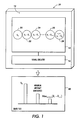
- Fig. 1 shows
article 10 withsubstrate 12 on the surface of which circuitry is formed. The circuitry includesarray 14 of light active units, a series of which is shown in greater detail. The circuitry also includes signal circuitry for receiving signals from or providing signals to light active units inarray 14. -
Array 14 includes a series of (n+1) lightactive units active unit 20, the largest in the series. Lightactive unit 22 is smaller than lightactive unit 20 by a first difference δ1, lightactive unit 24 is smaller by a second difference δ2, and so forth for other intermediate light active units in the series. Therefore, lightactive unit 26 is smaller by an (n-1)th difference δn-1 and the smallest, lightactive unit 28, is smaller by an nth difference δn. In general, δi>δi-1, so that the differences increase monotonically through the series, so that each intermediate unit in the series between lightactive units - Fig. 1 also shows
image size 30, the image size with whicharray 14 interacts. Withinimage size 30 is a bar graph with three bars representing key differences between effective sizes of adjacent light active units. The left bar represents the size difference δn, the difference that would occur if lightactive units image size 30 whenarticle 10 is in use. The right bar represents the maximum size difference between adjacent light active units in the series ofunits 20 through 28, abbreviated as Maxi=1 to n (δi-δi-1). As can be seen, δn>MAD>Maxi=1 to n (δi-δi-1). Therefore, despite the presence inarray 14 of lightactive units unit 20 tounit 28 have effective size differences insufficient to produce an artifact. - Fig. 2 shows
display array 50, withsubstrate 52 on a surface of whicharray circuitry 54 provides an array of light control units. The signal circuitry forarray circuitry 54 has a first set of lines extending left and right and a second set of lines extending up and down. The first set of lines could, for example, be scan lines, and the second set could be data lines. As shown, the signal circuitry includes pairedlines lines lines -
Region 60 ofarray circuitry 54 is shown in more detail at the right side of Fig. 2.Region 60 includes, in addition to paired left andright lines right lines lines Lines lines lines lines lines Lines - Because of the presence of paired
lines array circuitry 54. If there were no paired lines, the spacings between left and right lines could all take a maximum value of H, the spacing betweenlines - To a first approximation, the effective size of light control units in each row is proportional to the spacing between the lines immediately above and below that row, assuming that the up and down lines are all evenly spaced at the same spacing as
lines display array 50, it may be possible to make all the differences in spacing between adjacent rows less than the minimum artifact difference by slightly modifying the pitch of rows near pairedlines lines - As shown in Fig. 2, the spacing between
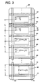
lines lines lines - The pitch changing approach in Fig. 2 could, however, result in line defect artifacts if it results in apertures that are not evenly spaced. Since the effective size of each light control unit depends on its aperture area, and since the effective position of each light control unit is the center of its aperture area, an even better approach may be to shape light control unit apertures while keeping pitch constant wherever possible, as illustrated in Fig. 3.
- Fig. 3 shows the same lines as in Fig. 2, and
aperture areas lines aperture areas aperture areas aperture areas Aperture areas lines aperture area 90 is spaced more fromline 62 than fromline 56, andaperture area 92 is similarly spaced more fromline 64 than fromline 58. -
Aperture area 94 has a height of h+ a1Δ, again divided equally above and below its center.Aperture area 96 has a height of h+a2Δ, again divided equally above and below its center. Andaperture area 98 has a height of H=h+ anΔ, also divided equally above and below its center. As a result of these heights, the same analysis applies to Fig. 3 as to Fig. 2: If ai=i, for example, then all the differences in spacing between adjacent rows are equal to Δ; if Δ is less than the minimum artifact difference, it is an insufficient difference to produce a perceptible artifact. More generally, if Δ is less than the minimum artifact difference and ai-ai-1≤1.0 for all values of i from 1 to n, each of the differences in spacing will be insufficient to produce a perceptible artifact. - The general features described above could be implemented using nearly any conventional AMLCD technology, but adding one or more repair structures within the array region so that a repair can be made as described above. The implementation described below can be made using AMLCD technology described in US-A-5 491 347.
- Figs. 4-6 show features of a layout of a split array.
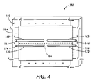
-
Display array 150 in Fig. 4 includessubstrate 152, which can be a transparent glass sheet as described in relation to Fig. 7 of US-A-5 491 347.Array region 154 on the surface ofsubstrate 152 is split into upper and lower array regions alongsplit line 156. 4096 scan lines, with signal leads s1 through s4096 on the left and with signal leads s'1 through s'4096 on the right, extend acrossarray region 154, with 2048 scan lines abovesplit line 156 and 2048 below. 6144 data lines, extend across each part ofarray region 154 with the data lines abovesplit line 156 having signal leads d1 through d6144 at the upper side and with the data lines belowsplit line 156 having signal leads d'1 through d'6144 at the lower side and with the data lines above and belowsplit line 156 collinear. - The circuitry in
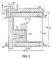
array region 154 also includes two repair structures. The upper repair stucture is along the upper side ofsplit line 156, and includesrepair lines array region 154 and connectingleads outside array region 154. The lower repair structure is along the lower side ofsplit line 156, and includesrepair lines array region 154 and connectingleads outside array region 154. - Fig. 5, which is a modified version of Fig. 3 of US-A-5 491 347, shows a layout for a light control unit. Fig. 5 shows several layers, with upper layers that are farthest from the substrate's surface obscuring lower layers. The uppermost layer shown in Fig. 5 is a top metal layer, which forms
data line 200 connected to a channel lead of an amorphous silicon (a-Si) transistor that switches the light control unit; the top metal layer also forms several other features described below. The next layer shown is a layer of indium-tin-oxide (ITO), which formstransparent electrode 202. The next layer is a top nitride layer, which forms insulatingisland 204, part of the transistor; the top nitride is an insulating layer that can form other features as mentioned below. The lowest layer shown is a bottom metal layer, which formsgate line 201,repair line 208, and, connected togate line 201,gate lead 210, which serves as the gate lead of the transistor. -
Data line 200 provides a data signal to a column of light control units, one of which is shown in Fig. 5. The part ofdata line 200 that extends overgate lead 210 connects to one channel lead of the transistor.Gate line 201 similarly provides a scan signal to a row of light control units. -
Data line 200 andgate line 201 are illustratively each 10 µm wide, andrepair line 208 can be of approximately the same width, as shown.Data line 200 crosses overgate line 201 incrossover region 220 and overrepair line 208 inrepair crossing region 222.Crossover region 220 andrepair crossing region 222 can each include an insulator formed by the top nitride layer and other features as necessary to ensure that the lines conduct signals adequately and that signals in the lines do not interfere. -
Transparent electrode 202 connects to the other channel lead of the transistor throughline 230, formed by the top metal layer. Therefore, when the transistor is conductive due to a scan signal provided to gate lead 210 bygate line 201,transparent electrode 202 receives and stores a drive signal fromdata line 200 throughline 230. -
Transparent electrode 202 also connects to charginglead 232, which implements one electrode of a storage capacitor and is formed by the top metal layer.Gate line 234. formed by the bottom metal layer, implements the other electrode of the storage capacitor;gate line 234 also provides a scan signal to the next light control unit in the same column. - The light control unit shown in Fig. 5 is square, and an array of identical light control units would have effective widths in the row and column directions of 90 µm × 90 µm.
- The patterned layers shown in Fig. 5 can be produced using the technique described in relation to Fig. 4 of US-A-5 491 347. The bottom metal pattern can include
repair line 208 and can also include peripheral lines that cross data lines outside the array region. - Fig. 6 shows part of the layout of the bottom metal pattern along
split line 156 in greater detail. Alongsplit line 156 arerepair lines repair lines scan lines - Each of the light control units could be laid out as illustrated in Fig. 5, with the rows above
split line 156 rotated 180°. In this case,scan lines split line 156, whilescan lines scan lines Scan lines scan lines scan lines scan lines scan lines - Alternatively, the light control units in the first rows along
split line 156 could be laid out with repair lines along the scan lines that drive the first rows, in which case scanlines scan lines scan lines - Fig. 6 shows sizes in the y-direction of rows of light control units between adjacent lines in the bottom metal pattern. The sizes shown can either indicate the actual spacing in the y-direction between adjacent lines or the aperture size in the y-direction that, when taken with the actual aperture size in the x-direction, would produce the actual aperture area of each light control unit between the lines. In either case, the sizes are such that a human viewer with normal vision
viewing display array 150 at usual viewing distances cannot perceive a difference between single lines such aslines lines - The size of the row of light control units between
adjacent lines adjacent lines lines split line 156 and n below. The rows next to splitline 156, referred to above as the first rows, have a size of (h MAX-δn), the smallest size shown. The second rows have a size of (h MAX-δn-1), the third rows (h MAX-δn-2), and so forth until the nth rows have a size of (h MAX-δ1). If the centers oflines split line 156 is the same as one line width. - The δi should increase monotonically from δ1 through δn. If the δi increase by equal increments Δ=δ1, then Σδi=(n2+n) Δ and we obtain δi =iΔ=(ih LINE)/(n2+n). For the layout of Fig. 5, h LINE=10µm and h MAX=80µm, so that if n=10, for example, then A=0.09µm, and the smallest size (h MAX-δn)=70.1µm. Although the difference between light control units of 80µm and light control units of 70.1µm might be perceptible if they were juxtaposed, when the transition between them is in increments of 0.09µm, perceptibility is decreased.
- On the other hand, if the minimum mask resolution is 0.5µm, the increments can be no smaller than 0.5µm. For the situation where increments are constrained by minimum mask resolution, it may be preferable to step the δi by equal increments Δ=δ1 after groups of rows, such as after each 10th row. In this and similar situations, larger values of n may be appropriate, such as n=100. This approach spreads the difference over a larger area, which may also decrease perceptibility.
- To avoid perceptible artifacts due to off-centered light control units, each single line or group of lines can be centered on the appropriate position and the apertures of the light control units can be adjusted.
- The approach of Fig. 6, with four lines grouped along
split line 156, may work best with light control units that have large aperture areas and are separated by relatively narrow lines, because the proportional difference between adjacent rows of light control units will be relatively small. For light control units separated by relatively wide lines, it may be preferable to move the repair line a row away fromsplit line 156, leaving three pairs of lines rather than a group of four lines, although this may result in some additional capacitance with the repair lines. - Figs. 7 and 8 show features of a structure laid out as described above. Fig. 7 shows a cross section along line B-B in Fig. 5. Fig. 8 shows a cross section along line C-C in Fig. 5. The cross sections in Figs. 7 and 8 can be understood more fully from US-
A-5 486 939. The structure shown in Figs. 7 and 8, which are similar respectively to Figs. 8 and 9 of US-A-5 486 939, can be produced using the process in Fig. 7 of US-A-5 486 939, which is substantially the same as Fig. 4 of US-A-5 491 347. Layers of the same material are similarly shaded and bear the same reference number in the two drawings. -
Substrate 300 hassurface 302 at which a thin-film structure is formed, beginning withbottom metal layer 304. Fig. 7 shows part ofbottom metal layer 304 inrepair line 208 in Fig. 5, while Fig. 8 showsrepair line 208 at right andscan line 234 at left. Overbottom metal layer 304 isbottom nitride layer 310, followed by undopedamorphous silicon layer 312. Overamorphous silicon layer 312 istop nitride layer 314. Overtop nitride layer 314 where it exists and overamorphous silicon layer 312 elsewhere is n+amorphous silicon layer 320. Overn+ layer 320 istop metal layer 322. Overtop metal layer 322 and other exposed layers can be a passivation layer (not shown). - Additional features of the structure in Figs. 7 and 8 can be understood from the description in US-
A-5 486 939. - Figs. 9 and 10 show features of repair techniques.
- The act in
box 350 in Fig. 9 begins by producing a split array that includes repair lines that are parallel to scan lines and that cross data lines. The act inbox 350 can be implemented as described above in relation to Figs. 4-6. - The act in
box 352 then tests the split array for data line defects. Since each data line has only one accessible lead, this cannot be done with conventional continuity testing. Instead, test equipment such as the In-Process Tester (IPT) from Photon Dynamics, Inc., Milpitas, California can be used to find defects in the array. As explained by Bond, J., and Levenson, M.D., "The US gears up to challenge Japan in flat panel displays," Solid State Technology, December 1993, pp. 37, 38, and 40-43, the IPT can use a noncontact method of performing voltage imaging on AMLCDs before cell assembly. The IPT can scan the substrate with light to collect data on the location and type of line defects, testing all the data lines. - The act in
box 354 repairs data line shorts by laser cutting to eliminate each short. This act may include cutting a data line to create an open on each side of a short to a scan line, for example. This act can be performed with the Photon Dynamics LCD Panel Repair System using the integrated laser trim (ILT) capability. - The act in
box 360 repairs data line opens, including any created inbox 354, by laser welding each open data line to a repair line that it crosses and to a peripheral line that it crosses. This act can also be performed with the Photon Dynamics LCD Panel Repair System, but using the integrated laser weld (ILW) capability to produce conductive paths between lines that cross. - The act in
box 362 then assembles an LCD in the manner described in the Dense Array and Crossing Lines Patents, but with TABs as described above connecting leads on the split array to drive circuitry on PCBs around the edge of the split array. Because each data line in each part of the split array must be driven, data drivers cannot be interdigitated with alternate data lines driven from opposite ends. Instead, each data line must be driven, both from the top and from the bottom of the split array. Therefore, data drivers must be on 90µm pitch, which may be achieved with overlapping TAB drivers or fine pitch TABs. Data drive circuitry may also be connected using techniques like those described inEP Application Number 96 303 897.1. - The act in
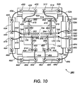
box 364 completes repair of data line opens by soldering wires for each open data line so that one or more highly conductive lines on the PCBs are electrically connected between the connecting lead of the data line's repair line and the lead of the data line's peripheral line. - Fig. 10 shows features of a repaired
array 380 produced by the technique of Fig. 9 usingarray 150 in Fig. 4. witharray region 154 on a surface ofsubstrate 152. and withrepair lines 160. 162, 170, and 172 having connectingleads substrate 152 by TABs as in Figs. 1 and 8. -
Open lines lines laser welds Open lines peripheral lines laser welds - Lead 420 on peripheral line 400 is electrically connected to lead 422 on
conductive line 424 bywire 426. Lead 430 onconductive line 424 is in turn connected to lead 432 onconductive line 434 bywire 436. Lead 440 onconductive line 434 is in turn connected to connectinglead 164 bywire 442, completing the repair ofopen line 382. - Lead 450 on
peripheral line 404 is electrically connected to lead 452 onconductive line 454 bywire 456. Lead 460 onconductive line 454 is in turn connected to lead 462 onconductive line 464 bywire 466. Lead 470 onconductive line 464 is in turn connected to connectinglead 174 bywire 472, completing the repair ofopen line 386. - Lead 480 on
peripheral line 406 is electrically connected to lead 482 onconductive line 484 bywire 486. Lead 490 onconductive line 484 is in turn connected to lead 492 onconductive line 494 bywire 496. Lead 500 onconductive line 494 is in turn connected to connecting lead 676 bywire 502, completing the repair ofopen line 388. - Lead 510 on
peripheral line 402 is electrically connected to lead 512 onconductive line 514 bywire 516. Lead 520 onconductive line 514 is in turn connected to lead 522 onconductive line 524 bywire 526. Lead 530 onconductive line 524 is in turn connected to connecting lead 666 bywire 532, completing the repair ofopen line 384. - The above implementation provides an array appropriate for an AMLCD, but the invention could be implemented in another type of display array, in another type of light valve array, or in another array in which light active units interact with images.
- The above implementation provides an array of cells with particular dimensions and densities. The invention could be implemented with a wide variety of array sizes and shapes, cell sizes and shapes, and cell densities.
- The above implementation adjusts sizes of cells due to a group of four lines. The invention could provide appropriately sized light active units in various other situations, including situations in which lines are paired or in which a light active unit's effective size is reduced by a line that crosses the center of the unit.
- The above implementation provides a split array with four repair lines along the split. The invention could be implemented, however, with an array that is not split or with an array with more or less repair lines or with repair lines positioned elsewhere within an array.
- The above implementation eliminates artifacts resulting from grouped lines that cross data lines, but the invention could be implemented to eliminate artifacts from grouped lines that cross scan lines.
- The above implementation provides an active matrix array, but the invention could also be implemented in a passive matrix array.
- The above implementation uses particular materials in a thin-film structure, but other materials could be used in other types of structures to implement the invention. Some examples are discussed in US-A-5 491 347. For example, an array could be implemented with polysilicon TFTs rather than amorphous silicon TFTs, and some of the drive circuitry could be integrated on the same substrate as the array. Rather than metal lines, the data lines and scan lines could include other conductive materials such as doped semiconductive material. Rather than silicon nitride, the insulating layers could include other insulating materials.
- The implementation described above provides thin film circuitry on an insulating substrate. The invention could be implemented with other types of circuitry on other types of substrates.
- The above implementations use particular processes to produce a thin-film structure, but other processes could be used.
- The implementation described above provides circuitry with specific geometric characteristics, but the invention could be implemented with different geometries.
- The above implementation uses a specific layout for each cell in an array, but other layouts could be used, including a layout in which a repair line is along the opposite side of the cell,as mentioned above in relation to Fig. 6.
- The implementation described above includes layers in a specific sequence, but the sequence of layers could be modified, such as by producing a top gate TFT structure or a structure in which scan lines cross over data lines.
- The invention could be applied in many ways, including elimination of artifacts in display arrays, light valve arrays, and other arrays that interact with images.
- The invention has been described in relation to thin-film implementations, but the invention might be implemented with single crystal technology.
Claims (10)
- An article (10; 50; 150; 380) comprising:a substrate (12; 52;152) with a surface at which circuitry can be formed;array circuitry formed at the surface of the substrate, the array circuitry comprising:an array (14; 54) of light active units (20-28); each light active unit having an effective size (S1...S2); the array of light active units together interacting with images having an image size (30); andsignal circuitry (16) for receiving signals from or providing signals to the light active units;the array of light active units including:a first light active unit (20) that has a first effective size (S1);a second light active unit (28) that has second effective size (S2) smaller than the first effective size by an overall size difference (δn); the overall size difference being sufficient to produce an artifact in images having the image size if the first and second light active units were adjacent to each other; the first and second light active units being separated in the array by a spacing; anda subarray of intermediate light active units (22, 24, 26) in the spacing that form a series of light active units extending from the first light active unit to the second light active unit; each intermediate light active unit having an effective size less than the effective size of the light active unit preceding it in the series by a first size difference and greater than the effective size of the light active unit following it in the series by a second size difference; the first and second size differences of each intermediate light active unit being insufficient to produce an artifact in images having the image size.
- The article of claim 1 in which the signal circuitry comprises:a first set of lines (200) extending across the surface of the substrate;a second set of lines (201, 208) extending across the surface of the substrate so that each of the first set of lines and each of the second set of lines cross in a crossing region (220);each light active unit being electrically connected to one of the first set of lines and one of the second set of lines and adjacent the crossing region of the lines to which it is electrically connected.
- The article of claim 1 or claim 2 in which the article is a display; each light active unit being a light control unit (Fig.5) for causing presentation of a segment of images.
- The article of claim 3 in which each light control unit has an aperture within which the light control unit causes presentation of its segment; the effective size of each light control unit being an area of its aperture (90, 92, 94, 96, 98).
- The article of claim 4 in which each light control unit has an effective center of its aperture; the effective centers of the light control units in the series being evenly spaced (L).
- The article of claim 4 in which the series extends in a first direction; each light control unit's aperture having a transverse size in a second direction perpendicular to the first direction; the transverse size of all the light control units in the series being substantially equal.
- The article of claim 1 in which the article is a display; the array circuitry further comprising:scan lines (201, 208) extending in a first direction; anddata lines (200) extending in a second direction approximately perpendicular to the first direction so that each data line crosses a scan line in a crossing area;each light active unit being a light control unit;each light control unit being electrically connected to one of the scan lines (201) and one of the data lines (200) so that the light control unit receives signals from its data line under control of signals from its scan line; each light control unit responding to signals from its scan line and its data line by causing presentation of a segment of images; each light control unit having an effective aperture area (90, 92, 94, 96, 98), the light control unit's effective aperture area being the effective area of image segments presented by the light control unit; each scan line providing signals to a row of the light control units; each data line providing signals to a column of the light control units; the array of light control units together presenting images having the image size;a first column of the light control units including the first and second light active units and the subarray of intermediate light active units:the first light active unit being a first light control unit that has a first effective aperture area (98);the second light active unit being a second light control unit that has a second effective aperture area (92) smaller than the first effective aperture area by the overall size difference; the first and second light control units being separated in the column by the spacing; andthe subarray of intermediate light active units being one or more intermediate light control units in the spacing that form a series of light control units extending from the first light control unit to the second light control unit; each intermediate light control unit having an effective aperture area (94,96) less than the effective aperture area of the light control unit preceding it in the series by the first size difference and greater than the effective aperture area of the light control unit following it in the series by the second size difference.
- The article of claim 7 in which each light control unit's effective aperture area is bounded by lines extending in the first direction, each light control unit's bounding lines being separated by a spacing; the spacing of the first light control unit's bounding lines being greater than the spacing of the second light control unit's bounding lines by the overall size difference; the spacing of each intermediate light control unit's bounding lines being less than the spacing of the bounding lines of the light control unit preceding it in the series by the first size difference and greater than the spacing of the bounding lines of the light control unit following it in the series by the second size difference.
- The article of claim 7, further comprising a dark matrix that defines, for each light control unit, an aperture boundary that has a size in the second direction; the size in the second direction of the first light control unit's aperture boundary being greater than the size in the second direction of the second light control unit's aperture boundary by the overall size difference; the size in the second direction of each intermediate light control unit's aperture boundary being less than the size in the second direction of the aperture boundary of the light control unit preceding it in the series by the first size difference and greater than the size in the second direction of the aperture boundary of the light control unit following it in the series by the second size difference.
- The article of claim 7, claim 8 or claim 9 in which the array circuitry further comprises a repair line (250, 252) parallel to and alongside a first one of the scan lines (254, 256); the second light control unit being along the first scan line.
Applications Claiming Priority (2)
| Application Number | Priority Date | Filing Date | Title |
|---|---|---|---|
| US579048 | 1990-09-07 | ||
| US08/579,048 US5731803A (en) | 1995-12-21 | 1995-12-21 | Array with light active units sized to eliminate artifact from size difference |
Publications (3)
| Publication Number | Publication Date |
|---|---|
| EP0780904A2 true EP0780904A2 (en) | 1997-06-25 |
| EP0780904A3 EP0780904A3 (en) | 1999-08-11 |
| EP0780904B1 EP0780904B1 (en) | 2009-02-18 |
Family
ID=24315372
Family Applications (1)
| Application Number | Title | Priority Date | Filing Date |
|---|---|---|---|
| EP96309251A Expired - Lifetime EP0780904B1 (en) | 1995-12-21 | 1996-12-18 | Pixel matrix display whose geometry allows for the suppression of image artifacts due to discontinuities in the pixel array |
Country Status (4)
| Country | Link |
|---|---|
| US (1) | US5731803A (en) |
| EP (1) | EP0780904B1 (en) |
| JP (1) | JPH09230386A (en) |
| DE (1) | DE69637835D1 (en) |
Families Citing this family (3)
| Publication number | Priority date | Publication date | Assignee | Title |
|---|---|---|---|---|
| TWI223713B (en) * | 2003-03-31 | 2004-11-11 | Toppoly Optoelectronics Corp | Method and system for testing driver circuits of AMOLED |
| US8228350B2 (en) * | 2008-06-06 | 2012-07-24 | Omnivision Technologies, Inc. | Data dependent drive scheme and display |
| US10926357B2 (en) * | 2017-04-12 | 2021-02-23 | Dpix, Llc | Method and functional architecture for inline repair of defective imaging arrays |
Citations (3)
| Publication number | Priority date | Publication date | Assignee | Title |
|---|---|---|---|---|
| US5464984A (en) | 1985-12-11 | 1995-11-07 | General Imaging Corporation | X-ray imaging system and solid state detector therefor |
| US5486939A (en) | 1994-04-28 | 1996-01-23 | Xerox Corporation | Thin-film structure with insulating and smoothing layers between crossing conductive lines |
| US5491347A (en) | 1994-04-28 | 1996-02-13 | Xerox Corporation | Thin-film structure with dense array of binary control units for presenting images |
Family Cites Families (19)
| Publication number | Priority date | Publication date | Assignee | Title |
|---|---|---|---|---|
| JPS60218626A (en) * | 1984-04-13 | 1985-11-01 | Sharp Corp | Color llquid crystal display device |
| US5602679A (en) * | 1987-12-31 | 1997-02-11 | Projectavision, Inc. | High efficiency light valve projection system |
| JPH0823643B2 (en) * | 1989-03-28 | 1996-03-06 | シャープ株式会社 | Active matrix display |
| DE3910418A1 (en) * | 1989-03-31 | 1990-10-04 | Licentia Gmbh | DISPLAY DEVICE |
| DE69013239T2 (en) * | 1989-06-20 | 1995-05-04 | Sharp Kk | Matrix display device. |
| JPH03107189A (en) * | 1989-09-20 | 1991-05-07 | Matsushita Electric Ind Co Ltd | Display device |
| CA2075441A1 (en) * | 1991-12-10 | 1993-06-11 | David D. Lee | Am tft lcd universal controller |
| JP3206976B2 (en) * | 1992-07-28 | 2001-09-10 | 京セラ株式会社 | Liquid crystal display device |
| CN1065051C (en) * | 1992-08-13 | 2001-04-25 | 卡西欧计算机公司 | Thin-film transistor array and liquid crystal display device using the thin-film transistor array |
| JPH06282245A (en) * | 1993-03-25 | 1994-10-07 | Toshiba Corp | Image display device and image processing system |
| DE69409453T2 (en) * | 1993-08-31 | 1998-11-12 | Advanced Micro Devices Inc | Device for changing an electrical signal |
| US5485293A (en) * | 1993-09-29 | 1996-01-16 | Honeywell Inc. | Liquid crystal display including color triads with split pixels |
| US5475246A (en) * | 1993-12-20 | 1995-12-12 | General Electric Company | Repair line structure for thin film electronic devices |
| WO1995017768A1 (en) * | 1993-12-20 | 1995-06-29 | General Electronic Company | Address line repair structure and method for thin film imager devices |
| US5381014B1 (en) * | 1993-12-29 | 1997-06-10 | Du Pont | Large area x-ray imager and method of fabrication |
| JPH09511616A (en) * | 1994-03-31 | 1997-11-18 | イメイション・コーポレイション | Imaging system with variable electrode arrangement and processing |
| US5473452A (en) * | 1994-12-21 | 1995-12-05 | Goldstar Co., Ltd. | Liquid crystal display device with repair structure |
| US5648674A (en) * | 1995-06-07 | 1997-07-15 | Xerox Corporation | Array circuitry with conductive lines, contact leads, and storage capacitor electrode all formed in layer that includes highly conductive metal |
| US5608245A (en) * | 1995-12-21 | 1997-03-04 | Xerox Corporation | Array on substrate with repair line crossing lines in the array |
-
1995
- 1995-12-21 US US08/579,048 patent/US5731803A/en not_active Expired - Lifetime
-
1996
- 1996-11-28 JP JP8318145A patent/JPH09230386A/en active Pending
- 1996-12-18 EP EP96309251A patent/EP0780904B1/en not_active Expired - Lifetime
- 1996-12-18 DE DE69637835T patent/DE69637835D1/en not_active Expired - Lifetime
Patent Citations (3)
| Publication number | Priority date | Publication date | Assignee | Title |
|---|---|---|---|---|
| US5464984A (en) | 1985-12-11 | 1995-11-07 | General Imaging Corporation | X-ray imaging system and solid state detector therefor |
| US5486939A (en) | 1994-04-28 | 1996-01-23 | Xerox Corporation | Thin-film structure with insulating and smoothing layers between crossing conductive lines |
| US5491347A (en) | 1994-04-28 | 1996-02-13 | Xerox Corporation | Thin-film structure with dense array of binary control units for presenting images |
Non-Patent Citations (1)
| Title |
|---|
| BOND J., LEVENSON M.D.: "The US gears up to challenge Japan in flat panel displays.", SOLID STATE TECHNOLOGY., December 1993 (1993-12-01), pages 37/38 - 40-43 |
Also Published As
| Publication number | Publication date |
|---|---|
| US5731803A (en) | 1998-03-24 |
| EP0780904B1 (en) | 2009-02-18 |
| JPH09230386A (en) | 1997-09-05 |
| DE69637835D1 (en) | 2009-04-02 |
| EP0780904A3 (en) | 1999-08-11 |
Similar Documents
| Publication | Publication Date | Title |
|---|---|---|
| US6111621A (en) | Flat panel display devices having improved signal line repair capability | |
| KR100997965B1 (en) | Liquid crystal display | |
| KR100806897B1 (en) | a thin film transistor array for a liquid crystal display | |
| US6982569B2 (en) | Multiple testing bars for testing liquid crystal display and method thereof | |
| KR100298995B1 (en) | Liquid Crystal Display and Inspection Method | |
| US5517341A (en) | Liquid crystal display with TFT and capacitor electrodes with redundant connection | |
| US6172729B1 (en) | Liquid crystal display device of delta arrangement having pixel openings with sides oblique to scan lines | |
| US6052167A (en) | Liquid crystal display having only one common line in peripheral region of substrate | |
| EP1672414B1 (en) | Thin film transistor array panel and liquid crystal display including the panel | |
| CN101364395B (en) | Display device and driving method thereof | |
| EP0780766B1 (en) | Array on substrate and producing method therefor | |
| US20060262251A1 (en) | Four color liquid crystal display | |
| US20160035271A1 (en) | Display device and driving method thereof | |
| USRE39798E1 (en) | Active matrix LCD device with image signal lines having a multilayered structure | |
| TWI398712B (en) | Thin film transistor array panel with improved connection to test lines | |
| US20050231534A1 (en) | Apparatus and method for driving a display device | |
| US20040109099A1 (en) | Thin film transistor array panel for liquid crystal display | |
| US6226057B1 (en) | Liquid crystal display having overlapped pixel electrodes and method for fabricating the same | |
| US20080180372A1 (en) | Display device | |
| JP2007114778A (en) | Thin film transistor display plate | |
| KR20030054280A (en) | a liquid crystal display | |
| US8339534B2 (en) | Display device | |
| JPH11133887A (en) | Color display device | |
| GB2275809A (en) | Liquid crystal display | |
| US20120194414A1 (en) | Liquid crystal display |
Legal Events
| Date | Code | Title | Description |
|---|---|---|---|
| PUAI | Public reference made under article 153(3) epc to a published international application that has entered the european phase |
Free format text: ORIGINAL CODE: 0009012 |
|
| AK | Designated contracting states |
Kind code of ref document: A2 Designated state(s): DE FR GB |
|
| PUAL | Search report despatched |
Free format text: ORIGINAL CODE: 0009013 |
|
| AK | Designated contracting states |
Kind code of ref document: A3 Designated state(s): DE FR GB |
|
| RIC1 | Information provided on ipc code assigned before grant |
Free format text: 6G 02F 1/1343 A, 6G 02F 1/136 B, 6H 01L 27/146 B |
|
| 17P | Request for examination filed |
Effective date: 20000211 |
|
| 17Q | First examination report despatched |
Effective date: 20040211 |
|
| 17Q | First examination report despatched |
Effective date: 20040211 |
|
| GRAP | Despatch of communication of intention to grant a patent |
Free format text: ORIGINAL CODE: EPIDOSNIGR1 |
|
| RTI1 | Title (correction) |
Free format text: PIXEL GEOMETRY FOR THE SUPPRESSION OF IMAGE ARTIFACTS DUE TO DISCONTINUITIES IN THE PIXEL ARRAY OF A DISPLAY |
|
| RTI1 | Title (correction) |
Free format text: PIXEL MATRIX DISPLAY WHOSE GEOMETRY ALLOWS FOR THE SUPPRESSION OF IMAGE ARTIFACTS DUE TO DISCONTINUITIES IN THE PIXEL ARRAY |
|
| GRAS | Grant fee paid |
Free format text: ORIGINAL CODE: EPIDOSNIGR3 |
|
| RAP1 | Party data changed (applicant data changed or rights of an application transferred) |
Owner name: THOMSON LICENSING LLC |
|
| GRAA | (expected) grant |
Free format text: ORIGINAL CODE: 0009210 |
|
| AK | Designated contracting states |
Kind code of ref document: B1 Designated state(s): DE FR GB |
|
| REG | Reference to a national code |
Ref country code: GB Ref legal event code: FG4D |
|
| REF | Corresponds to: |
Ref document number: 69637835 Country of ref document: DE Date of ref document: 20090402 Kind code of ref document: P |
|
| PLBE | No opposition filed within time limit |
Free format text: ORIGINAL CODE: 0009261 |
|
| STAA | Information on the status of an ep patent application or granted ep patent |
Free format text: STATUS: NO OPPOSITION FILED WITHIN TIME LIMIT |
|
| 26N | No opposition filed |
Effective date: 20091119 |
|
| PGFP | Annual fee paid to national office [announced via postgrant information from national office to epo] |
Ref country code: GB Payment date: 20121219 Year of fee payment: 17 |
|
| PGFP | Annual fee paid to national office [announced via postgrant information from national office to epo] |
Ref country code: DE Payment date: 20121217 Year of fee payment: 17 Ref country code: FR Payment date: 20130128 Year of fee payment: 17 |
|
| REG | Reference to a national code |
Ref country code: DE Ref legal event code: R119 Ref document number: 69637835 Country of ref document: DE |
|
| GBPC | Gb: european patent ceased through non-payment of renewal fee |
Effective date: 20131218 |
|
| REG | Reference to a national code |
Ref country code: FR Ref legal event code: ST Effective date: 20140829 |
|
| REG | Reference to a national code |
Ref country code: DE Ref legal event code: R119 Ref document number: 69637835 Country of ref document: DE Effective date: 20140701 |
|
| PG25 | Lapsed in a contracting state [announced via postgrant information from national office to epo] |
Ref country code: DE Free format text: LAPSE BECAUSE OF NON-PAYMENT OF DUE FEES Effective date: 20140701 |
|
| PG25 | Lapsed in a contracting state [announced via postgrant information from national office to epo] |
Ref country code: FR Free format text: LAPSE BECAUSE OF NON-PAYMENT OF DUE FEES Effective date: 20131231 Ref country code: GB Free format text: LAPSE BECAUSE OF NON-PAYMENT OF DUE FEES Effective date: 20131218 |