EP0782077A1 - Method and arrangement for converting memory addresses into memory control signals - Google Patents
Method and arrangement for converting memory addresses into memory control signals Download PDFInfo
- Publication number
- EP0782077A1 EP0782077A1 EP96119487A EP96119487A EP0782077A1 EP 0782077 A1 EP0782077 A1 EP 0782077A1 EP 96119487 A EP96119487 A EP 96119487A EP 96119487 A EP96119487 A EP 96119487A EP 0782077 A1 EP0782077 A1 EP 0782077A1
- Authority
- EP
- European Patent Office
- Prior art keywords
- memory
- capacity
- information
- logical
- configuration information
- Prior art date
- Legal status (The legal status is an assumption and is not a legal conclusion. Google has not performed a legal analysis and makes no representation as to the accuracy of the status listed.)
- Granted
Links
Images


Classifications
-
- G—PHYSICS
- G06—COMPUTING; CALCULATING OR COUNTING
- G06F—ELECTRIC DIGITAL DATA PROCESSING
- G06F12/00—Accessing, addressing or allocating within memory systems or architectures
- G06F12/02—Addressing or allocation; Relocation
- G06F12/06—Addressing a physical block of locations, e.g. base addressing, module addressing, memory dedication
- G06F12/0646—Configuration or reconfiguration
- G06F12/0684—Configuration or reconfiguration with feedback, e.g. presence or absence of unit detected by addressing, overflow detection
-
- G—PHYSICS
- G06—COMPUTING; CALCULATING OR COUNTING
- G06F—ELECTRIC DIGITAL DATA PROCESSING
- G06F12/00—Accessing, addressing or allocating within memory systems or architectures
- G06F12/02—Addressing or allocation; Relocation
- G06F12/06—Addressing a physical block of locations, e.g. base addressing, module addressing, memory dedication
- G06F12/0646—Configuration or reconfiguration
- G06F12/0653—Configuration or reconfiguration with centralised address assignment
Abstract
Description
In prozessorgesteuerten Einrichtungen ist für die Speicherung von Programmen und Daten ein Speicher - üblicherweise dynamische oder statische RAM's (Random Access Memory) - vorgesehen. Um Daten in Speicherbereiche des Speichers zu schreiben oder Daten aus den einzelnen Speicherbereichen zu lesen, generiert der Prozessor eine Speicherbereichsadresse und übergibt diese an eine Speicheransteuerung - in der Fachwelt als SRAM- oder DRAM-Controller bekannt. Die Speicheransteuerung leitet diese Speicherbereichsadresse über Adreßleitungen an Adreßeingänge des Speichers weiter. Die Speicherbereichsadressen repräsentieren meist eine Dualzahl, wobei der kleinste adressierbare Speicherbereich üblicherweise ein oder mehrere Byte umfaßt.In processor-controlled devices, a memory - usually dynamic or static RAM's (Random Access Memory) - is provided for storing programs and data. In order to write data into memory areas of the memory or to read data from the individual memory areas, the processor generates a memory area address and transfers it to a memory controller - known in the art as SRAM or DRAM controller. The memory controller forwards this memory area address via address lines to address inputs of the memory. The memory area addresses usually represent a dual number, the smallest addressable memory area usually comprising one or more bytes.
Der Speicher ist durch mehrere Einsetzbereiche gebildet, in die jeweils zumindest ein Speichermodul - üblicherweise ein integrierter Speicherbaustein - eingesetzt werden kann. Die durch Steckeinrichtungen realisierten Einsetzbereiche sind häufig derart ausgestaltet, daß Speichermodule bzw. Speicherbausteine mit unterschiedlichen Speicherkapazitäten eingesetzt werden können - beispielsweise Speichermodule mit 1 oder 4 Kbyte bzw. Mbyte. Durch eine unterschiedliche Bestükkung der Einsetzbereiche ist folglich eine optimale Anpassung der Speicherkapazität des Speichers an die jeweilige Anwendung möglich. Dies bedeutet, daß die Speichermodule in Abhängigkeit von ihrer Speicherkapazität in die adressen-konformen Einsetzbereiche eingesetzt werden müssen, um eine fehlerfreie Speicheradressierung zu gewährleisten. Eine Fehlbestückung hinsichtlich der Speicherkapazität und der Einsetzbereiche führt zur erheblichen Störungen des Prozessorsystems bzw. zu dessen Ausfall.The memory is formed by a plurality of insertion areas, in each of which at least one memory module - usually an integrated memory module - can be inserted. The application areas realized by plug-in devices are often designed in such a way that memory modules or memory modules with different memory capacities can be used - for example memory modules with 1 or 4 Kbytes or Mbytes. By fitting the application areas differently, an optimal adaptation of the storage capacity of the memory to the respective application is possible. This means that the memory modules, depending on their memory capacity, have to be inserted in the address-conforming application areas in order to ensure error-free memory addressing. Incorrect loading of the memory capacity and the application areas leads to considerable malfunctions of the processor system or to its failure.
Die der Erfindung zugrundeliegende Aufgabe besteht darin, ausgehend von der durch den Prozessor generierten Speicherbereichsadresse unter Berücksichtigung einer flexiblen Konfiguration des Speicher eine Speicherkonfigurations-gerechte Adressierung des Speichers zu gewährleisten. Die Aufgabe wird durch die Merkmale des Anspruchs 1 gelöst.The object on which the invention is based is to ensure addressing of the memory in accordance with the memory configuration, starting from the memory area address generated by the processor, taking into account a flexible configuration of the memory. The object is solved by the features of
Der wesentliche Aspekt des erfindungsgemäßen Verfahren ist in der Bildung von Konvertierungsinformationen zu sehen, mit deren Hilfe die vom Prozessor generierten Speicherbereichsadressen in auf die aktuelle Speicherkonfiguration abgestimmte Speicheransteuersignale konvertiert werden. Hierbei werden jeweils jedem eingesetzten Speichermodul zugeordnete und eine die Speicherkapazität der jeweiligen Speichermodule anzeigende Kapazitätsinformationen und das Vorhandensein von eingesetzten Speichermodulen anzeigende Konfigurationsinformationen aller Einsetzbereiche erfaßt und aus den erfaßten Kapazitätsinformationen und den Konfigurationsinformationen in Abhängigkeit von den erfaßten Konfigurationsinformation den Adreßraum anzeigende logische Kapazitätsinformationen und die virtuelle Konfiguration des Speichers anzeigende, logische Konfigurationsinformationen abgeleitet. Die logischen Kapazitäts-informationen repräsentieren zuammen mit den Konfigurationsinformationen die Konvertierungsinformationen.The essential aspect of the method according to the invention can be seen in the formation of conversion information, with the aid of which the memory area addresses generated by the processor are converted into memory control signals which are matched to the current memory configuration. In this case, each of the memory modules assigned and information about the capacity indicating the memory capacity of the respective memory modules and the presence of memory modules used are detected configuration information of all application areas and from the detected capacity information and the configuration information as a function of the detected configuration information indicating the address space logical capacity information and the virtual configuration of the logical configuration information indicating the memory. The logical capacity information together with the configuration information represent the conversion information.
Bei einer m-stelligen, binären Speicherbereichsadresse sind n höchstwertige Stellen für die Konfiguration von 2n Einsetzbereichen vorgesehen, wobei in jeden Einsetzbereich Speichermodule mit einer Gesamtspeicherkapazität von 2m-n adressierbaren Speicherbereichen einsetzbar sind und für jeden Einsetzbereich wird eine Kapazitäts- und eine Konfigurationsinformation erfaßt - Anspruch 2. Durch diese Aufteilung werden Speichermodule mit 2x - Seicherkapazitätsabstufungen berücksichtigt. Andere Speicherkapazitätsabstufungen sind möglich, führen jedoch zu Adressierungseinschränkungen und zu erhöhten Aufwendungen für eine Realisierung des erfindungsgemäßen Verfahren.With an m-digit, binary memory area address, n most significant digits are provided for the configuration of 2 n application areas, memory modules with a total memory capacity of 2 mn addressable memory areas can be used in each application area, and capacity and configuration information are recorded for each
Gemäß einer vorteilhaften Weiterbildung des erfindungsgemäßen Verfahrens sind Speichermodule mit zwei unterschiedlichen Speicherkapazitäten einsetzbar, wobei die größere Speicherkapazität 2m-n adressierbare Speicherbereiche und die kleinere Speicherkapazität 2m-n-k (k,l,m,n = 1,2..) adressierbare Speicherbereiche umfaßt. Die Speichermodule mit der größeren Speicherkapazität werden, beginnend mit dem Einsetzbereich mit den kleinsten, zugeordneten Speicherbereichsadressen, sukzessive in die Einsetzbereiche mit den nächst höherwertigeren zugeordneten Speicherbereichsadressen eingesetzt. Die erfaßten Kapazitätsinformationen sind durch eine die kleine oder große Speicherkapazität anzeigende, binäre Kapazitätsinformation und die Konfigurationsinformation durch eine das Vorhandensein oder nicht Vorhandensein eines eingesetzten Speichermoduls anzeigende, binäre Konfigurationsinformation repräsentiert - Anspruch 3. Durch diese Einschränkung, die zwar Fehlbestückungen erlaubt, wird jedoch die Speicherkapazität der fehlbestückten Speichermodule reduziert. Des weiteren kann durch die Einschränkung eine Konvertierungseinrichtung noch einfacher, d.h. wirtschaftlicher realisiert werden.According to an advantageous development of the method according to the invention, memory modules with two different memory capacities can be used, the
Ein weiterer erfindungswesentlicher Aspekt ist in der Benutzung der Konvertierungsinformationen zum Konvertieren von durch eine prozessorgesteuerte Einrichtung gebildeten Speicherbereichsadressen in auf eine Struktur und Speicherkapazität eines Speichers abgestimmte Speicheransteuersignale zu sehen, wobei der Speicher durch einheitliche und/oder unterschiedliche Speicherkapazitäten aufweisende Speichermodule gebildet ist, die jeweils in einen physikalischen Einseztbereich eingesetzt sind. Hierzu wird aus n+k, die Konfiguration des Speichers betreffende Stellen einer aktuell vorliegenden m-stelligen Speicherbereichsadresse mit Hilfe von aus die Speicherkapazität anzeigenden Kapazitätsinformationen abgeleiteten logischen Kapazitätsinformationen und aus von die virtuelle Speicherkonfiguration anzeigenden Konfigurationsinformationen abgeleiteten logischen Konfigurationsinformationen ein einsetzbereichsbezogenes logisches Speicheransteuersignal abgeleitet, und mit Hilfe der Konfigurationsinformationen wird aus dem einsetzbereichsbezogenen logischen Speicheransteuersignal für den betroffenen Einsetzbereich ein physikalisches Speicheransteuersignal abgeleitet.Another aspect essential to the invention can be seen in the use of the conversion information for converting memory area addresses formed by a processor-controlled device into memory drive signals matched to a structure and memory capacity of a memory, the memory being formed by memory modules having uniform and / or different memory capacities, each in a physical area of application are used. For this purpose, n + k, locations of the current m-digit memory area address relating to the configuration of the memory with the aid of logical capacity information derived from capacity information indicating the memory capacity and logical configuration information derived from the configuration information indicating the virtual memory configuration, becomes an application area-related logic memory drive signal and with the help of the configuration information, a physical memory control signal is derived from the application-related logical memory control signal for the application area concerned.
Weitere vorteilhafte Ausgestaltungen der erfindungsgemäßen Verfahrens sowohl zum Bilden von Konvertierungsinformationen als auch zum Konvertieren der Speicherbereichsadresse in Speicheransteuersigale sowie Anordnungen zur Durchführung der erfindungsgemäßen Verfahren sind den weiteren Ansprüchen zu entnehmen.Further advantageous refinements of the method according to the invention both for forming conversion information and for converting the memory area address into memory control signals and arrangements for carrying out the method according to the invention can be found in the further claims.
Die Erfindung wird im folgenden anhand von zeichnerischen Darstellungen näher erläutert. Dabei zeigen
- FIG 1
- eine Konfiguration eines Speichers mit der erfindungsgemäßen Konvertierungseinrichtung,
- FIG 2
- ein Blockschaltbild der Konvertierungseinrichtung,
- FIG 3
- die erste Verschiebestufe zur Bildung der logischen Kapazitäts- und Konfigurationsinformationen,
- FIG 4
- eine Kapazitätskorrekturstufe zum Bilden von Korrekturinformationen,
- FIG 5
- in einem Blockschaltbild eine Modulauswahleinheit
- FIG 6
- zum Bilden von logischen Speicheransteuersignalen und
- FIG 7
- eine zweite Verschiebestufe zur Bildung von physikalischen Speicheransteuersignalen.
- FIG. 1
- a configuration of a memory with the conversion device according to the invention,
- FIG 2
- a block diagram of the conversion device,
- FIG 3
- the first shift stage for the formation of the logical capacity and configuration information,
- FIG 4
- a capacity correction stage for forming correction information,
- FIG 5
- a module selection unit in a block diagram
- FIG 6
- for forming logical memory drive signals and
- FIG 7
- a second shift stage for the formation of physical memory drive signals.
FIG 1 zeigt eine für das Ausführungsbeispiel angenommene Konfiguration eines Speichers SP, der durch vier Einsetzbereiche EB1..4 gebildet ist, d.h. n = 2. In diese meist durch Steckplätze realisierte Einsetzbereiche EB1..4 sind jeweils Speichermodule SM mit einer vorgegebenen Speicherkapazität K1 oder der vierfachen vorgegebenen Speicherkapazität K4 einsetzbar bzw. steckbar - d.h. k = 2 -, wobei die vorgegebene Speicherkapazität K1 beispielsweise 1 MByte beträgt. Von den für eine Adressierung erforderlichen 24 - d.h. m = 24 - Adreßleitungen ADL sind n+k, im Ausführungsbeispiel vier höchstwertige Adreßleitungen AD0..3 an eine Konvertierungseinrichtung KVE geführt. Die verbleibenden, ebenfalls parallel an die Einsetzbereiche EB1..4 geführten n-m Adreßleitungen ADL2..m werden direkt an den Speicher SP geführt. Die Konvertierungseinrichtung KVE ist über zwei eine logische Kapazitäts- und eine logische Konfigurationsinformation lki, lkoi übermittelnde Leiungen mit einer Einrichtung EBK zum Bilden von Konvertierungsinformationen verbunden, in der zugeführte Kapazitäts- und Konfigurationsinformationen ki,koi erfaßt werden. Die Konvertierungseinrichtung KVE bzw. die Einrichtung EBK zum Bilden von Konfigurationsinformationen stellen jeweils eine separate Einheit oder eine Subeinheit einer Speicheransteuerung SPA dar, deren weitere, nicht dargestellte Funktionen den bekannten DRAM- bzw. SRAM-Controllern entsprechen. Für das Ausführungsbeispiel sei des weiteren bestimmt, daß in die Einsetzbereiche EB1..4, beginnend mit dem ersten Einsetzbereich EB1, zuerst die Speichermodule SM mit der größeren und anschließend mit der kleineren Speicherkapazität K4,1 eingesetzt werden sollen. Die aktuelle, auf einen Anwendungsfall abgestimmte Konfiguration ist beim Ausführungsbeispiel durch ein im ersten und dritten Einsetzbereich EB1,3 eingesetztes Speichermodul SM mit großer Speicherkapazität K4 und durch ein in den vierten Einsetzbereich EB4 eingesetztes Speichermodul SM mit kleiner Speicherkapazität K1 bestimmt, wobei in den zweiten Einsetzbereich EB2 kein Speichermodul SM eingesetzt ist.1 shows a configuration of a memory SP assumed for the exemplary embodiment, which is formed by four insertion areas EB1..4, ie n = 2. In these mostly by slots Implemented application areas EB1..4 can each be used or plugged into memory modules SM with a predetermined memory capacity K1 or four times the predetermined memory capacity K4 - ie k = 2 -, the predetermined memory capacity K1 being, for example, 1 Mbyte. Of the 24 - ie m = 24 - address lines ADL required for addressing, n + k, in the exemplary embodiment four most significant address lines AD0..3 are led to a conversion device KVE. The remaining nm address lines ADL2..m, which are also routed in parallel to the insertion areas EB1..4, are routed directly to the memory SP. The conversion device KVE is connected to a device EBK for forming conversion information, in which supplied capacity and configuration information ki, koi is recorded, via two lines which transmit a logical capacity and a logical configuration information lki, lkoi. The conversion device KVE or the device EBK for forming configuration information each represent a separate unit or a subunit of a memory controller SPA, the other functions of which, not shown, correspond to the known DRAM or SRAM controllers. For the exemplary embodiment, it should also be determined that the memory modules SM with the larger and then with the smaller memory capacity K4, 1 should be inserted into the insertion areas EB1.4, starting with the first insertion area EB1. In the exemplary embodiment, the current configuration, which is tailored to an application, is determined by a memory module SM with a large storage capacity K4 used in the first and third application areas EB1,3 and by a memory module SM with a small memory capacity K1 used in the fourth application area EB4, with the second application area EB2 no memory module SM is used.
FIG 2 zeigt die Einrichtung EBK zum Bilden von Konvertierungsinformationen mit einer ersten Verschiebestufe VS1, an die die Speicherkapazität K1,4 anzeigende Kapazitätsinformationen ki und das Vorhandensein von in die jeweiligen Einsetzbereiche EB1..4 eingesetzten Speichermodule (SM) anzeigende Konfigurationsinformationen (koi) geführt werden. Über einen ersten Ausgang A1 der ersten Verschiebestufte VS1 werden ermittelte logische Kapazitätsinformationen lki und über einen zweiten Ausgang A2 logische Konfigurationsinfornationen lkoi an eine in einer Konvertierungseinrichtung KVE angeordneten Kapazitätskorrekturstufe KKS übermittelt. Über einen Ausgang A der Kapazitätskorrekturstufe KKS gelangen die korrigierten Kapazitätsinformationen klki an einen zweiten Eingang E2 einer ebenfalls in der Konvertierungseinrichtung KVE angeordneten Modulauswahleinheit MAE, an deren ersten Eingang E1 diejenigen n Adreßleitungen AD0,1 geführt sind, durch die die in Einsetzbereiche EB1..4 eingesetzte Speichermodule SM adressiert werden. Beim Ausführungsbeispiel sind die vier höchstwertigen Adreßleitungen ADL0..3 an die Modulauswahleinheit MAE geführt. Über einen Ausgang A der Modulauswahleinheit MAE gelangen die in ihr gebildeten logischen Speicheransteuersignale lsas an einen ersten Eingang E1 einer ebenfalls in der Konvertierungseinrichtung KVE angeordneten, zweiten Verschiebestufe VS2, an deren Ausgang A das Speicheransteuersignal sas vorliegt, durch die der jeweilige betroffene Einsetzbereich EB1..4 in Abhängigkeit von der aktuell vorliegenden Speicherbereichsadresse AD0..m adressiert ist.2 shows the device EBK for forming conversion information with a first shift stage VS1, to the capacity information indicating the storage capacity K1.4 ki and the presence of configuration information (koi) indicating the presence of memory modules (SM) inserted in the respective application areas EB1..4. Logical capacity information lki is ascertained via a first output A1 of the first shift stage VS1 and logical configuration information lkoi is transmitted to a capacitance correction stage KKS arranged in a conversion device KVE via a second output A2. Via an output A of the capacity correction stage KKS, the corrected capacity information klki is sent to a second input E2 of a module selection unit MAE which is also arranged in the conversion device KVE and to whose first input E1 those n address lines AD0.1 are routed, through which the input lines EB1..4 used memory modules SM are addressed. In the exemplary embodiment, the four most significant address lines ADL0..3 are routed to the module selection unit MAE. Via an output A of the module selection unit MAE, the logic memory control signals lsas formed in it arrive at a first input E1 of a second shift stage VS2, likewise arranged in the conversion device KVE, at whose output A the memory control signal sas is present, through which the respective application area EB1 .. 4 is addressed as a function of the currently available memory area address AD0..m.
FIG 3 zeigt in einem Blockschaltbild die erste Verschiebestufe VS1, wobei vier jeweils die kleine oder große Speicherkapazität K1,4 je Einsetzbereich EB1..4 anzeigende Kapazitätsinformationen ki über vier Kapazitätsleitungen SZ0..3 und vier das Vorhandensein von Speichermodulen SM in den Einsetzbereichen EB1..4 anzeigende Konfigurationsinformationen koi über vier Vorhandenseinleitungen VL0..3 an einen Multiplexer MUX geführt werden. Der Multiplexer MUX weist drei Schiebestufen S1..3 auf, wobei die dritte Schiebestufe S3 zweimal zwei (1..4), die Zweite Schiebestufe S2 jeweils drei (5..10) und erste Schiebestufe S1 jeweils vier (11..18) Multiplexelemente MX enthält. Jeweils die Hälfe der Multiplexelemente MX ist den Kapazitätsleitungen SZ0..3 und die andere Hälfte den Vorhandenseinleitungen VL0..3 zugeordnet. Ein Multiplexelement MX weist zwei Eingänge - durch Pfeile angedeutet -, einen Ausgang und einen Steuereingang - durch die Bezeichnung ST angedeutet - auf, wobei bei Anlegen einer binären 0-Information an den Steuereingang ST die am oberen Eingang anliegenden und bei Anlegen einer binären 1-Information an den Steuereingang ST die am unteren Eingang anliegenden Signale an den Ausgang geschaltet werden.3 shows a block diagram of the first shift stage VS1, with four capacitance information items ki each indicating the small or large storage capacity K1.4 per insertion area EB1..4 via four capacitance lines SZ0..3 and four indicating the presence of memory modules SM in the insertion areas EB1. .4 indicating configuration information can be routed to a multiplexer MUX via four existing instructions VL0..3. The multiplexer MUX has three shift stages S1..3, the third shift stage S3 two two (1..4), the second shift stage S2 three (5..10) and first shift stage S1 four (11..18) Contains multiplex elements MX. Half of the MX multiplex elements is assigned to the capacity lines SZ0..3 and the other half to the existing discharges VL0..3. A multiplex element MX has two inputs - indicated by arrows -, an output and a control input - indicated by the designation ST - whereby when a binary 0 information is applied to the control input ST, the inputs at the upper input and when a binary 1- Information to the control input ST, the signals present at the lower input are switched to the output.
In der dritten Schiebestufe S3 ist die vierte Vorhandenseinleitung VL3 an jeweils einen Eigang eines ersten Multiplexelementes MX (1), dessen zweiter Eingang mit O-Potential verbunden ist, und an einen Eingang eines zweiten Multiplexelementes MX(2) geführt, dessen zweiter Eingang mit der dritten Vorhandenseinleitung VL2 verbunden ist. In der dritten Schiebestufe S3 ist des weiteren die vierte Kapazitätsleitung SZ3 an ein drittes Multiplexelement MX(3), dessen zweiter Eingang mit 0-Potential verbunden ist, und an ein viertes Multiplexelement MX(4) geschaltet, dessen zweiter Eingang mit der dritten Kapazitätsleitung SZ2 verbunden ist. In der zweiten Schiebestufe S2 ist der Ausgang des ersten Multiplexelementes MX(1) mit dem oberen Eingang des fünften und dem unteren Eingang des sechsten Multiplexelementes MX(5,6) verbunden, wobei an den unteren Eingang des fünften Multiplexelementes MX(5) 0-Potential geschaltet ist. Der Ausgang des zweiten Multiplexelementes MX(2) ist an den oberen Eingang des sechsten und an den unteren Eingang des siebten Multiplexelementes MX(6,7) geschaltet, dessen oberer Eingang mit der zweiten Vorhandenseinleitung VL1 verbunden ist. Die Eingänge des achten bis zehnten Multiplexelementes MX(8..10) sind mit den Ausgängen des dritten und vierten Multiplexelementes MX(3,4) in gleicher Weise wie vorhergehend beschrieben verbunden.In the third shift stage S3, the fourth introduction VL3 is routed to an input of a first multiplex element MX (1), the second input of which is connected to O potential, and to an input of a second multiplex element MX (2), the second input of which third presence initiation VL2 is connected. In the third shift stage S3, the fourth capacitance line SZ3 is also connected to a third multiplex element MX (3), the second input of which is connected to zero potential, and to a fourth multiplex element MX (4), the second input of which is connected to the third capacitance line SZ2 connected is. In the second shift stage S2, the output of the first multiplex element MX (1) is connected to the upper input of the fifth and the lower input of the sixth multiplex element MX (5,6), whereby at the lower input of the fifth multiplex element MX (5) 0- Potential is switched. The output of the second multiplex element MX (2) is connected to the upper input of the sixth and the lower input of the seventh multiplex element MX (6,7), the upper input of which is connected to the second introduction VL1. The inputs of the eighth to tenth multiplex element MX (8..10) are connected to the outputs of the third and fourth multiplex element MX (3.4) in the same way as described above.
In der dritten Schiebestufe S3 ist der Ausgang des fünften Multiplexelementes MX(5) mit dem oberen Eingang des elften und dem unteren Eingang des zwölften Multiplexelementes MX(11,12) verbunden, wobei der untere Eingang des elften Multiplexelementes MX(11) auf 0-Potential geschaltet ist. Der Ausgang des sechsten Multiplexelementes MX(6) ist auf den oberen Eingang des zwölften und den unteren Eingang des dreizehnten Multiplexelementes MX(12,13) und der Ausgang des siebten Multiplexelementes MX(7) ist auf den oberen Eingang des dreizehnten und den unteren Eingang des vierzehnten Multiplexelementes MX(13,14) geführt, wobei der obere Eingang des vierzehnten Multiplexelementes MX(14) mit der ersten Vorhandenseinleitung VL0 verbunden ist. In analoger Weise sind die Ausgänge der achten bis zehnten Multiplexelemente MX(8..10) und die erste Kapazitätsleitung SZ0 mit den oberen und unteren Eingängen der fünfzehnten bis achtzehnten Multiplexelemente MX(15..18) verbunden.In the third shift stage S3 is the output of the fifth multiplex element MX (5) with the upper input of the eleventh and the lower input of the twelfth multiplex element MX (11, 12), the lower input of the eleventh multiplex element MX (11) being switched to zero potential. The output of the sixth multiplex element MX (6) is on the upper input of the twelfth and lower input of the thirteenth multiplex element MX (12, 13) and the output of the seventh multiplex element MX (7) is on the upper input of the thirteenth and the lower input of the fourteenth multiplex element MX (13, 14), the upper input of the fourteenth multiplex element MX (14) being connected to the first introduction VL0. The outputs of the eighth to tenth multiplex elements MX (8..10) and the first capacitance line SZ0 are connected in an analogous manner to the upper and lower inputs of the fifteenth to eighteenth multiplex elements MX (15..18).
An die erste Vorhandenseinleitung VL0 ist ein Inverter IN1 geschaltet, dessen Ausgang an alle Steuereingänge ST der in der ersten Schiebestufe S1 angeordneten Multiplexelemente MX(11..18) geführt ist. Analog hierzu sind die Steuereingänge ST der zweiten Schiebestufe S2 über einen zweiten Inverter IN2 mit der zweiten Vorhandenseinleitung VL1 und die Steuereingänge ST der dritten Schiebestufe S3 über einen dritten Inverter IN3 mit der dritten Vorhandenseinleitung VL2 verbunden.An inverter IN1 is connected to the first introduction VL0, the output of which is led to all control inputs ST of the multiplex elements MX (11.18) arranged in the first shift stage S1. Analogously to this, the control inputs ST of the second shift stage S2 are connected to the second presence initiation VL1 via a second inverter IN2 and the control inputs ST of the third shift stage S3 are connected to the third presence initiation VL2 via a third inverter IN3.
Die Ausgänge der vierzehnten bis elften Multiplexelemente MX(14..11) repräsentieren die logischen Vorhandenseinleitungen LVL0..3, an denen die logischen Konfigurationsinformationen lkoi verfügbar sind. Die Ausgänge der achtzehnten bis fünfzehnten Multiplexelemente MX(18..15) repräsentieren die logischen Kapazitätsleitungen LSZ0..3, an denen die logischen Kapazitätsinformationen lki vorliegen.The outputs of the fourteenth to eleventh multiplexing elements MX (14..11) represent the logical initiations LVL0..3, at which the logical configuration information lkoi is available. The outputs of the eighteenth to fifteenth multiplex elements MX (18..15) represent the logical capacitance lines LSZ0..3, on which the logical capacitance information lki are present.
Unter der Voraussetzung, daß bei der Kapazitätsinformation ki eine binäre 1-Information eine Speicherkapazität von 4 MByte und eine 0-Information eine Speicherkapazität von 1 MByte repräsentiert, liegt beim Ausführungsbeispiel an der ersten Kapazitätsleitung SZ0 eine 1-Information, an der zweiten Kapazitätsleitung SZ1 eine 0-Information, an der dritten Kapazitätsleitung SZ2 eine 1-Information und an der vierten Kapazitätsleitung SZ4 eine 0-Information an. Unter der weiteren Voraussetzung, daß bei der Konfigurationsinformation koi eine 0-Information das Fehlen und eine 1-Information das Vorhandensein eines eingesetzten Speichermoduls SM anzeigt, liegt bezogen auf das Ausführungsbeispiel an der ersten Vorhandenseinleitung VL0 eine binäre 1-Information, an der zweiten Vorhandenseinleitung VL1 eine binäre 0-Information, an der dritten Vorhandenseinleitung VL2 eine binäre 1-Information und an der vierten Vorhandenseinleitung VL3 eine binäre 1-Information an. Dies bedeutet, daß in der zweiten Schiebestufe S2 eine Verschiebung der anliegenden Information in Richtung Adressen-niederwertiger Richtung stattfindet, da in den zweiten Einsetzbereich EB2 kein Speichermodul SM eingesetzt bzw. gesteckt ist.Provided that in the capacity information ki, binary 1 information represents a storage capacity of 4 Mbytes and 0 information represents a storage capacity of 1 Mbytes, in the exemplary embodiment there is 1 information on the first capacitance line SZ0, 0 information on the second capacitance line SZ1, 1 information on the third capacitance line SZ2 and 0 information on the fourth capacitance line SZ4. Under the further assumption that in the configuration information koi indicates a lack of information and a 1 information indicates the presence of an inserted memory module SM, based on the exemplary embodiment, a binary 1 information is due to the first introduction VL0 and to the second
An den logischen Kapazitätsleitungen LSZ(0..3) liegt folglich eine durch binäre Informationen gebildete logische Kapazitätstinformation lki vor - eine binäre 1100-Bitkombination. An den logischen Vorhandenseinleitungen LVL0..3 liegt die logische Konfigurationsinformation lkoi ebenfalls in binärer Form vor - eine binäre 1110-Bitkombination.Consequently, there is a logical capacitance information Iki formed by binary information on the logical capacitance lines LSZ (0..3) - a binary 1100-bit combination. The logical configuration information lkoi is also available in binary form at the logical introductions LVL0..3 - a binary 1110 bit combination.
Figur 4 zeigt in einem Blockschaltbild die Kapazitätskorrekturstufe KKS. In dieser ist jede der logischen Kapazitätsleitungen LSZ0..3 mit einem ersten bis vierten UND-Gatter &(1-4) verbunden. Die vier logischen Vorhandenseinleitungen LV0..3 sind jeweils mit einem weiteren Eingang der ersten bis vierten UND-Gatter &(1..4) und jeweils einem Eingang von einem fünften bis achten UND-Gatter &(5-8) verbunden. Der Ausgang des ersten UND-Gatters &(1) ist auf einen weiteren Eingang des zweiten und einen weiteren invertierenden Eingang des fünften UND-Gatters &(2,5) geführt. Der Ausgang des zweiten UND-Gatters &(2) ist auf einen weiteren Eingang des dritten und auf einen weiteren invertierenden Eingang des sechsten UND-Gatters &(3,6) geschaltet. Analog hierzu ist der Ausgang des dritten UND-Gatters &(3) mit einem weiteren Eingang des vierten und mit einem weiteren invertierenden Eingang des siebten UND-Gatters &(4,7) verbunden. Der Ausgang des vierten UND-Gatters &(4) ist auf einen weiteren invertierenden Eingang des achten UND-Gatters &(8) geführt. Die vier Ausgänge K4(0..3) der vier UND-Gatter &(1..4) stellen Kapazitätsleitungen dar, an denen auf die große Speicherkapazität K4 bezogene, logische Kapazitätsinformationen klki angezeigt werden. Im weiteren werden diese Kapazitätsleitungen als K4-Leitungen bezeichnet. Die Ausgänge des fünften bis achten UND-Gatters &(5..8) repräsentieren auf die kleine Speicherkapazität K1 bezogene Kapazitätsleitungen K1(0..3), an denen auf die kleine Speicherkapazität bezogene logische Kapazitätsinformationen klki vorliegen. Üblicherweise repräsentieren die an den acht Ausgängen der acht UND-Gatter &(1..8) vorliegenden Informationen die korrigierte logische Kapazitätsinformaiton klki, wobei im Ausführungsbeispiel lediglich die auf den großen Speicherbereich bezogenen, logischen Kapazitätsinformationen klki benötigt werden. An den hierfür vorgesehenen K4-Leitungen K4(0..3) liegt bezogen auf das Ausführungsbeispiel eine binäre 1100-Bitkombination vor. In dieser Korrekturstufe KKS wird desweiteren eine Korrektur dahingehend bewirkt, daß hinsichtlich der Bestückungsbedingungen - Einsetzen von Speichermodulen SM beginnend mit dem adressen-höchstwertigen Einstetzbereich EB1..4 - eine fehlerhafte Bestückung korrigiert wird. Wird beispielsweise in den zweiten Einsetzbereich EB2 ein Speichermodul SM mit niedriger Speicherkapazität K1 eingesetzt, so werden für den dritten und vierten Einsetzbereich EB3,4 eingesetzte Speichermodule SM nur mit niedriger Speicherkapazität K1 berücksichtigt, obwohl eventuell Speichermodule SM mit großer Speicherkapazität K4 eingesetzt sind. Dies bedeutet eine Speicherkapazitätskorrektur von tatsächlicher zu logisch vorhandener Speicherkapazität K1,4.FIG. 4 shows the capacity correction stage KKS in a block diagram. In this, each of the logical capacitance lines LSZ0..3 is connected to a first to fourth AND gate & (1-4). The four logical introductions LV0..3 are each connected to a further input of the first to fourth AND gates & (1..4) and an input of a fifth to eighth AND gate & (5-8). The output of the first AND gate & (1) is connected to a further input of the second and a further inverting input of the fifth AND gate & (2,5). The output of the second AND gate & (2) is on a further input of the third and connected to a further inverting input of the sixth AND gate & (3,6). Analogously to this, the output of the third AND gate & (3) is connected to a further input of the fourth and to a further inverting input of the seventh AND gate & (4,7). The output of the fourth AND gate & (4) is connected to a further inverting input of the eighth AND gate & (8). The four outputs K4 (0..3) of the four AND gates & (1..4) represent capacitance lines on which logical capacitance information klki related to the large storage capacity K4 is displayed. These capacitance lines are referred to below as K4 lines. The outputs of the fifth to eighth AND gate & (5..8) represent capacitance lines K1 (0..3) related to the small storage capacity K1, on which there are logical capacitance information klki related to the small storage capacity. The information available at the eight outputs of the eight AND gates & (1..8) usually represents the corrected logical capacity information klki, only the logical capacity information klki relating to the large memory area being required in the exemplary embodiment. A binary 1100 bit combination is present on the K4 lines K4 (0..3) provided for this purpose, based on the exemplary embodiment. In this correction stage KKS, a correction is also effected to the effect that an incorrect assembly is corrected with regard to the assembly conditions - insertion of memory modules SM starting with the address-most significant insertion area EB1..4. If, for example, a memory module SM with a low storage capacity K1 is used in the second insertion area EB2, then memory modules SM used with a low storage capacity K1 are taken into account for the third and fourth insertion areas EB3,4, although memory modules SM with a large storage capacity K4 may be used. This means a storage capacity correction from the actual to logically available storage capacity K1.4.
Die in Figur 5 und Figur 6 dargestellten Komponenten zeigen zusammen die Modulauswahleinheit MAE - siehe Figur 2. In Figur 5 sind die beiden niederwertigsten Adreßleitungen ADL2,3 der n+k höchstwertigen Adreßleitungen ADL0-3 an eine erste Dekodiereinheit DK-1, und die beiden höherwertigen Adreßleitungen ADL0,1 an eine zweite Dekodiereinheit DK-4 geführt. In diesen Dekodiereinheiten DK-1, DK-4, werden jeweils die beiden Adreßleitungen ADL0,1, ADL2,3 auf vier, jeweils einem Einsetzbereich EB1..4 zugeordnete Ausgangsleitungen A1..4 dekodiert. Dies bedeutet, daß entsprechend der an den Adreßleitungen ADL0,1, ADL2,3 vorliegenden binären Adreßinformationen AD0..3 - binäre 0- oder 1-Informationen - eine der Ausgangsleitungen A1..4 aktiv geschaltet ist, das heißt, eine binäre 1-Information aufweist.The components shown in FIG. 5 and FIG. 6 together show the module selection unit MAE - see FIG. 2. In FIG. 5, the two least significant address lines ADL2,3 of the n + k most significant address lines ADL0-3 to a first decoding unit DK-1, and the two higher-value address lines ADL0.1 to a second decoding unit DK-4. In these decoding units DK-1, DK-4, the two address lines ADL0.1, ADL2.3 are each decoded on four output lines A1..4, each assigned to an insertion area EB1..4. This means that according to the binary address information AD0..3 present on the address lines ADL0,1, ADL2,3 -
Die Ausgangsleitungen A1..4 der zweiten Dekodiereinheit DK-4 sind jeweils mit einem Eingang von vier UND-Gattern &(1..4) verbunden. Die zweiten bis vierten Ausgangsleitungen A2..4 sind zusätzlich jeweils mit einem Eingang von fünften bis siebten UND-Gattern &(5..7) verbunden. Die vier Ausgangsleitungen A1..4 der ersten Dekodiereinheit DK-1 sind an eine erste Schiebestufe S1 geführt und in dieser jeweils auf einen Eingang von zwei Multiplexelementen MX geschaltet. Der noch freie Eingang des vierten Multiplexelementes MX ist an Nullpotential 0 gekoppelt. Der Ausgang des niederwertigsten Multiplexelementes MX ist mit einem Eingang eines achten UND-Gatters &(8) und die Ausgänge der drei weiteren Multiplexelemente MX sind mit jeweils einem Eingang von Multiplexelementen MX einer zweiten Schiebestufe S2 verbunden. Der Ausgang des niederwertigsten Multiplexelementes MX ist mit einem neunten UND-Gatter &(9) und die Ausgänge der beiden verbleibenden Multiplexelemente MX jeweils mit einem Eingang von zwei weiteren, eine dritte Schiebestufe S3 bildenden Multiplexelemente MX geführt. Der Ausgang des niedrigerwertigen Multiplexelementes MX ist mit dem Eingang eines zehnten UND-Gatters &(10) und der Ausgang des verbleibenden Multiplexelementes MX mit einem Eingang eines elften UND-Gatters &(11) verbunden.The output lines A1..4 of the second decoding unit DK-4 are each connected to an input of four AND gates & (1..4). The second to fourth output lines A2..4 are each additionally connected to an input of fifth to seventh AND gates & (5..7). The four output lines A1..4 of the first decoding unit DK-1 are routed to a first shift stage S1 and in each of these are connected to an input of two multiplex elements MX. The still free input of the fourth multiplex element MX is coupled to zero
Der weitere Eingang des vierten UND-Gatters &(4) ist mit der vierten K4-Leitung K4(3) und ein weiterer Eingang des dritten UND-Gatters &(3) ist auf den weiteren Eingang des siebten UND-Gatters &(7), die dritte K4-Leitung K4(2) und auf den Steuereingang ST der dritten Schiebestufe S3 geschaltet. Analog hierzu ist ein weiterer Eingang des zweiten UND-Gatters &(2) auf einen weiteren Eingang des sechsten UND-Gatters &(6), auf die zweite K4-Leitung K4(1) und auf den Steuereingang ST der zweiten Schiebestufe S2 geführt. Ein weiterer Eingang des ersten UND-Gatters &(1) weist eine Verbindung zu einem weiteren Eingang des fünften UND-Gatters &(5), der ersten K4-Leitung K4(0) und einem Steuereingang ST der ersten Schiebestufe S1 auf. Des weiteren sind die Ausgänge der fünften bis siebten UND-Gatter &(5..7) in einem ersten ODER-Gatter OD1 zusammengefaßt, dessen Ausgang mit einem Enable-Eingang EN der ersten Dekodiereinheit DK-1 verbunden ist. Die Ausgänge des ersten bis vierten UND-Gatter &(1..4) sind auf ein zweites ODER-Gatter OD2 gekoppelt, dessen invertierender Ausgang an jeweils einen weiteren Eingang des achten bis elften UND-Gatters &(8..11) geschaltet sind.The further input of the fourth AND gate & (4) is connected to the fourth K4 line K4 (3) and a further input of the third AND gate & (3) is connected to the further input of the seventh AND gate & (7) , the third K4 line K4 (2) and connected to the control input ST of the third shift stage S3. Analogously, a further input of the second AND gate & (2) is routed to a further input of the sixth AND gate & (6), to the second K4 line K4 (1) and to the control input ST of the second shift stage S2. Another input of the first AND gate & (1) has a connection to a further input of the fifth AND gate & (5), the first K4 line K4 (0) and a control input ST of the first shift stage S1. Furthermore, the outputs of the fifth to seventh AND gates & (5..7) are combined in a first OR gate OD1, the output of which is connected to an enable input EN of the first decoding unit DK-1. The outputs of the first to fourth AND gates & (1..4) are coupled to a second OR gate OD2, the inverting output of which is connected to a further input of the eighth to eleventh AND gates & (8..11) .
An den Ausgängen EN4(0..3) der vier UND-Gatter &(1..4) liegt eine binäre Information vor, die anzeigt, ob für den an den Adreßleitungen ADL0,1 aktuell auftretenden Adreßinformationen AD0,1 ein Speichermodul SM mit der Kapazität K4 an einem der vier Einsetzbereiche EB1..4 verfügbar ist. An den Ausgängen EN1(0..3) der achten bis elften UND-Glieder &(8..11) liegen ebenfalls logische Informationen darüber vor, ob bei der aktuell an den Adreßleitungen ADL2,3 vorliegenden Adreßinformationen AD2,3 ein Speichermodul SM mit kleiner Kapazität K1 an einem der vier Einsetzbereiche EB1..4 verfügbar ist.A binary information is present at the outputs EN4 (0..3) of the four AND gates & (1..4), which indicates whether a memory module SM is also present for the address information AD0.1 currently occurring on the address lines ADL0.1 the capacity K4 is available in one of the four application areas EB1..4. At the outputs EN1 (0..3) of the eighth to eleventh AND gates & (8..11) there is also logical information as to whether a memory module SM is present in the address information AD2.3 currently present on the address lines ADL2.3 small capacity K1 is available in one of the four application areas EB1..4.
Figur 6 zeigt vier ODER-Gatter OD(1..4), an deren einem Eingang der jeweilige Ausgang EN4(0..3) des ersten bis vierten UND-Gatters &(1..4) - siehe Figur 5 - und an deren weiteren Eingang jeweils ein Ausgang EN1(0..3) des achten bis elften UND-Gatters &(8..11) geführt ist. Die Ausgänge der vier ODER-Gatter OD1(1..4) sind jeweils auf einen Eingang von vier UND-Gattern &(1..4) geschaltet. An die weiteren Eingänge der vier UND-Gatter &(1..4) ist jeweils eine der vier logischen Vorhandenseinleitungen LVL0..3 geführt. An den Ausgängen LEN0..3 der vier UND-Gatter &(1..4) liegt nun das logische Speicheransteuersignal lsas vor. Dieses logische Speicheransteuersignal lsas zeigt in binärer Form an, welcher Einsetzbereich EB1..4 logisch angesteuert werden soll.Figure 6 shows four OR gates OD (1..4), at one input of which the respective output EN4 (0..3) of the first to fourth AND gate & (1..4) - see Figure 5 - and at their other input an output EN1 (0..3) of the eighth to eleventh AND gate & (8..11) is carried. The outputs of the four OR gates OD1 (1..4) are each connected to an input of four AND gates & (1..4). One of the four logical introductions LVL0..3 is routed to the other inputs of the four AND gates & (1..4). The logic memory drive signal lsas is now present at the outputs LEN0..3 of the four AND gates & (1..4). This logic memory control signal lsas shows in binary form which application area EB1..4 is to be controlled logically.
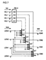
Die Umsetzung des logischen Speicheransteuersignals lsas in das physikalische Speicheransteuersignal sas ist in Figur 7 dargestellt. Hierzu werden die vier Vorhandenseinleitungen VL0..3 - siehe Figur 3 - an eine dritte Dekodiereinheit DK-3 geführt. Die vier Ausgänge A1..A4 der dritten Dekodiereinheit DK-3 sind jeweils mit einem Steuereingang ST von vier Schiebestufen S1..4 verbunden.The conversion of the logic memory drive signal lsas into the physical memory drive signal sas is shown in FIG. For this purpose, the four introductions VL0..3 - see FIG. 3 - are routed to a third decoding unit DK-3. The four outputs A1..A4 of the third decoding unit DK-3 are each connected to a control input ST of four shift stages S1..4.
Die Ausgänge LEN0..3 der vier UND-Gatter &(1..4) - siehe Figur 6 - sind wie folgt auf die vier Schiebestufen S1..4 geschaltet:
- Ausgang LEN0 auf einen Eingang der vierten Schiebestufe S4,
- Ausgang LEN1 auf einen Eingang der vierten und dritten Schiebestufe S3, S4,
- der Ausgang LEN2 auf einen Eingang der zweiten, dritten und vierten Schiebestufe S2..4 und
- LEN3 auf jeweils einen Eingang aller vier Schiebestufen S1..4.
- Output LEN0 to an input of the fourth shift stage S4,
- Output LEN1 to an input of the fourth and third shift stages S3, S4,
- the output LEN2 to an input of the second, third and fourth shift stage S2..4 and
- LEN3 to one input of all four sliding levels S1..4.
Die Schiebestufen S1..4 sind in gleicher Weise wie in Figur 3 oder 5 dargestellt, realisiert. In der dritten Dekodiereinheit DK-3 ist eine nicht dargestellte Dekodiertabelle hinterlegt, durch die die Schiebestufen S1..4 derart angesteuert werden, daß an den vier Ausgängen EN0..3 der vier Schiebestufen S1..4 das Speicheransteuersignal sas in binärer Form vorliegt, wobei jeweils ein Ausgang EN0..3 separat mit einem Einsetzbereich EB1..4 verbunden ist. Dies bedeutet, daß eine der vier Ausgänge EN0..3 eine binäre 1-Information aufweist, durch die das in den betreffenden Einsetzbereich EB1..4 eingesetzte Speichermodul SM angesteuert, das heißt, freigegeben wird. Zusammen mit den Adreßinformationen AD2-m der übrigen Adreßleitungen ADL2-m, wird der Subspeicherbereich in dem freigegebenen Speichermodul SM angesteuert und vom Mikroprozessor MP übermittelte Daten gespeichert oder Daten gelesen und an den Mikroprozessor MP übermittelt. Bezogen auf das Ausführungsbeispiel wird das im dritten Einsetzbereich EB3 eingesetzte Speichermodul SM freigegeben, das heißt, adressiert.The sliding stages S1..4 are implemented in the same way as shown in FIG. 3 or 5. In the third decoding unit DK-3, a decoding table, not shown, is stored, by means of which the shift stages S1..4 are controlled in this way be that the memory control signal sas is present in binary form at the four outputs EN0..3 of the four shift stages S1..4, each output EN0..3 being separately connected to an insertion range EB1..4. This means that one of the four outputs EN0..3 has a binary 1 information, by means of which the memory module SM used in the relevant application area EB1..4 is controlled, that is, released. Together with the address information AD2-m of the other address lines ADL2-m, the sub-memory area in the released memory module SM is controlled and data transmitted by the microprocessor MP is stored or data is read and transmitted to the microprocessor MP. Based on the exemplary embodiment, the memory module SM used in the third application area EB3 is released, that is, addressed.
Claims (12)
daß aus den logischen Kapazitäts- und Konfigurationsinformationen (lki,lkoi) für jede mögliche Speicherkapazität (K1,4) eine jeweils deren logische Gesamtspeicherkapazität anzeigende, logische speicherkapazitätsindividuelle Kapazitätsinformationen (klki) gebildet werden.A method according to claim 8, characterized in
that from the logical capacity and configuration information (lki, lkoi) for each possible storage capacity (K1,4) a logical storage capacity-specific capacity information (klki) is displayed, each showing its total logical storage capacity.
daß aus den aktuell vorliegenden Adreßinformationen der m-stelligen Speicherbereichsadresse (AD0..m) für jede vorgesehene Speicherkapazität (K1,4) abgeleiteten logischen Speicheransteuersignale (lsas1,4) auf die logischen Konfigurationsinformationen (lkoi) abgebildet werden, wodurch ein logisches Speicheransteuersignal (lsas) gebildet wird.A method according to claim 8 or 9, characterized in
that from the currently available address information of the m-digit memory area address (AD0..m) for each intended memory capacity (K1,4) derived logical memory control signals (lsas1,4) are mapped onto the logical configuration information (lkoi), whereby a logical memory control signal (lsas ) is formed.
daß die Kofigurationsinformationen (koi) dekodiert das logische Speicheransteuersignal (lsas) auf den betroffenen Einsetzbereich (EB1..4) steuern, wobei das gesteuerte logische Speicheransteuersignal (lsas) das physikalische Speicheransteuersignal (sas) repräsentiert.Method according to one of claims 8 to 10, characterized in that
that the configuration information (koi) decodes the logic memory drive signal (lsas) to the affected application area (EB1..4), the controlled logic Memory drive signal (lsas) represents the physical memory drive signal (sas).
Applications Claiming Priority (2)
| Application Number | Priority Date | Filing Date | Title |
|---|---|---|---|
| DE19549061 | 1995-12-29 | ||
| DE19549061 | 1995-12-29 |
Publications (2)
| Publication Number | Publication Date |
|---|---|
| EP0782077A1 true EP0782077A1 (en) | 1997-07-02 |
| EP0782077B1 EP0782077B1 (en) | 2003-08-20 |
Family
ID=7781601
Family Applications (1)
| Application Number | Title | Priority Date | Filing Date |
|---|---|---|---|
| EP96119487A Expired - Lifetime EP0782077B1 (en) | 1995-12-29 | 1996-12-04 | Method and arrangement for converting memory addresses into memory control signals |
Country Status (5)
| Country | Link |
|---|---|
| US (1) | US6003110A (en) |
| EP (1) | EP0782077B1 (en) |
| JP (1) | JP3266529B2 (en) |
| DE (1) | DE59610672D1 (en) |
| SG (1) | SG46760A1 (en) |
Cited By (1)
| Publication number | Priority date | Publication date | Assignee | Title |
|---|---|---|---|---|
| GB2357602A (en) * | 1999-12-22 | 2001-06-27 | Nokia Mobile Phones Ltd | Memory controller for a memory array comprising different memory types |
Families Citing this family (5)
| Publication number | Priority date | Publication date | Assignee | Title |
|---|---|---|---|---|
| JPH09293015A (en) * | 1996-04-24 | 1997-11-11 | Mitsubishi Electric Corp | Memory system and semiconductor storage device used therein |
| JP3365283B2 (en) * | 1997-11-14 | 2003-01-08 | 日本電気株式会社 | Semiconductor storage device |
| JP3498021B2 (en) | 1999-10-07 | 2004-02-16 | エヌイーシーコンピュータテクノ株式会社 | Memory control method |
| US7339837B2 (en) * | 2004-05-18 | 2008-03-04 | Infineon Technologies Ag | Configurable embedded processor |
| US7308527B2 (en) * | 2005-01-24 | 2007-12-11 | International Business Machines Corporation | System for indicating a plug position for a memory module in a memory system |
Citations (2)
| Publication number | Priority date | Publication date | Assignee | Title |
|---|---|---|---|---|
| EP0285986A2 (en) * | 1987-04-01 | 1988-10-12 | International Business Machines Corporation | Data processing system with means for contiguously addressing memory |
| EP0289899A2 (en) * | 1987-05-04 | 1988-11-09 | Prime Computer, Inc. | Memory control system |
Family Cites Families (5)
| Publication number | Priority date | Publication date | Assignee | Title |
|---|---|---|---|---|
| US5119486A (en) * | 1989-01-17 | 1992-06-02 | Prime Computer | Memory board selection method and apparatus |
| JPH0715665B2 (en) * | 1991-06-10 | 1995-02-22 | インターナショナル・ビジネス・マシーンズ・コーポレイション | Personal computer |
| DE59206051D1 (en) * | 1992-02-28 | 1996-05-23 | Siemens Ag | Process for hierarchically administrable, identification-oriented release control for operator task-related access instructions to a database of a program-controlled communication system |
| US5446860A (en) * | 1993-01-11 | 1995-08-29 | Hewlett-Packard Company | Apparatus for determining a computer memory configuration of memory modules using presence detect bits shifted serially into a configuration register |
| EP0629952B1 (en) * | 1993-06-16 | 1999-09-01 | Bull HN Information Systems Italia S.p.A. | Variable interleaving level memory and related configuration unit |
-
1996
- 1996-12-04 EP EP96119487A patent/EP0782077B1/en not_active Expired - Lifetime
- 1996-12-04 DE DE59610672T patent/DE59610672D1/en not_active Expired - Lifetime
- 1996-12-10 SG SG1996011616A patent/SG46760A1/en unknown
- 1996-12-25 JP JP34590196A patent/JP3266529B2/en not_active Expired - Fee Related
- 1996-12-30 US US08/774,459 patent/US6003110A/en not_active Expired - Lifetime
Patent Citations (2)
| Publication number | Priority date | Publication date | Assignee | Title |
|---|---|---|---|---|
| EP0285986A2 (en) * | 1987-04-01 | 1988-10-12 | International Business Machines Corporation | Data processing system with means for contiguously addressing memory |
| EP0289899A2 (en) * | 1987-05-04 | 1988-11-09 | Prime Computer, Inc. | Memory control system |
Non-Patent Citations (1)
| Title |
|---|
| "DYNAMIC SELF-CONFIGURATION FOR MEMEORY CARDS ARRANGEMENT", IBM TECHNICAL DISCLOSURE BULLETIN, vol. 31, no. 12, 1 May 1989 (1989-05-01), pages 213 - 216, XP000110911 * |
Cited By (2)
| Publication number | Priority date | Publication date | Assignee | Title |
|---|---|---|---|---|
| GB2357602A (en) * | 1999-12-22 | 2001-06-27 | Nokia Mobile Phones Ltd | Memory controller for a memory array comprising different memory types |
| US6563739B2 (en) | 1999-12-22 | 2003-05-13 | Nokia Mobile Phones Limited | System and method for transferring data between different types of memory using a common data bus |
Also Published As
| Publication number | Publication date |
|---|---|
| JP3266529B2 (en) | 2002-03-18 |
| SG46760A1 (en) | 1998-02-20 |
| US6003110A (en) | 1999-12-14 |
| EP0782077B1 (en) | 2003-08-20 |
| DE59610672D1 (en) | 2003-09-25 |
| JPH09212413A (en) | 1997-08-15 |
Similar Documents
| Publication | Publication Date | Title |
|---|---|---|
| DE2803989C2 (en) | Digital data storage with random access | |
| DE3318829C2 (en) | Output stage of an interface in a bus system | |
| DE3015875A1 (en) | MEMORY ACCESS SYSTEM AND METHOD FOR ACCESSING A DIGITAL MEMORY SYSTEM | |
| DE3618136C2 (en) | ||
| DE3043100C2 (en) | ||
| DE2926322C2 (en) | Storage subsystem | |
| DE2364254B2 (en) | CIRCUIT ARRANGEMENT FOR DATA PROCESSING DEVICES | |
| DE2527062C3 (en) | Adaptable address decoder | |
| DE2364253A1 (en) | CIRCUIT ARRANGEMENT FOR MICROPROGRAMMED DATA PROCESSING DEVICES | |
| DE2213953C3 (en) | Circuit arrangement for displaying characters on the screen of a display device | |
| EP0782077A1 (en) | Method and arrangement for converting memory addresses into memory control signals | |
| DE3526521C2 (en) | ||
| DE3024153A1 (en) | STORAGE SUBSYSTEM | |
| DE1234054B (en) | Byte converter | |
| DE10036643A1 (en) | Method and device for controlling operating routines in motor vehicle engine control uses a processor module to link to a bus system like a select port interface bus via a bus input/output interface while communicating through it. | |
| DE2233164A1 (en) | CIRCUIT ARRANGEMENT FOR HIDING ANY SELECTABLE AREA OF A BIT SEQUENCE WHEN TRANSFERRED BETWEEN TWO REGISTERS | |
| EP0494329B1 (en) | Circuit device to map the logical address space of a processing unit onto the physical address space of a memory | |
| DE3105503A1 (en) | ASSOCIATIVE ACCESS MEMORY | |
| EP0880092B1 (en) | Program controlled device whose operating system is capable of being upgraded and the new version switched over to, without having to restart the device | |
| DE3149905A1 (en) | ELECTRONIC DEVICE | |
| DE2017879B2 (en) | Free access memory array | |
| DE3331043C2 (en) | ||
| EP0361143A2 (en) | Circuitry for the on-chip interleaved access to dynamic RAM modules | |
| DE10208073A1 (en) | Driver circuit for an LCD display | |
| EP0480331A2 (en) | Data processing system with display terminals |
Legal Events
| Date | Code | Title | Description |
|---|---|---|---|
| PUAI | Public reference made under article 153(3) epc to a published international application that has entered the european phase |
Free format text: ORIGINAL CODE: 0009012 |
|
| AK | Designated contracting states |
Kind code of ref document: A1 Designated state(s): DE FR GB IT NL |
|
| 17P | Request for examination filed |
Effective date: 19970721 |
|
| 17Q | First examination report despatched |
Effective date: 20010730 |
|
| GRAH | Despatch of communication of intention to grant a patent |
Free format text: ORIGINAL CODE: EPIDOS IGRA |
|
| GRAS | Grant fee paid |
Free format text: ORIGINAL CODE: EPIDOSNIGR3 |
|
| GRAA | (expected) grant |
Free format text: ORIGINAL CODE: 0009210 |
|
| AK | Designated contracting states |
Designated state(s): DE FR GB IT NL |
|
| PG25 | Lapsed in a contracting state [announced via postgrant information from national office to epo] |
Ref country code: NL Free format text: LAPSE BECAUSE OF FAILURE TO SUBMIT A TRANSLATION OF THE DESCRIPTION OR TO PAY THE FEE WITHIN THE PRESCRIBED TIME-LIMIT Effective date: 20030820 |
|
| REG | Reference to a national code |
Ref country code: GB Ref legal event code: FG4D Free format text: NOT ENGLISH |
|
| REF | Corresponds to: |
Ref document number: 59610672 Country of ref document: DE Date of ref document: 20030925 Kind code of ref document: P |
|
| GBT | Gb: translation of ep patent filed (gb section 77(6)(a)/1977) | ||
| NLV1 | Nl: lapsed or annulled due to failure to fulfill the requirements of art. 29p and 29m of the patents act | ||
| ET | Fr: translation filed | ||
| PLBE | No opposition filed within time limit |
Free format text: ORIGINAL CODE: 0009261 |
|
| STAA | Information on the status of an ep patent application or granted ep patent |
Free format text: STATUS: NO OPPOSITION FILED WITHIN TIME LIMIT |
|
| REG | Reference to a national code |
Ref country code: HK Ref legal event code: WD Ref document number: 1000843 Country of ref document: HK |
|
| 26N | No opposition filed |
Effective date: 20040524 |
|
| REG | Reference to a national code |
Ref country code: GB Ref legal event code: 732E Free format text: REGISTERED BETWEEN 20121025 AND 20121031 |
|
| REG | Reference to a national code |
Ref country code: FR Ref legal event code: TP Owner name: SIEMENS ENTERPRISE COMMUNICATIONS GMBH & CO. K, DE Effective date: 20130108 |
|
| REG | Reference to a national code |
Ref country code: DE Ref legal event code: R082 Ref document number: 59610672 Country of ref document: DE Representative=s name: FRITZSCHE PATENT, DE |
|
| REG | Reference to a national code |
Ref country code: DE Ref legal event code: R082 Ref document number: 59610672 Country of ref document: DE Representative=s name: FRITZSCHE PATENTANWAELTE, DE Effective date: 20130313 Ref country code: DE Ref legal event code: R082 Ref document number: 59610672 Country of ref document: DE Representative=s name: FRITZSCHE PATENT, DE Effective date: 20130313 Ref country code: DE Ref legal event code: R081 Ref document number: 59610672 Country of ref document: DE Owner name: UNIFY GMBH & CO. KG, DE Free format text: FORMER OWNER: SIEMENS AKTIENGESELLSCHAFT, 80333 MUENCHEN, DE Effective date: 20130313 Ref country code: DE Ref legal event code: R081 Ref document number: 59610672 Country of ref document: DE Owner name: SIEMENS ENTERPRISE COMMUNICATIONS GMBH & CO. K, DE Free format text: FORMER OWNER: SIEMENS AKTIENGESELLSCHAFT, 80333 MUENCHEN, DE Effective date: 20130313 |
|
| REG | Reference to a national code |
Ref country code: DE Ref legal event code: R082 Ref document number: 59610672 Country of ref document: DE Representative=s name: FRITZSCHE PATENT, DE |
|
| REG | Reference to a national code |
Ref country code: DE Ref legal event code: R082 Ref document number: 59610672 Country of ref document: DE Representative=s name: FRITZSCHE PATENTANWAELTE, DE Effective date: 20131112 Ref country code: DE Ref legal event code: R082 Ref document number: 59610672 Country of ref document: DE Representative=s name: FRITZSCHE PATENT, DE Effective date: 20131112 Ref country code: DE Ref legal event code: R081 Ref document number: 59610672 Country of ref document: DE Owner name: UNIFY GMBH & CO. KG, DE Free format text: FORMER OWNER: SIEMENS ENTERPRISE COMMUNICATIONS GMBH & CO. KG, 81379 MUENCHEN, DE Effective date: 20131112 |
|
| REG | Reference to a national code |
Ref country code: FR Ref legal event code: CD Owner name: UNIFY GMBH & CO.KG, DE Effective date: 20140429 |
|
| PGFP | Annual fee paid to national office [announced via postgrant information from national office to epo] |
Ref country code: GB Payment date: 20141216 Year of fee payment: 19 |
|
| PGFP | Annual fee paid to national office [announced via postgrant information from national office to epo] |
Ref country code: FR Payment date: 20141212 Year of fee payment: 19 |
|
| PGFP | Annual fee paid to national office [announced via postgrant information from national office to epo] |
Ref country code: IT Payment date: 20141218 Year of fee payment: 19 |
|
| PGFP | Annual fee paid to national office [announced via postgrant information from national office to epo] |
Ref country code: DE Payment date: 20151217 Year of fee payment: 20 |
|
| GBPC | Gb: european patent ceased through non-payment of renewal fee |
Effective date: 20151204 |
|
| REG | Reference to a national code |
Ref country code: DE Ref legal event code: R082 Ref document number: 59610672 Country of ref document: DE Representative=s name: FRITZSCHE PATENTANWAELTE, DE Ref country code: DE Ref legal event code: R081 Ref document number: 59610672 Country of ref document: DE Owner name: UNIFY GMBH & CO. KG, DE Free format text: FORMER OWNER: UNIFY GMBH & CO. KG, 81379 MUENCHEN, DE |
|
| REG | Reference to a national code |
Ref country code: FR Ref legal event code: ST Effective date: 20160831 |
|
| PG25 | Lapsed in a contracting state [announced via postgrant information from national office to epo] |
Ref country code: GB Free format text: LAPSE BECAUSE OF NON-PAYMENT OF DUE FEES Effective date: 20151204 |
|
| PG25 | Lapsed in a contracting state [announced via postgrant information from national office to epo] |
Ref country code: FR Free format text: LAPSE BECAUSE OF NON-PAYMENT OF DUE FEES Effective date: 20151231 |
|
| REG | Reference to a national code |
Ref country code: DE Ref legal event code: R071 Ref document number: 59610672 Country of ref document: DE |
|
| PG25 | Lapsed in a contracting state [announced via postgrant information from national office to epo] |
Ref country code: IT Free format text: LAPSE BECAUSE OF NON-PAYMENT OF DUE FEES Effective date: 20151204 |