EP0788166A2 - Integrated circuit chip having gate array book personalisation using local interconnect - Google Patents
Integrated circuit chip having gate array book personalisation using local interconnect Download PDFInfo
- Publication number
- EP0788166A2 EP0788166A2 EP96309584A EP96309584A EP0788166A2 EP 0788166 A2 EP0788166 A2 EP 0788166A2 EP 96309584 A EP96309584 A EP 96309584A EP 96309584 A EP96309584 A EP 96309584A EP 0788166 A2 EP0788166 A2 EP 0788166A2
- Authority
- EP
- European Patent Office
- Prior art keywords
- local interconnect
- gate array
- integrated circuit
- circuit chip
- gate
- Prior art date
- Legal status (The legal status is an assumption and is not a legal conclusion. Google has not performed a legal analysis and makes no representation as to the accuracy of the status listed.)
- Withdrawn
Links
Images

Classifications
-
- H—ELECTRICITY
- H01—ELECTRIC ELEMENTS
- H01L—SEMICONDUCTOR DEVICES NOT COVERED BY CLASS H10
- H01L27/00—Devices consisting of a plurality of semiconductor or other solid-state components formed in or on a common substrate
- H01L27/02—Devices consisting of a plurality of semiconductor or other solid-state components formed in or on a common substrate including semiconductor components specially adapted for rectifying, oscillating, amplifying or switching and having at least one potential-jump barrier or surface barrier; including integrated passive circuit elements with at least one potential-jump barrier or surface barrier
- H01L27/04—Devices consisting of a plurality of semiconductor or other solid-state components formed in or on a common substrate including semiconductor components specially adapted for rectifying, oscillating, amplifying or switching and having at least one potential-jump barrier or surface barrier; including integrated passive circuit elements with at least one potential-jump barrier or surface barrier the substrate being a semiconductor body
- H01L27/10—Devices consisting of a plurality of semiconductor or other solid-state components formed in or on a common substrate including semiconductor components specially adapted for rectifying, oscillating, amplifying or switching and having at least one potential-jump barrier or surface barrier; including integrated passive circuit elements with at least one potential-jump barrier or surface barrier the substrate being a semiconductor body including a plurality of individual components in a repetitive configuration
- H01L27/118—Masterslice integrated circuits
- H01L27/11803—Masterslice integrated circuits using field effect technology
- H01L27/11807—CMOS gate arrays
-
- H—ELECTRICITY
- H01—ELECTRIC ELEMENTS
- H01L—SEMICONDUCTOR DEVICES NOT COVERED BY CLASS H10
- H01L21/00—Processes or apparatus adapted for the manufacture or treatment of semiconductor or solid state devices or of parts thereof
- H01L21/02—Manufacture or treatment of semiconductor devices or of parts thereof
- H01L21/04—Manufacture or treatment of semiconductor devices or of parts thereof the devices having at least one potential-jump barrier or surface barrier, e.g. PN junction, depletion layer or carrier concentration layer
- H01L21/18—Manufacture or treatment of semiconductor devices or of parts thereof the devices having at least one potential-jump barrier or surface barrier, e.g. PN junction, depletion layer or carrier concentration layer the devices having semiconductor bodies comprising elements of Group IV of the Periodic System or AIIIBV compounds with or without impurities, e.g. doping materials
- H01L21/28—Manufacture of electrodes on semiconductor bodies using processes or apparatus not provided for in groups H01L21/20 - H01L21/268
-
- H—ELECTRICITY
- H01—ELECTRIC ELEMENTS
- H01L—SEMICONDUCTOR DEVICES NOT COVERED BY CLASS H10
- H01L27/00—Devices consisting of a plurality of semiconductor or other solid-state components formed in or on a common substrate
- H01L27/02—Devices consisting of a plurality of semiconductor or other solid-state components formed in or on a common substrate including semiconductor components specially adapted for rectifying, oscillating, amplifying or switching and having at least one potential-jump barrier or surface barrier; including integrated passive circuit elements with at least one potential-jump barrier or surface barrier
- H01L27/0203—Particular design considerations for integrated circuits
- H01L27/0207—Geometrical layout of the components, e.g. computer aided design; custom LSI, semi-custom LSI, standard cell technique
Definitions
- the present invention relates to the use of a local interconnect layer in semiconductor devices. More particularly, this invention relates to the utilization of the local interconnect layer in gate array cells.
- a gate array cell on a complementary metal oxide semiconductor (CMOS) device typically comprises several transistors which will include an equal number of N-channel (NMOS) transistors and P-channel (PMOS) transistors.
- CMOS complementary metal oxide semiconductor
- One or more gate array cells are typically grouped together in "gate array books” to form logic devices such as NAND or OR gates.
- Each gate array book is "personalized” (i.e., customized to perform a specific logic function) by interconnecting conductors between the various contact points found within the gate array book.
- each gate array book includes the source, drain and gates of each transistor, antenna-protection diodes, supply voltage (e.g., VDD) and ground requirements, N-well and P-well contacts, biasing connections, tie-offs, and diffusion areas.
- VDD supply voltage
- N-well and P-well contacts biasing connections
- tie-offs and diffusion areas.
- Gate array cells are discussed in some detail in U.S. Pat. No. 4,412,237 by N. Matsumura et al., filed on Dec. 11, 1978 and issued on Oct. 25, 1983, which is herein incorporated by reference.
- the local interconnect layer is a type of interconnect conductor traditionally used for connecting closely spaced elements in a layout design.
- Local interconnect exists on a layer below the standard metal layers (e.g., metal-1) and therefore proximate to both transistor gates (i.e., the "polysilicon") and the diffused silicon region.
- Many advanced semiconductor technologies utilize the local interconnect layer for direct connections to diffusion or polysilicon in order to achieve considerable density improvement in custom and standard cell structures.
- U.S. Pat. No. 5,227,649 issued to Chapman on July 13, 1993, entitled “Circuit Layout And Method For VLSI Circuits Having Local Interconnects" discloses such a system in which local interconnect is utilized to bridge segments within an SRAM device.
- this local interconnect is not been within gate array books. Since gate array books may comprise a large percentage of a particular chip design, much of the benefit of the local interconnect layer may be lost without a gate array book layout that utilizes the interconnect layer.
- M-1 metal-1
- This method requires that a point-to-point connection must first run from a first contact point vertically up a contact opening to the M-1 layer, across the M-1 layer, and back down a contact opening to a second contact point.
- the local interconnect to connect certain contact points within gate array books (e.g., diffusion to diffusion)
- the need to go up to another layer is eliminated.
- the present invention seeks to minimize further the use of the M-1 level by utilizing the local interconnect layer as means for interconnecting gate array designs in a more efficient manner.
- the present invention provides a gate array book which includes at least one interconnection that utilizes the local interconnect layer to provide the necessary electrical connection by means of N-well and a P-well contact straps fabricated from said local interconnect conductor which run substantially the entire width of said gate array book across the top and bottom edges thereof.
- the placement of the contact strap at the top and bottom edges of the gate array allows for efficient fabrication in that it guarantees that a biasing conductor or tie-off fabricated from local interconnect will be available to any gate in the book.
- These additional interconnect conductors run in a primarily vertical direction, orthogonically to the straps.
- a local interconnect layer may be used for an N-well and P-well biasing conductor, unused PMOS or NMOS transistor tie-offs and displacement of PMOS or NMOS diffusion contacts. It may also be used for connecting PMOS and NMOS gates to antenna protection diodes, PMOS gates to an antenna-protection diode and then to an NMOS gate, PMOS diffusion to NMOS diffusion, PMOS diffusion to an NMOS gate, and an NMOS diffusion to a PMOS gate. It is recognized these embodiments are merely examples of the possible gate array cell interconnections available within the scope of this invention. It should also be recognized that this invention is not necessarily limited to CMOS technology.
- the present invention provides an integrated circuit chip which utilizes the local interconnect level for gate array cell connections and reduces usage of the metal-1 layer for gate array cell interconnections.
- FIG. 1 depicts an unpersonalized gate array cell 10.
- the cell 10 includes two P-channel (PMOS) transistors 16 and 18 and two N-channel (NMOS) transistors 32 and 34.
- the P-channel transistors include polysilicon gate electrodes (polygates) 22 and a P-type source/drain diffusion region 12.
- the N-channel transistors include polygates 26 and an N-type source/drain diffusion region 28.
- Other components on gate array cell 10 include N-well 11, N-well N+ diffusion 13, P+ implant 14, power (VDD) 20, ground (GND) 30, P+ implant 36, substrate P+ diffusion 38 and antenna-protection diodes 24. In general, those areas not within an N-well are a P-well and those diffusions which do not receive a P+ implant receive an N+ implant.
- gate array cell 10 is not capable of performing any logic functions. In order to do so, the cell needs to be personalized (i.e., electrical interconnections between contact points within the cell and possibly electrical connections with other cells must be made). As previously mentioned, the traditional method for making such interconnections has been to utilize the metal-1 layer which limits the overall availability of the metal-1 layer. FIGS. 2 and 3 depict examples of how such interconnections can be made pursuant to the present invention using the local interconnect layer.
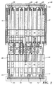
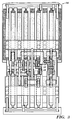
- FIG. 2 a gate array book is depicted personalized to form a 3-way AND logic gate 40 while FIG. 3 shows an XOR logic gate 54. As shown, various connections are depicted which utilize the local interconnect layer and therefore reduce the need to use the metal-1 layer. As depicted in FIG. 2, the left and right edges of book 40 end in P-channel (PMOS) 41 and N-channel (NMOS) 43 diffusions connected to VDD 45 and GND 47 respectively, which are shared with books placed horizontally adjacent (not shown).
- PMOS P-channel
- NMOS N-channel
- a first category of locations where local interconnect can be used involves the area at the top and bottom of the gate array book 40.
- Local interconnect may be used for N-well and P-well contact straps 42 which connect adjacent N-well and P-well contact at the upper and lower edges of the cell 40.
- Contact straps 42 are also shared with gate array or standard cell books placed above or below a given book.
- Local interconnect may also be utilized with the local biasing interconnect 44 which connects diffusions to the N-well and P-well contact straps 42 in order to bias them to VDD and GND, respectively.
- a third location local interconnect may be used is for tie-offs 46 which comprise short segments of local interconnect to turn off any devices required for gate isolation.
- the second general category of connections where the local interconnect is utilized pursuant to this invention is in the area between the PMOS diffusion and the NMOS diffusion. This typically is the area where the logic input and output lines attach to the gate array book and many of the necessary interconnections are made.
- each gate array cell layout provides one antenna-protection diode between the inboard gate connections of each pair of PMOS and NMOS devices. This ratio allows any single device or vertically adjacent pair of devices to be defined as a book input with the addition of a short segment of local interconnect 52. (Many schemes cannot support a ratio this high and thus require book inputs to be spread out, potentially wasting devices and reducing density).
- FIGS. 1 Pursuant to the layouts shown in FIGS.
- the gate array cells provide a personalization scheme where local interconnect primarily runs in one direction (vertically) and metal-1 connections run in an orthogonal direction (horizontally).
- the horizontal metal-1 wiring maximizes the metal-2 accessibility of pins and allows many pins to be accessed by metal-1 from the right and left edges of a book.
- local interconnect may be used for gate-to-gate connections 52 that may connect a PMOS gate to an antenna-protection diode and further connect to an NMOS gate. Additionally, local interconnect may be used for PMOS to NMOS connections 48 between PMOS and NMOS source or drain diffusions. This type of connection spans the entire area between the two diffusion regions. Similarly, local interconnect may be used to displace a diffusion contact 50 into the area between the devices. The displacement 50 provides at least three vertically adjacent locations where connections to an orthogonal metal-1 wire may be made. In more complex designs, the PMOS and NMOS diffusion connections can each be displaced one track toward the other without being connected, thus providing a pair of cross-unders.
- a gate array book personalized to form an XOR logic gate 54 is shown depicting further possible uses for local interconnect within a gate array book.
- local interconnect 58 is used to connect a PMOS gate to an antenna protection diode.
- NMOS gate connected to an antenna protection diode
- the local interconnect run horizontally in this area.
- short jogs of local interconnect 56 allow connections between PMOS source or drain diffusions and NMOS gates. Similar jogs may be used to connect NMOS source or drain diffusions and PMOS gates.
- the local interconnect may be fabricated from robust damascene tungsten, such as that disclosed by F. While et al, in "Damascene Stud Local Interconnect in CMOS Technology," 1992 IEEE International Electron Devices Meeting Digest of Technical Papers, p.301, which is hereby incorporated by reference.
Abstract
A gate array book layout for an integrated circuit chip is disclosed in which a local interconnect layer provides N-well and P-well contact straps extending substantially along the entire width of said gate array book across the top and bottom edges thereof. This enables efficient electrical connections between the various connection points located within the book. In particular, primarily vertical strips of local interconnect are used to connect contact points which exist at or near the same layer as the local interconnect layer. By using local interconnect in this manner, metal-1 layer usage is significantly reduced thereby allowing for a more efficient integrated circuit chip design.
Description
- The present invention relates to the use of a local interconnect layer in semiconductor devices. More particularly, this invention relates to the utilization of the local interconnect layer in gate array cells.
- One of the fundamental technologies available for allowing integrated circuit chip designers to place large numbers of logic circuits on a single or common very large scale integrated (VLSI) chip involves the use of gate array cells. Under this technology, rows of transistors are arranged in cells on the surface of the chip. A gate array cell on a complementary metal oxide semiconductor (CMOS) device typically comprises several transistors which will include an equal number of N-channel (NMOS) transistors and P-channel (PMOS) transistors. One or more gate array cells are typically grouped together in "gate array books" to form logic devices such as NAND or OR gates. Each gate array book is "personalized" (i.e., customized to perform a specific logic function) by interconnecting conductors between the various contact points found within the gate array book.
- Contact points found within each gate array book include the source, drain and gates of each transistor, antenna-protection diodes, supply voltage (e.g., VDD) and ground requirements, N-well and P-well contacts, biasing connections, tie-offs, and diffusion areas. Gate array cells are discussed in some detail in U.S. Pat. No. 4,412,237 by N. Matsumura et al., filed on Dec. 11, 1978 and issued on Oct. 25, 1983, which is herein incorporated by reference.
- An ongoing challenge faced by integrated circuit device manufacturers, including those which use gate array cells, is the desire to achieve more efficient circuit designs and provide for higher circuit densities. Because each individual gate array book will require many electrical interconnections between the various contact points of the gate array cells, interconnections inherently cause design limitations. This invention seeks to utilize the local interconnect layer as a means for interconnecting contact points in gate array books to achieve a more efficient design and high circuit density.
- The local interconnect layer is a type of interconnect conductor traditionally used for connecting closely spaced elements in a layout design. Local interconnect exists on a layer below the standard metal layers (e.g., metal-1) and therefore proximate to both transistor gates (i.e., the "polysilicon") and the diffused silicon region. Many advanced semiconductor technologies utilize the local interconnect layer for direct connections to diffusion or polysilicon in order to achieve considerable density improvement in custom and standard cell structures. For example, U.S. Pat. No. 5,227,649 issued to Chapman on July 13, 1993, entitled "Circuit Layout And Method For VLSI Circuits Having Local Interconnects" discloses such a system in which local interconnect is utilized to bridge segments within an SRAM device. However, this local interconnect is not been within gate array books. Since gate array books may comprise a large percentage of a particular chip design, much of the benefit of the local interconnect layer may be lost without a gate array book layout that utilizes the interconnect layer.
- The use of local interconnect conductors to personalize gate array books by connecting contact points to diffusion regions of transistors is shown in EP 0610771 A1.
- The use of local interconnect within gate array books provides a significant improvement since many of the contact points required to personalize and power the gate array cells are found near the local interconnect layer.
- The traditional means for interconnecting these various contact points has been to use the "metal-1" (M-1) layer. This method requires that a point-to-point connection must first run from a first contact point vertically up a contact opening to the M-1 layer, across the M-1 layer, and back down a contact opening to a second contact point. By using the local interconnect to connect certain contact points within gate array books (e.g., diffusion to diffusion), the need to go up to another layer is eliminated. The present invention seeks to minimize further the use of the M-1 level by utilizing the local interconnect layer as means for interconnecting gate array designs in a more efficient manner.
- The present invention provides a gate array book which includes at least one interconnection that utilizes the local interconnect layer to provide the necessary electrical connection by means of N-well and a P-well contact straps fabricated from said local interconnect conductor which run substantially the entire width of said gate array book across the top and bottom edges thereof. The placement of the contact strap at the top and bottom edges of the gate array allows for efficient fabrication in that it guarantees that a biasing conductor or tie-off fabricated from local interconnect will be available to any gate in the book. These additional interconnect conductors run in a primarily vertical direction, orthogonically to the straps.
- Several preferred embodiments are disclosed in which local interconnect technology has been used in gate array layouts. For example, in addition to the N-well and P-well straps, a local interconnect layer may be used for an N-well and P-well biasing conductor, unused PMOS or NMOS transistor tie-offs and displacement of PMOS or NMOS diffusion contacts. It may also be used for connecting PMOS and NMOS gates to antenna protection diodes, PMOS gates to an antenna-protection diode and then to an NMOS gate, PMOS diffusion to NMOS diffusion, PMOS diffusion to an NMOS gate, and an NMOS diffusion to a PMOS gate. It is recognized these embodiments are merely examples of the possible gate array cell interconnections available within the scope of this invention. It should also be recognized that this invention is not necessarily limited to CMOS technology.
- Thus, the present invention provides an integrated circuit chip which utilizes the local interconnect level for gate array cell connections and reduces usage of the metal-1 layer for gate array cell interconnections.
- It is a further advantage of the present invention to leave more metal-1 tracks available for global wiring and to provide a personalization scheme wherein local interconnect primarily runs one direction while metal-1 runs primarily in an orthogonal direction.
- The preferred exemplary embodiment of the present invention will hereinafter be described in conjunction with the appended drawings, where like designations denote like elements, and:
- FIG. 1 depicts an unpersonalized gate array cell;
- FIG. 2 depicts a gate array book forming part of an integrated circuit chip according to the invention and personalized using local interconnect to form a 3-way AND logic gate; and
- FIG. 3 depicts a gate array book forming part of an integrated circuit chip according to the invention and personalized using local interconnect to form an XOR logic gate.
- Referring now to the drawings, FIG. 1 depicts an unpersonalized
gate array cell 10. Thecell 10 includes two P-channel (PMOS)transistors transistors drain diffusion region 12. Similarly, the N-channel transistors includepolygates 26 and an N-type source/drain diffusion region 28. Other components ongate array cell 10 include N-well 11, N-well N+ diffusion 13,P+ implant 14, power (VDD) 20, ground (GND) 30,P+ implant 36,substrate P+ diffusion 38 and antenna-protection diodes 24. In general, those areas not within an N-well are a P-well and those diffusions which do not receive a P+ implant receive an N+ implant. - As shown,
gate array cell 10 is not capable of performing any logic functions. In order to do so, the cell needs to be personalized (i.e., electrical interconnections between contact points within the cell and possibly electrical connections with other cells must be made). As previously mentioned, the traditional method for making such interconnections has been to utilize the metal-1 layer which limits the overall availability of the metal-1 layer. FIGS. 2 and 3 depict examples of how such interconnections can be made pursuant to the present invention using the local interconnect layer. - In FIG. 2, a gate array book is depicted personalized to form a 3-way AND
logic gate 40 while FIG. 3 shows anXOR logic gate 54. As shown, various connections are depicted which utilize the local interconnect layer and therefore reduce the need to use the metal-1 layer. As depicted in FIG. 2, the left and right edges ofbook 40 end in P-channel (PMOS) 41 and N-channel (NMOS) 43 diffusions connected toVDD 45 andGND 47 respectively, which are shared with books placed horizontally adjacent (not shown). - Referring now to FIG. 2. a first category of locations where local interconnect can be used involves the area at the top and bottom of the
gate array book 40. Local interconnect may be used for N-well and P-well contact straps 42 which connect adjacent N-well and P-well contact at the upper and lower edges of thecell 40.Contact straps 42 are also shared with gate array or standard cell books placed above or below a given book. Local interconnect may also be utilized with thelocal biasing interconnect 44 which connects diffusions to the N-well and P-well contact straps 42 in order to bias them to VDD and GND, respectively. A third location local interconnect may be used is for tie-offs 46 which comprise short segments of local interconnect to turn off any devices required for gate isolation. This is accomplished by connecting the gates of any PMOS isolation devices to the N-well contact strap (VDD) and any NMOS isolation devices to the P-well contact strap (GND). Collectively, the above three usages for local interconnect provide a significant fraction of the connections required in a gate array book without the use or blockage of any metal-1. - The second general category of connections where the local interconnect is utilized pursuant to this invention is in the area between the PMOS diffusion and the NMOS diffusion. This typically is the area where the logic input and output lines attach to the gate array book and many of the necessary interconnections are made. Pursuant to the embodiments shown in FIGS. 2 and 3, each gate array cell layout provides one antenna-protection diode between the inboard gate connections of each pair of PMOS and NMOS devices. This ratio allows any single device or vertically adjacent pair of devices to be defined as a book input with the addition of a short segment of
local interconnect 52. (Many schemes cannot support a ratio this high and thus require book inputs to be spread out, potentially wasting devices and reducing density). Pursuant to the layouts shown in FIGS. 2 and 3, the gate array cells provide a personalization scheme where local interconnect primarily runs in one direction (vertically) and metal-1 connections run in an orthogonal direction (horizontally). The horizontal metal-1 wiring maximizes the metal-2 accessibility of pins and allows many pins to be accessed by metal-1 from the right and left edges of a book. - Referring now to FIG. 2, several examples of vertically running local interconnect are depicted within the area spanning the PMOS and NMOS diffusion regions. As shown, local interconnect may be used for gate-
to-gate connections 52 that may connect a PMOS gate to an antenna-protection diode and further connect to an NMOS gate. Additionally, local interconnect may be used for PMOS to NMOSconnections 48 between PMOS and NMOS source or drain diffusions. This type of connection spans the entire area between the two diffusion regions. Similarly, local interconnect may be used to displace adiffusion contact 50 into the area between the devices. Thedisplacement 50 provides at least three vertically adjacent locations where connections to an orthogonal metal-1 wire may be made. In more complex designs, the PMOS and NMOS diffusion connections can each be displaced one track toward the other without being connected, thus providing a pair of cross-unders. - Referring now to FIG. 3, a gate array book personalized to form an
XOR logic gate 54 is shown depicting further possible uses for local interconnect within a gate array book. Here,local interconnect 58 is used to connect a PMOS gate to an antenna protection diode. (Similarly, it would also be possible to have an NMOS gate connected to an antenna protection diode). Furthermore, it is possible, under certain circumstances to have the local interconnect run horizontally in this area. This is shown 59 as a PMOS gate connected to an antenna-protection diode, with a left-to-right jog, which is further connected to an NMOS gate. Furthermore, short jogs oflocal interconnect 56 allow connections between PMOS source or drain diffusions and NMOS gates. Similar jogs may be used to connect NMOS source or drain diffusions and PMOS gates. - While the exact materials and specifications for the implementation of this invention are not critical to its novelty, the local interconnect may be fabricated from robust damascene tungsten, such as that disclosed by F. While et al, in "Damascene Stud Local Interconnect in CMOS Technology," 1992 IEEE International Electron Devices Meeting Digest of Technical Papers, p.301, which is hereby incorporated by reference.
Claims (10)
- An integrated circuit chip comprising a plurality of gate array cells (10) arranged side by side to form a gate array book (40), said gate array book having a plurality of contact points and being personalized to perform a logic function by means of a local interconnect conductor (48, 50, 52), characterised in that :-said gate array book comprises an N-well and a P-well contact strap (42) fabricated from said local interconnect conductor and in that said N-well and P-well contact straps run substantially the entire width of said gate array book across the top and bottom edges thereof.
- An integrated circuit chip as claimed in claim 1 wherein said gate array book comprises:a plurality of P-channel transistors wherein each of said P-channel transistors includes a first plurality of contact points;a plurality of N-channel transistors wherein each of said N-channel transistors includes a second plurality of contact points;a third plurality of contact points located throughout said one gate array book; andsaid local interconnect conductor provides electrical connections between at least two said contact points.
- An integrated circuit chip as claimed in any preceding claim wherein said local interconnect conductor further comprises an N-well and a P-well biasing connection.
- An integrated circuit chip as claimed in any preceding claim wherein said local interconnect connectors further comprises at least one unused transistor tie-off.
- An integrated circuit chip as claimed in any preceding claim wherein said local interconnect conductor connects at least one transistor gate to an antenna-protection diode.
- An integrated circuit chip of as claimed in any preceding claim wherein said local interconnect conductor connects a PMOS gate to an antenna-protection diode to an NMOS gate.
- An integrated circuit chip as claimed in any preceding claim wherein said local interconnect conductor connects a PMOS diffusion to an NMOS diffusion.
- An integrated circuit chip as claimed in any preceding claim wherein said local interconnect conductor effect a displacement of at least one diffusion contact.
- An integrated circuit chip of as claimed in any preceding claim wherein said local interconnect conductor connects a PMOS diffusion to an NMOS gate.
- An integrated circuit chip of as claimed in any preceding claim wherein said local interconnect conductor connects an NMOS diffusion to a PMOS gate.
Applications Claiming Priority (2)
| Application Number | Priority Date | Filing Date | Title |
|---|---|---|---|
| US59505496A | 1996-01-31 | 1996-01-31 | |
| US595054 | 1996-01-31 |
Publications (2)
| Publication Number | Publication Date |
|---|---|
| EP0788166A2 true EP0788166A2 (en) | 1997-08-06 |
| EP0788166A3 EP0788166A3 (en) | 1999-11-24 |
Family
ID=24381526
Family Applications (1)
| Application Number | Title | Priority Date | Filing Date |
|---|---|---|---|
| EP96309584A Withdrawn EP0788166A3 (en) | 1996-01-31 | 1996-12-31 | Integrated circuit chip having gate array book personalisation using local interconnect |
Country Status (4)
| Country | Link |
|---|---|
| EP (1) | EP0788166A3 (en) |
| JP (1) | JPH09213915A (en) |
| KR (1) | KR100229577B1 (en) |
| IL (1) | IL119960A0 (en) |
Cited By (23)
| Publication number | Priority date | Publication date | Assignee | Title |
|---|---|---|---|---|
| US8541879B2 (en) | 2007-12-13 | 2013-09-24 | Tela Innovations, Inc. | Super-self-aligned contacts and method for making the same |
| US8549455B2 (en) | 2007-08-02 | 2013-10-01 | Tela Innovations, Inc. | Methods for cell phasing and placement in dynamic array architecture and implementation of the same |
| US8552508B2 (en) | 2008-03-13 | 2013-10-08 | Tela Innovations, Inc. | Integrated circuit including cross-coupled transistors having gate electrodes formed within gate level feature layout channels with shared diffusion regions on opposite sides of two-transistor-forming gate level feature and electrical connection of transistor gates through linear interconnect conductors in single interconnect layer |
| US8653857B2 (en) | 2006-03-09 | 2014-02-18 | Tela Innovations, Inc. | Circuitry and layouts for XOR and XNOR logic |
| US8661392B2 (en) | 2009-10-13 | 2014-02-25 | Tela Innovations, Inc. | Methods for cell boundary encroachment and layouts implementing the Same |
| US8658542B2 (en) | 2006-03-09 | 2014-02-25 | Tela Innovations, Inc. | Coarse grid design methods and structures |
| US8667443B2 (en) | 2007-03-05 | 2014-03-04 | Tela Innovations, Inc. | Integrated circuit cell library for multiple patterning |
| US8680626B2 (en) | 2007-10-26 | 2014-03-25 | Tela Innovations, Inc. | Methods, structures, and designs for self-aligning local interconnects used in integrated circuits |
| US8701071B2 (en) | 2008-01-31 | 2014-04-15 | Tela Innovations, Inc. | Enforcement of semiconductor structure regularity for localized transistors and interconnect |
| US8756551B2 (en) | 2007-08-02 | 2014-06-17 | Tela Innovations, Inc. | Methods for designing semiconductor device with dynamic array section |
| US8759985B2 (en) | 2008-03-27 | 2014-06-24 | Tela Innovations, Inc. | Methods for multi-wire routing and apparatus implementing same |
| US8823062B2 (en) | 2006-03-09 | 2014-09-02 | Tela Innovations, Inc. | Integrated circuit with offset line end spacings in linear gate electrode level |
| US8839175B2 (en) | 2006-03-09 | 2014-09-16 | Tela Innovations, Inc. | Scalable meta-data objects |
| US8863063B2 (en) | 2009-05-06 | 2014-10-14 | Tela Innovations, Inc. | Finfet transistor circuit |
| WO2014178949A1 (en) * | 2013-03-14 | 2014-11-06 | Qualcomm Incorporated | Local interconnect structures for high density |
| US9035359B2 (en) | 2006-03-09 | 2015-05-19 | Tela Innovations, Inc. | Semiconductor chip including region including linear-shaped conductive structures forming gate electrodes and having electrical connection areas arranged relative to inner region between transistors of different types and associated methods |
| US9122832B2 (en) | 2008-08-01 | 2015-09-01 | Tela Innovations, Inc. | Methods for controlling microloading variation in semiconductor wafer layout and fabrication |
| US9159627B2 (en) | 2010-11-12 | 2015-10-13 | Tela Innovations, Inc. | Methods for linewidth modification and apparatus implementing the same |
| US9230910B2 (en) | 2006-03-09 | 2016-01-05 | Tela Innovations, Inc. | Oversized contacts and vias in layout defined by linearly constrained topology |
| US9318476B2 (en) | 2014-03-03 | 2016-04-19 | Qualcomm Incorporated | High performance standard cell with continuous oxide definition and characterized leakage current |
| US9563733B2 (en) | 2009-05-06 | 2017-02-07 | Tela Innovations, Inc. | Cell circuit and layout with linear finfet structures |
| US9754878B2 (en) | 2006-03-09 | 2017-09-05 | Tela Innovations, Inc. | Semiconductor chip including a chip level based on a layout that includes both regular and irregular wires |
| US10692808B2 (en) | 2017-09-18 | 2020-06-23 | Qualcomm Incorporated | High performance cell design in a technology with high density metal routing |
Citations (3)
| Publication number | Priority date | Publication date | Assignee | Title |
|---|---|---|---|---|
| US4412237A (en) | 1977-12-30 | 1983-10-25 | Fujitsu Limited | Semiconductor device |
| US5227649A (en) | 1989-02-27 | 1993-07-13 | Texas Instruments Incorporated | Circuit layout and method for VLSI circuits having local interconnects |
| EP0610771A1 (en) | 1993-02-11 | 1994-08-17 | Siemens Aktiengesellschaft | Semiconductor arrangement with CMOS basic cells |
Family Cites Families (1)
| Publication number | Priority date | Publication date | Assignee | Title |
|---|---|---|---|---|
| JPS59232442A (en) * | 1983-06-16 | 1984-12-27 | Toshiba Corp | Semiconductor integrated circuit |
-
1996
- 1996-12-10 KR KR1019960063380A patent/KR100229577B1/en not_active IP Right Cessation
- 1996-12-31 EP EP96309584A patent/EP0788166A3/en not_active Withdrawn
-
1997
- 1997-01-02 IL IL11996097A patent/IL119960A0/en unknown
- 1997-01-21 JP JP9008569A patent/JPH09213915A/en active Pending
Patent Citations (3)
| Publication number | Priority date | Publication date | Assignee | Title |
|---|---|---|---|---|
| US4412237A (en) | 1977-12-30 | 1983-10-25 | Fujitsu Limited | Semiconductor device |
| US5227649A (en) | 1989-02-27 | 1993-07-13 | Texas Instruments Incorporated | Circuit layout and method for VLSI circuits having local interconnects |
| EP0610771A1 (en) | 1993-02-11 | 1994-08-17 | Siemens Aktiengesellschaft | Semiconductor arrangement with CMOS basic cells |
Non-Patent Citations (1)
| Title |
|---|
| "1992 IEEE International Electron Devices Meeting Digest of Technical Papers.", 1992, article WHILE F. ET AL.: "Damascene Stud Local Interconnect in CMOS Technology.", pages: 301 |
Cited By (110)
| Publication number | Priority date | Publication date | Assignee | Title |
|---|---|---|---|---|
| US9240413B2 (en) | 2006-03-09 | 2016-01-19 | Tela Innovations, Inc. | Methods, structures, and designs for self-aligning local interconnects used in integrated circuits |
| US8839175B2 (en) | 2006-03-09 | 2014-09-16 | Tela Innovations, Inc. | Scalable meta-data objects |
| US10217763B2 (en) | 2006-03-09 | 2019-02-26 | Tela Innovations, Inc. | Semiconductor chip having region including gate electrode features of rectangular shape on gate horizontal grid and first-metal structures of rectangular shape on at least eight first-metal gridlines of first-metal vertical grid |
| US8921896B2 (en) | 2006-03-09 | 2014-12-30 | Tela Innovations, Inc. | Integrated circuit including linear gate electrode structures having different extension distances beyond contact |
| US10141334B2 (en) | 2006-03-09 | 2018-11-27 | Tela Innovations, Inc. | Semiconductor chip including region having rectangular-shaped gate structures and first-metal structures |
| US10141335B2 (en) | 2006-03-09 | 2018-11-27 | Tela Innovations, Inc. | Semiconductor CIP including region having rectangular-shaped gate structures and first metal structures |
| US8946781B2 (en) | 2006-03-09 | 2015-02-03 | Tela Innovations, Inc. | Integrated circuit including gate electrode conductive structures with different extension distances beyond contact |
| US9917056B2 (en) | 2006-03-09 | 2018-03-13 | Tela Innovations, Inc. | Coarse grid design methods and structures |
| US8823062B2 (en) | 2006-03-09 | 2014-09-02 | Tela Innovations, Inc. | Integrated circuit with offset line end spacings in linear gate electrode level |
| US9905576B2 (en) | 2006-03-09 | 2018-02-27 | Tela Innovations, Inc. | Semiconductor chip including region having rectangular-shaped gate structures and first metal structures |
| US9859277B2 (en) | 2006-03-09 | 2018-01-02 | Tela Innovations, Inc. | Methods, structures, and designs for self-aligning local interconnects used in integrated circuits |
| US8653857B2 (en) | 2006-03-09 | 2014-02-18 | Tela Innovations, Inc. | Circuitry and layouts for XOR and XNOR logic |
| US9754878B2 (en) | 2006-03-09 | 2017-09-05 | Tela Innovations, Inc. | Semiconductor chip including a chip level based on a layout that includes both regular and irregular wires |
| US8658542B2 (en) | 2006-03-09 | 2014-02-25 | Tela Innovations, Inc. | Coarse grid design methods and structures |
| US8952425B2 (en) | 2006-03-09 | 2015-02-10 | Tela Innovations, Inc. | Integrated circuit including at least four linear-shaped conductive structures having extending portions of different length |
| US9741719B2 (en) | 2006-03-09 | 2017-08-22 | Tela Innovations, Inc. | Methods, structures, and designs for self-aligning local interconnects used in integrated circuits |
| US9711495B2 (en) | 2006-03-09 | 2017-07-18 | Tela Innovations, Inc. | Oversized contacts and vias in layout defined by linearly constrained topology |
| US9673825B2 (en) | 2006-03-09 | 2017-06-06 | Tela Innovations, Inc. | Circuitry and layouts for XOR and XNOR logic |
| US10186523B2 (en) | 2006-03-09 | 2019-01-22 | Tela Innovations, Inc. | Semiconductor chip having region including gate electrode features formed in part from rectangular layout shapes on gate horizontal grid and first-metal structures formed in part from rectangular layout shapes on at least eight first-metal gridlines of first-metal vertical grid |
| US10230377B2 (en) | 2006-03-09 | 2019-03-12 | Tela Innovations, Inc. | Circuitry and layouts for XOR and XNOR logic |
| US9443947B2 (en) | 2006-03-09 | 2016-09-13 | Tela Innovations, Inc. | Semiconductor chip including region having integrated circuit transistor gate electrodes formed by various conductive structures of specified shape and position and method for manufacturing the same |
| US9589091B2 (en) | 2006-03-09 | 2017-03-07 | Tela Innovations, Inc. | Scalable meta-data objects |
| US9425273B2 (en) | 2006-03-09 | 2016-08-23 | Tela Innovations, Inc. | Semiconductor chip including integrated circuit including at least five gate level conductive structures having particular spatial and electrical relationship and method for manufacturing the same |
| US9009641B2 (en) | 2006-03-09 | 2015-04-14 | Tela Innovations, Inc. | Circuits with linear finfet structures |
| US9425145B2 (en) | 2006-03-09 | 2016-08-23 | Tela Innovations, Inc. | Oversized contacts and vias in layout defined by linearly constrained topology |
| US9425272B2 (en) | 2006-03-09 | 2016-08-23 | Tela Innovations, Inc. | Semiconductor chip including integrated circuit including four transistors of first transistor type and four transistors of second transistor type with electrical connections between various transistors and methods for manufacturing the same |
| US9336344B2 (en) | 2006-03-09 | 2016-05-10 | Tela Innovations, Inc. | Coarse grid design methods and structures |
| US8921897B2 (en) | 2006-03-09 | 2014-12-30 | Tela Innovations, Inc. | Integrated circuit with gate electrode conductive structures having offset ends |
| US9230910B2 (en) | 2006-03-09 | 2016-01-05 | Tela Innovations, Inc. | Oversized contacts and vias in layout defined by linearly constrained topology |
| US9035359B2 (en) | 2006-03-09 | 2015-05-19 | Tela Innovations, Inc. | Semiconductor chip including region including linear-shaped conductive structures forming gate electrodes and having electrical connection areas arranged relative to inner region between transistors of different types and associated methods |
| US8667443B2 (en) | 2007-03-05 | 2014-03-04 | Tela Innovations, Inc. | Integrated circuit cell library for multiple patterning |
| US10074640B2 (en) | 2007-03-05 | 2018-09-11 | Tela Innovations, Inc. | Integrated circuit cell library for multiple patterning |
| US9633987B2 (en) | 2007-03-05 | 2017-04-25 | Tela Innovations, Inc. | Integrated circuit cell library for multiple patterning |
| US9424387B2 (en) | 2007-03-07 | 2016-08-23 | Tela Innovations, Inc. | Methods for cell phasing and placement in dynamic array architecture and implementation of the same |
| US8966424B2 (en) | 2007-03-07 | 2015-02-24 | Tela Innovations, Inc. | Methods for cell phasing and placement in dynamic array architecture and implementation of the same |
| US9910950B2 (en) | 2007-03-07 | 2018-03-06 | Tela Innovations, Inc. | Methods for cell phasing and placement in dynamic array architecture and implementation of the same |
| US9595515B2 (en) | 2007-03-07 | 2017-03-14 | Tela Innovations, Inc. | Semiconductor chip including integrated circuit defined within dynamic array section |
| US8759882B2 (en) | 2007-08-02 | 2014-06-24 | Tela Innovations, Inc. | Semiconductor device with dynamic array sections defined and placed according to manufacturing assurance halos |
| US8549455B2 (en) | 2007-08-02 | 2013-10-01 | Tela Innovations, Inc. | Methods for cell phasing and placement in dynamic array architecture and implementation of the same |
| US8756551B2 (en) | 2007-08-02 | 2014-06-17 | Tela Innovations, Inc. | Methods for designing semiconductor device with dynamic array section |
| US10734383B2 (en) | 2007-10-26 | 2020-08-04 | Tela Innovations, Inc. | Methods, structures, and designs for self-aligning local interconnects used in integrated circuits |
| US8680626B2 (en) | 2007-10-26 | 2014-03-25 | Tela Innovations, Inc. | Methods, structures, and designs for self-aligning local interconnects used in integrated circuits |
| US10461081B2 (en) | 2007-12-13 | 2019-10-29 | Tel Innovations, Inc. | Super-self-aligned contacts and method for making the same |
| US9818747B2 (en) | 2007-12-13 | 2017-11-14 | Tela Innovations, Inc. | Super-self-aligned contacts and method for making the same |
| US9281371B2 (en) | 2007-12-13 | 2016-03-08 | Tela Innovations, Inc. | Super-self-aligned contacts and method for making the same |
| US8541879B2 (en) | 2007-12-13 | 2013-09-24 | Tela Innovations, Inc. | Super-self-aligned contacts and method for making the same |
| US8951916B2 (en) | 2007-12-13 | 2015-02-10 | Tela Innovations, Inc. | Super-self-aligned contacts and method for making the same |
| US9202779B2 (en) | 2008-01-31 | 2015-12-01 | Tela Innovations, Inc. | Enforcement of semiconductor structure regularity for localized transistors and interconnect |
| US8701071B2 (en) | 2008-01-31 | 2014-04-15 | Tela Innovations, Inc. | Enforcement of semiconductor structure regularity for localized transistors and interconnect |
| US9530734B2 (en) | 2008-01-31 | 2016-12-27 | Tela Innovations, Inc. | Enforcement of semiconductor structure regularity for localized transistors and interconnect |
| US8587034B2 (en) | 2008-03-13 | 2013-11-19 | Tela Innovations, Inc. | Integrated circuit including cross-coupled transistors having gate electrodes formed within gate level feature layout channels with four inside positioned gate contacts and electrical connection of transistor gates through linear interconnect conductors in single interconnect layer |
| US8581303B2 (en) | 2008-03-13 | 2013-11-12 | Tela Innovations, Inc. | Integrated circuit including cross-coupled trasistors having gate electrodes formed within gate level feature layout channels with four inside positioned gate contacts having offset relationships and electrical connection of cross-coupled transistors through same interconnect layer |
| US8853794B2 (en) | 2008-03-13 | 2014-10-07 | Tela Innovations, Inc. | Integrated circuit within semiconductor chip including cross-coupled transistor configuration |
| US8772839B2 (en) | 2008-03-13 | 2014-07-08 | Tela Innovations, Inc. | Integrated circuit including cross-coupled transistors having gate electrodes formed within gate level feature layout channels with four inside positioned gate contacts having offset and aligned relationships and electrical connection of transistor gates through linear interconnect conductors in single interconnect layer |
| US9081931B2 (en) | 2008-03-13 | 2015-07-14 | Tela Innovations, Inc. | Cross-coupled transistor circuit having diffusion regions of common node on opposing sides of same gate electrode track and gate node connection through single interconnect layer |
| US9117050B2 (en) | 2008-03-13 | 2015-08-25 | Tela Innovations, Inc. | Integrated circuit including cross-coupled transistors having gate electrodes formed within gate level feature layout channels with gate contact position and offset specifications |
| US10727252B2 (en) | 2008-03-13 | 2020-07-28 | Tela Innovations, Inc. | Semiconductor chip including integrated circuit having cross-coupled transistor configuration and method for manufacturing the same |
| US10658385B2 (en) | 2008-03-13 | 2020-05-19 | Tela Innovations, Inc. | Cross-coupled transistor circuit defined on four gate electrode tracks |
| US10651200B2 (en) | 2008-03-13 | 2020-05-12 | Tela Innovations, Inc. | Cross-coupled transistor circuit defined on three gate electrode tracks |
| US8785979B2 (en) | 2008-03-13 | 2014-07-22 | Tela Innovations, Inc. | Integrated circuit including cross-coupled transistors having gate electrodes formed within gate level feature layout channels with two inside positioned gate contacts and two outside positioned gate contacts and electrical connection of cross-coupled transistors through same interconnect layer |
| US9208279B2 (en) | 2008-03-13 | 2015-12-08 | Tela Innovations, Inc. | Semiconductor chip including digital logic circuit including linear-shaped conductive structures having electrical connection areas located within inner region between transistors of different type and associated methods |
| US9213792B2 (en) | 2008-03-13 | 2015-12-15 | Tela Innovations, Inc. | Semiconductor chip including digital logic circuit including at least six transistors with some transistors forming cross-coupled transistor configuration and associated methods |
| US8853793B2 (en) | 2008-03-13 | 2014-10-07 | Tela Innovations, Inc. | Integrated circuit including gate electrode level region including cross-coupled transistors having gate contacts located over inner portion of gate electrode level region and offset gate level feature line ends |
| US8816402B2 (en) | 2008-03-13 | 2014-08-26 | Tela Innovations, Inc. | Integrated circuit including cross-coupled transistors having gate electrodes formed within gate level feature layout channels with gate level feature layout channel including single transistor |
| US9245081B2 (en) | 2008-03-13 | 2016-01-26 | Tela Innovations, Inc. | Semiconductor chip including digital logic circuit including at least nine linear-shaped conductive structures collectively forming gate electrodes of at least six transistors with some transistors forming cross-coupled transistor configuration and associated methods |
| US8552508B2 (en) | 2008-03-13 | 2013-10-08 | Tela Innovations, Inc. | Integrated circuit including cross-coupled transistors having gate electrodes formed within gate level feature layout channels with shared diffusion regions on opposite sides of two-transistor-forming gate level feature and electrical connection of transistor gates through linear interconnect conductors in single interconnect layer |
| US8835989B2 (en) | 2008-03-13 | 2014-09-16 | Tela Innovations, Inc. | Integrated circuit including cross-coupled transistors having gate electrodes formed within gate level feature layout channels with gate electrode placement specifications |
| US8558322B2 (en) | 2008-03-13 | 2013-10-15 | Tela Innovations, Inc. | Integrated circuit including cross-coupled transistors having gate electrodes formed within gate level feature layout channels with at least two gate electrodes electrically connected to each other through gate level feature |
| US8836045B2 (en) | 2008-03-13 | 2014-09-16 | Tela Innovations, Inc. | Cross-coupled transistor circuit having diffusion regions of common node on opposing sides of same gate electrode track |
| US8564071B2 (en) | 2008-03-13 | 2013-10-22 | Tela Innovations, Inc. | Integrated circuit including cross-coupled transistors having gate electrodes formed within gate level feature layout channels with at least two different gate level feature extensions beyond contact |
| US8742463B2 (en) | 2008-03-13 | 2014-06-03 | Tela Innovations, Inc. | Integrated circuit including cross-coupled transistors having gate electrodes formed within gate level feature layout channels with outer positioned gate contacts |
| US8742462B2 (en) | 2008-03-13 | 2014-06-03 | Tela Innovations, Inc. | Integrated circuit including cross-coupled transistors having gate electrodes formed within gate level feature layout channels with gate contact position specifications |
| US8735995B2 (en) | 2008-03-13 | 2014-05-27 | Tela Innovations, Inc. | Cross-coupled transistor circuit defined on three gate electrode tracks with diffusion regions of common node on opposing sides of same gate electrode track |
| US8735944B2 (en) | 2008-03-13 | 2014-05-27 | Tela Innovations, Inc. | Integrated circuit including cross-coupled transistors having gate electrodes formed within gate level feature layout channels with serially connected transistors |
| US8729643B2 (en) | 2008-03-13 | 2014-05-20 | Tela Innovations, Inc. | Cross-coupled transistor circuit including offset inner gate contacts |
| US8569841B2 (en) | 2008-03-13 | 2013-10-29 | Tela Innovations, Inc. | Integrated circuit including cross-coupled transistors having gate electrodes formed within gate level feature layout channels with at least one gate level feature extending into adjacent gate level feature layout channel |
| US8847331B2 (en) | 2008-03-13 | 2014-09-30 | Tela Innovations, Inc. | Semiconductor chip including region having cross-coupled transistor configuration with offset electrical connection areas on gate electrode forming conductive structures and at least two different inner extension distances of gate electrode forming conductive structures |
| US9536899B2 (en) | 2008-03-13 | 2017-01-03 | Tela Innovations, Inc. | Semiconductor chip including integrated circuit having cross-coupled transistor configuration and method for manufacturing the same |
| US8575706B2 (en) | 2008-03-13 | 2013-11-05 | Tela Innovations, Inc. | Integrated circuit including cross-coupled transistors having gate electrodes formed within gate level feature layout channels with at least two different gate level features inner extensions beyond gate electrode |
| US8729606B2 (en) | 2008-03-13 | 2014-05-20 | Tela Innovations, Inc. | Integrated circuit including cross-coupled transistors having gate electrodes formed within gate level feature layout channels |
| US10020321B2 (en) | 2008-03-13 | 2018-07-10 | Tela Innovations, Inc. | Cross-coupled transistor circuit defined on two gate electrode tracks |
| US8872283B2 (en) | 2008-03-13 | 2014-10-28 | Tela Innovations, Inc. | Integrated circuit including cross-coupled transistors having gate electrodes formed within gate level feature layout channels with shared diffusion regions on opposite sides of two-transistor-forming gate level feature |
| US8680583B2 (en) | 2008-03-13 | 2014-03-25 | Tela Innovations, Inc. | Integrated circuit including cross-coupled transistors having gate electrodes formed within at least nine gate level feature layout channels |
| US8581304B2 (en) | 2008-03-13 | 2013-11-12 | Tela Innovations, Inc. | Integrated circuit including cross-coupled transistors having gate electrodes formed within gate level feature layout channels with four inside positioned gate contacts having offset and aligned relationships |
| US8669594B2 (en) | 2008-03-13 | 2014-03-11 | Tela Innovations, Inc. | Integrated circuit including cross-coupled transistors having gate electrodes formed within at least twelve gate level feature layout channels |
| US8669595B2 (en) | 2008-03-13 | 2014-03-11 | Tela Innovations, Inc. | Integrated circuit including cross-coupled transistors having gate electrodes formed within gate level feature layout channels with gate contact position, alignment, and offset specifications |
| US8785978B2 (en) | 2008-03-13 | 2014-07-22 | Tela Innovations, Inc. | Integrated circuit including cross-coupled transistors having gate electrodes formed within gate level feature layout channels with electrical connection of cross-coupled transistors through same interconnect layer |
| US8847329B2 (en) | 2008-03-13 | 2014-09-30 | Tela Innovations, Inc. | Cross-coupled transistor circuit defined having diffusion regions of common node on opposing sides of same gate electrode track with at least two non-inner positioned gate contacts |
| US8866197B2 (en) | 2008-03-13 | 2014-10-21 | Tela Innovations, Inc. | Integrated circuit including cross-coupled transistors having gate electrodes formed within gate level feature layout channels with at least two gate electrodes electrically connected to each other through another transistor forming gate level feature |
| US9871056B2 (en) | 2008-03-13 | 2018-01-16 | Tela Innovations, Inc. | Semiconductor chip including integrated circuit having cross-coupled transistor configuration and method for manufacturing the same |
| US8592872B2 (en) | 2008-03-13 | 2013-11-26 | Tela Innovations, Inc. | Integrated circuit including cross-coupled transistors with two transistors of different type having gate electrodes formed by common gate level feature with shared diffusion regions on opposite sides of common gate level feature |
| US8759985B2 (en) | 2008-03-27 | 2014-06-24 | Tela Innovations, Inc. | Methods for multi-wire routing and apparatus implementing same |
| US9779200B2 (en) | 2008-03-27 | 2017-10-03 | Tela Innovations, Inc. | Methods for multi-wire routing and apparatus implementing same |
| US9390215B2 (en) | 2008-03-27 | 2016-07-12 | Tela Innovations, Inc. | Methods for multi-wire routing and apparatus implementing same |
| US9122832B2 (en) | 2008-08-01 | 2015-09-01 | Tela Innovations, Inc. | Methods for controlling microloading variation in semiconductor wafer layout and fabrication |
| US9563733B2 (en) | 2009-05-06 | 2017-02-07 | Tela Innovations, Inc. | Cell circuit and layout with linear finfet structures |
| US8863063B2 (en) | 2009-05-06 | 2014-10-14 | Tela Innovations, Inc. | Finfet transistor circuit |
| US10446536B2 (en) | 2009-05-06 | 2019-10-15 | Tela Innovations, Inc. | Cell circuit and layout with linear finfet structures |
| US8661392B2 (en) | 2009-10-13 | 2014-02-25 | Tela Innovations, Inc. | Methods for cell boundary encroachment and layouts implementing the Same |
| US9530795B2 (en) | 2009-10-13 | 2016-12-27 | Tela Innovations, Inc. | Methods for cell boundary encroachment and semiconductor devices implementing the same |
| US9269702B2 (en) | 2009-10-13 | 2016-02-23 | Tela Innovations, Inc. | Methods for cell boundary encroachment and layouts implementing the same |
| US9704845B2 (en) | 2010-11-12 | 2017-07-11 | Tela Innovations, Inc. | Methods for linewidth modification and apparatus implementing the same |
| US9159627B2 (en) | 2010-11-12 | 2015-10-13 | Tela Innovations, Inc. | Methods for linewidth modification and apparatus implementing the same |
| WO2014178949A1 (en) * | 2013-03-14 | 2014-11-06 | Qualcomm Incorporated | Local interconnect structures for high density |
| CN105009274A (en) * | 2013-03-14 | 2015-10-28 | 高通股份有限公司 | Local interconnect structures for high density |
| CN107424956A (en) * | 2013-03-14 | 2017-12-01 | 高通股份有限公司 | Circuit and its manufacture method with highdensity local interlinkage structure |
| US9024418B2 (en) | 2013-03-14 | 2015-05-05 | Qualcomm Incorporated | Local interconnect structures for high density |
| CN107424956B (en) * | 2013-03-14 | 2020-11-03 | 高通股份有限公司 | Circuit with high density local interconnect structure and method of making same |
| US9318476B2 (en) | 2014-03-03 | 2016-04-19 | Qualcomm Incorporated | High performance standard cell with continuous oxide definition and characterized leakage current |
| US10692808B2 (en) | 2017-09-18 | 2020-06-23 | Qualcomm Incorporated | High performance cell design in a technology with high density metal routing |
Also Published As
| Publication number | Publication date |
|---|---|
| IL119960A0 (en) | 1997-04-15 |
| EP0788166A3 (en) | 1999-11-24 |
| KR100229577B1 (en) | 1999-11-15 |
| JPH09213915A (en) | 1997-08-15 |
| KR970060389A (en) | 1997-08-12 |
Similar Documents
| Publication | Publication Date | Title |
|---|---|---|
| EP0788166A2 (en) | Integrated circuit chip having gate array book personalisation using local interconnect | |
| US7541647B2 (en) | Method of designing semiconductor integrated circuit device and semiconductor integrated circuit device | |
| EP0098163B1 (en) | Gate-array chip | |
| US6732344B2 (en) | Semiconductor integrated circuit device and standard cell placement design method | |
| US5671397A (en) | Sea-of-cells array of transistors | |
| US4851892A (en) | Standard cell array having fake gate for isolating devices from supply voltages | |
| US5051917A (en) | Method of combining gate array and standard cell circuits on a common semiconductor chip | |
| US7207025B2 (en) | Sea-of-cells array of transistors | |
| JPS61265832A (en) | Integrated circuit gate array | |
| US4786613A (en) | Method of combining gate array and standard cell circuits on a common semiconductor chip | |
| US7081778B2 (en) | Semiconductor integrated circuit related to a circuit operating on the basis of a clock signal | |
| US5369595A (en) | Method of combining gate array and standard cell circuits on a common semiconductor chip | |
| US5416431A (en) | Integrated circuit clock driver having improved layout | |
| US4575745A (en) | Tailorable standard cells and method for tailoring the performance of IC designs | |
| JPH04216668A (en) | Semiconductor integrated circuit | |
| US5434436A (en) | Master-slice type semiconductor integrated circuit device having multi-power supply voltage | |
| US4942447A (en) | Borderless master slice CMOS device | |
| US6097042A (en) | Symmetrical multi-layer metal logic array employing single gate connection pad region transistors | |
| EP0113828B1 (en) | Master slice semiconductor chip having a new multi-function fet cell | |
| JP2000223575A (en) | Design of semiconductor device, semiconductor device and its manufacture | |
| KR920005798B1 (en) | Borderless master slice semiconductor device | |
| WO1994029902A1 (en) | Flexcell gate array | |
| JPH04106973A (en) | Semiconductor integrated circuit device |
Legal Events
| Date | Code | Title | Description |
|---|---|---|---|
| PUAI | Public reference made under article 153(3) epc to a published international application that has entered the european phase |
Free format text: ORIGINAL CODE: 0009012 |
|
| AK | Designated contracting states |
Kind code of ref document: A2 Designated state(s): DE FR GB IE |
|
| PUAL | Search report despatched |
Free format text: ORIGINAL CODE: 0009013 |
|
| AK | Designated contracting states |
Kind code of ref document: A3 Designated state(s): DE FR GB IE |
|
| STAA | Information on the status of an ep patent application or granted ep patent |
Free format text: STATUS: THE APPLICATION IS DEEMED TO BE WITHDRAWN |
|
| 18D | Application deemed to be withdrawn |
Effective date: 20000702 |