EP0790132A2 - Optical print head - Google Patents
Optical print head Download PDFInfo
- Publication number
- EP0790132A2 EP0790132A2 EP97102014A EP97102014A EP0790132A2 EP 0790132 A2 EP0790132 A2 EP 0790132A2 EP 97102014 A EP97102014 A EP 97102014A EP 97102014 A EP97102014 A EP 97102014A EP 0790132 A2 EP0790132 A2 EP 0790132A2
- Authority
- EP
- European Patent Office
- Prior art keywords
- light
- print head
- emitting
- lens array
- chips
- Prior art date
- Legal status (The legal status is an assumption and is not a legal conclusion. Google has not performed a legal analysis and makes no representation as to the accuracy of the status listed.)
- Granted
Links
Images


Classifications
-
- B—PERFORMING OPERATIONS; TRANSPORTING
- B41—PRINTING; LINING MACHINES; TYPEWRITERS; STAMPS
- B41J—TYPEWRITERS; SELECTIVE PRINTING MECHANISMS, i.e. MECHANISMS PRINTING OTHERWISE THAN FROM A FORME; CORRECTION OF TYPOGRAPHICAL ERRORS
- B41J2/00—Typewriters or selective printing mechanisms characterised by the printing or marking process for which they are designed
- B41J2/435—Typewriters or selective printing mechanisms characterised by the printing or marking process for which they are designed characterised by selective application of radiation to a printing material or impression-transfer material
- B41J2/447—Typewriters or selective printing mechanisms characterised by the printing or marking process for which they are designed characterised by selective application of radiation to a printing material or impression-transfer material using arrays of radiation sources
- B41J2/45—Typewriters or selective printing mechanisms characterised by the printing or marking process for which they are designed characterised by selective application of radiation to a printing material or impression-transfer material using arrays of radiation sources using light-emitting diode [LED] or laser arrays
-
- H—ELECTRICITY
- H01—ELECTRIC ELEMENTS
- H01L—SEMICONDUCTOR DEVICES NOT COVERED BY CLASS H10
- H01L2224/00—Indexing scheme for arrangements for connecting or disconnecting semiconductor or solid-state bodies and methods related thereto as covered by H01L24/00
- H01L2224/01—Means for bonding being attached to, or being formed on, the surface to be connected, e.g. chip-to-package, die-attach, "first-level" interconnects; Manufacturing methods related thereto
- H01L2224/42—Wire connectors; Manufacturing methods related thereto
- H01L2224/47—Structure, shape, material or disposition of the wire connectors after the connecting process
- H01L2224/48—Structure, shape, material or disposition of the wire connectors after the connecting process of an individual wire connector
- H01L2224/4805—Shape
- H01L2224/4809—Loop shape
- H01L2224/48091—Arched
-
- H—ELECTRICITY
- H01—ELECTRIC ELEMENTS
- H01L—SEMICONDUCTOR DEVICES NOT COVERED BY CLASS H10
- H01L2224/00—Indexing scheme for arrangements for connecting or disconnecting semiconductor or solid-state bodies and methods related thereto as covered by H01L24/00
- H01L2224/01—Means for bonding being attached to, or being formed on, the surface to be connected, e.g. chip-to-package, die-attach, "first-level" interconnects; Manufacturing methods related thereto
- H01L2224/42—Wire connectors; Manufacturing methods related thereto
- H01L2224/47—Structure, shape, material or disposition of the wire connectors after the connecting process
- H01L2224/48—Structure, shape, material or disposition of the wire connectors after the connecting process of an individual wire connector
- H01L2224/481—Disposition
- H01L2224/48135—Connecting between different semiconductor or solid-state bodies, i.e. chip-to-chip
- H01L2224/48137—Connecting between different semiconductor or solid-state bodies, i.e. chip-to-chip the bodies being arranged next to each other, e.g. on a common substrate
Definitions
- the present invention relates to an optical print head used in electrophotographic recording apparatuses such as an electrophotographic printer and a copying machine, and more particularly to the construction of the optical print head in which light illuminates a latent image-bearing body to form an electrostatic latent image therein.
- Electrophotographic recording apparatuses including electrophotographic printers incorporate an optical head, charger, developer, transferring device, and cleaner, disposed around a photosensitive drum that bears a latent image therein.
- the optical print head incorporates a light source such as lasers, LEDs, and liquid crystal devices.
- LED array chips are arranged in line on a printed circuit board, each array chip having a plurality of LEDs fabricated therein.
- Driver ICs which drive the LED array chips are also arranged in line parallel to the LED array chips. Electrical connections between the LED array chips and driver ICs are made by wire bonding.
- the LED array chips emit light in a direction normal to the component side, the light traveling toward a lens array such as SELFOC lens array.
- the lens array gathers the light emitted from the LED chips and directs the gathered light to illuminate the photosensitive drum, thereby forming a latent image on the photosensitive drum.
- the aforementioned optical print head is of the construction where the LED array chips emit light in a direction normal to the component side of the circuit board.
- This construction requires a considerable width which occupies a relatively large space when mounted around the photosensitive drum. Therefore, the photosensitive drum should have a large diameter so that the optical print head, can be comfortably mounted together with other components around the photosensitive drum. A larger diameter of the photosensitive drum is an obstacle to miniaturizing of the apparatus.
- An object of the present invention is to provide an optical print head for use in an electrophotographic printer which occupies a minimum space in the direction of circumference of the photosensitive drum.
- an optical print head having a light-emitting array chip (2), driver IC (4) that drives the light-emitting array chip (2), lens array (10), and circuit board (1) to which the light-emitting array chip (2) and driver IC are mounted.
- the light-emitting array chip (2) has light emitting elements (43) therein aligned in line.
- the driver IC (4) electrically is connected to the light-emitting array chip (2), and electrically drives the light-emitting array chip (2) to emit light.
- the lens array (10) gathers the light emitted from the light-emitting elements (43) and emanates the gathered light onto the photosensitive drum.
- the lens array (10) has a focal point and is positioned relative to the light-emitting array chip (2) so that the focal point of the lens array (10) is on the light-emitting elements (43).
- the circuit board (1, 75) has a surface on which the light-emitting array chip (2) and the driver IC (4) are mounted.
- the circuit board (1, 75) supports the light-emitting array chip (2) so that the light-emitting elements (43) emit the light in a direction parallel to the surface of the circuit board (1, 75).
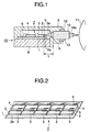
- Fig. 1 is a cross-sectional view of an optical print head of a first embodiment in the form of an LED print head.
- Fig. 2 is a perspective view showing an LED array unit 7.
- Fig. 3 illustrates a general construction of an electrophotographic printer to which the an optical print head of the first embodiment is applicable.
- An optical print head according to the present invention is an LED print head for use in an electrophotographic printer.
- a plurality of LED (Light Emitting Diode) array chips 2 are mounted in line on a circuit board 1.
- the LED array chips 2 emit light 3a in a lateral direction of an LED print head 13, from left to right in Fig. 1.
- the LED array chips 2 have light-emitting elements 3 disposed in its side surface 2a.
- the light-emitting elements 3 are spaced apart at predetermined intervals in accordance with the intended resolution of the LED print head 13. For example, light-emitting elements 3 are spaced apart 42.3 ⁇ m intervals if the resolution is 600 DPI (dot per inch).
- the number of LED chips 2 is determined by the width of a print medium. For example, about 40 chips are disposed on the circuit board 1.
- driver ICs 4 there are as many driver ICs 4 as there are LED array chips 2, each driver IC 4 being electrically connected by bonding wire 5 to a corresponding LED array chip 2 and driving it.
- the driver ICs 4 are also electrically connected by bonding wires 6 to the pattern traces on the circuit board 1.
- the circuit board 1, LED array chip 2, and driver IC 4 constitute an LED array unit 7.
- the LED array unit 7 is held on a base 8 made of, for example, aluminum, which base 8 serves as a heat sink and provides the overall rigidity of the LED print head.
- a supporting member 9 covers and holds a lens array 10 in the form of, for example, SELFOC lens array.
- the supporting member 9 may be made in one piece construction of of any suitable material.
- the lens array 10 includes an array of optical fibers. The optical fibers each extend in a direction parallel to the surface of the circuit board 1, and gathers the light emitted from the LED array chips 2 to illuminate the surface of a photosensitive drum 11.
- the lens array 10 is fixedly mounted by an adhesive 12.
- the supporting member 9 holds the LED array unit 7 and lens array 10 so that the focal point of the lens array 10 is on the light emitting surface of the light emitting element 3 of the LED array chips 2.
- the distance L between the lens array 10 and light-emitting elements 3 is equal to the focal length of the lens array 10.
- the LED print head 13 is of a thin construction extending in the direction of travel of the light 3a as shown in Fig. 1.
- Fig. 3 illustrate a general construction of an electrophotographic printer incorporating the optical print head 13 of the first embodiment.
- the photosensitive drum 11 is surrounded by the LED print head 13, a developer 14, transfer device 15, cleaner 16, discharging device 17, and charger 18.
- a hopping roller 19b feeds print paper one sheet at a time from a paper cassette 19a into a pair of feeding rollers 19c. Then the paper is transported to the transferring device 15 which transfers a toner image onto the paper. The paper is then fed between a heat rollers 19d for fixing. The paper is then pulled by a pair of discharge rollers 19e into an exit stacker 19f.
- the LED print head 13 is oriented so that the optical axis of the emitted light passes through the center O of the photosensitive drum 11.
- the LED print head 13 of thin construction occupies a minimum space in the circumferential direction of the photosensitive drum 11, lending itself to miniaturizing the photosensitive drum 11, hence a smaller sized electrophotographic printer.
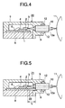
- Fig. 4 is a cross-sectional view of a first modification of the first embodiment.
- the LED array chips 2 are mounted on the driver ICs 4.
- the LED array chips 2 are connected to the corresponding driver ICs 4 so that the electrode pads of each LED array chip 2 are electrically and mechanically connected to the corresponding electrode pads by an anisotropically conductive film.
- the first modification provides the same advantages as the first embodiment and eliminates the need for wire bonding between the LED array chips 2 and driver ICs 4, simplifying the manufacture of the optical print head.
- Fig. 5 is a cross-sectional view of a second modification of the first embodiment.
- the circuit board 22 is assembled in an abutting relation with the lens array 10.
- the position of the lens array 10 relative to the LED array chip 2 is determined by the lateral dimension L of the circuit board 22.
- the distance L between the lens array 10 and the surface of light emitting elements 3 is selected to be equal to the focal length of the lens array 10.
- the position of the lens array 10 relative to the LED array chips 2 can be determined by the lateral dimension L of the circuit board. This eliminates the precision machining of the supporting member 9 which directly affects, in the first embodiment, the position of the lens array 10 relative to the LED array chips 2.
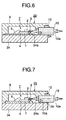
- Fig. 6 is a cross-sectional view of a third modification of the first embodiment.
- the LED array unit 7 and the lens array 10 are both mounted on a base 24 so that the positions of optical axes of the LED array chips 2 and lens array 10 are determined with respect to the base 24 in a direction shown by arrow A perpendicular to the optical axes.
- the base 24 may be made of any suitable material.
- the LED array unit 7 and lens array 10 are mounted on the same flat surface of the base 24 so that the height a of the light emitting elements 3 is the same as the height b of the optical axis 10e of the lens array 10. The rest of the construction is the same as that of the first embodiment.
- the base 24 serves as a reference height which is common to the LED array chips 2 and lens array 10, eliminating sources of cumulative dimensional errors resulting from the construction Figs. 1, and 4-5 in which the position of the LED array chips 2 relative to the lens array 10 is determined by a plurality of structural members such as the supporting member 9 and base 8.
- Fig. 7 is a cross-sectional view of a fourth modification of the first embodiment.
- the fourth modification differs from the third modification in that a spacer 26 is inserted between the base 24 and the lens array 10. The rest of the construction is the same as that of the third modification.
- Mounting the lens array 10 with the spacer 26 inserted between the base 24 and lens array 10 offers an additional degree of freedom in the thickness of the lens array 10 since the thickness of the spacer 26 can be varied in accordance with the thickness of the lens array 10.
- the spacer is advantageously used to adjust the height of the lens array 10 so that the the optical axis of the lens array is in line with the optical axis of the light-emitting LED array chips.
- the spacer 26 may be made of, for example, silicone rubber which offers intimate contact between the lens array 10 and base 24, providing an increased seal from the environment.
- Fig. 8 is a cross-sectional view of a fifth modification.
- a base 28 having a U-shaped cross section includes an upper plate 28b and a lower plate 28a and holds the LED array unit 7, supporting member 9, and lens array 10 between the upper and lower plates 28a and 28b.
- the base 28 is made of, for example, aluminum or steel. Inserted between the lower plate 28a and the lens array 10 is a spacer 26. The rest of the construction is the same as that of the fourth modification.
- the fifth embodiment provides a high overall rigidity of the optical print head, lending itself to miniaturizing the LED print head 27.
- Fig. 9 is a cross-sectional view of a sixth modification of the first embodiment.
- the sixth modification differs from the fifth modification in that a supporting member 30 is used in place of the supporting member 9.
- the supporting member 30 has two engaging portions 31 and 32.
- the engaging portion 31 has a bevel 31a and the engaging portion 32 has a hook 32a.
- the engaging portion 31 abuts a corner 10b of the lens array 10 and the engaging portion 32 abuts a corner 10c of the lens array 10, thereby holding the lens array 10 between the engaging portions 31 and 32.
- the base 28 has a lower plate 28a and an upper plate 28b which hold the lens array 10, supporting member 30 and spacer 26 therebetween in a sandwiched manner.
- the upper and lower plates 28b and 28a exert forces in such directions as to forcibly sandwich the lens array 10, supporting member 30, and spacer 26 together, the upper and lower plates cause the corner 10b of the lens array 10 to slide on the beveled surface 31a toward the contact surface 33, so that the corner 10c of the lens array 10 is urged against the hook 32a.
- the lens array 10 is firmly positioned in the direction of the optical axis 10e thereof, while also being urged against the contact surface 33 of the supporting member 30 to be firmly positioned in the direction perpendicular to the optical axis 10e of the lens array 10.
- Fig. 10 is a cross-sectional view of a seventh modification and Figs. 11A and 11B are perspective views showing the base and supporting member, respectively.
- a base 35 having a U-shaped cross section includes an upper plate 35b and a lower plate 35a which extend parallel to each other.
- the upper plate 35b is formed with two cutouts 36a and 36b that define a spring 36 therein.
- the spring 36 has a projection 37 projecting inwardly from the inner surface of the spring 36.
- the spring 36 is yieldably and resiliently deformable in a direction substantially normal to the the upper plate 35b.
- a supporting member 38 is formed with an I-shaped groove 39 in which when assembling, the projection 37 slidably moves.
- the projection 37 does not cause the spring 36 to significantly flex when the spring 36 slides on the flat bottom 39a but causes the spring 36 to flex progressively outwardly as the projection 37 climbs up the beveled bottom surface 39b. As the spring 36 flexes outwardly, the spring 36 exerts a larger pressing force which acts on the supporting member 38.
- the spring 36 may be formed at a plurality of locations in the base 35. The rest of the construction is the same as that of the sixth modification.
- the aforementioned construction where the spring 36 urges the supporting member 38, can conveniently absorb dimensional errors of the supporting member 38, lens array 10, and LED array unit 7 if the cumulative error is smaller than a predetermined value upon assembling these structural elements.
- the construction facilitates the assembly operation of the optical print head and ensures that the lens array 10 is firmly held by the base 35.
- the base 38 may be formed with a generally L-shaped groove 40 as shown in Fig. 12 in place of the I-shaped groove 39.
- the base 35 is fitted to the base 38 so that the projection 37 slides in the groove 40 and then slides laterally to climb a beveled surface 40b, the wall 40c of the L-shaped groove preventing the spring 36 from being pulled out.
- the base 35 is fastened to the base 38 so that the projection 37 will not climb down the beveled surface 40b.
- the projection 37 may climb fully the beveled slope 40b and pass onto the flat surface of the base 35 in which case the base 35 is fixed to the base 38 by some parts of the optical print head, not shown.
- Fig. 13 is a perspective view of an LED array unit of a second embodiment.
- Fig. 14 is a front view of Fig. 13 as seen in a direction shown by arrow A and Fig. 15 is a side view taken along lines XV-XV.
- the second embodiment differs from the first embodiment in the arrangement of the LED array chips.
- an LED array chip 42 includes light-emitting elements 3 disposed in its side surface.
- the LED array chips 42 are aligned in an upper row and a lower row in such a way that one LED chip 43A is mounted face up in the lower row between the adjacent LED array chips 43B mounted face down in the upper row.
- the LED array chips 43B in the upper row are held overlapping in part with the adjacent LED array chips 43A in the lower row.
- the light emitting elements 43a and 43b are offset from the center line of the side surface, so that the light emitting elements 43a and 43b are aligned substantially in line when the upper and lower LED array chips 43A and 43B are assembled on the circuit board 1 in the aforementioned alternate arrangement.
- the LED array chips 42a in the lower row are connected to the corresponding driver ICs 44a by bonding wires 5.
- the LED array chips 42a in the upper row are positioned such that they overlap the corresponding driver ICs 44b in part.
- Fig. 14 illustrates the LED array chip 42b in the upper row overlapping the LED array chip 42a in the lower row.
- Distance W1 is the center-to-center distance between the extreme light emitting element 43aa and its adjacent light emitting elements 43a of the LED array chip 42a.
- Distance W3 is the center-to-center distance between the extreme light emitting element 43ba and its adjacent light emitting element 43b of the LED array chip 42b.
- W1 is equal to W3.
- the distance W2 between the center of the extreme light emitting elements 43aa and the side surface of the LED array chip 42a is selected to be longer than the distance W1/2, so that the distance W4 can be adjusted to the distance W1 or W3 when the LED array chips 42b is held overlapping with the LED array chip 42a. It is to be noted that the LED array chip 42b is held by the driver IC 44b and is not in contact with the LED array chip 42a.
- Fig. 15 illustrates the LED array chip 42b in the upper row and the corresponding driver IC 44b.
- the LED array chip 42b has an electrode pattern 45 on its under side and the electrode pattern 45 is electrically connected via a bump electrode 46 of the driver IC 44b.
- the constructions of the lens array, base, and supporting member of the second embodiment may be the same as those of the first embodiment or the modifications of the first embodiment.
- the distance W2 is somewhat longer than the distance W1/2.
- the arrangement where the LED array chips in two rows are partly overlapping absorbs dimensional variations of the LED array chips to some extent. Therefore, the LED array chips may be scribed in as large a size as possible prior to during dicing process of a wafer, ensuring the manufacture of the LED array chips with high yield.
- Fig. 16 is a front view of an LED array chip which is a modification of the second embodiment.
- Fig. 17 is a perspective view of a wafer of the modified LED array chip.
- the upper corner 47a of the LED chip 42a in the lower row is removed by etching.
- the lower corner 47b of the LED chip 42b in the upper row is removed by etching. Removing the corners 47b and 47a of the upper and lower LED array chips 42b and 42a, respectively, allows the upper LED array chip 42b to be positioned at a vertically lower level in the arrangement shown in Fig. 16 than in arrangement shown in Fig. 14, so that the light emitting elements in the upper and lower LED array chips 42b and 42a can be aligned exactly on a single, straight line P-P'.
- Fig. 17 shows a wafer 48 of an LED array 49 before it is cut into individual LED array chips 42.
- the LED array 49 includes light-emitting elements 43 formed in line.
- the light-emitting elements 43 are to be connected via pads 45 to the driver ICs.
- Groove 51 are formed to extend perpendicular to a direction of the LED array 49 in which the light-emitting elements 43 are aligned, defining LED chips each of which has a predetermined number of light emitting elements 43.
- the grooves 51 are formed by etching during the photolithography process in which the light emitting elements 43 of the LED array chip 42 are formed, and can therefore be formed with a high dimensional accuracy.
- the LED array 49 is cut at the groove 51 to separate into individual LED array chips 42 at the dicing region 50.
- the aforementioned modification further improves the print quality of the optical print head of the second embodiment.
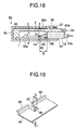
- Fig. 18 is a cross-sectional view of an LED print head of a third embodiment.
- the constructions of a supporting member 62 and a base 35 having a U-shaped cross section are the same as those of the supporting member 39 and the base 35 shown in Fig. 10.
- the base 35 is made of metal.
- the supporting member 62 may be made of any suitable material.
- An upper plate 35b of the base 35 is formed with a spring 36 therein similar to that in Fig. 11A and a projection 37 projecting inwardly of the base 35.
- the supporting member 62 has an engaging portion 63 at its free end.
- the engaging portions 63 has a beveled surface 63a downwardly extending toward the tip of the engaging portion 63.
- the spring 36 urges the engaging portion 63 against the lens array 10 when assembled.
- a positioning member 64 Inserted between the lens array 10 and a lower plate 35a is a positioning member 64.
- Fig. 19 is a fragmentary perspective view of the positioning member 64.
- the positioning member 64 is formed with a cutout 67 therein and projections 65 of an inverted L-shape at one end of the positioning member 64.
- Another projection 66 is formed at the end of the cutout 67 and rises in a direction in which the projections 65 rises from the positioning member 64.
- the L-shaped projections 65 engage a circuit board 1 pressing the side surface 1a and top surface of the circuit board 1 while the projection 66 abuts the side surface 10d of the lens array 10.
- the position of the lens array 10 relative to the LED array unit 7 is determined by the distance D between the projections 65 and 66, thereby ensuring that the focal point of the lens array 10 is on the light-emitting elements 3.
- the thickness t of the positioning member 64 is selected such that the optical axis 10e of the lens array 10 is at the same height from the lower plate 35a as the light-emitting elements 3 of the LED array chips 2.
- the projections 65 press the circuit board 1 against the lower plate 35a facilitating the heat transfer from the board 1 to lower plate 35a.
- the positioning member 64 is formed by bending a metal sheet having the same thickness as the spacer 26 of the fourth modification of the first embodiment.
- the positioning member 64 may also be formed, for example, by molding a material such as resin.
- Fig. 20 is a cross-sectional view of an LED print head 71 which is a modification of the third embodiment.
- Fig. 21 is a perspective view of a relevant part of the LED print head 71.
- a metal base 72 has a cross section of a generally U-shape and includes an upper plate 72b and a lower plate 72a.
- the lower plate 72a is formed with a U-shaped holes 77 therein which defines a spring 73.
- the spring 73 is formed with an inwardly projecting small projection 74 thereon.
- the board 75 has an exposed conductive pattern 76 which electrically contacts with the projection 74 of the spring 73.
- the rest of the construction of the LED print head 71 is the same as the third embodiment.
- a plurality of the springs 73 and projections 74 may be formed, as required.
- Static electricity resulting from the location of the optical print head close to the photosensitive drum may damage the optical print head. Static electricity may also cause discharge between an operator's body and the optical print head when the operator touches or gets close to the print head during maintenance.
- the exposed conductive pattern 76 in contact with the base 72 provides a path of static electricity developed in the base 72 to the ground, thereby preventing the damage of the optical print head.
- Fig. 22 is a cross-sectional view of an LED print head of a fourth embodiment and Fig. 23 is a fragmentary cross-sectional perspective view of a lower supporting member used in the fourth embodiment.
- a metal base 82 having a U-shaped cross section includes upper and lower plates 82b and 82a, which hold an upper supporting member 83 and a lower supporting member 84 in a sandwiched relation.
- the lower supporting member 84 includes an LED support 84a and a lens support 84b.
- the upper supporting member 83 engages upper and side surfaces of the circuit board 1 of the LED array unit 7 and cooperates with the LED support 84a to firmly hold the LED array unit 7 therebetween in a sandwiched relation.
- the upper supporting member 83 engages a lens array 10 and cooperates with the lens support 84b to firmly hold the lens array 10 therebetween in a sandwiched relation.
- the LED support 84a is made of, for example, aluminum alloy and has a groove 86 formed therein.
- the lens support 84b is made by molding a resin and has a projection 85. The projection 85 fits into the groove 86 so that the LED support 84a is firmly connected to the lens support 84b into an integral construction.
- the LED support 84a made of aluminum alloy provides efficient heat transfer from the circuit board 1 to the base 82, improving heat dissipation, and provides a higher rigidity preventing the deformation of the lens support 84b.
- the lens support 84b is formed with a projection 87 thereon which serves to position the lens array 10 in the direction of its optical axis.
- the rod lens 10 is bonded to the lens support 84b by an adhesive 12.
- the lens support 84b is made of a material such as phenol resin, epoxy resin, or unsaturated polyester resin.
- the use of resin to form the lens support has the following advantage.
- the lens support 84b is closer to the photosensitive drum 11 than the LED support 84a when assembled in the electrophotographic printer.
- the surface of the photosensitive drum 11 is charged and then an electrostatic latent image is formed in the charged surface. If metal is in proximity to the charged surface, then an electric field is developed between the metal and the charged surface of the photosensitive drum 11.
- static electricity is detrimental to the print head frame and therefore the metal material of the frame is usually grounded.
- the metal construction is always at zero volts so that an electric field is necessarily developed between the print head frame and the photosensitive drum 11.
- the toner particles may adhere to the LED print head with the aid of the electric field between the photosensitive drum 11 and the print head frame.
- the toner particles adhering to the LED print head interfere with the light which illuminates the photosensitive drum 11 during printing operation, leading to poor print quality. Therefore, forming the lens support 84b of resin rather than metal, effectively prevents deterioration of print quality.
- the LED support 84a and lens support 84b are made of materials having substantially the same coefficient of thermal expansion.
- the substantially the same coefficient of thermal expansion prevents deformation of the overall construction of the lower supporting member 84 which is encountered if the LED support 84a and lens support 84b have considerably different coefficients of thermal expansion.
Abstract
Description
- The present invention relates to an optical print head used in electrophotographic recording apparatuses such as an electrophotographic printer and a copying machine, and more particularly to the construction of the optical print head in which light illuminates a latent image-bearing body to form an electrostatic latent image therein.
- Electrophotographic recording apparatuses including electrophotographic printers incorporate an optical head, charger, developer, transferring device, and cleaner, disposed around a photosensitive drum that bears a latent image therein. The optical print head incorporates a light source such as lasers, LEDs, and liquid crystal devices. For example, with an optical print head using LEDs, LED array chips are arranged in line on a printed circuit board, each array chip having a plurality of LEDs fabricated therein. Driver ICs which drive the LED array chips are also arranged in line parallel to the LED array chips. Electrical connections between the LED array chips and driver ICs are made by wire bonding. The LED array chips emit light in a direction normal to the component side, the light traveling toward a lens array such as SELFOC lens array. The lens array gathers the light emitted from the LED chips and directs the gathered light to illuminate the photosensitive drum, thereby forming a latent image on the photosensitive drum.
- The aforementioned optical print head is of the construction where the LED array chips emit light in a direction normal to the component side of the circuit board. This construction requires a considerable width which occupies a relatively large space when mounted around the photosensitive drum. Therefore, the photosensitive drum should have a large diameter so that the optical print head, can be comfortably mounted together with other components around the photosensitive drum. A larger diameter of the photosensitive drum is an obstacle to miniaturizing of the apparatus.
- An object of the present invention is to provide an optical print head for use in an electrophotographic printer which occupies a minimum space in the direction of circumference of the photosensitive drum.
- The object of the invention is achieved by an optical print head having a light-emitting array chip (2), driver IC (4) that drives the light-emitting array chip (2), lens array (10), and circuit board (1) to which the light-emitting array chip (2) and driver IC are mounted. The light-emitting array chip (2) has light emitting elements (43) therein aligned in line. The driver IC (4) electrically is connected to the light-emitting array chip (2), and electrically drives the light-emitting array chip (2) to emit light. The lens array (10) gathers the light emitted from the light-emitting elements (43) and emanates the gathered light onto the photosensitive drum. The lens array (10) has a focal point and is positioned relative to the light-emitting array chip (2) so that the focal point of the lens array (10) is on the light-emitting elements (43). The circuit board (1, 75) has a surface on which the light-emitting array chip (2) and the driver IC (4) are mounted. The circuit board (1, 75) supports the light-emitting array chip (2) so that the light-emitting elements (43) emit the light in a direction parallel to the surface of the circuit board (1, 75).
- Further scope of applicability of the present invention will become apparent from the detailed description given hereinafter. However, it should be understood that the detailed description and specific examples, while indicating preferred embodiments of the invention, are given by way of illustration only, since various changes and modifications within the spirit and scope of the invention will become apparent to those skilled in the art from this detailed description.
- The present invention will become more fully understood from the detailed description given hereinbelow and the accompanying drawings which are given by way of illustration only, and thus are not limitative of the present invention, and wherein:
- Fig. 1 is a cross-sectional view of an LED print head of a first embodiment;
- Fig. 2 is a perspective view showing an LED array unit of the first embodiment;
- Fig. 3 illustrates a general construction of an electrophotographic printer of the first embodiment;
- Fig. 4 is a cross-sectional view of a first modification of the first embodiment;
- Fig. 5 is a cross-sectional view of a second modification of the first embodiment;
- Fig. 6 is a cross-sectional vie of a third modification of the first embodiment;
- Fig. 7 is a cross-sectional view of a fourth modification of the first embodiment;
- Fig. 8 is a cross-sectional view of a fifth modification of the first embodiment;
- Fig. 9 is a cross-sectional view of a sixth modification of the first embodiment;
- Fig. 10 is a cross-sectional view of a seventh modification of the first embodiment;
- Fig. 11A is a perspective view showing the base;
- Fig. 11B is a perspective view showing the supporting member of the seventh modification;
- Fig. 12 illustrates a modification of the supporting member in Fig. 11B;
- Fig. 13 is a perspective view of an LED array unit of a second embodiment;
- Fig. 14 is a front view of Fig. 13 as seen in a direction shown by arrow A;
- Fig. 15 is a side view of Fig. 13 taken along lines XV-XV;
- Fig. 16 is a front view of an LED array chip which is a modification of the second embodiment;
- Fig. 17 is a perspective view of a wafer of the modified LED array chip;
- Fig. 18 is a cross-sectional view of an LED print head of a third embodiment;
- Fig. 19 is a perspective view of the positioning member of the third embodiment;
- Fig. 20 is a cross-sectional view of a modified LED print head of the third embodiment;
- Fig. 21 is a perspective view of a relevant part of the
LED print head 71 of the third embodiment; - Fig. 22 is a cross-sectional view of an LED print head of a fourth embodiment; and
- Fig. 23 is a cross-sectional perspective view of a lower supporting member of the fourth embodiment.
- The preferred embodiments of the present invention will be described with reference to the accompanying drawings. Fig. 1 is a cross-sectional view of an optical print head of a first embodiment in the form of an LED print head. Fig. 2 is a perspective view showing an
LED array unit 7. Fig. 3 illustrates a general construction of an electrophotographic printer to which the an optical print head of the first embodiment is applicable. - An optical print head according to the present invention is an LED print head for use in an electrophotographic printer.
- Referring to Fig. 1 and 2, a plurality of LED (Light Emitting Diode)
array chips 2 are mounted in line on acircuit board 1. TheLED array chips 2 emit light 3a in a lateral direction of anLED print head 13, from left to right in Fig. 1. TheLED array chips 2 have light-emitting elements 3 disposed in itsside surface 2a. The light-emittingelements 3 are spaced apart at predetermined intervals in accordance with the intended resolution of theLED print head 13. For example, light-emitting elements 3 are spaced apart 42.3 µm intervals if the resolution is 600 DPI (dot per inch). The number ofLED chips 2 is determined by the width of a print medium. For example, about 40 chips are disposed on thecircuit board 1. There are asmany driver ICs 4 as there areLED array chips 2, eachdriver IC 4 being electrically connected bybonding wire 5 to a correspondingLED array chip 2 and driving it. Thedriver ICs 4 are also electrically connected bybonding wires 6 to the pattern traces on thecircuit board 1. Thecircuit board 1,LED array chip 2, anddriver IC 4 constitute anLED array unit 7. - The
LED array unit 7 is held on abase 8 made of, for example, aluminum, whichbase 8 serves as a heat sink and provides the overall rigidity of the LED print head. A supportingmember 9 covers and holds alens array 10 in the form of, for example, SELFOC lens array. The supportingmember 9 may be made in one piece construction of of any suitable material. Thelens array 10 includes an array of optical fibers. The optical fibers each extend in a direction parallel to the surface of thecircuit board 1, and gathers the light emitted from theLED array chips 2 to illuminate the surface of aphotosensitive drum 11. Thelens array 10 is fixedly mounted by an adhesive 12. The supportingmember 9 holds theLED array unit 7 andlens array 10 so that the focal point of thelens array 10 is on the light emitting surface of thelight emitting element 3 of the LED array chips 2. In other words, the distance L between thelens array 10 and light-emittingelements 3 is equal to the focal length of thelens array 10. TheLED print head 13 is of a thin construction extending in the direction of travel of the light 3a as shown in Fig. 1. - Fig. 3 illustrate a general construction of an electrophotographic printer incorporating the
optical print head 13 of the first embodiment. Referring to Fig. 3, Thephotosensitive drum 11 is surrounded by theLED print head 13, adeveloper 14,transfer device 15, cleaner 16, dischargingdevice 17, andcharger 18. - A hopping
roller 19b feeds print paper one sheet at a time from apaper cassette 19a into a pair of feedingrollers 19c. Then the paper is transported to the transferringdevice 15 which transfers a toner image onto the paper. The paper is then fed between aheat rollers 19d for fixing. The paper is then pulled by a pair ofdischarge rollers 19e into anexit stacker 19f. - The
LED print head 13 is oriented so that the optical axis of the emitted light passes through the center O of thephotosensitive drum 11. TheLED print head 13 of thin construction occupies a minimum space in the circumferential direction of thephotosensitive drum 11, lending itself to miniaturizing thephotosensitive drum 11, hence a smaller sized electrophotographic printer. - Fig. 4 is a cross-sectional view of a first modification of the first embodiment. Referring to Fig. 4, the
LED array chips 2 are mounted on thedriver ICs 4. TheLED array chips 2 are connected to the correspondingdriver ICs 4 so that the electrode pads of eachLED array chip 2 are electrically and mechanically connected to the corresponding electrode pads by an anisotropically conductive film. - The first modification provides the same advantages as the first embodiment and eliminates the need for wire bonding between the
LED array chips 2 anddriver ICs 4, simplifying the manufacture of the optical print head. - Fig. 5 is a cross-sectional view of a second modification of the first embodiment. Referring to Fig. 5, the
circuit board 22 is assembled in an abutting relation with thelens array 10. In other words, the position of thelens array 10 relative to theLED array chip 2 is determined by the lateral dimension L of thecircuit board 22. The distance L between thelens array 10 and the surface oflight emitting elements 3 is selected to be equal to the focal length of thelens array 10. - In the second modification, the position of the
lens array 10 relative to theLED array chips 2 can be determined by the lateral dimension L of the circuit board. This eliminates the precision machining of the supportingmember 9 which directly affects, in the first embodiment, the position of thelens array 10 relative to the LED array chips 2. - Fig. 6 is a cross-sectional view of a third modification of the first embodiment. Referring to Fig. 6, the
LED array unit 7 and thelens array 10 are both mounted on a base 24 so that the positions of optical axes of theLED array chips 2 andlens array 10 are determined with respect to the base 24 in a direction shown by arrow A perpendicular to the optical axes. The base 24 may be made of any suitable material. TheLED array unit 7 andlens array 10 are mounted on the same flat surface of the base 24 so that the height a of thelight emitting elements 3 is the same as the height b of theoptical axis 10e of thelens array 10. The rest of the construction is the same as that of the first embodiment. - In the third embodiment, the
base 24 serves as a reference height which is common to theLED array chips 2 andlens array 10, eliminating sources of cumulative dimensional errors resulting from the construction Figs. 1, and 4-5 in which the position of theLED array chips 2 relative to thelens array 10 is determined by a plurality of structural members such as the supportingmember 9 andbase 8. - Fig. 7 is a cross-sectional view of a fourth modification of the first embodiment. Referring to Fig. 7, the fourth modification differs from the third modification in that a
spacer 26 is inserted between the base 24 and thelens array 10. The rest of the construction is the same as that of the third modification. - Mounting the
lens array 10 with thespacer 26 inserted between the base 24 andlens array 10 offers an additional degree of freedom in the thickness of thelens array 10 since the thickness of thespacer 26 can be varied in accordance with the thickness of thelens array 10. The spacer is advantageously used to adjust the height of thelens array 10 so that the the optical axis of the lens array is in line with the optical axis of the light-emitting LED array chips. - The
spacer 26 may be made of, for example, silicone rubber which offers intimate contact between thelens array 10 andbase 24, providing an increased seal from the environment. - Fig. 8 is a cross-sectional view of a fifth modification. Referring to Fig. 8, a
base 28 having a U-shaped cross section includes anupper plate 28b and alower plate 28a and holds theLED array unit 7, supportingmember 9, andlens array 10 between the upper andlower plates base 28 is made of, for example, aluminum or steel. Inserted between thelower plate 28a and thelens array 10 is aspacer 26. The rest of the construction is the same as that of the fourth modification. - Holding the
LED array unit 7, supportingmember 9, andlens array 10 in a "shell-like construction" of the base 28 having a U-shaped cross section, the fifth embodiment provides a high overall rigidity of the optical print head, lending itself to miniaturizing theLED print head 27. - Fig. 9 is a cross-sectional view of a sixth modification of the first embodiment. Referring to Fig. 9, the sixth modification differs from the fifth modification in that a supporting
member 30 is used in place of the supportingmember 9. The supportingmember 30 has twoengaging portions portion 31 has abevel 31a and the engagingportion 32 has ahook 32a. The engagingportion 31 abuts acorner 10b of thelens array 10 and the engagingportion 32 abuts acorner 10c of thelens array 10, thereby holding thelens array 10 between the engagingportions base 28 has alower plate 28a and anupper plate 28b which hold thelens array 10, supportingmember 30 andspacer 26 therebetween in a sandwiched manner. When the upper andlower plates lens array 10, supportingmember 30, andspacer 26 together, the upper and lower plates cause thecorner 10b of thelens array 10 to slide on thebeveled surface 31a toward thecontact surface 33, so that thecorner 10c of thelens array 10 is urged against thehook 32a. Thus, thelens array 10 is firmly positioned in the direction of theoptical axis 10e thereof, while also being urged against thecontact surface 33 of the supportingmember 30 to be firmly positioned in the direction perpendicular to theoptical axis 10e of thelens array 10. - The need for bonding the
lens array 10 by an adhesive is eliminated by the aforementioned construction where thelens array 10 is fixedly mounted in intimate contact with engagingportions LED array unit 7 and the supportingmember 30 into the base 28 automatically determines th position of thelens array 10, simplifying the assembly of an LED print head. - Fig. 10 is a cross-sectional view of a seventh modification and Figs. 11A and 11B are perspective views showing the base and supporting member, respectively. A base 35 having a U-shaped cross section includes an
upper plate 35b and alower plate 35a which extend parallel to each other. Theupper plate 35b is formed with twocutouts spring 36 therein. Thespring 36 has aprojection 37 projecting inwardly from the inner surface of thespring 36. Thespring 36 is yieldably and resiliently deformable in a direction substantially normal to the theupper plate 35b. A supportingmember 38 is formed with an I-shapedgroove 39 in which when assembling, theprojection 37 slidably moves. Theprojection 37 does not cause thespring 36 to significantly flex when thespring 36 slides on theflat bottom 39a but causes thespring 36 to flex progressively outwardly as theprojection 37 climbs up the beveledbottom surface 39b. As thespring 36 flexes outwardly, thespring 36 exerts a larger pressing force which acts on the supportingmember 38. Thespring 36 may be formed at a plurality of locations in thebase 35. The rest of the construction is the same as that of the sixth modification. - The aforementioned construction where the
spring 36 urges the supportingmember 38, can conveniently absorb dimensional errors of the supportingmember 38,lens array 10, andLED array unit 7 if the cumulative error is smaller than a predetermined value upon assembling these structural elements. The construction facilitates the assembly operation of the optical print head and ensures that thelens array 10 is firmly held by thebase 35. - The base 38 may be formed with a generally L-shaped
groove 40 as shown in Fig. 12 in place of the I-shapedgroove 39. When assembling, thebase 35 is fitted to the base 38 so that theprojection 37 slides in thegroove 40 and then slides laterally to climb abeveled surface 40b, thewall 40c of the L-shaped groove preventing thespring 36 from being pulled out. Then, thebase 35 is fastened to the base 38 so that theprojection 37 will not climb down thebeveled surface 40b. Theprojection 37 may climb fully thebeveled slope 40b and pass onto the flat surface of the base 35 in which case thebase 35 is fixed to thebase 38 by some parts of the optical print head, not shown. - Fig. 13 is a perspective view of an LED array unit of a second embodiment. Fig. 14 is a front view of Fig. 13 as seen in a direction shown by arrow A and Fig. 15 is a side view taken along lines XV-XV. The second embodiment differs from the first embodiment in the arrangement of the LED array chips.
- Referring to Fig. 13, an
LED array chip 42 includes light-emittingelements 3 disposed in its side surface. The LED array chips 42 are aligned in an upper row and a lower row in such a way that oneLED chip 43A is mounted face up in the lower row between the adjacentLED array chips 43B mounted face down in the upper row. The LED array chips 43B in the upper row are held overlapping in part with the adjacentLED array chips 43A in the lower row. Thelight emitting elements light emitting elements LED array chips circuit board 1 in the aforementioned alternate arrangement. TheLED array chips 42a in the lower row are connected to the correspondingdriver ICs 44a bybonding wires 5. TheLED array chips 42a in the upper row are positioned such that they overlap the correspondingdriver ICs 44b in part. - Fig. 14 illustrates the
LED array chip 42b in the upper row overlapping theLED array chip 42a in the lower row. Distance W1 is the center-to-center distance between the extreme light emitting element 43aa and its adjacentlight emitting elements 43a of theLED array chip 42a. Distance W3 is the center-to-center distance between the extreme light emitting element 43ba and its adjacentlight emitting element 43b of theLED array chip 42b. W1 is equal to W3. The distance W2 between the center of the extreme light emitting elements 43aa and the side surface of theLED array chip 42a is selected to be longer than the distance W1/2, so that the distance W4 can be adjusted to the distance W1 or W3 when theLED array chips 42b is held overlapping with theLED array chip 42a. It is to be noted that theLED array chip 42b is held by thedriver IC 44b and is not in contact with theLED array chip 42a. - Fig. 15 illustrates the
LED array chip 42b in the upper row and the correspondingdriver IC 44b. TheLED array chip 42b has anelectrode pattern 45 on its under side and theelectrode pattern 45 is electrically connected via abump electrode 46 of thedriver IC 44b. - The constructions of the lens array, base, and supporting member of the second embodiment may be the same as those of the first embodiment or the modifications of the first embodiment.
- Selecting the distance W2 to be somewhat longer than the distance W1/2 allows adjustment of the center-to-center distance W4 between the light-emitting elements 43aa and 43ba to the distance W1. This makes it possible to manufacture LED print heads having a high resolution while still maintaining the same print quality. The arrangement where the LED array chips in two rows are partly overlapping absorbs dimensional variations of the LED array chips to some extent. Therefore, the LED array chips may be scribed in as large a size as possible prior to during dicing process of a wafer, ensuring the manufacture of the LED array chips with high yield.
- Fig. 16 is a front view of an LED array chip which is a modification of the second embodiment. Fig. 17 is a perspective view of a wafer of the modified LED array chip. Referring to Fig. 16, the
upper corner 47a of theLED chip 42a in the lower row is removed by etching. Likewise, thelower corner 47b of theLED chip 42b in the upper row is removed by etching. Removing thecorners LED array chips LED array chip 42b to be positioned at a vertically lower level in the arrangement shown in Fig. 16 than in arrangement shown in Fig. 14, so that the light emitting elements in the upper and lowerLED array chips - Fig. 17 shows a
wafer 48 of anLED array 49 before it is cut into individual LED array chips 42. TheLED array 49 includes light-emittingelements 43 formed in line. The light-emittingelements 43 are to be connected viapads 45 to the driver ICs.Groove 51 are formed to extend perpendicular to a direction of theLED array 49 in which the light-emittingelements 43 are aligned, defining LED chips each of which has a predetermined number oflight emitting elements 43. Thegrooves 51 are formed by etching during the photolithography process in which thelight emitting elements 43 of theLED array chip 42 are formed, and can therefore be formed with a high dimensional accuracy. TheLED array 49 is cut at thegroove 51 to separate into individual LED array chips 42 at thedicing region 50. - The aforementioned modification, further improves the print quality of the optical print head of the second embodiment.
- Fig. 18 is a cross-sectional view of an LED print head of a third embodiment. The constructions of a supporting
member 62 and a base 35 having a U-shaped cross section are the same as those of the supportingmember 39 and the base 35 shown in Fig. 10. Thebase 35 is made of metal. The supportingmember 62 may be made of any suitable material. Anupper plate 35b of thebase 35 is formed with aspring 36 therein similar to that in Fig. 11A and aprojection 37 projecting inwardly of thebase 35. The supportingmember 62 has an engagingportion 63 at its free end. The engagingportions 63 has abeveled surface 63a downwardly extending toward the tip of the engagingportion 63. Thespring 36 urges the engagingportion 63 against thelens array 10 when assembled. - Inserted between the
lens array 10 and alower plate 35a is a positioningmember 64. Fig. 19 is a fragmentary perspective view of the positioningmember 64. Referring to Fig. 19, the positioningmember 64 is formed with acutout 67 therein andprojections 65 of an inverted L-shape at one end of the positioningmember 64. Anotherprojection 66 is formed at the end of thecutout 67 and rises in a direction in which theprojections 65 rises from the positioningmember 64. As shown in Fig. 18, when assembled to theLED print head 61, the L-shapedprojections 65 engage acircuit board 1 pressing theside surface 1a and top surface of thecircuit board 1 while theprojection 66 abuts the side surface 10d of thelens array 10. In other words, the position of thelens array 10 relative to theLED array unit 7 is determined by the distance D between theprojections lens array 10 is on the light-emittingelements 3. - The thickness t of the positioning
member 64 is selected such that theoptical axis 10e of thelens array 10 is at the same height from thelower plate 35a as the light-emittingelements 3 of the LED array chips 2. Theprojections 65 press thecircuit board 1 against thelower plate 35a facilitating the heat transfer from theboard 1 tolower plate 35a. - The positioning
member 64 is formed by bending a metal sheet having the same thickness as thespacer 26 of the fourth modification of the first embodiment. The positioningmember 64 may also be formed, for example, by molding a material such as resin. - Fig. 20 is a cross-sectional view of an
LED print head 71 which is a modification of the third embodiment. Fig. 21 is a perspective view of a relevant part of theLED print head 71. Ametal base 72 has a cross section of a generally U-shape and includes anupper plate 72b and alower plate 72a. Thelower plate 72a is formed with aU-shaped holes 77 therein which defines aspring 73. Thespring 73 is formed with an inwardly projectingsmall projection 74 thereon. When theLED print head 71 is assembled, theprojection 74 abuts theboard 75 of theLED array unit 7 and yieldably flexes outwardly while urging thecircuit board 75. - The
board 75 has an exposedconductive pattern 76 which electrically contacts with theprojection 74 of thespring 73. The rest of the construction of theLED print head 71 is the same as the third embodiment. A plurality of thesprings 73 andprojections 74 may be formed, as required. - Static electricity resulting from the location of the optical print head close to the photosensitive drum may damage the optical print head. Static electricity may also cause discharge between an operator's body and the optical print head when the operator touches or gets close to the print head during maintenance.
- The exposed
conductive pattern 76 in contact with thebase 72 provides a path of static electricity developed in the base 72 to the ground, thereby preventing the damage of the optical print head. - Fig. 22 is a cross-sectional view of an LED print head of a fourth embodiment and Fig. 23 is a fragmentary cross-sectional perspective view of a lower supporting member used in the fourth embodiment.
- A
metal base 82 having a U-shaped cross section includes upper andlower plates member 83 and a lower supportingmember 84 in a sandwiched relation. The lower supportingmember 84 includes anLED support 84a and alens support 84b. The upper supportingmember 83 engages upper and side surfaces of thecircuit board 1 of theLED array unit 7 and cooperates with theLED support 84a to firmly hold theLED array unit 7 therebetween in a sandwiched relation. The upper supportingmember 83 engages alens array 10 and cooperates with thelens support 84b to firmly hold thelens array 10 therebetween in a sandwiched relation. - The
LED support 84a is made of, for example, aluminum alloy and has agroove 86 formed therein. Thelens support 84b is made by molding a resin and has aprojection 85. Theprojection 85 fits into thegroove 86 so that theLED support 84a is firmly connected to thelens support 84b into an integral construction. - The
LED support 84a made of aluminum alloy provides efficient heat transfer from thecircuit board 1 to thebase 82, improving heat dissipation, and provides a higher rigidity preventing the deformation of thelens support 84b. - The
lens support 84b is formed with aprojection 87 thereon which serves to position thelens array 10 in the direction of its optical axis. Therod lens 10 is bonded to thelens support 84b by an adhesive 12. Thelens support 84b is made of a material such as phenol resin, epoxy resin, or unsaturated polyester resin. - The use of resin to form the lens support has the following advantage. The
lens support 84b is closer to thephotosensitive drum 11 than theLED support 84a when assembled in the electrophotographic printer. The surface of thephotosensitive drum 11 is charged and then an electrostatic latent image is formed in the charged surface. If metal is in proximity to the charged surface, then an electric field is developed between the metal and the charged surface of thephotosensitive drum 11. Generally, static electricity is detrimental to the print head frame and therefore the metal material of the frame is usually grounded. As a result, the metal construction is always at zero volts so that an electric field is necessarily developed between the print head frame and thephotosensitive drum 11. If toner particles are left on thephotosensitive drum 11, the toner particles may adhere to the LED print head with the aid of the electric field between thephotosensitive drum 11 and the print head frame. The toner particles adhering to the LED print head interfere with the light which illuminates thephotosensitive drum 11 during printing operation, leading to poor print quality. Therefore, forming thelens support 84b of resin rather than metal, effectively prevents deterioration of print quality. - The
LED support 84a andlens support 84b are made of materials having substantially the same coefficient of thermal expansion. The substantially the same coefficient of thermal expansion prevents deformation of the overall construction of the lower supportingmember 84 which is encountered if theLED support 84a andlens support 84b have considerably different coefficients of thermal expansion. - The invention being thus described, it will be obvious that the same may be varied in many ways. Such variations are not to be regarded as a departure from the spirit and scope of the invention, and all such modifications as would be obvious to one skilled in the art are intended to be included within the scope of the following claims.
Claims (14)
- An optical print head, comprising:a light-emitting array chip (2) having light emitting elements (43);a driver IC (4) electrically driving said light-emitting array chip (2) to emit light;a lens array (10) having a focal point, said lens array (10) gathering the light emitted from said light-emitting elements (43) and emanating the gathered light, said lens array (10) being positioned relative to said light-emitting array chip (2) so that the focal point of said lens array (10) is on the light-emitting elements (43); anda circuit board (1, 75) having a surface to which said light-emitting array chip (2) and said driver IC (4) are mounted, said circuit board (1, 75) supporting said light-emitting array chip (2) so that said light-emitting elements (43) emit the light in a first direction parallel to the surface of said circuit board (1, 75).
- The optical print head according to Claim 1, wherein there are provided a plurality of said light-emitting array chips (2) and a plurality of said driver ICs, said plurality of light-emitting array chips (2) being aligned straight in a second direction perpendicular to the first direction and parallel to the surface of said circuit board.
- The optical print head according to Claim 2, wherein said light-emitting array chips (2) are mounted on said driver ICs, each light-emitting array chip (2) being electrically and mechanically connected to the corresponding driver IC.
- The optical print head according to Claim 2, wherein said light-emitting array chips (2) are positioned relative to a front edge of said circuit board such that the focal point of said lens array (10) is on the light-emitting elements (43) when the front edge of said circuit board is positioned to abut said lens array.
- The optical print head according to Claim 2 further including a reference member (24, 28, 35, 72), wherein said light-emitting array chips (2) and said lens array (10) are positioned relative to said reference member in a third direction normal to the surface of said circuit board.
- The optical print head according to Claim 5 further including a spacer (26) inserted between said reference member (24, 28, 35, 72) and said lens array (10) so as to adjust the position of the optical axis of said lens array (10) in said third direction.
- The optical print head according to Claim 5, wherein said reference member (28, 35, 72) has a first plate (28a, 35a, 72a) and a second plate (28b, 35b, 72b) opposing each other, and said circuit board (1) and said lens array (10) are sandwiched between said first and second plates, said light-emitting array chips (2) and said lens array (10) being positioned relative to said first plate.
- The optical print head according to Claim 7, wherein said reference member has a spring which urges said lens array so as to firmly hold said lens array (10) between said first and second plates.
- The optical print head according to Claim 2 further including a positioning member (64), wherein said positioning member (64) positions said lens array (10) relative to said light-emitting elements (43) in the third direction.
- The optical print head according to Claim 9, wherein said circuit board (75) has a conductive pattern (76) formed thereon, and said reference member is connected to ground and has an electrical contact (74) in contact with the conductive pattern (76).
- The optical print head according to Claim 2 further including a supporting member (84) having a first support (84a) made of a metal and a second support (84b) made of a resin, said first support (84a) supporting said circuit board (1) and said second support (84b) supporting said lens array (10).
- The optical print head according to Claim 11, wherein said first support (84a) is secured to said second support (84b), said first and second supports (84a, 84b) having a substantially same coefficient of thermal expansion.
- The optical print head according to Claim 1, wherein there are provided a plurality of said light-emitting array chips, each of said light-emitting array chips having a side surface with a center line extending parallel to the second direction, said light emitting elements being offset from the center line, wherein said light emitting array chips are arranged in an upper row and in a lower row, the chips in the lower row being mounted face up and the chips in the upper row being mounted face down, the chips in the upper row overlapping with adjacent chips in the lower row such that the light-emitting elements are equally spaced in the second direction.
- The optical print head according to Claim 13, wherein said light-emitting array chips have corner portions cut away and said light-emitting array chips in the upper row are positioned relative to said light-emitting array chips in the lower row such that the light-emitting elements are in a single line extending in the second direction.
Applications Claiming Priority (6)
| Application Number | Priority Date | Filing Date | Title |
|---|---|---|---|
| JP2537696 | 1996-02-13 | ||
| JP25376/96 | 1996-02-13 | ||
| JP2537696 | 1996-02-13 | ||
| JP25650196 | 1996-09-27 | ||
| JP256501/96 | 1996-09-27 | ||
| JP25650196A JPH09277595A (en) | 1996-02-13 | 1996-09-27 | Photoprinting head |
Publications (3)
| Publication Number | Publication Date |
|---|---|
| EP0790132A2 true EP0790132A2 (en) | 1997-08-20 |
| EP0790132A3 EP0790132A3 (en) | 1998-05-27 |
| EP0790132B1 EP0790132B1 (en) | 2000-05-10 |
Family
ID=26362972
Family Applications (1)
| Application Number | Title | Priority Date | Filing Date |
|---|---|---|---|
| EP97102014A Expired - Lifetime EP0790132B1 (en) | 1996-02-13 | 1997-02-06 | Optical print head |
Country Status (3)
| Country | Link |
|---|---|
| EP (1) | EP0790132B1 (en) |
| JP (1) | JPH09277595A (en) |
| DE (1) | DE69701903T2 (en) |
Cited By (7)
| Publication number | Priority date | Publication date | Assignee | Title |
|---|---|---|---|---|
| EP1142723A3 (en) * | 2000-04-06 | 2002-03-06 | Nippon Sheet Glass Co., Ltd. | Optical write head, and method of assembling the same |
| WO2007124737A1 (en) * | 2006-05-03 | 2007-11-08 | Osram Opto Semiconductors Gmbh | Radiation-emitting semiconductor body with carrier substrate and method for the production thereof |
| DE102005041751B4 (en) * | 2004-09-30 | 2012-05-16 | Heidelberger Druckmaschinen Ag | Apparatus for imaging on a recording material |
| CN103072385A (en) * | 2011-09-14 | 2013-05-01 | 株式会社理光 | Optical printing head and imaging device |
| US20200313400A1 (en) * | 2017-12-13 | 2020-10-01 | Sony Corporation | Method of manufacturing light-emitting module, light-emitting module, and device |
| CN112083632A (en) * | 2020-09-22 | 2020-12-15 | 深圳市先地图像科技有限公司 | Digital projection maskless exposure device and method based on LED array |
| WO2023207988A1 (en) * | 2022-04-29 | 2023-11-02 | 华为技术有限公司 | Led light-emitting module, led print head, and led printer |
Families Citing this family (5)
| Publication number | Priority date | Publication date | Assignee | Title |
|---|---|---|---|---|
| JP2001162862A (en) * | 1999-12-13 | 2001-06-19 | Kyocera Corp | Optical printer head |
| JP5363942B2 (en) * | 2009-10-23 | 2013-12-11 | 株式会社沖データ | Exposure apparatus and image forming apparatus |
| JP6621591B2 (en) * | 2015-03-31 | 2019-12-18 | 株式会社沖データ | Rod lens array unit, rod lens array unit manufacturing method, LED print head, image sensor head, image forming apparatus, and image reading apparatus |
| JP2018016009A (en) * | 2016-07-29 | 2018-02-01 | 株式会社沖データ | Exposure device and light receiving device |
| JP2020163601A (en) * | 2019-03-28 | 2020-10-08 | 京セラ株式会社 | Optical print head and image formation apparatus having the same |
Citations (6)
| Publication number | Priority date | Publication date | Assignee | Title |
|---|---|---|---|---|
| JPS61189965A (en) * | 1985-02-19 | 1986-08-23 | Oki Electric Ind Co Ltd | Optical printing head |
| US4951064A (en) * | 1989-05-15 | 1990-08-21 | Westinghouse Electric Corp. | Thin film electroluminescent edge emitter assembly and integral packaging |
| EP0504575A2 (en) * | 1991-03-22 | 1992-09-23 | Eastman Kodak Company | Light-emitting diode device |
| US5179396A (en) * | 1991-02-21 | 1993-01-12 | Samsung Electronics Co., Ltd. | Light emitting diode print head |
| EP0601485A2 (en) * | 1992-12-07 | 1994-06-15 | Eastman Kodak Company | Optical means for using diode laser arrays in laser multibeam printers and recorders |
| US5357123A (en) * | 1992-05-14 | 1994-10-18 | Ricoh Company, Ltd. | Light emitting diode array with dovetail |
-
1996
- 1996-09-27 JP JP25650196A patent/JPH09277595A/en not_active Withdrawn
-
1997
- 1997-02-06 DE DE69701903T patent/DE69701903T2/en not_active Expired - Lifetime
- 1997-02-06 EP EP97102014A patent/EP0790132B1/en not_active Expired - Lifetime
Patent Citations (6)
| Publication number | Priority date | Publication date | Assignee | Title |
|---|---|---|---|---|
| JPS61189965A (en) * | 1985-02-19 | 1986-08-23 | Oki Electric Ind Co Ltd | Optical printing head |
| US4951064A (en) * | 1989-05-15 | 1990-08-21 | Westinghouse Electric Corp. | Thin film electroluminescent edge emitter assembly and integral packaging |
| US5179396A (en) * | 1991-02-21 | 1993-01-12 | Samsung Electronics Co., Ltd. | Light emitting diode print head |
| EP0504575A2 (en) * | 1991-03-22 | 1992-09-23 | Eastman Kodak Company | Light-emitting diode device |
| US5357123A (en) * | 1992-05-14 | 1994-10-18 | Ricoh Company, Ltd. | Light emitting diode array with dovetail |
| EP0601485A2 (en) * | 1992-12-07 | 1994-06-15 | Eastman Kodak Company | Optical means for using diode laser arrays in laser multibeam printers and recorders |
Non-Patent Citations (1)
| Title |
|---|
| PATENT ABSTRACTS OF JAPAN vol. 011, no. 014 (M-553), 14 January 1987 & JP 61 189965 A (OKI ELECTRIC IND CO LTD), 23 August 1986, * |
Cited By (12)
| Publication number | Priority date | Publication date | Assignee | Title |
|---|---|---|---|---|
| EP1142723A3 (en) * | 2000-04-06 | 2002-03-06 | Nippon Sheet Glass Co., Ltd. | Optical write head, and method of assembling the same |
| US6831673B2 (en) | 2000-04-06 | 2004-12-14 | Nippon Sheet Glass Co., Ltd. | Optical write head, and method of assembling the same |
| DE102005041751B4 (en) * | 2004-09-30 | 2012-05-16 | Heidelberger Druckmaschinen Ag | Apparatus for imaging on a recording material |
| WO2007124737A1 (en) * | 2006-05-03 | 2007-11-08 | Osram Opto Semiconductors Gmbh | Radiation-emitting semiconductor body with carrier substrate and method for the production thereof |
| US8088649B2 (en) | 2006-05-03 | 2012-01-03 | Osram Opto Semiconductors Gmbh | Radiation-emitting semiconductor body with carrier substrate and method for the producing the same |
| US8258521B2 (en) | 2006-05-03 | 2012-09-04 | Osram Opto Semiconductor Gmbh | Radiation-emitting semiconductor body with carrier substrate and method for the production thereof |
| CN103072385A (en) * | 2011-09-14 | 2013-05-01 | 株式会社理光 | Optical printing head and imaging device |
| CN103072385B (en) * | 2011-09-14 | 2015-05-06 | 株式会社理光 | Optical printing head and imaging device |
| US20200313400A1 (en) * | 2017-12-13 | 2020-10-01 | Sony Corporation | Method of manufacturing light-emitting module, light-emitting module, and device |
| US11710942B2 (en) * | 2017-12-13 | 2023-07-25 | Sony Corporation | Method of manufacturing light-emitting module, light-emitting module, and device |
| CN112083632A (en) * | 2020-09-22 | 2020-12-15 | 深圳市先地图像科技有限公司 | Digital projection maskless exposure device and method based on LED array |
| WO2023207988A1 (en) * | 2022-04-29 | 2023-11-02 | 华为技术有限公司 | Led light-emitting module, led print head, and led printer |
Also Published As
| Publication number | Publication date |
|---|---|
| EP0790132B1 (en) | 2000-05-10 |
| DE69701903D1 (en) | 2000-06-15 |
| JPH09277595A (en) | 1997-10-28 |
| DE69701903T2 (en) | 2001-02-08 |
| EP0790132A3 (en) | 1998-05-27 |
Similar Documents
| Publication | Publication Date | Title |
|---|---|---|
| EP0790132B1 (en) | Optical print head | |
| US4703334A (en) | Optical recording head and belt positioning apparatus | |
| EP1628170B1 (en) | Optical writing unit and image forming apparatus | |
| US20090027896A1 (en) | Image forming device | |
| US20040240083A1 (en) | Lens mounting device | |
| US5321429A (en) | Optical printing head for optical printing system | |
| JP2017050705A (en) | Rod lens array unit, manufacturing method of rod lens array unit, optical print head, contact image sensor, image forming apparatus, and image reading device | |
| JP3348806B2 (en) | Image forming device | |
| JP5206511B2 (en) | Print head and image forming apparatus | |
| WO1992015458A1 (en) | Leaf-spring assembly for led printhead | |
| US8730289B2 (en) | Light emission apparatus, optical scanning apparatus including the light emission apparatus, and image forming apparatus including the optical scanning apparatus | |
| US20230185212A1 (en) | Exposure head and image forming apparatus | |
| JP3178625B2 (en) | Optical print head and electrophotographic printer | |
| JPH03213362A (en) | Optical writing head | |
| US8363083B2 (en) | Light source device having holding member for holding light-emitting element and coupling lens for use in optical scanner | |
| JP2920378B2 (en) | LED print head lens holder | |
| JPS6048382A (en) | Led array head | |
| US11333326B1 (en) | Light emitting device | |
| US11827036B2 (en) | Optical print head and method for manufacturing optical print head | |
| JP3744790B2 (en) | Optical print head | |
| JP6817828B2 (en) | An exposure device, an LED head, and an image forming device equipped with the exposure device. | |
| US11874610B2 (en) | Light-emitting device and drawing apparatus | |
| JP2018183945A (en) | Exposure head and image formation device | |
| JP6039227B2 (en) | Optical scanning apparatus and image forming apparatus | |
| JP3447703B2 (en) | Optical print head and electrophotographic printer |
Legal Events
| Date | Code | Title | Description |
|---|---|---|---|
| PUAI | Public reference made under article 153(3) epc to a published international application that has entered the european phase |
Free format text: ORIGINAL CODE: 0009012 |
|
| AK | Designated contracting states |
Kind code of ref document: A2 Designated state(s): DE GB |
|
| PUAL | Search report despatched |
Free format text: ORIGINAL CODE: 0009013 |
|
| AK | Designated contracting states |
Kind code of ref document: A3 Designated state(s): DE GB |
|
| 17P | Request for examination filed |
Effective date: 19980610 |
|
| GRAG | Despatch of communication of intention to grant |
Free format text: ORIGINAL CODE: EPIDOS AGRA |
|
| 17Q | First examination report despatched |
Effective date: 19990714 |
|
| GRAG | Despatch of communication of intention to grant |
Free format text: ORIGINAL CODE: EPIDOS AGRA |
|
| GRAH | Despatch of communication of intention to grant a patent |
Free format text: ORIGINAL CODE: EPIDOS IGRA |
|
| GRAH | Despatch of communication of intention to grant a patent |
Free format text: ORIGINAL CODE: EPIDOS IGRA |
|
| GRAA | (expected) grant |
Free format text: ORIGINAL CODE: 0009210 |
|
| AK | Designated contracting states |
Kind code of ref document: B1 Designated state(s): DE GB |
|
| REF | Corresponds to: |
Ref document number: 69701903 Country of ref document: DE Date of ref document: 20000615 |
|
| EN | Fr: translation not filed | ||
| PLBE | No opposition filed within time limit |
Free format text: ORIGINAL CODE: 0009261 |
|
| STAA | Information on the status of an ep patent application or granted ep patent |
Free format text: STATUS: NO OPPOSITION FILED WITHIN TIME LIMIT |
|
| 26N | No opposition filed | ||
| REG | Reference to a national code |
Ref country code: GB Ref legal event code: IF02 |
|
| PGFP | Annual fee paid to national office [announced via postgrant information from national office to epo] |
Ref country code: GB Payment date: 20130207 Year of fee payment: 17 Ref country code: DE Payment date: 20130131 Year of fee payment: 17 |
|
| REG | Reference to a national code |
Ref country code: DE Ref legal event code: R119 Ref document number: 69701903 Country of ref document: DE |
|
| GBPC | Gb: european patent ceased through non-payment of renewal fee |
Effective date: 20140206 |
|
| REG | Reference to a national code |
Ref country code: DE Ref legal event code: R119 Ref document number: 69701903 Country of ref document: DE Effective date: 20140902 |
|
| PG25 | Lapsed in a contracting state [announced via postgrant information from national office to epo] |
Ref country code: DE Free format text: LAPSE BECAUSE OF NON-PAYMENT OF DUE FEES Effective date: 20140902 Ref country code: GB Free format text: LAPSE BECAUSE OF NON-PAYMENT OF DUE FEES Effective date: 20140206 |