EP0790653A2 - IC package and its assembly method - Google Patents
IC package and its assembly method Download PDFInfo
- Publication number
- EP0790653A2 EP0790653A2 EP96113927A EP96113927A EP0790653A2 EP 0790653 A2 EP0790653 A2 EP 0790653A2 EP 96113927 A EP96113927 A EP 96113927A EP 96113927 A EP96113927 A EP 96113927A EP 0790653 A2 EP0790653 A2 EP 0790653A2
- Authority
- EP
- European Patent Office
- Prior art keywords
- substrate
- chip
- package
- holes
- resin
- Prior art date
- Legal status (The legal status is an assumption and is not a legal conclusion. Google has not performed a legal analysis and makes no representation as to the accuracy of the status listed.)
- Granted
Links
- 238000000034 method Methods 0.000 title claims abstract description 49
- 229920005989 resin Polymers 0.000 claims abstract description 71
- 239000011347 resin Substances 0.000 claims abstract description 71
- 239000000758 substrate Substances 0.000 claims abstract description 61
- 238000007789 sealing Methods 0.000 claims abstract description 25
- 238000004519 manufacturing process Methods 0.000 claims description 24
- 239000004020 conductor Substances 0.000 claims description 16
- 230000003287 optical effect Effects 0.000 claims description 12
- 239000004065 semiconductor Substances 0.000 claims description 12
- 238000005520 cutting process Methods 0.000 claims description 6
- 230000002093 peripheral effect Effects 0.000 claims 1
- 239000002184 metal Substances 0.000 description 16
- 238000005476 soldering Methods 0.000 description 5
- 238000007796 conventional method Methods 0.000 description 4
- 239000000463 material Substances 0.000 description 4
- 239000000919 ceramic Substances 0.000 description 3
- 239000003822 epoxy resin Substances 0.000 description 3
- 239000011521 glass Substances 0.000 description 3
- 229920000647 polyepoxide Polymers 0.000 description 3
- 239000004642 Polyimide Substances 0.000 description 2
- 239000011248 coating agent Substances 0.000 description 2
- 238000000576 coating method Methods 0.000 description 2
- 230000007613 environmental effect Effects 0.000 description 2
- 238000010438 heat treatment Methods 0.000 description 2
- 239000007788 liquid Substances 0.000 description 2
- 229920001721 polyimide Polymers 0.000 description 2
- 230000005855 radiation Effects 0.000 description 2
- 229910000679 solder Inorganic materials 0.000 description 2
- XLYOFNOQVPJJNP-UHFFFAOYSA-N water Substances O XLYOFNOQVPJJNP-UHFFFAOYSA-N 0.000 description 2
- 241000511976 Hoya Species 0.000 description 1
- 230000002411 adverse Effects 0.000 description 1
- 230000007797 corrosion Effects 0.000 description 1
- 238000005260 corrosion Methods 0.000 description 1
- 238000005530 etching Methods 0.000 description 1
- 238000012986 modification Methods 0.000 description 1
- 230000004048 modification Effects 0.000 description 1
- 239000005360 phosphosilicate glass Substances 0.000 description 1
- 238000007747 plating Methods 0.000 description 1
- 238000003825 pressing Methods 0.000 description 1
- 230000001681 protective effect Effects 0.000 description 1
- 230000035945 sensitivity Effects 0.000 description 1
- 230000003595 spectral effect Effects 0.000 description 1
- 239000000126 substance Substances 0.000 description 1
- 229920001187 thermosetting polymer Polymers 0.000 description 1
Images


Classifications
-
- H—ELECTRICITY
- H01—ELECTRIC ELEMENTS
- H01L—SEMICONDUCTOR DEVICES NOT COVERED BY CLASS H10
- H01L25/00—Assemblies consisting of a plurality of individual semiconductor or other solid state devices ; Multistep manufacturing processes thereof
- H01L25/16—Assemblies consisting of a plurality of individual semiconductor or other solid state devices ; Multistep manufacturing processes thereof the devices being of types provided for in two or more different main groups of groups H01L27/00 - H01L33/00, or in a single subclass of H10K, H10N, e.g. forming hybrid circuits
- H01L25/167—Assemblies consisting of a plurality of individual semiconductor or other solid state devices ; Multistep manufacturing processes thereof the devices being of types provided for in two or more different main groups of groups H01L27/00 - H01L33/00, or in a single subclass of H10K, H10N, e.g. forming hybrid circuits comprising optoelectronic devices, e.g. LED, photodiodes
-
- H—ELECTRICITY
- H01—ELECTRIC ELEMENTS
- H01L—SEMICONDUCTOR DEVICES NOT COVERED BY CLASS H10
- H01L24/00—Arrangements for connecting or disconnecting semiconductor or solid-state bodies; Methods or apparatus related thereto
- H01L24/93—Batch processes
- H01L24/95—Batch processes at chip-level, i.e. with connecting carried out on a plurality of singulated devices, i.e. on diced chips
- H01L24/97—Batch processes at chip-level, i.e. with connecting carried out on a plurality of singulated devices, i.e. on diced chips the devices being connected to a common substrate, e.g. interposer, said common substrate being separable into individual assemblies after connecting
-
- H—ELECTRICITY
- H01—ELECTRIC ELEMENTS
- H01L—SEMICONDUCTOR DEVICES NOT COVERED BY CLASS H10
- H01L31/00—Semiconductor devices sensitive to infrared radiation, light, electromagnetic radiation of shorter wavelength or corpuscular radiation and specially adapted either for the conversion of the energy of such radiation into electrical energy or for the control of electrical energy by such radiation; Processes or apparatus specially adapted for the manufacture or treatment thereof or of parts thereof; Details thereof
- H01L31/02—Details
- H01L31/0203—Containers; Encapsulations, e.g. encapsulation of photodiodes
-
- H—ELECTRICITY
- H01—ELECTRIC ELEMENTS
- H01L—SEMICONDUCTOR DEVICES NOT COVERED BY CLASS H10
- H01L2224/00—Indexing scheme for arrangements for connecting or disconnecting semiconductor or solid-state bodies and methods related thereto as covered by H01L24/00
- H01L2224/01—Means for bonding being attached to, or being formed on, the surface to be connected, e.g. chip-to-package, die-attach, "first-level" interconnects; Manufacturing methods related thereto
- H01L2224/42—Wire connectors; Manufacturing methods related thereto
- H01L2224/47—Structure, shape, material or disposition of the wire connectors after the connecting process
- H01L2224/48—Structure, shape, material or disposition of the wire connectors after the connecting process of an individual wire connector
- H01L2224/4805—Shape
- H01L2224/4809—Loop shape
- H01L2224/48091—Arched
-
- H—ELECTRICITY
- H01—ELECTRIC ELEMENTS
- H01L—SEMICONDUCTOR DEVICES NOT COVERED BY CLASS H10
- H01L2224/00—Indexing scheme for arrangements for connecting or disconnecting semiconductor or solid-state bodies and methods related thereto as covered by H01L24/00
- H01L2224/01—Means for bonding being attached to, or being formed on, the surface to be connected, e.g. chip-to-package, die-attach, "first-level" interconnects; Manufacturing methods related thereto
- H01L2224/42—Wire connectors; Manufacturing methods related thereto
- H01L2224/47—Structure, shape, material or disposition of the wire connectors after the connecting process
- H01L2224/48—Structure, shape, material or disposition of the wire connectors after the connecting process of an individual wire connector
- H01L2224/481—Disposition
- H01L2224/48151—Connecting between a semiconductor or solid-state body and an item not being a semiconductor or solid-state body, e.g. chip-to-substrate, chip-to-passive
- H01L2224/48221—Connecting between a semiconductor or solid-state body and an item not being a semiconductor or solid-state body, e.g. chip-to-substrate, chip-to-passive the body and the item being stacked
- H01L2224/48225—Connecting between a semiconductor or solid-state body and an item not being a semiconductor or solid-state body, e.g. chip-to-substrate, chip-to-passive the body and the item being stacked the item being non-metallic, e.g. insulating substrate with or without metallisation
- H01L2224/48227—Connecting between a semiconductor or solid-state body and an item not being a semiconductor or solid-state body, e.g. chip-to-substrate, chip-to-passive the body and the item being stacked the item being non-metallic, e.g. insulating substrate with or without metallisation connecting the wire to a bond pad of the item
-
- H—ELECTRICITY
- H01—ELECTRIC ELEMENTS
- H01L—SEMICONDUCTOR DEVICES NOT COVERED BY CLASS H10
- H01L2224/00—Indexing scheme for arrangements for connecting or disconnecting semiconductor or solid-state bodies and methods related thereto as covered by H01L24/00
- H01L2224/01—Means for bonding being attached to, or being formed on, the surface to be connected, e.g. chip-to-package, die-attach, "first-level" interconnects; Manufacturing methods related thereto
- H01L2224/42—Wire connectors; Manufacturing methods related thereto
- H01L2224/47—Structure, shape, material or disposition of the wire connectors after the connecting process
- H01L2224/48—Structure, shape, material or disposition of the wire connectors after the connecting process of an individual wire connector
- H01L2224/481—Disposition
- H01L2224/48151—Connecting between a semiconductor or solid-state body and an item not being a semiconductor or solid-state body, e.g. chip-to-substrate, chip-to-passive
- H01L2224/48221—Connecting between a semiconductor or solid-state body and an item not being a semiconductor or solid-state body, e.g. chip-to-substrate, chip-to-passive the body and the item being stacked
- H01L2224/48245—Connecting between a semiconductor or solid-state body and an item not being a semiconductor or solid-state body, e.g. chip-to-substrate, chip-to-passive the body and the item being stacked the item being metallic
- H01L2224/48247—Connecting between a semiconductor or solid-state body and an item not being a semiconductor or solid-state body, e.g. chip-to-substrate, chip-to-passive the body and the item being stacked the item being metallic connecting the wire to a bond pad of the item
-
- H—ELECTRICITY
- H01—ELECTRIC ELEMENTS
- H01L—SEMICONDUCTOR DEVICES NOT COVERED BY CLASS H10
- H01L2224/00—Indexing scheme for arrangements for connecting or disconnecting semiconductor or solid-state bodies and methods related thereto as covered by H01L24/00
- H01L2224/93—Batch processes
- H01L2224/95—Batch processes at chip-level, i.e. with connecting carried out on a plurality of singulated devices, i.e. on diced chips
- H01L2224/97—Batch processes at chip-level, i.e. with connecting carried out on a plurality of singulated devices, i.e. on diced chips the devices being connected to a common substrate, e.g. interposer, said common substrate being separable into individual assemblies after connecting
-
- H—ELECTRICITY
- H01—ELECTRIC ELEMENTS
- H01L—SEMICONDUCTOR DEVICES NOT COVERED BY CLASS H10
- H01L2924/00—Indexing scheme for arrangements or methods for connecting or disconnecting semiconductor or solid-state bodies as covered by H01L24/00
- H01L2924/01—Chemical elements
- H01L2924/01004—Beryllium [Be]
-
- H—ELECTRICITY
- H01—ELECTRIC ELEMENTS
- H01L—SEMICONDUCTOR DEVICES NOT COVERED BY CLASS H10
- H01L2924/00—Indexing scheme for arrangements or methods for connecting or disconnecting semiconductor or solid-state bodies as covered by H01L24/00
- H01L2924/01—Chemical elements
- H01L2924/01005—Boron [B]
-
- H—ELECTRICITY
- H01—ELECTRIC ELEMENTS
- H01L—SEMICONDUCTOR DEVICES NOT COVERED BY CLASS H10
- H01L2924/00—Indexing scheme for arrangements or methods for connecting or disconnecting semiconductor or solid-state bodies as covered by H01L24/00
- H01L2924/01—Chemical elements
- H01L2924/01027—Cobalt [Co]
-
- H—ELECTRICITY
- H01—ELECTRIC ELEMENTS
- H01L—SEMICONDUCTOR DEVICES NOT COVERED BY CLASS H10
- H01L2924/00—Indexing scheme for arrangements or methods for connecting or disconnecting semiconductor or solid-state bodies as covered by H01L24/00
- H01L2924/01—Chemical elements
- H01L2924/01033—Arsenic [As]
-
- H—ELECTRICITY
- H01—ELECTRIC ELEMENTS
- H01L—SEMICONDUCTOR DEVICES NOT COVERED BY CLASS H10
- H01L2924/00—Indexing scheme for arrangements or methods for connecting or disconnecting semiconductor or solid-state bodies as covered by H01L24/00
- H01L2924/01—Chemical elements
- H01L2924/01057—Lanthanum [La]
-
- H—ELECTRICITY
- H01—ELECTRIC ELEMENTS
- H01L—SEMICONDUCTOR DEVICES NOT COVERED BY CLASS H10
- H01L2924/00—Indexing scheme for arrangements or methods for connecting or disconnecting semiconductor or solid-state bodies as covered by H01L24/00
- H01L2924/01—Chemical elements
- H01L2924/01078—Platinum [Pt]
-
- H—ELECTRICITY
- H01—ELECTRIC ELEMENTS
- H01L—SEMICONDUCTOR DEVICES NOT COVERED BY CLASS H10
- H01L2924/00—Indexing scheme for arrangements or methods for connecting or disconnecting semiconductor or solid-state bodies as covered by H01L24/00
- H01L2924/01—Chemical elements
- H01L2924/01082—Lead [Pb]
-
- H—ELECTRICITY
- H01—ELECTRIC ELEMENTS
- H01L—SEMICONDUCTOR DEVICES NOT COVERED BY CLASS H10
- H01L2924/00—Indexing scheme for arrangements or methods for connecting or disconnecting semiconductor or solid-state bodies as covered by H01L24/00
- H01L2924/095—Indexing scheme for arrangements or methods for connecting or disconnecting semiconductor or solid-state bodies as covered by H01L24/00 with a principal constituent of the material being a combination of two or more materials provided in the groups H01L2924/013 - H01L2924/0715
- H01L2924/097—Glass-ceramics, e.g. devitrified glass
- H01L2924/09701—Low temperature co-fired ceramic [LTCC]
-
- H—ELECTRICITY
- H01—ELECTRIC ELEMENTS
- H01L—SEMICONDUCTOR DEVICES NOT COVERED BY CLASS H10
- H01L2924/00—Indexing scheme for arrangements or methods for connecting or disconnecting semiconductor or solid-state bodies as covered by H01L24/00
- H01L2924/10—Details of semiconductor or other solid state devices to be connected
- H01L2924/11—Device type
- H01L2924/12—Passive devices, e.g. 2 terminal devices
- H01L2924/1204—Optical Diode
- H01L2924/12041—LED
-
- H—ELECTRICITY
- H01—ELECTRIC ELEMENTS
- H01L—SEMICONDUCTOR DEVICES NOT COVERED BY CLASS H10
- H01L2924/00—Indexing scheme for arrangements or methods for connecting or disconnecting semiconductor or solid-state bodies as covered by H01L24/00
- H01L2924/10—Details of semiconductor or other solid state devices to be connected
- H01L2924/11—Device type
- H01L2924/12—Passive devices, e.g. 2 terminal devices
- H01L2924/1204—Optical Diode
- H01L2924/12042—LASER
-
- H—ELECTRICITY
- H01—ELECTRIC ELEMENTS
- H01L—SEMICONDUCTOR DEVICES NOT COVERED BY CLASS H10
- H01L2924/00—Indexing scheme for arrangements or methods for connecting or disconnecting semiconductor or solid-state bodies as covered by H01L24/00
- H01L2924/10—Details of semiconductor or other solid state devices to be connected
- H01L2924/11—Device type
- H01L2924/14—Integrated circuits
-
- H—ELECTRICITY
- H01—ELECTRIC ELEMENTS
- H01L—SEMICONDUCTOR DEVICES NOT COVERED BY CLASS H10
- H01L2924/00—Indexing scheme for arrangements or methods for connecting or disconnecting semiconductor or solid-state bodies as covered by H01L24/00
- H01L2924/15—Details of package parts other than the semiconductor or other solid state devices to be connected
- H01L2924/151—Die mounting substrate
- H01L2924/153—Connection portion
- H01L2924/1531—Connection portion the connection portion being formed only on the surface of the substrate opposite to the die mounting surface
- H01L2924/15313—Connection portion the connection portion being formed only on the surface of the substrate opposite to the die mounting surface being a land array, e.g. LGA
-
- H—ELECTRICITY
- H01—ELECTRIC ELEMENTS
- H01L—SEMICONDUCTOR DEVICES NOT COVERED BY CLASS H10
- H01L2924/00—Indexing scheme for arrangements or methods for connecting or disconnecting semiconductor or solid-state bodies as covered by H01L24/00
- H01L2924/15—Details of package parts other than the semiconductor or other solid state devices to be connected
- H01L2924/151—Die mounting substrate
- H01L2924/156—Material
- H01L2924/15786—Material with a principal constituent of the material being a non metallic, non metalloid inorganic material
- H01L2924/15787—Ceramics, e.g. crystalline carbides, nitrides or oxides
-
- H—ELECTRICITY
- H01—ELECTRIC ELEMENTS
- H01L—SEMICONDUCTOR DEVICES NOT COVERED BY CLASS H10
- H01L2924/00—Indexing scheme for arrangements or methods for connecting or disconnecting semiconductor or solid-state bodies as covered by H01L24/00
- H01L2924/15—Details of package parts other than the semiconductor or other solid state devices to be connected
- H01L2924/181—Encapsulation
-
- H—ELECTRICITY
- H01—ELECTRIC ELEMENTS
- H01L—SEMICONDUCTOR DEVICES NOT COVERED BY CLASS H10
- H01L33/00—Semiconductor devices with at least one potential-jump barrier or surface barrier specially adapted for light emission; Processes or apparatus specially adapted for the manufacture or treatment thereof or of parts thereof; Details thereof
- H01L33/48—Semiconductor devices with at least one potential-jump barrier or surface barrier specially adapted for light emission; Processes or apparatus specially adapted for the manufacture or treatment thereof or of parts thereof; Details thereof characterised by the semiconductor body packages
- H01L33/483—Containers
- H01L33/486—Containers adapted for surface mounting
Definitions
- the present invention relates to a package for integrated circuits and its assembly method.
- the IC chip is first assembled in a resin sealed package using a lead frame such as those shown in Figs. 1 to 5 or in a package with a hollow portion such as shown in Fig. 6.
- photosensor IC chips are placed on a lead frame (shown in Fig. 1) made of a thin metal plate on which a predetermined circuit pattern is formed through pressing or etching, connections are made by using bonding wires 5 (shown in Fig. 2), and the photosensor IC chips are molded with transparent thermosetting resin 6 (shown in Fig. 3). Thereafter, leads are cut and shaped into a predetermined configuration (shown in Fig. 4). This method is widely adopted because mass production is possible and soldering to a circuit board is relatively easy.
- a light transmissive member 9 such as shown in Fig. 5 is bonded in order to prevent damages on a light incidence plane and eliminate unnecessary light reflection (Japanese Patent Laid-open Application No. 63-21878).
- a photosensor IC chip 4 is placed in a hollow portion 10 of a ceramic or resin mold, connections are made by using bonding wires, and the hollow portion 10 is covered with a light permissive member 9 to hermetically seal it.
- a bonding margin for maintaining the hermetic seal must be prepared, resulting in a large package size.
- a package of a lead-less structure has been proposed using a both-side printed circuit board in place of a lead frame (Japanese Patent Laid-open Application No. 2-2150).
- Japanese Patent Laid-open Application No. 2-2150 Japanese Patent Laid-open Application No. 2-2150.
- this method uses metal molds like the above methods so that it is associated with similar problems.
- It is another object of the present invention to solve the above problems and provide an IC package comprising: a substrate having recesses formed on the side wall thereof; an insulating film for covering an opening of each recess on the side of a principal surface of the substrate; and an IC chip mounted on a mount surface side of the film on the substrate, wherein a conductive portion formed on each recess is used as an external connection terminal for the IC chip.
- It is an object of the present invention to provide a method of assembling an IC package comprising the steps of: forming a substrate having a plurality of through holes each having an insulating film covering one of the openings of each through hole; mounting one or more IC chips on a principal surface of the substrate on the insulating film side, and electrically connecting the IC chip and the through holes; sealing the substrate with the IC chip mounted thereon with insulating resin; and cut the substrate with the IC chip mounted thereon to expose the side wall of each through hole.
- It is another object of the present invention to provid an IC package comprising: a substrate having recesses formed on the side wall thereof; an insulating film for covering an opening of each recess on the side of a principal surface of the substrate; an IC chip mounted on a mount surface side of the film on the substrate; a resin portion for sealing the IC chip; and a rigid member formed on the resin portion, wherein a conductive portion formed on each recess is used as an external connection terminal for the IC chip.
- It is another object of the present invention to provide an IC package comprising: a substrate having recesses on the side wall thereof, the recesses being filled with conductive material; an IC chip mounted on one principal surface of the substrate; a transparent resin portion for sealing the IC chip; and a light transmissive member formed on the transparent region portion, wherein the filled conductive material at the side wall of the substrate is used as an external connection terminal for said photosensor IC chip.
- It is another object of the present invention to provide a method of assembling an IC package comprising the steps of: forming a substrate having a plurality of through holes each having an insulating film covering one of the openings of each through hole; mounting one or more IC chips on a principal surface of the substrate on the insulating film side, and electrically connecting the IC chip and the through holes; forming a light transmissive member on a transparent resin portion formed on the substrate having the IC chip mounted thereon; and cut the substrate with the IC chip mounted thereon to expose the side wall of each through hole.
- It is another object of the present invention to provide a method of assembling an IC package comprising the steps of: forming a substrate having a plurality of through holes each having conductive material filled in the opening of each through hole; mounting one or more IC chips on a principal surface of the substrate on the insulating film side, and electrically connecting the IC chip and the through holes; forming a light transmissive member on a transparent resin portion formed on the substrate having the IC chip mounted thereon; and cut the substrate with the IC chip mounted thereon to expose the conductive material in each through hole.
- a plurality of through holes in a printed circuit board are used as external connection terminals, instead of using conventional leads. Therefore, metal molds for lead frames are not required to be prepared for each type of IC chips as in conventional cases.
- An IC package of this invention is preferably used for optical semiconductor elements such as optical sensors, light emitting diodes, and semiconductor lasers.
- the light permissive member is adhered at the same time when the resin is coated and cured, an increase in the number of processes can be prevented. Furthermore, since an additional margin is not necessary, the outer dimension of the IC package can be made small.
- Figs. 1 to 4 are plan views illustrating assembly processes according to conventional techniques.
- Fig. 5 is a cross sectional view illustrating an assembly process according to a conventional technique.
- Fig. 6 is a cross sectional view of a package according to a conventional technique.
- Figs. 7A and 7B are a perspective view showing the structure of an IC package and a perspective view of a printed circuit board, according to a first embodiment of the invention.
- Fig. 8 is a vertical cross sectional view of the IC package taken along line 8-8 of Fig. 7A.
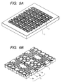
- Figs. 9A and 9B are a perspective view and an enlarged partial view, respectively illustrating the manufacture process for the IC package of the first embodiment.
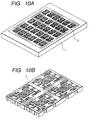
- Figs. 10A and 10B are a perspective view and an enlarged partial view, respectively illustrating the manufacture process for the IC package of the first embodiment.
- Figs. 11 and 12 are enlarged partial views illustrating the manufacture processes for the IC package of the first embodiment.
- Figs. 13A and 13B are a perspective view showing the structure of an IC package and a perspective view of a printed circuit board, according to a second embodiment of the invention.
- Fig. 14 is a vertical cross sectional view of the IC package taken along line 14-14 of Fig. 13A.
- Fig. 15 is a perspective view showing the structure of an IC package according to a third embodiment of the invention.
- Fig. 16 is a vertical cross sectional view of the IC package taken along line 16-16 of Fig. 15.
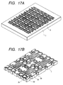
- Figs. 17A and 17B are a perspective view and an enlarged partial view, respectively illustrating the manufacture process for the IC package of the third embodiment.
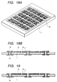
- Figs. 18A and 18B are a perspective view and an enlarged partial view, respectively illustrating the manufacture process for the IC package of the third embodiment.
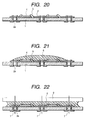
- Figs. 19 to 22 are cross sectional views illustrating the manufacture processes for the IC packages of the third embodiment.
- Fig. 23 is a perspective view of an IC package according to another embodiment of the invention.
- Fig. 24 is a schematic cross sectional view showing a modification of the IC package shown in Fig. 13.
- Figs. 7A and 7B are a perspective view showing the structure of an IC package and a perspective view of a printed circuit board, according to the first embodiment of the invention.
- Fig. 8 is a vertical cross sectional view of the IC package taken along line 8-8 of Fig. 7A.
- reference numeral 1a represents a printed circuit board mounted on which is an IC of a semiconductor memory, a microprocessor, a digital signal processor, a photosensor, a semiconductor laser, an LED, or the like
- reference numeral 2 represents a circuit pattern
- reference numeral 3 represents an insulating film
- reference numeral 4 represents an IC chip
- reference numeral 5 represents a bonding wire
- reference numeral 6 represents a sealing resin.
- the circuit pattern 2 is formed on the printed circuit board 1a and is constituted by a recess portion 2a, a pad portion 2b, an IC chip mount portion 2c, and a wiring portion 2d for connecting these portions.
- the side wall of the recess portion 2a is plated with solderable metal so that an external circuit can be electrically connected to this soldered area which becomes an external connection terminal.
- the material of the printed circuit board 1a may be polyimide, glass epoxy resin, or ceramic.
- recess portions 2a (formed by cutting the printed circuit board along the center lines of through holes disposed in line) are formed at all four sides of the printed circuit board 1a.
- the recess portions 2a may be formed at desired positions depending upon the conditions of connections to external circuits.
- the recess portions 2a may be formed only longer sides of the printed circuit board 1a of a rectangular shape. Through holes not cut may be left in the printed circuit board 1a.
- a printed circuit board 1 is prepared which is formed with a prescribed circuit pattern 2 as shown in Figs. 9A and 9B.
- Figs. 9A and 9B are a perspective view and an enlarged partial view, respectively of the printed circuit board.
- the side wall of each through hole of a cylinder or prism shape formed in the printed circuit board has been plated with solderable metal.
- the circuit pattern 2 is constituted by a through hole portion 2a, a pad portion 2b, an IC chip mount portion 2c, and a wiring portion 2d for connecting these portions.
- the through holes are disposed in a lattice pattern.
- Fig. 10A is a perspective view of the printed circuit board 1
- Fig. 10B is an enlarged partial view thereof (Figs. 11 and 12 show only the enlarged partial views).
- Some unnecessary areas of the insulating film 3 may be cut in advance in a lattice shape so as to expose the areas of the pad portions 2b and IC chip mount portions 2c, or the insulating film 3 may be adhered first over the whole surface and thereafter unnecessary areas are removed. In this embodiment, the unnecessary areas were removed by the processes of mask exposure and development after a photosensitive resist film was adhered.
- IC chips are mounted and connected to the circuit pattern 2 by bonding wires 5 through a wire bonding method or the like.
- liquid sealing resin 6 is coated on the printed circuit board 1 in order to protect the IC chip 4 and bonding wires 5.
- the sealing resin 6 since the openings of the through holes are covered with the insulating film 3, the sealing resin 6 will not enter the through holes 2a and flow to the back surface of the printed circuit board 1. It is therefore unnecessary to determine the coating area by using a mold, mold frame, or the like.
- the sealing resin 6 covers the whole surface of the printed circuit board 1, it may cover only the IC chip 4 and bonding wires 5.
- the printed circuit board 1 is cut along a line on which through holes are aligned.
- the printed circuit board 1 together with the sealing resin 6 is cut along a line 7 shown in Fig. 12 to obtain each lead-less package such as shown in Fig. 7A having recess portions at the side wall and external connection terminals of the conductive members at the recess portions.
- the IC chips mounted on the printed circuit board may be wire bonded prior to covering the openings of through holes with the insulating film.
- an aspect of the present invention resides in that conventional printed circuit board manufacture processes can be used without a use of metal molds for resin sealing and lead frame manufacture.
- a lead-less package of this structure can be soldered to external circuits at the recesses 2a by a usual surface mount method (reflow soldering or the like), so that mount is easy and cost effective.
- sealing resin is light transmissive epoxy resin such as NT-8000 (product name) manufactured by Nitto Electric Industry Co. Ltd, and if IC chips of photoactive elements are used such as a photosensor, a light emitting diode, then semiconductor optical devices can be manufactured without using metal molds.
- a plurality of through holes in a printed circuit board can be used as external connection terminals. Therefore, metal molds for lead frames and resin sealing are not required to be prepared for each type of IC chips as in conventional cases. Accordingly, immense investment in facilities is not necessary even for production of a small number of products of a variety of product types, and even for mass production with low assembly cost.
- Figs. 13A and 13B are a perspective view showing the structure of an IC package and a perspective view of a printed circuit board, according to the second embodiment of the invention.
- Fig. 14 is a vertical cross sectional view of the IC package taken along line 14-14 of Fig. 13A.
- reference numeral 1a represents a printed circuit board mounted on which is an IC of a semiconductor memory, a microprocessor, a digital signal processor, a photosensor, a semiconductor laser, an LED, or the like
- reference numeral 2 represents a circuit pattern
- reference numeral 3 represents an insulating film
- reference numeral 4 represents an IC chip
- reference numeral 5 represents a bonding wire
- reference numeral 6 represents a sealing resin
- reference numeral 9 represents a light permissive member.
- the circuit pattern 2 is formed on the printed circuit board 1a and is constituted by a recess portion (through hole portion) 2a, a pad portion 2b, an IC chip mount portion 2c, and a wiring portion 2d for connecting these portions.
- the side wall of the recess portion 2a is plated with solderable metal so that an external circuit can be electrically connected to this soldered area which becomes an external connection terminal.
- the recess portions are formed by cutting the printed circuit board along the center lines of through holes disposed in line.
- Fig. 15 is a perspective view showing the structure of an IC package according to the third embodiment of the invention.
- Fig. 16 is a vertical cross sectional view of the IC package taken along line 16-16 of Fig. 15.
- reference numeral 1a represents a printed circuit board mounted on which is an IC of a semiconductor memory, a microprocessor, a digital signal processor, a photosensor, a semiconductor laser, an LED, or the like
- reference numeral 2 represents a circuit pattern
- reference numeral 3 represents an insulating film
- reference numeral 4 represents an IC chip
- reference numeral 5 represents a bonding wire
- reference numeral 6 represents a sealing resin
- reference numeral 9 represents a light permissive member.
- the circuit pattern 2 is formed on the printed circuit board 1a and is constituted by a through hole portion 2a, a pad portion 2b, an IC chip mount portion 2c, and a wiring portion 2d for connecting these portions.
- the through hole portion 2a is filled with conductive material 3a so that an external circuit can be electrically connected to this conducive material by soldering, the conductive material becoming an external connection terminal.
- the material of the printed circuit board 1a may be polyimide, glass epoxy resin, or ceramic.
- through hole portions 2a are formed at all four sides of the printed circuit board 1a.
- the through hole portions 2a may be formed at desired positions depending upon the conditions of connections to external circuits.
- the through hole portions 2a may be formed only longer sides of the printed circuit board 1a of a rectangular shape. Through holes not cut may be left in the printed circuit board 1a.
- IC package The manufacture method of the IC package will be described with reference to Fig. 17A to Fig. 22.
- an IC of a photosensor as a semiconductor optical element is used by way of example.
- a printed circuit board 1 is prepared which is formed with a prescribed circuit pattern 2 as shown in Figs. 17A and 17B.
- Figs. 17A and 17B are a perspective view and an enlarged partial view, respectively of the printed circuit board.
- the side wall of each through hole formed in the printed circuit board has been plated with solderable metal.
- the circuit pattern 2 is constituted by a through hole portion 2a, a pad portion 2b, an IC chip mount portion 2c, and a wiring portion 2d for connecting these portions.
- Fig. 18A is a perspective view of the printed circuit board covered with the insulating films
- Fig. 18B is an enlarge partial view in section of the printed circuit board
- Fig. 19 is an enlarged partial view in section of the printed circuit board with through holes being filled with conductive material (Figs. 20 to 22 show only the enlarged partial views in section).
- the through holes are filled with the conductive material 3a after plating, they may be filled by the same single process.
- some unnecessary areas of the insulating film 3b may be cut in advance (for example, in a lattice shape) or it may be adhered first over the whole surface and thereafter unnecessary areas are removed. In this embodiment, the unnecessary areas were removed by the processes of mask exposure and development after a photosensitive resist film was adhered.
- the printed circuit board with through holes being filled with the conductive material 3a is omitted, and only the printed circuit using the insulating film 3b is shown. The same processes are executed for both types of the printed circuit boards.
- IC chips are mounted and connected to the circuit or lead pattern 2 by bonding wires 5 through a wire bonding method or the like.
- liquid sealing resin 6 is coated on the printed circuit board 1 in order to protect the IC chip 4 and bonding wires 5.
- the sealing resin 6 since the openings of the through holes are filled with the conductive material 3a (not shown) or covered with the insulating film 3, the sealing resin 6 will not enter the through holes 2a and flow to the back surface of the printed circuit board 1. It is therefore unnecessary to determine the coating area by using a mold, mold frame, or the like.
- the light permissive member 9 is placed on the transparent resin 6 in parallel to the printed circuit board 1 to make the gap between the printed circuit board 1 and light transmissive member 9 be filled with the transparent resin 6.
- the printed circuit board 1 is cut along a line on which through holes are aligned.
- the printed circuit board 1 together with the sealing resin 6 and light transmissive member 9 is cut along a line 7 such as shown in Fig. 22 to obtain each lead-less package such as shown in Figs. 13A to 14 of the second embodiment and each lead-less package such as shown in Fig. 16 of the third embodiment.
- the IC chips mounted on the printed circuit board may be wire bonded prior to filling in the openings of the through holes.
- an aspect of the present invention resides in that conventional printed circuit board manufacture processes can be used without a use of metal molds for resin sealing and lead frame manufacture.
- a lead-less package of this structure can be soldered to external circuits by a usual surface mount method (reflow soldering or the like), so that mount is easy and cost effective.
- BT resin product name
- a photosensitive resist film was used for the insulating film 3b
- World Lock No. 801 SE-L and XVL-01L product names manufactured by Kyoritsu Chemical Industry Co. Ltd. were used as the transparent resin 6
- a phosphosilicate glass plate was uses as the light transmissive member 9.
- IC packages excellent in heat resistance of solder and optical performance were able to be manufactured.
- CM-5000 product name
- HOYA CORP HOYA CORP
- the spectral sensitivity of the photosensor can be adjusted to from the photosensor with desired characteristics. If a specific color is to be cut, colored resin or light permissive member may be used. In the case of an IC not using light, non-light transmissive resin or other materials may be used.
- Fig. 23 is a perspective view of an IC package according to another embodiment of the invention.
- Recesses 2a to be used as external connection terminals are provided at the four sides of a printed circuit board 1a.
- An IC chip 4 is disposed on a chip mount portion 2c at the upper surface of the board 1a.
- Bonding pads of the IC chip 4 and bonding pad areas of a wiring patter are electrically connected by bonding wires 5.
- the length of the wiring pattern 2d is made longer so that corrosion can be avoided which is otherwise caused by water contents entered from the edges of the IC package.
- the wiring pattern 2d is deflected at several points as shown in Fig. 23.
- Reference numeral 3b represents an insulting film
- reference numeral 6 represents resin
- reference numeral 9 represents a protective member
- an optical active element is used as the IC chip 4
- transparent resin was selected as the resin 6
- a light permissive rigid member was selected as the member 9.
- the thickness (length) from the package surface to the light receiving portion (or light emitting portion) is relatively thick in order to adversely affected by reflected light (Japanese Patent Laid-open Application No. 63-21878).
- the member 9 is adhered to make the thickness between the surface of the member 9 to the light receiving portion 4a thicker.
- This IC package can by manufactured by the method illustrated with reference to Figs. 17A to 22.
- a member may be adhered to the package resin 6, the member 9 may be adhered after each package is cut after curing of the resin, or may be adhered to each cured resin and thereafter each package is cut. Since these methods may lower throughput. Therefore, as described with Figs. 17A to 22, preferably, after the member 9 is disposed, the resin is cured and then the member 9, cured resin 6, and the printed circuit board 1 are cut at the same time.
- a plurality of through holes in a printed circuit board can be used as external connection terminals. Therefore, metal molds for lead frames and resin sealing are not required to be prepared for each type of IC chips as in conventional cases. Accordingly, immense investment in facilities is not necessary even for production of a small number of products of a variety of product types, and even for mass production with low assembly cost.
- the outer dimension of the IC package can be made very small.
- An IC package has a substrate having recesses formed on the side wall thereof, an insulating film for covering an opening of each recess on the side of a principal surface of the substrate, and an IC chip mounted on a mount surface side of the film on the substrate, wherein a conductive portion formed on each recess is used as an external connection terminal for the IC chip.
- a method of assembling an IC package has the steps of forming a substrate having a plurality of through holes each having an insulating film covering one of the openings of each through hole, mounting one or more IC chips on a principal surface of the substrate on the insulating film side, and electrically connecting the IC chip and the through holes, sealing the substrate with the IC chip mounted thereon with insulating resin, and cut the substrate with the IC chip mounted thereon to expose the side wall of each through hole.
Abstract
Description
- The present invention relates to a package for integrated circuits and its assembly method.
- In order to assemble an IC chip on a circuit board, the IC chip is first assembled in a resin sealed package using a lead frame such as those shown in Figs. 1 to 5 or in a package with a hollow portion such as shown in Fig. 6.
- The assembly method for resin sealed packages shown in Figs. 1 to 5 will be described.
- First, photosensor IC chips are placed on a lead frame (shown in Fig. 1) made of a thin metal plate on which a predetermined circuit pattern is formed through pressing or etching, connections are made by using bonding wires 5 (shown in Fig. 2), and the photosensor IC chips are molded with transparent thermosetting resin 6 (shown in Fig. 3). Thereafter, leads are cut and shaped into a predetermined configuration (shown in Fig. 4). This method is widely adopted because mass production is possible and soldering to a circuit board is relatively easy.
- In order to package an IC having a photosensor element, a light
transmissive member 9 such as shown in Fig. 5 is bonded in order to prevent damages on a light incidence plane and eliminate unnecessary light reflection (Japanese Patent Laid-open Application No. 63-21878). - For assembly of the package shown in Fig. 6, a
photosensor IC chip 4 is placed in ahollow portion 10 of a ceramic or resin mold, connections are made by using bonding wires, and thehollow portion 10 is covered with a lightpermissive member 9 to hermetically seal it. With this structure, a bonding margin for maintaining the hermetic seal must be prepared, resulting in a large package size. - These conventional methods are associated with various issues to be solved. For example, expensive metal molds are required to be prepared for each type of a package. Production of various types of packages requires immense investment in facilities. It takes a long time to complete a sample which requires new metal molds. Leads are likely to be broken depending upon how the package is dealt with. An additional process for bonding the light
permissive member 9 is required and the assembly cost rises. - A package of a lead-less structure has been proposed using a both-side printed circuit board in place of a lead frame (Japanese Patent Laid-open Application No. 2-2150). However, this method uses metal molds like the above methods so that it is associated with similar problems.
- It is an object of the present invention to provide an IC package and its assembly method capable of dispensing with metal molds, unnecessary for immense investment in facilities even for production of various types of packages, applicable to mass production with low assembly cost, and easy to solder an IC chip to a circuit board.
- It is another object of the present invention to solve the above problems and provide an IC package comprising: a substrate having recesses formed on the side wall thereof; an insulating film for covering an opening of each recess on the side of a principal surface of the substrate; and an IC chip mounted on a mount surface side of the film on the substrate, wherein a conductive portion formed on each recess is used as an external connection terminal for the IC chip.
- It is an object of the present invention to provide a method of assembling an IC package comprising the steps of: forming a substrate having a plurality of through holes each having an insulating film covering one of the openings of each through hole; mounting one or more IC chips on a principal surface of the substrate on the insulating film side, and electrically connecting the IC chip and the through holes; sealing the substrate with the IC chip mounted thereon with insulating resin; and cut the substrate with the IC chip mounted thereon to expose the side wall of each through hole.
- It is another object of the present invention to provid an IC package comprising: a substrate having recesses formed on the side wall thereof; an insulating film for covering an opening of each recess on the side of a principal surface of the substrate; an IC chip mounted on a mount surface side of the film on the substrate; a resin portion for sealing the IC chip; and a rigid member formed on the resin portion, wherein a conductive portion formed on each recess is used as an external connection terminal for the IC chip.
- It is another object of the present invention to provide an IC package comprising: a substrate having recesses on the side wall thereof, the recesses being filled with conductive material; an IC chip mounted on one principal surface of the substrate; a transparent resin portion for sealing the IC chip; and a light transmissive member formed on the transparent region portion, wherein the filled conductive material at the side wall of the substrate is used as an external connection terminal for said photosensor IC chip.
- It is another object of the present invention to provide a method of assembling an IC package comprising the steps of: forming a substrate having a plurality of through holes each having an insulating film covering one of the openings of each through hole; mounting one or more IC chips on a principal surface of the substrate on the insulating film side, and electrically connecting the IC chip and the through holes; forming a light transmissive member on a transparent resin portion formed on the substrate having the IC chip mounted thereon; and cut the substrate with the IC chip mounted thereon to expose the side wall of each through hole.
- It is another object of the present invention to provide a method of assembling an IC package comprising the steps of: forming a substrate having a plurality of through holes each having conductive material filled in the opening of each through hole; mounting one or more IC chips on a principal surface of the substrate on the insulating film side, and electrically connecting the IC chip and the through holes; forming a light transmissive member on a transparent resin portion formed on the substrate having the IC chip mounted thereon; and cut the substrate with the IC chip mounted thereon to expose the conductive material in each through hole.
- According to the invention, a plurality of through holes in a printed circuit board are used as external connection terminals, instead of using conventional leads. Therefore, metal molds for lead frames are not required to be prepared for each type of IC chips as in conventional cases.
- Since the through hole is covered with an insulating film or filled with conductive material, resin will not flow via the through hole to the back surface of the substrate, it is not necessary to prepare metal molds for stopping a flow of resin.
- Since the side wall of the through hole cut vertically or the conductive material in the cut through hole are used as an external connection terminal, leads are broken lesser than conventional leads.
- If transparent resin is used when necessary and a light transmissive member having a high rigidity such as glass is placed on the transparent resin, it becomes possible to prevent damages on the surface of the transparent resin and becomes easy to retain optical flatness. An IC package of this invention is preferably used for optical semiconductor elements such as optical sensors, light emitting diodes, and semiconductor lasers.
- Since the light permissive member is adhered at the same time when the resin is coated and cured, an increase in the number of processes can be prevented. Furthermore, since an additional margin is not necessary, the outer dimension of the IC package can be made small.
- Figs. 1 to 4 are plan views illustrating assembly processes according to conventional techniques.
- Fig. 5 is a cross sectional view illustrating an assembly process according to a conventional technique.
- Fig. 6 is a cross sectional view of a package according to a conventional technique.
- Figs. 7A and 7B are a perspective view showing the structure of an IC package and a perspective view of a printed circuit board, according to a first embodiment of the invention.
- Fig. 8 is a vertical cross sectional view of the IC package taken along line 8-8 of Fig. 7A.
- Figs. 9A and 9B are a perspective view and an enlarged partial view, respectively illustrating the manufacture process for the IC package of the first embodiment.
- Figs. 10A and 10B are a perspective view and an enlarged partial view, respectively illustrating the manufacture process for the IC package of the first embodiment.
- Figs. 11 and 12 are enlarged partial views illustrating the manufacture processes for the IC package of the first embodiment.
- Figs. 13A and 13B are a perspective view showing the structure of an IC package and a perspective view of a printed circuit board, according to a second embodiment of the invention.
- Fig. 14 is a vertical cross sectional view of the IC package taken along line 14-14 of Fig. 13A.
- Fig. 15 is a perspective view showing the structure of an IC package according to a third embodiment of the invention.
- Fig. 16 is a vertical cross sectional view of the IC package taken along line 16-16 of Fig. 15.
- Figs. 17A and 17B are a perspective view and an enlarged partial view, respectively illustrating the manufacture process for the IC package of the third embodiment.
- Figs. 18A and 18B are a perspective view and an enlarged partial view, respectively illustrating the manufacture process for the IC package of the third embodiment.
- Figs. 19 to 22 are cross sectional views illustrating the manufacture processes for the IC packages of the third embodiment.
- Fig. 23 is a perspective view of an IC package according to another embodiment of the invention.
- Fig. 24 is a schematic cross sectional view showing a modification of the IC package shown in Fig. 13.
- Embodiments of the present invention will be described in detail with reference to the accompanying drawings.
- Figs. 7A and 7B are a perspective view showing the structure of an IC package and a perspective view of a printed circuit board, according to the first embodiment of the invention. Fig. 8 is a vertical cross sectional view of the IC package taken along line 8-8 of Fig. 7A.
- In Figs. 7A and 7B and Fig. 8,
reference numeral 1a represents a printed circuit board mounted on which is an IC of a semiconductor memory, a microprocessor, a digital signal processor, a photosensor, a semiconductor laser, an LED, or the like,reference numeral 2 represents a circuit pattern,reference numeral 3 represents an insulating film,reference numeral 4 represents an IC chip,reference numeral 5 represents a bonding wire, andreference numeral 6 represents a sealing resin. Thecircuit pattern 2 is formed on the printedcircuit board 1a and is constituted by arecess portion 2a, apad portion 2b, an ICchip mount portion 2c, and awiring portion 2d for connecting these portions. The side wall of therecess portion 2a is plated with solderable metal so that an external circuit can be electrically connected to this soldered area which becomes an external connection terminal. The material of the printedcircuit board 1a may be polyimide, glass epoxy resin, or ceramic. In this example,recess portions 2a (formed by cutting the printed circuit board along the center lines of through holes disposed in line) are formed at all four sides of the printedcircuit board 1a. Therecess portions 2a may be formed at desired positions depending upon the conditions of connections to external circuits. For example, therecess portions 2a may be formed only longer sides of the printedcircuit board 1a of a rectangular shape. Through holes not cut may be left in the printedcircuit board 1a. - The manufacture method of the IC package will be described with reference to Figs. 9A and 9B to Fig. 12.
- First, a printed
circuit board 1 is prepared which is formed with aprescribed circuit pattern 2 as shown in Figs. 9A and 9B. Figs. 9A and 9B are a perspective view and an enlarged partial view, respectively of the printed circuit board. The side wall of each through hole of a cylinder or prism shape formed in the printed circuit board has been plated with solderable metal. Thecircuit pattern 2 is constituted by a throughhole portion 2a, apad portion 2b, an ICchip mount portion 2c, and awiring portion 2d for connecting these portions. The through holes are disposed in a lattice pattern. - Next, as shown in Figs. 10A and 10B, an insulating
film 3 is adhered covering the openings of all through holes in the printedcircuit board 1. Fig. 10A is a perspective view of the printedcircuit board 1, and Fig. 10B is an enlarged partial view thereof (Figs. 11 and 12 show only the enlarged partial views). Some unnecessary areas of the insulatingfilm 3 may be cut in advance in a lattice shape so as to expose the areas of thepad portions 2b and ICchip mount portions 2c, or the insulatingfilm 3 may be adhered first over the whole surface and thereafter unnecessary areas are removed. In this embodiment, the unnecessary areas were removed by the processes of mask exposure and development after a photosensitive resist film was adhered. - Thereafter, as shown in Fig. 11, IC chips are mounted and connected to the
circuit pattern 2 bybonding wires 5 through a wire bonding method or the like. - Next, as shown in Fig. 12,
liquid sealing resin 6 is coated on the printedcircuit board 1 in order to protect theIC chip 4 andbonding wires 5. In this case, since the openings of the through holes are covered with the insulatingfilm 3, the sealingresin 6 will not enter the throughholes 2a and flow to the back surface of the printedcircuit board 1. It is therefore unnecessary to determine the coating area by using a mold, mold frame, or the like. In this embodiment, although the sealingresin 6 covers the whole surface of the printedcircuit board 1, it may cover only theIC chip 4 andbonding wires 5. - After the sealing
resin 6 is cured through placement in environmental atmosphere, heating, ultraviolet radiation, or the like, the printedcircuit board 1 is cut along a line on which through holes are aligned. In this embodiment, the printedcircuit board 1 together with the sealingresin 6 is cut along aline 7 shown in Fig. 12 to obtain each lead-less package such as shown in Fig. 7A having recess portions at the side wall and external connection terminals of the conductive members at the recess portions. In the IC package manufacture method of this embodiment, the IC chips mounted on the printed circuit board may be wire bonded prior to covering the openings of through holes with the insulating film. - As apparent from the above description, an aspect of the present invention resides in that conventional printed circuit board manufacture processes can be used without a use of metal molds for resin sealing and lead frame manufacture.
- A lead-less package of this structure can be soldered to external circuits at the
recesses 2a by a usual surface mount method (reflow soldering or the like), so that mount is easy and cost effective. - If sealing resin is light transmissive epoxy resin such as NT-8000 (product name) manufactured by Nitto Electric Industry Co. Ltd, and if IC chips of photoactive elements are used such as a photosensor, a light emitting diode, then semiconductor optical devices can be manufactured without using metal molds.
- As described so far, according to the first embodiment, a plurality of through holes in a printed circuit board can be used as external connection terminals. Therefore, metal molds for lead frames and resin sealing are not required to be prepared for each type of IC chips as in conventional cases. Accordingly, immense investment in facilities is not necessary even for production of a small number of products of a variety of product types, and even for mass production with low assembly cost.
- Since the side walls of the recesses exposed by cutting the printed circuit board along a line of aligned through holes are used as the external connection terminals, the mechanical structure is robust and there is less possibility of breakage.
- Next, the second embodiment of the present invention will be described in detail with reference to the accompanying drawing.
- Figs. 13A and 13B are a perspective view showing the structure of an IC package and a perspective view of a printed circuit board, according to the second embodiment of the invention. Fig. 14 is a vertical cross sectional view of the IC package taken along line 14-14 of Fig. 13A.
- In Figs. 13A and 13B and Fig. 14,
reference numeral 1a represents a printed circuit board mounted on which is an IC of a semiconductor memory, a microprocessor, a digital signal processor, a photosensor, a semiconductor laser, an LED, or the like,reference numeral 2 represents a circuit pattern,reference numeral 3 represents an insulating film,reference numeral 4 represents an IC chip,reference numeral 5 represents a bonding wire,reference numeral 6 represents a sealing resin, andreference numeral 9 represents a light permissive member. Thecircuit pattern 2 is formed on the printedcircuit board 1a and is constituted by a recess portion (through hole portion) 2a, apad portion 2b, an ICchip mount portion 2c, and awiring portion 2d for connecting these portions. The side wall of therecess portion 2a is plated with solderable metal so that an external circuit can be electrically connected to this soldered area which becomes an external connection terminal. The recess portions are formed by cutting the printed circuit board along the center lines of through holes disposed in line. - Fig. 15 is a perspective view showing the structure of an IC package according to the third embodiment of the invention. Fig. 16 is a vertical cross sectional view of the IC package taken along line 16-16 of Fig. 15.
- In Figs. 15 and 16,
reference numeral 1a represents a printed circuit board mounted on which is an IC of a semiconductor memory, a microprocessor, a digital signal processor, a photosensor, a semiconductor laser, an LED, or the like,reference numeral 2 represents a circuit pattern,reference numeral 3 represents an insulating film,reference numeral 4 represents an IC chip,reference numeral 5 represents a bonding wire,reference numeral 6 represents a sealing resin, andreference numeral 9 represents a light permissive member. Thecircuit pattern 2 is formed on the printedcircuit board 1a and is constituted by a throughhole portion 2a, apad portion 2b, an ICchip mount portion 2c, and awiring portion 2d for connecting these portions. The throughhole portion 2a is filled withconductive material 3a so that an external circuit can be electrically connected to this conducive material by soldering, the conductive material becoming an external connection terminal. - The material of the printed
circuit board 1a may be polyimide, glass epoxy resin, or ceramic. In the second and third embodiments, throughhole portions 2a are formed at all four sides of the printedcircuit board 1a. The throughhole portions 2a may be formed at desired positions depending upon the conditions of connections to external circuits. For example, the throughhole portions 2a may be formed only longer sides of the printedcircuit board 1a of a rectangular shape. Through holes not cut may be left in the printedcircuit board 1a. - The manufacture method of the IC package will be described with reference to Fig. 17A to Fig. 22. In this method, an IC of a photosensor as a semiconductor optical element is used by way of example.
- First, a printed
circuit board 1 is prepared which is formed with aprescribed circuit pattern 2 as shown in Figs. 17A and 17B. Figs. 17A and 17B are a perspective view and an enlarged partial view, respectively of the printed circuit board. The side wall of each through hole formed in the printed circuit board has been plated with solderable metal. Thecircuit pattern 2 is constituted by a throughhole portion 2a, apad portion 2b, an ICchip mount portion 2c, and awiring portion 2d for connecting these portions. - Next, all the through holes in the printed
circuit board 1 are filled withconductive material 3a as shown in Fig. 19, or covered with an insulatingfilm 3b. Fig. 18A is a perspective view of the printed circuit board covered with the insulating films, and Fig. 18B is an enlarge partial view in section of the printed circuit board. Fig. 19 is an enlarged partial view in section of the printed circuit board with through holes being filled with conductive material (Figs. 20 to 22 show only the enlarged partial views in section). Although the through holes are filled with theconductive material 3a after plating, they may be filled by the same single process. In covering the through holes with the insulatingfilm 3b, some unnecessary areas of the insulatingfilm 3b may be cut in advance (for example, in a lattice shape) or it may be adhered first over the whole surface and thereafter unnecessary areas are removed. In this embodiment, the unnecessary areas were removed by the processes of mask exposure and development after a photosensitive resist film was adhered. In Figs. 20 to 22, for the drawing simplicity, the printed circuit board with through holes being filled with theconductive material 3a is omitted, and only the printed circuit using the insulatingfilm 3b is shown. The same processes are executed for both types of the printed circuit boards. - Thereafter, as shown in Fig. 20, IC chips are mounted and connected to the circuit or
lead pattern 2 bybonding wires 5 through a wire bonding method or the like. - Next, as shown in Fig. 21,
liquid sealing resin 6 is coated on the printedcircuit board 1 in order to protect theIC chip 4 andbonding wires 5. In this case, since the openings of the through holes are filled with theconductive material 3a (not shown) or covered with the insulatingfilm 3, the sealingresin 6 will not enter the throughholes 2a and flow to the back surface of the printedcircuit board 1. It is therefore unnecessary to determine the coating area by using a mold, mold frame, or the like. - As shown in Fig. 22, prior to curing of the
transparent resin 6, the lightpermissive member 9 is placed on thetransparent resin 6 in parallel to the printedcircuit board 1 to make the gap between the printedcircuit board 1 andlight transmissive member 9 be filled with thetransparent resin 6. - After the
transparent resin 6 is cured through placement in environmental atmosphere, heating, ultraviolet radiation, or the like while the gap between the printedcircuit board 1 andlight transmissive member 9 is maintained constant by using a jig (not shown) or the like, the printedcircuit board 1 is cut along a line on which through holes are aligned. In these embodiments, the printedcircuit board 1 together with the sealingresin 6 andlight transmissive member 9 is cut along aline 7 such as shown in Fig. 22 to obtain each lead-less package such as shown in Figs. 13A to 14 of the second embodiment and each lead-less package such as shown in Fig. 16 of the third embodiment. In the photosensor IC package manufacture method of this embodiment, the IC chips mounted on the printed circuit board may be wire bonded prior to filling in the openings of the through holes. - As apparent from the above description, an aspect of the present invention resides in that conventional printed circuit board manufacture processes can be used without a use of metal molds for resin sealing and lead frame manufacture.
- A lead-less package of this structure can be soldered to external circuits by a usual surface mount method (reflow soldering or the like), so that mount is easy and cost effective.
- In the above embodiments, BT resin (product name) manufactured by Mitsubishi Gas Chemical Co. Ltd was used for the printed
circuit board 1, a photosensitive resist film was used for the insulatingfilm 3b, World Lock No. 801 SE-L and XVL-01L (product names) manufactured by Kyoritsu Chemical Industry Co. Ltd. were used as thetransparent resin 6, and a phosphosilicate glass plate was uses as thelight transmissive member 9. IC packages excellent in heat resistance of solder and optical performance were able to be manufactured. - If an infrared cut filter made of CM-5000 (product name) manufactured by HOYA CORP. is used in place of the
light transmissive member 9, the spectral sensitivity of the photosensor can be adjusted to from the photosensor with desired characteristics. If a specific color is to be cut, colored resin or light permissive member may be used. In the case of an IC not using light, non-light transmissive resin or other materials may be used. - Fig. 23 is a perspective view of an IC package according to another embodiment of the invention.
-
Recesses 2a to be used as external connection terminals are provided at the four sides of a printedcircuit board 1a. AnIC chip 4 is disposed on achip mount portion 2c at the upper surface of theboard 1a. - Bonding pads of the
IC chip 4 and bonding pad areas of a wiring patter are electrically connected bybonding wires 5. - The length of the
wiring pattern 2d is made longer so that corrosion can be avoided which is otherwise caused by water contents entered from the edges of the IC package. In order to dispose a longer wiring pattern in a narrow space, thewiring pattern 2d is deflected at several points as shown in Fig. 23. - Water contents immerse into the package along a conductive wiring pattern. Therefore, if the effective length from the
external connection terminal 2a to thebonding pad area 2b is elongated, durability of the IC package can be improved. -
Reference numeral 3b represents an insulting film,reference numeral 6 represents resin, andreference numeral 9 represents a protective member. - In this embodiment, an optical active element is used as the
IC chip 4, transparent resin was selected as theresin 6, and a light permissive rigid member was selected as themember 9. - For the IC package, particularly an IC package using an optical active element, it is necessary for the thickness (length) from the package surface to the light receiving portion (or light emitting portion) to be relatively thick in order to adversely affected by reflected light (Japanese Patent Laid-open Application No. 63-21878). In this embodiment, the
member 9 is adhered to make the thickness between the surface of themember 9 to thelight receiving portion 4a thicker. - This IC package can by manufactured by the method illustrated with reference to Figs. 17A to 22.
- If an IC chip with an optical semiconductor device is used, a member may be adhered to the
package resin 6, themember 9 may be adhered after each package is cut after curing of the resin, or may be adhered to each cured resin and thereafter each package is cut. Since these methods may lower throughput. Therefore, as described with Figs. 17A to 22, preferably, after themember 9 is disposed, the resin is cured and then themember 9, curedresin 6, and the printedcircuit board 1 are cut at the same time. - As described so far, according to the invention, a plurality of through holes in a printed circuit board can be used as external connection terminals. Therefore, metal molds for lead frames and resin sealing are not required to be prepared for each type of IC chips as in conventional cases. Accordingly, immense investment in facilities is not necessary even for production of a small number of products of a variety of product types, and even for mass production with low assembly cost.
- Since the soldering margin for the light transmissive member is not necessary, the outer dimension of the IC package can be made very small.
- Since the side walls of the recesses exposed by cutting the printed circuit board along a line of aligned through holes are used as the external connection terminals, the mechanical structure is robust and there is less possibility of breakage.
- An IC package has a substrate having recesses formed on the side wall thereof, an insulating film for covering an opening of each recess on the side of a principal surface of the substrate, and an IC chip mounted on a mount surface side of the film on the substrate, wherein a conductive portion formed on each recess is used as an external connection terminal for the IC chip. A method of assembling an IC package has the steps of forming a substrate having a plurality of through holes each having an insulating film covering one of the openings of each through hole, mounting one or more IC chips on a principal surface of the substrate on the insulating film side, and electrically connecting the IC chip and the through holes, sealing the substrate with the IC chip mounted thereon with insulating resin, and cut the substrate with the IC chip mounted thereon to expose the side wall of each through hole.
Claims (24)
- An IC package comprising:a substrate having recesses formed on the side wall thereof;an insulating film for covering an opening of each said recess on the side of a principal surface of said substrate; andan IC chip mounted on a mount surface side of said film on said substrate,wherein a conductive portion formed on each said recess is used as an external connection terminal for said IC chip.
- An IC package according to claim 1, wherein the whole principal surface of said IC chip on the IC chip mount side is sealed with insulating resin.
- An IC package according to claim 1, wherein said insulating film covers only the opening and its peripheral area.
- An IC package according to claim 1, wherein said substrate has a circuit pattern including a pad portion for electrical connection to said IC chip, an IC chip mount portion, and a wiring portion for connection of said pad portion and said IC chip mount portion to the conductive portion.
- A method of assembling an IC package comprising the steps of:forming a substrate having a plurality of through holes each having an insulating film covering one of the openings of each through hole;mounting one or more IC chips on a principal surface of the substrate on the insulating film side, and electrically connecting the IC chip and the through holes;sealing the substrate with the IC chip mounted thereon with insulating resin; andcut the substrate with the IC chip mounted thereon to expose the side wall of each through hole.
- A method according to claim 5, wherein said step of electrically connecting the IC chip to the through holes performs wire bonding between the IC chip and pad portions connected to the through holes.
- A method according to claim 5, wherein the IC chip has an optical active element and the insulating resin is light permissive resin.
- A method according to claim 5, wherein the plurality of through holes are disposed in a lattice shape.
- An IC package comprising:a substrate having a concave side;an insulating film sealing an opening at the concave side of said substrate;IC chip mounted on a side of said substrate, on which said film is arranged;a resin sealing said IC chip; anda rigid member provided on said resin;wherein a conductive section formed in the concave side is used as an external connection terminal of the IC chip.
- An IC package comprising:a substrate having, at a side, a cut through hole filled with a conductive material;a photosensor IC chip mounted on one major surface of said substrate;a transparent resin sealing said photosensor IC chip; anda right transmitting member provided on said transparent resin,wherein the conductive member at the side of said substrate is used as an external connection terminal of said photosensor IC chip.
- A method for producing a photosensor IC package comprising steps of:forming a substrate having a through holes of which openings at one side are sealed with an insulating film;mounting one or more the photosensor IC chips on a major surface of the substrate, on which the film is arranged;providing a light transmitting member through a transparent resin on the substrate on which the photosensor IC chip is mounted; andcutting the substrate on which the photosensor IC chip is mounted, so that a wall of the through holes are exposed.
- A method for producing a photosensor IC chip comprising steps of:forming a substrate having plural through holes of which openings are filled with a conductive material;mounting on one major surface of the substrate, one or more photosensor IC chips, and connecting electrically the photosensor IC chips with the through holes;providing on the substrate on which the photosensor IC chip is mounted, a light transmitting member through a transparent resin; andcutting the substrate on which the photosensor IC chip is mounted, so that the conductive material in the through hole is exposed.
- A method according to claim 11 or 12, wherein the plurality of through holes are disposed in a lattice shape.
- An IC package according to claim 1, wherein said recess has a curved surface.
- An IC package according to claim 1, wherein said recess is of a cut cylinder shape.
- An IC package according to claim 1, wherein said recess is of a cut prism shape.
- An IC package according to claim 1, wherein said recess is a cut through hole.
- An IC package according to claim 1, wherein a rigid member is disposed on said insulating resin.
- An IC package according to claim 1, wherein said IC chip is an optical active element, and said insulating resin is transparent and has a light transmissive member formed on the surface thereof.
- An IC package according to claim 1, wherein the surface of said insulating resin is mounted with a light transmissive member having generally the same area as that of said substrate.
- A method according to claim 5, wherein the IC chip is an optical semiconductor element, the insulating resin is transparent resin, and the method further comprising the step of forming a light transmissive member on the insulating resin.
- A method according to claim 5, further comprising the step of forming a rigid member on the cured insulating resin.
- A method according to claim 5, wherein after a rigid member is disposed on the insulating resin, the insulating resin is cured and the substrate is cut.
- A method according to claim 5, wherein after a rigid member is disposed on the insulating resin, the substrate as well as the insulating resin is cut.
Applications Claiming Priority (6)
| Application Number | Priority Date | Filing Date | Title |
|---|---|---|---|
| JP225296/95 | 1995-09-01 | ||
| JP22529795 | 1995-09-01 | ||
| JP22529695 | 1995-09-01 | ||
| JP225297/95 | 1995-09-01 | ||
| JP228079/96 | 1996-08-29 | ||
| JP22807996A JP3507251B2 (en) | 1995-09-01 | 1996-08-29 | Optical sensor IC package and method of assembling the same |
Publications (3)
| Publication Number | Publication Date |
|---|---|
| EP0790653A2 true EP0790653A2 (en) | 1997-08-20 |
| EP0790653A3 EP0790653A3 (en) | 1998-04-15 |
| EP0790653B1 EP0790653B1 (en) | 2006-07-12 |
Family
ID=27331024
Family Applications (1)
| Application Number | Title | Priority Date | Filing Date |
|---|---|---|---|
| EP96113927A Expired - Lifetime EP0790653B1 (en) | 1995-09-01 | 1996-08-30 | IC package and its assembly method |
Country Status (4)
| Country | Link |
|---|---|
| US (1) | US6383835B1 (en) |
| EP (1) | EP0790653B1 (en) |
| JP (1) | JP3507251B2 (en) |
| DE (1) | DE69636335T2 (en) |
Cited By (8)
| Publication number | Priority date | Publication date | Assignee | Title |
|---|---|---|---|---|
| EP1051746A1 (en) * | 1998-02-06 | 2000-11-15 | Shellcase Ltd. | Integrated circuit device |
| US6451628B1 (en) * | 1997-12-25 | 2002-09-17 | Sanyo Electric Co., Ltd. | Method fabricating a semiconductor device with a decreased mounting area |
| EP1317000A2 (en) | 2001-11-30 | 2003-06-04 | Kabushiki Kaisha Toshiba | Semiconductor device having leadless package structure |
| US7335951B2 (en) | 2003-10-06 | 2008-02-26 | Semiconductor Energy Laboratory Co., Ltd. | Semiconductor device and method for manufacturing the same |
| US7408249B2 (en) | 1998-02-06 | 2008-08-05 | Tessera Technologies Hungary Kft. | Packaged integrated circuits and methods of producing thereof |
| US7566853B2 (en) | 2005-08-12 | 2009-07-28 | Tessera, Inc. | Image sensor employing a plurality of photodetector arrays and/or rear-illuminated architecture |
| US8207589B2 (en) | 2007-02-15 | 2012-06-26 | Semiconductor Energy Laboratory Co., Ltd. | Photoelectric conversion device and electronic device, and method for manufacturing photoelectric conversion device |
| EP3787023A4 (en) * | 2018-04-27 | 2022-03-09 | Canon Kabushiki Kaisha | Imaging unit and method for manufacturing same |
Families Citing this family (78)
| Publication number | Priority date | Publication date | Assignee | Title |
|---|---|---|---|---|
| US6962829B2 (en) * | 1996-10-31 | 2005-11-08 | Amkor Technology, Inc. | Method of making near chip size integrated circuit package |
| JP4016454B2 (en) * | 1997-07-18 | 2007-12-05 | 株式会社デンソー | Electronic components |
| US7041527B2 (en) * | 1997-07-29 | 2006-05-09 | Harvatek Corp. | Charge coupled device package |
| TW456004B (en) | 1998-02-10 | 2001-09-21 | Nissha Printing | Substrate sheet for semiconductor module, method and apparatus for manufacturing the same |
| JP3553405B2 (en) * | 1999-03-03 | 2004-08-11 | ローム株式会社 | Chip type electronic components |
| DE19962231A1 (en) * | 1999-12-22 | 2001-07-12 | Infineon Technologies Ag | Process for the production of micromechanical structures |
| US20010007475A1 (en) * | 2000-01-06 | 2001-07-12 | Asahi Kogaku Kogyo Kabushiki Kaisha | Image pickup device and its mounting structure for an optical low-pass filter |
| JP2001345485A (en) * | 2000-06-02 | 2001-12-14 | Toyoda Gosei Co Ltd | Light emitting device |
| JP2002094082A (en) * | 2000-07-11 | 2002-03-29 | Seiko Epson Corp | Optical element and its manufacturing method and electronic equipment |
| JP2002092575A (en) * | 2000-09-19 | 2002-03-29 | Mitsubishi Electric Corp | Small card and manufacturing method thereof |
| US6534799B1 (en) * | 2000-10-03 | 2003-03-18 | Harvatek Corp. | Surface mount light emitting diode package |
| JP2002141248A (en) * | 2000-11-02 | 2002-05-17 | Murata Mfg Co Ltd | Ceramic electronic component and its manufacturing method |
| KR20020045768A (en) * | 2000-12-11 | 2002-06-20 | 윤종광 | Multiple line grid having a shield function |
| EP1220390A1 (en) * | 2000-12-28 | 2002-07-03 | Corning O.T.I. S.p.A. | Low cost optical bench having high thermal conductivity |
| TW473951B (en) * | 2001-01-17 | 2002-01-21 | Siliconware Precision Industries Co Ltd | Non-leaded quad flat image sensor package |
| KR100396551B1 (en) * | 2001-02-03 | 2003-09-03 | 삼성전자주식회사 | Wafer level hermetic sealing method |
| US6737740B2 (en) * | 2001-02-08 | 2004-05-18 | Micron Technology, Inc. | High performance silicon contact for flip chip |
| US20030205828A9 (en) * | 2001-04-05 | 2003-11-06 | Larry Kinsman | Circuit substrates, semiconductor packages, and ball grid arrays |
| JP3675364B2 (en) * | 2001-05-30 | 2005-07-27 | ソニー株式会社 | Semiconductor device substrate and method for manufacturing the same and semiconductor device |
| JP3694255B2 (en) * | 2001-06-19 | 2005-09-14 | 株式会社シチズン電子 | Structure and manufacturing method of SMD parts |
| JP2003124480A (en) * | 2001-08-08 | 2003-04-25 | Hosiden Corp | Optical connector and optical element |
| SG139508A1 (en) * | 2001-09-10 | 2008-02-29 | Micron Technology Inc | Wafer dicing device and method |
| JP2003100980A (en) * | 2001-09-27 | 2003-04-04 | Hamamatsu Photonics Kk | Semiconductor device and manufacturing method therefor |
| SG102639A1 (en) * | 2001-10-08 | 2004-03-26 | Micron Technology Inc | Apparatus and method for packing circuits |
| AU2003222014A1 (en) * | 2002-03-18 | 2003-10-08 | Sarcos Investment Lc | Miniaturized imaging device |
| TW526613B (en) * | 2002-03-27 | 2003-04-01 | Kingpak Tech Inc | Packaging method of image sensor |
| SG142115A1 (en) | 2002-06-14 | 2008-05-28 | Micron Technology Inc | Wafer level packaging |
| US6753553B2 (en) * | 2002-06-17 | 2004-06-22 | Jiahn-Chang Wu | LED matrix substrate with convection holes |
| AU2003901146A0 (en) * | 2003-03-12 | 2003-03-27 | Cochlear Limited | Feedthrough assembly |
| JP3898666B2 (en) * | 2003-04-28 | 2007-03-28 | 松下電器産業株式会社 | Solid-state imaging device and manufacturing method thereof |
| SG119185A1 (en) | 2003-05-06 | 2006-02-28 | Micron Technology Inc | Method for packaging circuits and packaged circuits |
| US7279355B2 (en) * | 2003-06-27 | 2007-10-09 | Avago Technologies Ecbuip (Singapore) Pte Ltd | Method for fabricating a packaging device for semiconductor die and semiconductor device incorporating same |
| US7256486B2 (en) * | 2003-06-27 | 2007-08-14 | Avago Technologies Ecbu Ip (Singapore) Pte. Ltd. | Packaging device for semiconductor die, semiconductor device incorporating same and method of making same |
| US7919787B2 (en) * | 2003-06-27 | 2011-04-05 | Avago Technologies Ecbu Ip (Singapore) Pte. Ltd. | Semiconductor device with a light emitting semiconductor die |
| JP4405208B2 (en) * | 2003-08-25 | 2010-01-27 | 株式会社ルネサステクノロジ | Method for manufacturing solid-state imaging device |
| JP4106003B2 (en) * | 2003-09-03 | 2008-06-25 | 松下電器産業株式会社 | Method for manufacturing solid-state imaging device |
| JP4481135B2 (en) * | 2003-10-06 | 2010-06-16 | 株式会社半導体エネルギー研究所 | Semiconductor device and manufacturing method thereof |
| JP4516320B2 (en) * | 2004-01-08 | 2010-08-04 | シチズン電子株式会社 | LED board |
| US7253388B2 (en) * | 2004-04-23 | 2007-08-07 | Hymite A/S | Assembly with self-alignment features to position a cover on a substrate that supports a micro component |
| JP4598432B2 (en) * | 2004-05-12 | 2010-12-15 | 浜松ホトニクス株式会社 | Electronic component and manufacturing method thereof |
| US7645635B2 (en) * | 2004-08-16 | 2010-01-12 | Micron Technology, Inc. | Frame structure and semiconductor attach process for use therewith for fabrication of image sensor packages and the like, and resulting packages |
| KR100646630B1 (en) * | 2004-10-08 | 2006-11-23 | 서울반도체 주식회사 | Manufacturing process of Printed circuit board for Light Emitting Diode and Printed circuit board for Light Emitting Diode |
| KR100600372B1 (en) | 2005-06-08 | 2006-07-18 | 엘지전자 주식회사 | Light emitting device package and method for fabricating the same |
| JP4533283B2 (en) * | 2005-08-29 | 2010-09-01 | 新光電気工業株式会社 | Manufacturing method of semiconductor device |
| WO2007054847A2 (en) * | 2005-11-09 | 2007-05-18 | Koninklijke Philips Electronics N.V. | Method of manufacturing a package carrier for enclosing at least one microelectronic element and method of manufacturing a diagnostic device |
| JP4852319B2 (en) * | 2006-02-21 | 2012-01-11 | オンセミコンダクター・トレーディング・リミテッド | Circuit board and semiconductor device |
| TWI313943B (en) * | 2006-10-24 | 2009-08-21 | Chipmos Technologies Inc | Light emitting chip package and manufacturing thereof |
| US7843060B2 (en) * | 2007-06-11 | 2010-11-30 | Cree, Inc. | Droop-free high output light emitting devices and methods of fabricating and operating same |
| TW200937597A (en) * | 2008-02-20 | 2009-09-01 | Chipmos Technologies Inc | Quad flat non-leaded package structure |
| US7554189B1 (en) * | 2008-03-03 | 2009-06-30 | Universal Scientific Industrial Co., Ltd. | Wireless communication module |
| TWI488329B (en) * | 2008-05-15 | 2015-06-11 | Everlight Electronics Co Ltd | Circuit substrate and light emitting diode chip package |
| CN102142423B (en) * | 2008-05-16 | 2014-11-26 | 亿光电子工业股份有限公司 | Circuit substrate and package of light emitting diode |
| JP4567073B2 (en) * | 2008-05-20 | 2010-10-20 | 株式会社エレメント電子 | Circuit board manufacturing method |
| JP2008235939A (en) * | 2008-06-27 | 2008-10-02 | Mitsumi Electric Co Ltd | Semiconductor device |
| TWI384591B (en) * | 2008-11-17 | 2013-02-01 | Everlight Electronics Co Ltd | Circuit board for led |
| KR101352276B1 (en) * | 2009-07-24 | 2014-01-16 | 엘지디스플레이 주식회사 | Apparatus for radiating heat of light emitting diode and liquid crystal display using the same |
| JP2012033884A (en) * | 2010-06-29 | 2012-02-16 | Panasonic Corp | Package for semiconductor device, manufacturing method of the same and semiconductor device |
| CN102468374A (en) * | 2010-11-11 | 2012-05-23 | 展晶科技(深圳)有限公司 | Manufacturing method for light-emitting diode |
| CN102760793A (en) * | 2011-04-26 | 2012-10-31 | 展晶科技(深圳)有限公司 | Manufacturing method of light-emitting diode encapsulation structure |
| USD680545S1 (en) * | 2011-11-15 | 2013-04-23 | Connectblue Ab | Module |
| USD668659S1 (en) * | 2011-11-15 | 2012-10-09 | Connectblue Ab | Module |
| USD689053S1 (en) * | 2011-11-15 | 2013-09-03 | Connectblue Ab | Module |
| USD680119S1 (en) * | 2011-11-15 | 2013-04-16 | Connectblue Ab | Module |
| USD692896S1 (en) * | 2011-11-15 | 2013-11-05 | Connectblue Ab | Module |
| USD668658S1 (en) * | 2011-11-15 | 2012-10-09 | Connectblue Ab | Module |
| JP2013118230A (en) | 2011-12-01 | 2013-06-13 | Canon Inc | Solid-state imaging device |
| JP6478449B2 (en) | 2013-08-21 | 2019-03-06 | キヤノン株式会社 | Device manufacturing method and device manufacturing method |
| JP5985452B2 (en) * | 2013-09-12 | 2016-09-06 | 株式会社東芝 | Semiconductor device |
| US9583445B2 (en) * | 2014-03-18 | 2017-02-28 | Apple Inc. | Metal electromagnetic interference (EMI) shielding coating along an edge of a ceramic substrate |
| KR101532557B1 (en) * | 2014-05-09 | 2015-06-30 | 부경대학교 산학협력단 | LED chip with built-in hybrid sensor and maunfacturing method thereof |
| JP6736256B2 (en) * | 2015-03-23 | 2020-08-05 | ローム株式会社 | LED package |
| JP6366557B2 (en) * | 2015-09-30 | 2018-08-01 | ミネベアミツミ株式会社 | Surface lighting device |
| JP6329596B2 (en) * | 2016-07-22 | 2018-05-23 | 株式会社東芝 | Semiconductor device |
| US10378736B2 (en) * | 2016-11-03 | 2019-08-13 | Foshan Nationstar Optoelectronics Co., Ltd. | LED bracket, LED bracket array, LED device and LED display screen |
| JP6755233B2 (en) * | 2017-12-14 | 2020-09-16 | ミネベアミツミ株式会社 | Board and planar lighting equipment |
| US20190363039A1 (en) * | 2018-05-22 | 2019-11-28 | Advanced Semiconductor Engineering, Inc. | Semiconductor package and manufacturing process |
| CN113451478A (en) * | 2020-03-25 | 2021-09-28 | 深圳市聚飞光电股份有限公司 | Method for processing light emitting diode and related device |
| JP7410782B2 (en) * | 2020-04-03 | 2024-01-10 | 京セラ株式会社 | Electromagnetic wave detection device and detection module |
Citations (3)
| Publication number | Priority date | Publication date | Assignee | Title |
|---|---|---|---|---|
| US5098630A (en) * | 1985-03-08 | 1992-03-24 | Olympus Optical Co., Ltd. | Method of molding a solid state image pickup device |
| EP0493051A1 (en) * | 1990-12-19 | 1992-07-01 | Sharp Kabushiki Kaisha | Reflective type photo-interrupter |
| EP0582881A1 (en) * | 1992-07-27 | 1994-02-16 | Murata Manufacturing Co., Ltd. | Multilayer electronic component, method of manufacturing the same and method of measuring characteristics thereof |
Family Cites Families (11)
| Publication number | Priority date | Publication date | Assignee | Title |
|---|---|---|---|---|
| JPS57115850A (en) * | 1981-01-10 | 1982-07-19 | Nec Corp | Chip carrier for semiconductor ic |
| JPS6243139A (en) * | 1985-08-21 | 1987-02-25 | Olympus Optical Co Ltd | Semiconductor device and mounting method thereof |
| JPH0719893B2 (en) * | 1986-07-16 | 1995-03-06 | キヤノン株式会社 | Optical semiconductor device |
| EP0253664B1 (en) | 1986-07-16 | 1992-10-14 | Canon Kabushiki Kaisha | Semiconductor photo-sensor and method for manufacturing the same |
| EP0263497B1 (en) | 1986-10-07 | 1994-05-18 | Canon Kabushiki Kaisha | Image reading device |
| JPH01164073A (en) | 1987-09-11 | 1989-06-28 | Canon Inc | Optoelectric conversion device |
| JP2744273B2 (en) | 1988-02-09 | 1998-04-28 | キヤノン株式会社 | Method for manufacturing photoelectric conversion device |
| JPH022150A (en) * | 1988-06-14 | 1990-01-08 | Citizen Watch Co Ltd | Construction of ic package |
| US5438216A (en) * | 1992-08-31 | 1995-08-01 | Motorola, Inc. | Light erasable multichip module |
| JPH06203225A (en) * | 1992-12-29 | 1994-07-22 | Casio Comput Co Ltd | Memory device |
| JP3541491B2 (en) | 1994-06-22 | 2004-07-14 | セイコーエプソン株式会社 | Electronic components |
-
1996
- 1996-08-29 JP JP22807996A patent/JP3507251B2/en not_active Expired - Fee Related
- 1996-08-30 EP EP96113927A patent/EP0790653B1/en not_active Expired - Lifetime
- 1996-08-30 US US08/707,046 patent/US6383835B1/en not_active Expired - Lifetime
- 1996-08-30 DE DE69636335T patent/DE69636335T2/en not_active Expired - Lifetime
Patent Citations (3)
| Publication number | Priority date | Publication date | Assignee | Title |
|---|---|---|---|---|
| US5098630A (en) * | 1985-03-08 | 1992-03-24 | Olympus Optical Co., Ltd. | Method of molding a solid state image pickup device |
| EP0493051A1 (en) * | 1990-12-19 | 1992-07-01 | Sharp Kabushiki Kaisha | Reflective type photo-interrupter |
| EP0582881A1 (en) * | 1992-07-27 | 1994-02-16 | Murata Manufacturing Co., Ltd. | Multilayer electronic component, method of manufacturing the same and method of measuring characteristics thereof |
Non-Patent Citations (4)
| Title |
|---|
| PATENT ABSTRACTS OF JAPAN vol. 006, no. 211 (E-137), 23 October 1982 & JP 57 115850 A (NIPPON DENKI KK), 19 July 1982, * |
| PATENT ABSTRACTS OF JAPAN vol. 011, no. 227 (E-526), 23 July 1987 & JP 62 043139 A (OLYMPUS OPTICAL CO LTD), 25 February 1987, * |
| PATENT ABSTRACTS OF JAPAN vol. 012, no. 228 (E-627), 28 June 1988 & JP 63 021878 A (CANON INC), 29 January 1988, * |
| PATENT ABSTRACTS OF JAPAN vol. 014, no. 133 (E-0902), 13 March 1990 & JP 02 002150 A (CITIZEN WATCH CO LTD), 8 January 1990, * |
Cited By (18)
| Publication number | Priority date | Publication date | Assignee | Title |
|---|---|---|---|---|
| US6451628B1 (en) * | 1997-12-25 | 2002-09-17 | Sanyo Electric Co., Ltd. | Method fabricating a semiconductor device with a decreased mounting area |
| US7781240B2 (en) | 1998-02-06 | 2010-08-24 | Tessera Technologies Hungary Kft. | Integrated circuit device |
| EP1051746A4 (en) * | 1998-02-06 | 2004-09-22 | Shellcase Ltd | Integrated circuit device |
| US7157742B2 (en) | 1998-02-06 | 2007-01-02 | Tessera Technologies Hungary Kft. | Integrated circuit device |
| US9530945B2 (en) | 1998-02-06 | 2016-12-27 | Invensas Corporation | Integrated circuit device |
| US7408249B2 (en) | 1998-02-06 | 2008-08-05 | Tessera Technologies Hungary Kft. | Packaged integrated circuits and methods of producing thereof |
| EP1051746A1 (en) * | 1998-02-06 | 2000-11-15 | Shellcase Ltd. | Integrated circuit device |
| US8592831B2 (en) | 1998-02-06 | 2013-11-26 | Invensas Corp. | Integrated circuit device |
| EP1317000A2 (en) | 2001-11-30 | 2003-06-04 | Kabushiki Kaisha Toshiba | Semiconductor device having leadless package structure |
| EP1317000A3 (en) * | 2001-11-30 | 2006-03-08 | Kabushiki Kaisha Toshiba | Semiconductor device having leadless package structure |
| EP1523043A3 (en) * | 2003-10-06 | 2009-01-21 | Semiconductor Energy Laboratory Co., Ltd. | Semiconductor device and method for manufacturing the same |
| US7851278B2 (en) | 2003-10-06 | 2010-12-14 | Semiconductor Energy Laboratory Co., Ltd. | Semiconductor device and method for manufacturing the same |
| US8242585B2 (en) | 2003-10-06 | 2012-08-14 | Semiconductor Energy Laboratory Co., Ltd. | Semiconductor device and method for manufacturing the same |
| US7335951B2 (en) | 2003-10-06 | 2008-02-26 | Semiconductor Energy Laboratory Co., Ltd. | Semiconductor device and method for manufacturing the same |
| US7566853B2 (en) | 2005-08-12 | 2009-07-28 | Tessera, Inc. | Image sensor employing a plurality of photodetector arrays and/or rear-illuminated architecture |
| US8207589B2 (en) | 2007-02-15 | 2012-06-26 | Semiconductor Energy Laboratory Co., Ltd. | Photoelectric conversion device and electronic device, and method for manufacturing photoelectric conversion device |
| US8592936B2 (en) | 2007-02-15 | 2013-11-26 | Semiconductor Energy Laboratory Co., Ltd. | Photoelectric conversion device and electronic device, and method for manufacturing photoelectric conversion device |
| EP3787023A4 (en) * | 2018-04-27 | 2022-03-09 | Canon Kabushiki Kaisha | Imaging unit and method for manufacturing same |
Also Published As
| Publication number | Publication date |
|---|---|
| EP0790653A3 (en) | 1998-04-15 |
| JP3507251B2 (en) | 2004-03-15 |
| EP0790653B1 (en) | 2006-07-12 |
| JPH09129780A (en) | 1997-05-16 |
| DE69636335D1 (en) | 2006-08-24 |
| US6383835B1 (en) | 2002-05-07 |
| DE69636335T2 (en) | 2007-08-09 |
Similar Documents
| Publication | Publication Date | Title |
|---|---|---|
| EP0790653B1 (en) | IC package and its assembly method | |
| US20020053742A1 (en) | IC package and its assembly method | |
| US6583444B2 (en) | Semiconductor packages having light-sensitive chips | |
| US4371912A (en) | Method of mounting interrelated components | |
| US5357674A (en) | Method of manufacturing a printed circuit board | |
| US6389689B2 (en) | Method of fabricating semiconductor package | |
| US6403881B1 (en) | Electronic component package assembly and method of manufacturing the same | |
| JP3672280B2 (en) | Manufacturing method of electronic component with through-hole electrode | |
| US20040041247A1 (en) | Flip-chip image sensor packages and methods of fabrication | |
| US6486537B1 (en) | Semiconductor package with warpage resistant substrate | |
| KR100282290B1 (en) | Chip scale package and method for manufacture thereof | |
| US4907061A (en) | Electronic device | |
| JPH08250641A (en) | Semiconductor device and its manufacture | |
| JPH1174420A (en) | Surface mount chip and manufacture thereof | |
| US6284566B1 (en) | Chip scale package and method for manufacture thereof | |
| JP2003152123A (en) | Semiconductor device | |
| JP3431993B2 (en) | IC package assembling method | |
| JP2002076427A (en) | Infrared-ray data communication module | |
| JP2553665B2 (en) | Semiconductor device | |
| KR100251860B1 (en) | Structure of csp and its making method | |
| KR980012334A (en) | Multilayer semiconductor chip package and manufacturing method thereof | |
| JPH09205164A (en) | Semiconductor chip package and its manufacture | |
| JP4319772B2 (en) | Infrared data communication module | |
| KR100195507B1 (en) | Slim type semiconductor chip package device | |
| JPH0982877A (en) | Resin encapsulated semiconductor device and lead frame member used therefore |
Legal Events
| Date | Code | Title | Description |
|---|---|---|---|
| PUAI | Public reference made under article 153(3) epc to a published international application that has entered the european phase |
Free format text: ORIGINAL CODE: 0009012 |
|
| AK | Designated contracting states |
Kind code of ref document: A2 Designated state(s): DE FR GB IT |
|
| PUAL | Search report despatched |
Free format text: ORIGINAL CODE: 0009013 |
|
| AK | Designated contracting states |
Kind code of ref document: A3 Designated state(s): DE FR GB IT |
|
| 17P | Request for examination filed |
Effective date: 19980907 |
|
| 17Q | First examination report despatched |
Effective date: 20010907 |
|
| GRAP | Despatch of communication of intention to grant a patent |
Free format text: ORIGINAL CODE: EPIDOSNIGR1 |
|
| GRAS | Grant fee paid |
Free format text: ORIGINAL CODE: EPIDOSNIGR3 |
|
| GRAA | (expected) grant |
Free format text: ORIGINAL CODE: 0009210 |
|
| AK | Designated contracting states |
Kind code of ref document: B1 Designated state(s): DE FR GB IT |
|
| REG | Reference to a national code |
Ref country code: GB Ref legal event code: FG4D |
|
| REF | Corresponds to: |
Ref document number: 69636335 Country of ref document: DE Date of ref document: 20060824 Kind code of ref document: P |
|
| ET | Fr: translation filed | ||
| REG | Reference to a national code |
Ref country code: HK Ref legal event code: WD Ref document number: 1002298 Country of ref document: HK |
|
| PLBE | No opposition filed within time limit |
Free format text: ORIGINAL CODE: 0009261 |
|
| STAA | Information on the status of an ep patent application or granted ep patent |
Free format text: STATUS: NO OPPOSITION FILED WITHIN TIME LIMIT |
|
| 26N | No opposition filed |
Effective date: 20070413 |
|
| PGFP | Annual fee paid to national office [announced via postgrant information from national office to epo] |
Ref country code: IT Payment date: 20100818 Year of fee payment: 15 Ref country code: FR Payment date: 20100831 Year of fee payment: 15 |
|
| REG | Reference to a national code |
Ref country code: FR Ref legal event code: ST Effective date: 20120430 |
|
| PG25 | Lapsed in a contracting state [announced via postgrant information from national office to epo] |
Ref country code: IT Free format text: LAPSE BECAUSE OF NON-PAYMENT OF DUE FEES Effective date: 20110830 |
|
| PG25 | Lapsed in a contracting state [announced via postgrant information from national office to epo] |
Ref country code: FR Free format text: LAPSE BECAUSE OF NON-PAYMENT OF DUE FEES Effective date: 20110831 |
|
| PGFP | Annual fee paid to national office [announced via postgrant information from national office to epo] |
Ref country code: DE Payment date: 20130831 Year of fee payment: 18 |
|
| PGFP | Annual fee paid to national office [announced via postgrant information from national office to epo] |
Ref country code: GB Payment date: 20130822 Year of fee payment: 18 |
|
| REG | Reference to a national code |
Ref country code: DE Ref legal event code: R119 Ref document number: 69636335 Country of ref document: DE |
|
| GBPC | Gb: european patent ceased through non-payment of renewal fee |
Effective date: 20140830 |
|
| REG | Reference to a national code |
Ref country code: DE Ref legal event code: R119 Ref document number: 69636335 Country of ref document: DE Effective date: 20150303 |
|
| PG25 | Lapsed in a contracting state [announced via postgrant information from national office to epo] |
Ref country code: GB Free format text: LAPSE BECAUSE OF NON-PAYMENT OF DUE FEES Effective date: 20140830 Ref country code: DE Free format text: LAPSE BECAUSE OF NON-PAYMENT OF DUE FEES Effective date: 20150303 |