EP0794635A2 - Synchronization equipment - Google Patents
Synchronization equipment Download PDFInfo
- Publication number
- EP0794635A2 EP0794635A2 EP97103759A EP97103759A EP0794635A2 EP 0794635 A2 EP0794635 A2 EP 0794635A2 EP 97103759 A EP97103759 A EP 97103759A EP 97103759 A EP97103759 A EP 97103759A EP 0794635 A2 EP0794635 A2 EP 0794635A2
- Authority
- EP
- European Patent Office
- Prior art keywords
- reception
- value
- correlation value
- correlation
- time
- Prior art date
- Legal status (The legal status is an assumption and is not a legal conclusion. Google has not performed a legal analysis and makes no representation as to the accuracy of the status listed.)
- Granted
Links
Images


Classifications
-
- H—ELECTRICITY
- H04—ELECTRIC COMMUNICATION TECHNIQUE
- H04L—TRANSMISSION OF DIGITAL INFORMATION, e.g. TELEGRAPHIC COMMUNICATION
- H04L7/00—Arrangements for synchronising receiver with transmitter
- H04L7/04—Speed or phase control by synchronisation signals
-
- H—ELECTRICITY
- H04—ELECTRIC COMMUNICATION TECHNIQUE
- H04L—TRANSMISSION OF DIGITAL INFORMATION, e.g. TELEGRAPHIC COMMUNICATION
- H04L7/00—Arrangements for synchronising receiver with transmitter
- H04L7/04—Speed or phase control by synchronisation signals
- H04L7/041—Speed or phase control by synchronisation signals using special codes as synchronising signal
- H04L7/042—Detectors therefor, e.g. correlators, state machines
-
- H—ELECTRICITY
- H04—ELECTRIC COMMUNICATION TECHNIQUE
- H04L—TRANSMISSION OF DIGITAL INFORMATION, e.g. TELEGRAPHIC COMMUNICATION
- H04L7/00—Arrangements for synchronising receiver with transmitter
- H04L7/04—Speed or phase control by synchronisation signals
- H04L7/08—Speed or phase control by synchronisation signals the synchronisation signals recurring cyclically
-
- H—ELECTRICITY
- H04—ELECTRIC COMMUNICATION TECHNIQUE
- H04W—WIRELESS COMMUNICATION NETWORKS
- H04W56/00—Synchronisation arrangements
Definitions
- the present invention relates to a synchronization equipment used in digital communication. Description of the Related Art
- a correlation value of a known pattern formed from a known symbol included in a received signal with a known pattern belonging to a receiver is computed, and it is decided that the known pattern has been detected when the computed correlation value becomes larger than a predetermined threshold value (disclosed in JP-A-7-250120 for instance).
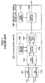
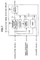
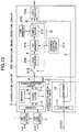
- This sort of synchronization equipment includes, as shown in Fig. 1, first and second analog-to-digital converters 101 and 102 to which in-phase components I-ch and orthogonal components Q-ch of a received signal obtained by synchronous detection of the received signal are inputted, respectively, a correlation circuit 103 to which the output signals of the first and second A/D converters 101 and 102 are inputted, and a reception timing detection circuit 108 to which the output signal of the correlation circuit 103 is inputted.
- the correlation circuit 103 includes a first memory 104 for storing the in-phase components I-ch and the orthogonal components Q-ch of M pieces of received signals having known patterns inputted from the first and second A/D converters 101 and 102, a correlator 105 to which two output signals of the first memory 104 are inputted, a second memory 106 where in-phase components and orthogonal components of known patterns belonging to the receiver are stored, and a power detection circuit 107 to which two output signals of the correlator 105 are inputted.
- the reception timing detection circuit 108 includes a memory 110 where a predetermined threshold value is stored, and a comparator 109 for comparing the output signal of the correlation circuit 103 and the threshold value stored in the memory 110 with each other.
- the in-phase components I-ch and the orthogonal components Q-ch of the received signal obtained by the synchronous detection of the received signal are quantized by the first and second A/D converters 101 and 102, and stored thereafter in the first memory 104 of the correlator circuit 103.
- the in-phase components I-ch and the orthogonal components Q-ch of M pieces of received signals having the known pattern can be stored by the fact that the in-phase components I-ch and the orthogonal components Q-ch of the received signal stored most previously are superscribed by the in-phase components I-ch and the orthogonal components Q-ch of a newly inputted received signal.
- two correlation values comb I and comb Q are computed with the following expressions using the in-phase components I-ch and orthogonal components Q-ch of the received signal outputted from the first memory 104 and the in-phase components and orthogonal components of the known pattern outputted from the second memory 106.
- Two correlation values comb I and comb Q computed in the correlator 105 are converted into one correlation value (power) comb by being processed in accordance with the following expression in the power detection circuit 107.
- comb comb I 2 + comb Q 2
- inferior letters I and Q show in-phase components and orthogonal components, respectively. Further, respective processings shown in the above-described expressions (1) to (3) can be realized simply by means of a software of a signal processor such as DSP.
- the correlation value obtained in the correlation circuit 103 is compared with the threshold value which has been stored in the third memory 110 in the comparator 109 of the reception timing detection circuit 108. When the correlation value obtained by the correlation circuit 103 is larger than this threshold value, it is decided that the known symbol has been received.
- the correlation value is normalized with the power of the received signal sometimes in order to oppress power variation of the correlation value by fading, but a structure in the case such normalization is not made is shown here.
- a first synchronization equipment of the present invention is a synchronization equipment for performing correlation processing between a first known pattern included in a received signal and a second known pattern to detect reception timing of the received signal, which comprises:
- a second synchronization equipment is the first synchronization equipment of the present invention described above, which further comprises timing correction value detection means for drawing up a histogram of reception time held in the latch circuit, compares the frequency of the reception time in the drawn up histogram with another threshold value, and generating a timing correction value for correcting the reception time sent by the reception window control means in accordance with the reception time when the frequency exceeds another threshold value.
- a third synchronization equipment of the present invention is a synchronization equipment for performing correlation processing between a first known pattern included in a received signal and a second known pattern to detect reception timing of the received signal, which comprises:
- a fourth synchronization equipment of the present invention is a synchronization equipment for performing correlation processing between a first known pattern included in a received signal and a second known pattern to detect reception timing of the received signal, which comprises:
- a fifth synchronization equipment of the present invention is a synchronization equipment for performing correlation processing between a first known pattern included in a received signal and a second known pattern to detect reception timing of the received signal, which comprises:
- a sixth synchronization equipment of the present invention is the fifth synchronization equipment of the present invention, in which the reception timing detection means comprises means which sustains comparison of the correlation value after the interpolation with the threshold value after deciding the reception time, and holds the reception time determined to be the reception timing.
- a seventh synchronisation equipment of the present invention is the fifth or sixth synchronization equipment of the present invention, further comprises timing lag detection means provided on the output side of the reception timing detection means, wherein the timing lag detection means comprises storage means where optimum reception time is stored and adding means for obtaining the difference between the reception time held by the reception timing detecting means and the optimum reception time.
- An eighth synchronization equipment of the present invention is the seventh synchronization equipment of the present invention, wherein the reception window control means comprises a counter for counting a clock and also being set an initial value in accordance with an output signal of the timing lag detection means.
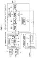
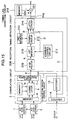
- a synchronization equipment includes, as shown in Fig. 3, first and second analog-to-digital converters (A/D converters) 1 and 2, a correlation circuit 3, a reception timing detection circuit 8, and a reception window control circuit 13.
- the first and second A/D converters 1 and 2 quantize in-phase components I-ch and orthogonal components Q-ch of a received signal obtained by synchronous detection of the received signal, respectively.
- the correlation circuit 3 computes a correlation value a between a known symbol pattern included in the output signals of the first and second A/D converters 1 and 2 and a known pattern belonging to a receiver, and includes a first memory 4 in which the in-phase components I-ch and orthogonal components Q-ch of the received signal inputted from the first and second A/D converters 1 and 2, respectively, are stored, a correlator 5 to which two output signals of the first memory 4 are inputted, a second memory 6 in which in-phase components I-ch and orthogonal components Q-ch of the known pattern of the receiver are stored, and a power detection circuit 7 to which two output signals of the correlator 5 are inputted.
- the reception timing detection circuit 8 decides that the known pattern in the received signal has been detected when the correlation value a computed in the correlation circuit 3 becomes larger than a predetermined threshold value, and includes a third memory 11 where the predetermined threshold value has been stored, a comparator 10 for comparing the output signal of the correlation circuit 3 with the predetermined threshold value stored in the memory 11, a switch 9 provided between the power detection circuit 7 and the comparator 10 and opening and closing of which is controlled by a timing correction control signal b outputted from the comparator 10, and a latch circuit 12 for latching a counter value c of a counter 14 described later of the reception window control circuit 13 by a timing correction control signal b outputted from the comparator 10.
- the reception window control circuit 13 operates the correlation circuit 3 and the reception timing detection circuit 8 only for a certain period of time, and includes the counter 14 to which a clock is inputted from the outside, and a decoder 15 for generating a timing detection window signal i which operates the correlation circuit 3 and the reception timing detection circuit 8 when the counter value c of the counter 14 shows a value of the time when the known symbol is received.
- the number of clocks inputted from the outside is counted with the counter 14 of the reception window control circuit 13.
- the count period of the counter 14 is the same as the reception interval of the known symbol.
- a timing detection window signal i is generated when the counter value c of the counter 14 shows a value of the time when the known symbol is received, and the correlation circuit 3 and the reception timing detection circuit 8 become operable only for the period that this timing detection window signal i is being generated.
- the in-phase components I-ch and the orthogonal components Q-ch of the received signal obtained by the synchronous detection of the received signal are quantized by the first and second A/D converters 1 and 2, and stored thereafter in the first memory 4 of the correlation circuit 3.
- first memory 4 in-phase components I-ch and orthogonal components Q-ch of M pieces of received signals having the known pattern can be stored, and the in-phase components I-ch and orthogonal components Q-ch of the received signal stored most previously are superscribed with in-phase components I-ch and orthogonal components Q-ch of a newly inputted received signal.
- two correlation values are computed with the above-mentioned expressions (1) and (2) using in-phase components I-ch and orthogonal components Q-ch of the received signal outputted from the first memory 4 and in-phase components and orthogonal components of the known pattern included in the receiver that are outputted from the second memory 6.
- Two correlation values computed in the correlator 5 are converted into one correlation value (power) a by being processed in the power detection circuit 7 in accordance with the above-mentioned expression (3).
- the correlation value a obtained in the correlation circuit 3 is inputted to the comparator 10 through the switch 9 of the reception timing detection circuit 8, and is compared with a predetermined threshold value stored in the third memory 11.
- a predetermined threshold value stored in the third memory 11.
- the timing correction control signal b is outputted from the comparator 10.
- the switch 9 is brought into an open state, and the detection of the known symbol is sustained.
- the timing correction control signal b is inputted to the latch circuit 12
- the counter value c of the counter 14 of the reception window control circuit 13 is introduced into the latch circuit 12.
- the switch 9 Since the switch 9 is kept in an open state hereafter, the correlation value a is never inputted to the reception timing detection circuit 8 from the correlation circuit 3, but the counter value c of the counter 14 which has been introduced in the latch circuit 12 is outputted as reception time tmg.
- the performance of equalization processing becomes better when the timing is adapted to the lead wave in general in an equalizer or the like that performs equalization processing of received data utilizing the reception timing detected in the synchronization equipment.
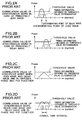
- the timing correction control signal b is outputted from the comparator 10 at the reception time t3 of the lead wave as shown in Fig. 4B. Since the switch 9 is brought to an open state by the timing correction control signal b at this time t3 and thereafter, the correlation value a computed in the correlation circuit 3 is never inputted to the comparator 10. As a result, the timing correction control signal b will never be outputted from the comparator 10 at the reception time t8 of the delay wave.
- the synchronization equipment it is possible to detect only the reception time of the lead wave even when there are peaks of correlation value larger than the predetermined threshold value at the reception time t3 of the lead wave and the reception time t8 of the delay wave in the reception window.
- the timing correction control signal b is outputted from the comparator 109 at the reception time t3 of the lead wave and at the reception time t8 of the delay wave as shown in Fig. 4C. Therefore, the reception timing is locked midway between the lead wave and the delay wave, thus producing the worst timing for the equalizer.
- the switch 9 for suspending detection of the known symbol when the known symbol is received and thereafter, and the latch circuit 12 for holding the time when the known symbol is received in the reception timing detection circuit 8 as described above it is possible to detect only the reception time of the lead wave surely even when the lead wave and the delay wave are in existence and there are the peaks of the correlation value larger than the predetermined threshold value in the reception window.
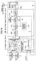
- a synchronization equipment according to a second embodiment of the present invention is different from the synchronization equipment according to the first embodiment shown in Fig. 3 in that a timing correction value detection circuit 16 is provided as shown in Fig. 5.
- the timing correction value detection circuit 16 includes a histogram circuit 17 to which the output signal of the latch circuit 12 of the reception timing detection circuit 8 is inputted, a fourth memory 19 in which a threshold value with respect to the frequency of reception timing has been stored, a comparator 18 for comparing the output signal of the histogram circuit 17 with the threshold value stored in the fourth memory 19, a fifth memory 21 in which the optimum reception time has been stored, and a correction value detection circuit 20 to which the output signal of the histogram circuit 17, the output signal (timing control signal d ) of the comparator 18 and the optimum reception time stored in the fifth memory 21 are inputted, and the output signal (counter correction value e ) of the correction value detection circuit 20 is inputted to the counter 14 of the reception window control circuit 13.
- the correlation circuit 3 and the reception timing detection circuit 8 in the synchronization equipment according to the present embodiment is similar to that of the synchronization equipment according to the first embodiment described above, the operation of the timing correction value detection circuit 16 and the reception window control circuit 13 related thereto will be described in detail hereinafter with reference to Figs. 6A and 6B.
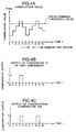
- the frequency of the reception timing is computed using the output signal of the latch circuit 12 of the reception timing detection circuit 8. For example, it is assumed that the histogram of the reception timing before update has the maximum value at time t3 as shown in Fig. 6A. When the newly detected reception timing is also at the time t3, 1 is added to the frequency at the time t3 until the last time in the histogram circuit 17 (see Fig. 6B).
- the comparator 18 the frequency at each time of the histogram computed in the histogram circuit 17 is compared with the threshold value stored in the fourth memory 19. In the comparator 18, when a frequency larger than the threshold value is in existence, the timing control signal d is outputted.
- the timing control signal d is outputted from the comparator 18 at the time t3.
- the time when the frequency becomes larger than the threshold value (the time t3 in the example shown in Fig. 6B) and the optimum reception time stored in the fifth memory 21 are compared with each other only when the timing control signal d is inputted from the comparator 18.
- the timing correction value e which sets the initial value of the counter 14 at -1 is outputted from the correction value detection circuit 20. Therefore, the reception time detected by the reception timing detection circuit 8 the next time becomes earlier than the actual reception time by one sample time interval and shows time t3 which is the optimum reception time.
- the timing correction value e which sets the initial value of the counter 14 at +1 is outputted from the correction value detection circuit 20. Therefore, the reception time detected by the reception timing detection circuit 8 next time gets later than the actual reception time by one sample time interval and shows time t3 which is the optimum reception time.
- the timing correction value detection circuit 16 which detects the histogram of the reception time and corrects the lag of the reception time when a frequency larger than the threshold value is included, it is possible to detect the reception time of the lead wave accurately even when both the lead wave and the delay wave are in existence.
- a synchronization equipment according to a third embodiment of the present invention is different from the synchronization equipment according to the first embodiment shown in Fig. 3 in that a reception timing detection circuit is structured as described hereunder.
- a reception timing detection circuit 31 includes a memory 32, a comparator 33, a timer 34, a maximum value detection circuit 35 and a latch circuit 36 as shown in Fig. 7.
- a predetermined threshold value is stored in the memory 32.
- a correlation value a sent from the correlation circuit 3 and the predetermined threshold value stored in the memory 32 are compared with each other, and 1 is outputted as a control signal f when the correlation value a is larger than the predetermined threshold value, and 0 is outputted as the control signal f when the correlation value a is smaller than the predetermined threshold value.
- a control signal g which operates the maximum value detection circuit 35 only for a certain period (timer value) is outputted.
- the maximum value detection circuit 35 when the newly inputted correlation value a is larger than the maximum value of the correlation values in the past, 1 is outputted as a control signal h only for a period shorter than one sample time interval, and the newly inputted correlation value a is also replaced with the maximum value of the correlation values in the past.
- the latch circuit 36 a count value c of the counter 14 of the reception window control circuit 13 is taken in and held at the rise edge of the control signal h from the maximum value detection circuit 35.
- the maximum value of the correlation values in the past stored in the maximum value detection circuit 35 is reset to 0 at a fall edge of an output signal (a timing detection window signal i ) of the decoder 15.
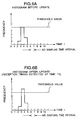
- the operation of the synchronization equipment according to the present embodiment will be described taking a case that the correlation value a and the predetermined threshold value stored in the memory 32 have a mutual relationship shown in Fig. 8A and the width of a timing detection window signal i is 4 as an example.
- the correlation value a becomes larger than the predetermined threshold value at time t1, 1 is outputted from the comparator 33 as the control signal f (see Fig. 8B).
- the timer value is set to 4 which is the width of the timing detection window signal i at the rise edge of the control signal f from the comparator 33 (see Fig. 8C)
- 1 is outputted from the timer 34 as the control signal g (see Fig. 8D).
- the maximum value detection circuit 35 starts the operation, and the maximum value of the correlation values in the past (0 in this case since it has been reset at the fall edge of the timing detection window signal i ) and the correlation value a computed at the time t1 are compared with each other.
- the control signal h having a pulse width shorter than one sample time interval is outputted from the maximum value detection circuit 35 (see Fig. 8E), and, in the maximum value detection circuit 35, the correlation value a computed at the time t1 is replaced with 0 which is the maximum value of the correlated values in the past.
- the counter value c is taken in and held at the rise edge of the control signal h .
- the correlation value a is larger than the predetermined threshold value at time t2, 1 is continued to be outputted from the comparator 33 as the control signal f (see Fig. 8B).
- the timer value is decremented and set to 3 (see Fig. 8C). Since the timer value is not 0 as before, however, 1 is continued to be outputted from the timer 34 as the control signal g (see Fig. 8D).
- the maximum value detection circuit 35 continues the operation, and the maximum value of the correlation values in the past (in this case, the correlation value a computed at the time t1) and the correlation value a computed at the time t2 are compared with each other.
- the control signal h having a pulse width shorter than one sample time interval is outputted from the maximum value detection circuit 35 (see Fig. 8E), and the correlation value a computed at the time t2 is replaced with the correlation value a computed at the time t1 in the maximum value detection circuit 35 at the same time.
- the counter value c is taken in and held at the rise edge of the control signal h .
- the control signal h having a pulse width shorter than one sample time interval is outputted from the maximum value detection circuit 35 (see Fig. 8E), and the correlation value a computed at the time t3 is replaced with the correlation value a computed at the time t2 in the maximum value detection circuit 35.
- the counter value c is taken in and held at the rise edge of the control signal h .
- the correlation value a is larger than the predetermined threshold value, 1 is continued to be outputted from the comparator 33 as the control signal f (see Fig. 8B).
- the timer value i decremented and set to 1 (see Fig. 8C). Since the timer value is not 0 as before, however, 1 is continued to be outputted from the timer 34 as the control signal g (see Fig. 8D).
- the maximum value detection circuit 35 continues the operation, and the maximum value among the correlation values in the past (in this case, the correlation value a computed at the time t3) and the correlation value a computed at the time t4 are compared with each other.
- the correlation value a computed at the time t4 is smaller than the correlation value a computed at the time t3, 0 is outputted from the maximum value detection circuit 35 as the control signal h (see Fig. 8E). At this time, the correlation value a computed at the time t4 is not replaced with the correlation value a computed at the time t3 in the maximum value detection circuit 35. Further, the latch circuit 36 continues to hold the counter value c taken in at the time t3.
- the correlation value a is smaller than the predetermined threshold value at time t5
- 0 is outputted from the comparator 33 as the control signal f (see Fig. 8B).
- the timer value is decremented and set to 0 (see Fig. 8C).
- 0 is outputted from the timer 34 as the control signal g (see Fig. 8D), and the operation of the maximum value detection circuit 35 is sustained. Further, the latch circuit 36 continues to hold the count value c taken in at the time t3.
- the maximum value detection circuit 35 Since 0 is continued to be outputted from the timer 34 as the control signal g from time t6 to time t10 (see Fig. 8D), the maximum value detection circuit 35 will never restart the operation. Further, the latch circuit 36 continues to hold the count value c taken in at the time t3. As a result, it is possible to detect the reception time of the lead wave accurately.
- the maximum value detection circuit 35 of the reception timing detection circuit 31 detects the reception time when the correlation value is at the maximum only during a certain period of time specified by the timer 34 from the time when the known symbol has been received and the latch circuit 36 holds the reception time after the lapse of the pointed time.
- the maximum value detection circuit 35 of the reception timing detection circuit 31 detects the reception time when the correlation value is at the maximum only during a certain period of time specified by the timer 34 from the time when the known symbol has been received and the latch circuit 36 holds the reception time after the lapse of the pointed time.
- a synchronization equipment according to a fourth embodiment of the present invention is different from the synchronization equipment according to the first embodiment shown in Fig. 3 in that a reception timing detection circuit is structured as described hereunder.
- a reception timing detection circuit 41 includes a switch 42, a memory 43, a comparator 44, first and second latch circuits 45 and 46, a mean circuit 47 and a window control circuit 48 as shown in Fig. 9.
- a predetermined threshold value is stored in the memory 43.
- the comparator 44 a correlation value a sent from the correlation circuit 3 through the switch 42 and the predetermined threshold value stored in the memory 43 are compared with each other, and 1 is outputted as a control signal j when the correlation value a is larger than the predetermined threshold value and 0 is outputted as the control signal j when the correlation value a is smaller than the predetermined threshold value.
- the counter value c of the counter 14 of the reception window control circuit 13 is taken in and held at the rise edge of the control signal j from the comparator 44.
- the counter value c is taken in and held at the fall edge of the control signal j from the comparator 44.
- the mean circuit 47 a mean value of the counter value c held in the first latch circuit 45 and the counter value c held in the second latch circuit 46 is obtained, and the obtained means value is used as the detection time of the known symbol.
- a switch control signal k which controls ON/OFF of the switch 42 is formed in the window control circuit 48.
- the switch control signal k is made 0 at the fall edge of the control signal j from the comparator 44 and is made 1 by the output signal (timing detection window signal i ) of the decoder 15.
- the switch 42 is turned OFF when the switch control signal k at 0 is inputted from the window control circuit 48 and is turned ON when the control signal k at 1 is inputted.
- the operation of the synchronization equipment according to the present embodiment will be described taking a case that the correlation value a and the predetermined threshold value stored in the memory 43 have a mutual relationship shown in Fig. 10A and the width of the timing detection window signal i is 4 as an example.
- the switch control signal k is set to 1 at time t0 by the timing detection window signal i (see Fig. 10C).
- the switch 42 is brought to an on-state (closed state).
- the comparator 44 the correlation value a which is sent from the correlation circuit 3 to the reception timing detection circuit 41 and the predetermined threshold value stored in the memory 43 are compared with each other. In this case, since the correlation value a is smaller than the predetermined threshold value (see Fig. 10A), 0 is outputted from the comparator 44 as the control signal j (see Fig. 10B).
- the counter value c is never taken in the first latch circuit 45 and the second latch circuit 46, and the outputs thereof become unstable (see Figs. 10D to 10G). With this, the output of the mean circuit 47 also becomes unstable.
- the switch control signal k Since the control signal j from the comparator 44 has no fall edge at time t1, the switch control signal k is remained as it is 1 (see Fig. 10C). As a result, the switch 42 remains ON (closed state).
- the switch control signal k Since the control signal j from the comparator 44 has no fall edge from time t2 to time t4, the switch control signal k is left as it is 1 (see Fig. 10C). As a result, the switch 42 remains in an ON-state (closed state).
- the correlation value a which is sent from the correlation circuit 3 to the reception timing detection circuit 41 and the predetermined threshold value stored in the memory 43 are compared with each other. In this case, since the correlation value a is larger than the predetermined threshold value (see Fig. 10A), 1 is continued to be outputted from the comparator 44 as the control signal j (see Fig. 10B).
- the counter value c is never taken in, but the output thereof remains as it is unsettled (see Figs. 10F and 10G).
- the output signal of the second latch circuit remains as it is unsettled.
- the switch 42 Since the switch 42 remains as it is ON at the time t5, the correlation value a sent from the correlation circuit 3 to the reception timing detection circuit 41 and the predetermined threshold value stored in the memory 43 are compared with each other. In this case, since the correlation value a is smaller than the predetermined threshold value (see Fig. 10A), the control signal j outputted from the comparator 44 is changed from 1 to 0 (see Fig. 10B). As a result, since a fall edge is produced in the control signal j from the comparator 44 and the switch control signal k is changed from 1 to 0 in the window control circuit 48 (see Fig. 10C), the switch 42 is brought to an OFF state (open state).
- the synchronization equipment according to the present embodiment since detection of the maximum value such as the synchronization equipment according to the third embodiment described above is not performed, it is possible to reduce the circuit scale when it is realized with a hardware or the number of operation steps when it is realized with a software. Further, since the same results are obtainable with a synchronization equipment according to the present embodiment and the synchronization equipment according to the above-mentioned third embodiment when the correlation value is symmetrical with respect to the reception time of the maximum value, it may safely be said that the synchronization equipment according to the present embodiment which is simple to be realized is preferable. When the correlation value is not symmetrical with respect to the reception time of the maximum value, however, the synchronization equipment according to the above-mentioned third embodiment can detect the reception time of the known reception symbol (the time when the correlation value reaches the maximum) more accurately.
- the detection timing is adapted to the lead wave when both the lead wave and the delay wave are received, it is possible to remove the effect by the delay wave thereby to detect the reception time of the lead wave accurately.
- a synchronization equipment according to a fifth embodiment of the present invention is different from the synchronization equipment according to the first embodiment shown in Fig. 3 in that a reception timing detection circuit is structured as described hereunder.
- a reception timing detection circuit 208 includes, as shown in Fig. 11, an interpolator 209 for interpolating the correlation value a which is sent from the correlation circuit 3, a first memory 210 in which a correlation value A after interpolation is stored, an address control circuit 211 for controlling the time and order for reading out the correlation value A after interpolation of the first memory 210, a second memory 213 in which a predetermined threshold value is stored, a comparator 212 for comparing the correlation value A after interpolation read out of the first memory 210 with the predetermined threshold value stored in the second memory 213, and outputting a control signal B when the correlation value A after interpolation is larger than the predetermined threshold value, and a latch circuit 214 for taking in and holding a counter value c which is sent from a reception window control circuit 13 and an interpolation number D which is sent from the address control circuit 211 when the control signal B is sent from the comparator 212.
- the operation of the synchronization equipment according to the present embodiment will be described taking a case that it is assumed that interpolation in the interpolator 209 is a three-times primary candidate, and the reception time of a known symbol is detected between the time t0 to the time t6 as an example.
- the output signal of the comparator 109 shows a high level during a period when the correlation value is larger than the threshold value (viz. from the time t3 to the time t4) as shown in Fig. 12B.
- the detection accuracy of the reception timing is determined univocally by a sampling time interval T in the first and second A/D converters 101 and 102.
- the correlation value a (see a broken line shown in Fig. 12C) outputted from the correlation circuit 3 is interpolated to three times in the interpolator 209, and the correlation value A after interpolation is stored in the first memory 210.
- the address control circuit 211 controls so as to read out the correlation value A after interpolation from the first memory 210 at the 0th, the first and the second of respective times (see a solid line shown in Fig. 12C), 0.1 and 2 are outputted from the address control circuit 211 to the latch circuit 214.
- the counter value c and the interpolation number D are taken in and held at the rise edge of the control signal B.
- n is a counter number
- a synchronization equipment according to a sixth embodiment of the present invention is different from the synchronization equipment according to the fifth embodiment shown in Fig. 11 in that a reception timing detection circuit 208A includes a switch 218 opening and closing of which is controlled by a control signal B outputted from the comparator 212 provided before the interpolator 209 as shown in Fig. 13.
- a correlation value a computed in the correlation circuit 3 changes with the passage of time as shown in Fig. 14A for instance.
- the lead wave is a received signal which reaches most immediately directly from a transmitting station
- the delay wave is a received signal which reaches late after reflected by a building, a mountain and so on.
- the lead wave is received principally
- a case when the delay wave is received principally there are a case when both the lead wave and the delay wave are received.
- the reception time of the lead wave is detected when the lead wave is received principally
- the reception time of the delay wave is detected when the delay wave is received principally
- both the reception time of the lead wave and the reception time of the delay wave are detected when both the lead wave and the delay wave are received.
- the reception timing when the reception timing is corrected based on the detected reception time, the reception timing is controlled a little to the delay wave between the lead wave and the delay wave. Therefore, the reception timing after control becomes a reception timing when the performance can be least demonstrated when the delay wave is going to be removed with an equalizer or the like.
- the synchronization equipment according to the present embodiment is capable of adapting the reception timing to the lead wave surely in order to give full display to the performance of an equalizer or the like.
- reception timing detection circuit 208A when the reception time of the known symbol is detected during time t0 to time t6 will be described hereinafter assuming that the interpolator 209 performs three times primary interpolation similarly to the case of the synchronization equipment according to the above-mentioned fifth embodiment.
- the switch 218 is closed on the rise edge of the output signal (a timing detection window signal i ) of the decoder 15 of the receiving window control circuit 13 at time t(0-0).
- the correlation value a computed in the correlation circuit 3 is inputted to the interpolator 209 and interpolation processing is performed, and stored thereafter in the first memory 210. That which has the interpolation number D of zero among the correlation values A after interpolation stored in the first memory 210 is selected in the address control circuit 211 and inputted to the comparator 212.
- the control signal B outputted from the comparator 212 remains as it is at a low level. Accordingly, in the latch circuit 214, the counter value c and the interpolation number D are never taken in.
- the counter value c (which indicates the time t2 in this case) and the interpolation number D (which indicates 2 in this case) are taken in and held at the rise edge of the control signal B. Further, the switch 218 is opened at the rise edge of the control signal B, and the switch 218 remains as it is opened thereafter.
- the correlation value a computed in the correlation circuit 3 is not inputted into an interpolator 209, but the control signal B outputted from the comparator 212 shows a low level (see Fig. 14C).
- the synchronization equipment according to the present embodiment it is possible to detect the reception timing of the lead wave surely even when both the lead wave and the delay wave are in existence in addition to the effect of synchronization equipment according to the above-mentioned fifth embodiment.
- the correlation value A after interpolation also exceeds the predetermined threshold value at the time t(4-2) as shown in Fig. 14B in the synchronization equipment according to the above-mentioned fifth embodiment, the latch circuit 214 is operated at the time t(4-2).
- the reception timing is locked midway between the lead wave and the delay wave.
- a synchronization equipment according to a seventh embodiment of the present invention is different from the synchronization equipment according to the sixth embodiment shown in Fig. 11 in that a timing lag detection circuit 219 is provided on the output side of the reception timing detection circuit 208 as shown in Fig. 15.
- the timing lag detection circuit 219 includes a memory 220 in which the optimum reception time is stored, and an adder 221 for obtaining the difference between the optimum reception time stored in the memory 220 and the reception time tmg detected in the reception timing detection circuit 208.
- the reception time tmg of the known symbol detected in the reception timing detection circuit 208 is expressed with the counter value c and the interpolation number D. Namely, when it is assumed that the counter value c of the counter 14 is n, the interpolation number D is m, the rate of interpolation is N, and the sampling time interval between the first and second A/D converters 1 and 2 is T, it is possible to obtain the reception time tmg with the above-mentioned expression (4). When it is assumed that the optimum reception time stored in the memory 220 is xT, the timing correction value ⁇ can be obtained from the following expression.
- timing lag detection circuit 219 is provided on the output side of the reception timing detection circuit 208A of the synchronization equipment according to the sixth embodiment shown in Fig. 13, similar effects are also obtainable.
- a synchronization equipment is different from the synchronization equipment according to the seventh embodiment shown in Fig. 15 in that an output signal H of the timing lag detection circuit 219 is inputted to a counter 14A of a receiving window control circuit 13A so as to correct timing automatically.
- the timing lag by the correlation value B after interpolation is corrected. Therefore, the timings of the first and second A/D converters 1 and 2 and a timing detection window signal f outputted from the decoder 15 are corrected with precision of T/N by using a clock having a frequency of a value obtained by multiplying sampling frequencies of the first and second A/D converters 1 and 2 by a rate of interpolation N as the clock inputted to the counter 14A.
- the counter 14A is operated at a period of reception intervals of the known symbol. It is possible to adjust the reception time backward and forward by adjusting the counter 14A.
- the synchronization equipment As described above, in the synchronization equipment according to the present embodiment, it is possible to correct the timing lag of a synchronizing signal automatically with a simple structure using the output signal H of the timing lag detection circuit 219 provided on the output side of the reception timing detection circuit 208.
- timing lag detection circuit 219 is provided on the output side of the reception timing detection circuit 208A of the synchronization equipment according to the sixth embodiment shown in Fig. 13, it is also possible to structure a synchronization equipment in which similar effects are obtainable.
Abstract
Description
- The present invention relates to a synchronization equipment used in digital communication. Description of the Related Art
- Conventionally, in this sort of synchronization equipment, a correlation value of a known pattern formed from a known symbol included in a received signal with a known pattern belonging to a receiver is computed, and it is decided that the known pattern has been detected when the computed correlation value becomes larger than a predetermined threshold value (disclosed in JP-A-7-250120 for instance).
- This sort of synchronization equipment includes, as shown in Fig. 1, first and second analog-to-
digital converters correlation circuit 103 to which the output signals of the first and second A/D converters timing detection circuit 108 to which the output signal of thecorrelation circuit 103 is inputted. Here, thecorrelation circuit 103 includes afirst memory 104 for storing the in-phase components I-ch and the orthogonal components Q-ch of M pieces of received signals having known patterns inputted from the first and second A/D converters correlator 105 to which two output signals of thefirst memory 104 are inputted, asecond memory 106 where in-phase components and orthogonal components of known patterns belonging to the receiver are stored, and apower detection circuit 107 to which two output signals of thecorrelator 105 are inputted. Further, the receptiontiming detection circuit 108 includes amemory 110 where a predetermined threshold value is stored, and acomparator 109 for comparing the output signal of thecorrelation circuit 103 and the threshold value stored in thememory 110 with each other. - In this synchronization equipment, the in-phase components I-ch and the orthogonal components Q-ch of the received signal obtained by the synchronous detection of the received signal are quantized by the first and second A/
D converters first memory 104 of thecorrelator circuit 103. In thefirst memory 104, the in-phase components I-ch and the orthogonal components Q-ch of M pieces of received signals having the known pattern can be stored by the fact that the in-phase components I-ch and the orthogonal components Q-ch of the received signal stored most previously are superscribed by the in-phase components I-ch and the orthogonal components Q-ch of a newly inputted received signal. - In the
correlator 105 of thecorrelation circuit 103, two correlation values combI and combQ are computed with the following expressions using the in-phase components I-ch and orthogonal components Q-ch of the received signal outputted from thefirst memory 104 and the in-phase components and orthogonal components of the known pattern outputted from thesecond memory 106.
- Two correlation values combI and combQ computed in the
correlator 105 are converted into one correlation value (power) comb by being processed in accordance with the following expression in thepower detection circuit 107.
- Besides, in the above-described expressions (1) to (3), inferior letters I and Q show in-phase components and orthogonal components, respectively. Further, respective processings shown in the above-described expressions (1) to (3) can be realized simply by means of a software of a signal processor such as DSP.
- The correlation value obtained in the
correlation circuit 103 is compared with the threshold value which has been stored in thethird memory 110 in thecomparator 109 of the receptiontiming detection circuit 108. When the correlation value obtained by thecorrelation circuit 103 is larger than this threshold value, it is decided that the known symbol has been received. - Besides, the correlation value is normalized with the power of the received signal sometimes in order to oppress power variation of the correlation value by fading, but a structure in the case such normalization is not made is shown here.
- In a synchronization equipment such as described above, however, there are such problems as shown hereunder.
- (1) Generally, when transmission is made including a known symbol train in a transmission signal, the correlation value shows the largest at the time when a transmitter transmits the known symbol train in an ideal state when the correlation between this known symbol train and the known symbol train belonging to a receiver is obtained. However, even when optimum timing is going to be detected from a fact that the correlation value simply becomes larger than a certain value or from a peak of the correlation value, the synchronization equipment does not necessarily operate smoothly when the received wave (hereinafter referred to as a "delay wave") which is received after reflected by a building or a mountain is in existence.
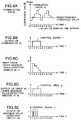
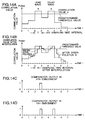
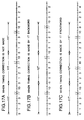
Namely, the correlation values when such a delay wave exists are shown in Figs. 2A to 2D for instance. When only a desired received wave (hereinafter referred to as a "lead wave" or a "desired wave") exists, it is possible to obtain timing which coincides with the lead wave accurately as shown in Fig. 2A. Further, when only a delay wave exists, it is possible to obtain timing which coincides with the delay wave accurately as shown in Fig. 2B. However, when the lead wave and the delay wave are in opposite phases and added to each other, the correlation value becomes small. Therefore, as shown in Fig. 2C, when the threshold value is made slightly larger, both the timing of the lead wave and the timing of the delay wave become no longer be detected. On the other hand, when the lead wave and the delay wave are in-phase and added to each other, the peak of the correlation value is detected at both of the reception time of the lead wave and the reception time of the delay wave. Therefore, as shown in Fig. 2D, the timing of the delay wave is detected only by the comparison with the threshold value. - (2) The detection accuracy of the reception timing is not so high. Namely, the detection accuracy of the reception timing depends on a sampling speed of the A/D converter, and it is when the lag between a transmitter and a receiver reaches T/2 (T: sampling time interval) that the detection accuracy is detected as a timing lag. When the sampling time interval is large, the timing lag becomes large, and the reception performance is deteriorated. Further, when the frequency discrepancy between the transmitter and the receiver is small even in case the sampling time interval is not so large, it takes time until the timing lag is detected and a state that the reception performance has been deteriorated to some extent is continued for long.
- It is an object of the present invention to provide a synchronization equipment which is capable of detecting reception time of a lead wave even when the lead wave and a delay wave exist at the same time in view of the problems described in the above item (1).
- It is another object of the present invention to provide a synchronization equipment which is capable of detecting reception timing with high accuracy in view of the problems described in the above item (2).
- A first synchronization equipment of the present invention is a synchronization equipment for performing correlation processing between a first known pattern included in a received signal and a second known pattern to detect reception timing of the received signal, which comprises:
- correlation value computing means for computing a correlation value between the first known pattern and the second known pattern;
- reception timing detecting means; and
- reception window control means for sending reception time to the correlation means and the reception timing detection means; wherein:
- the correlation value computing means computes the correlation value at every reception time; and
- the reception timing detection means compares the computed correlation value with a predetermined threshold value, decides the reception time when the computed correlation value becomes larger than the threshold value to be the reception timing of the received signal, suspends the comparison of the correlation value with the threshold value after the decision, and holds the reception time decided as the reception timing.
- A second synchronization equipment is the first synchronization equipment of the present invention described above, which further comprises timing correction value detection means for drawing up a histogram of reception time held in the latch circuit, compares the frequency of the reception time in the drawn up histogram with another threshold value, and generating a timing correction value for correcting the reception time sent by the reception window control means in accordance with the reception time when the frequency exceeds another threshold value.
- A third synchronization equipment of the present invention is a synchronization equipment for performing correlation processing between a first known pattern included in a received signal and a second known pattern to detect reception timing of the received signal, which comprises:
- correlation value computing means for computing a correlation value between the first known pattern and the second known pattern;
- reception timing detection means; and
- reception window control means for sending reception time to the correlation means and the reception timing detection means; wherein
- the correlation value computing means computes the correlation value at every reception time; and
- the reception timing detection means compares the computed correlation value with a predetermined threshold value, detects the reception time when the computed correlation value becomes larger than the threshold value, and obtains the reception time when the correlation value computed by the correlation value computing means becomes the largest during a certain period after the detected reception time and holds the reception time.
- A fourth synchronization equipment of the present invention is a synchronization equipment for performing correlation processing between a first known pattern included in a received signal and a second known pattern to detect reception timing of the received signal, which comprises:
- correlation value computing means for computing a correlation value between the first known pattern and the second known pattern;
- reception timing detection means; and
- reception window control means for sending reception time to the correlation means and the reception timing detection means; wherein:
- the correlation value computing means computes the correlation value at every reception time; and
- the reception timing detection means compares the computed correlation value with a predetermined threshold value, detects first reception time when the computed correlation value has become larger than the threshold value for the first time and second reception time when the computed correlation value has become smaller than the threshold value for the first time after the first reception time, and obtains a mean value of the first reception time and the second reception time and holds the mean value.
- A fifth synchronization equipment of the present invention is a synchronization equipment for performing correlation processing between a first known pattern included in a received signal and a second known pattern to detect reception timing of the received signal, which comprises:
- correlation value computing means for computing a correlation value between the first known pattern and the second known pattern;
- reception timing detection means; and
- reception window control means for sending reception time to the correlation means and the reception timing detection means; wherein:
- the correlation value computing means computes the correlation value at every reception time; and
- the reception timing detection means interpolates the computed correlation value, compares the correlation value after the interpolation with a predetermined threshold value, decides the reception time when the correlation value after the interpolation becomes larger than the threshold value to be the reception timing of the received signal.
- A sixth synchronization equipment of the present invention is the fifth synchronization equipment of the present invention, in which the reception timing detection means comprises means which sustains comparison of the correlation value after the interpolation with the threshold value after deciding the reception time, and holds the reception time determined to be the reception timing.
- A seventh synchronisation equipment of the present invention is the fifth or sixth synchronization equipment of the present invention, further comprises timing lag detection means provided on the output side of the reception timing detection means, wherein the timing lag detection means comprises storage means where optimum reception time is stored and adding means for obtaining the difference between the reception time held by the reception timing detecting means and the optimum reception time.
- An eighth synchronization equipment of the present invention is the seventh synchronization equipment of the present invention, wherein the reception window control means comprises a counter for counting a clock and also being set an initial value in accordance with an output signal of the timing lag detection means.
-
- Fig. 1 is a block diagram showing a conventional synchronization equipment;
- Figs. 2A to 2D show timing charts for explaining the operation of the synchronization equipment shown in Fig. 1;
- Fig. 3 is a block diagram of a synchronization equipment according to a first embodiment of the present invention;
- Figs. 4A to 4C are timing charts for explaining the operation of the synchronization equipment shown in Fig. 3;
- Fig. 5 is a block diagram of a synchronization equipment according to a second embodiment of the present invention;
- Figs. 6A and 6B are timing charts for explaining the operation of the synchronization equipment shown in Fig. 5;
- Fig. 7 is a block diagram of a synchronization equipment according to a third embodiment of the present invention;
- Figs. 8A to 8E are timing charts for explaining the operation of the synchronization equipment shown in Fig. 7;
- Fig. 9 is a block diagram of a synchronization equipment according to a fourth embodiment of the present invention;
- Figs. 10A to 10G are timing charts for explaining the operation of the synchronization equipment shown in Fig. 9;
- Fig. 11 is a block diagram of a synchronization equipment according to a fifth embodiment of the present invention;
- Figs. 12A to 12D are timing charts for explaining the operation of the synchronization equipment shown in Fig. 11;
- Fig. 13 is a block diagram of a synchronization equipment according to a sixth embodiment of the present invention;
- Figs. 14A to 14D are timing charts for explaining the operation of the synchronization equipment shown in Fig. 13;
- Fig. 15 is a block diagram of a synchronization equipment according to a seventh embodiment of the present invention;
- Fig. 16 is a block diagram of a synchronization equipment according to an eighth embodiment of the present invention; and
- Figs. 17A to 17C are timing charts for explaining the operation of the synchronization equipment shown in Fig. 16.
- A synchronization equipment according to a first embodiment of the present invention includes, as shown in Fig. 3, first and second analog-to-digital converters (A/D converters) 1 and 2, a
correlation circuit 3, a receptiontiming detection circuit 8, and a receptionwindow control circuit 13. The first and second A/D converters correlation circuit 3 computes a correlation value a between a known symbol pattern included in the output signals of the first and second A/D converters first memory 4 in which the in-phase components I-ch and orthogonal components Q-ch of the received signal inputted from the first and second A/D converters correlator 5 to which two output signals of thefirst memory 4 are inputted, asecond memory 6 in which in-phase components I-ch and orthogonal components Q-ch of the known pattern of the receiver are stored, and apower detection circuit 7 to which two output signals of thecorrelator 5 are inputted. The receptiontiming detection circuit 8 decides that the known pattern in the received signal has been detected when the correlation value a computed in thecorrelation circuit 3 becomes larger than a predetermined threshold value, and includes athird memory 11 where the predetermined threshold value has been stored, acomparator 10 for comparing the output signal of thecorrelation circuit 3 with the predetermined threshold value stored in thememory 11, aswitch 9 provided between thepower detection circuit 7 and thecomparator 10 and opening and closing of which is controlled by a timing correction control signal b outputted from thecomparator 10, and alatch circuit 12 for latching a counter value c of acounter 14 described later of the receptionwindow control circuit 13 by a timing correction control signal b outputted from thecomparator 10. The receptionwindow control circuit 13 operates thecorrelation circuit 3 and the receptiontiming detection circuit 8 only for a certain period of time, and includes thecounter 14 to which a clock is inputted from the outside, and adecoder 15 for generating a timing detection window signal i which operates thecorrelation circuit 3 and the receptiontiming detection circuit 8 when the counter value c of thecounter 14 shows a value of the time when the known symbol is received. - In the synchronization equipment of the present embodiment, the number of clocks inputted from the outside is counted with the
counter 14 of the receptionwindow control circuit 13. Here, the count period of thecounter 14 is the same as the reception interval of the known symbol. In thedecoder 15, a timing detection window signal i is generated when the counter value c of thecounter 14 shows a value of the time when the known symbol is received, and thecorrelation circuit 3 and the receptiontiming detection circuit 8 become operable only for the period that this timing detection window signal i is being generated. - The in-phase components I-ch and the orthogonal components Q-ch of the received signal obtained by the synchronous detection of the received signal are quantized by the first and second A/
D converters first memory 4 of thecorrelation circuit 3. In thefirst memory 4, in-phase components I-ch and orthogonal components Q-ch of M pieces of received signals having the known pattern can be stored, and the in-phase components I-ch and orthogonal components Q-ch of the received signal stored most previously are superscribed with in-phase components I-ch and orthogonal components Q-ch of a newly inputted received signal. In thecorrelator 5 of thecorrelation circuit 3, two correlation values are computed with the above-mentioned expressions (1) and (2) using in-phase components I-ch and orthogonal components Q-ch of the received signal outputted from thefirst memory 4 and in-phase components and orthogonal components of the known pattern included in the receiver that are outputted from thesecond memory 6. Two correlation values computed in thecorrelator 5 are converted into one correlation value (power) a by being processed in thepower detection circuit 7 in accordance with the above-mentioned expression (3). - The correlation value a obtained in the
correlation circuit 3 is inputted to thecomparator 10 through theswitch 9 of the receptiontiming detection circuit 8, and is compared with a predetermined threshold value stored in thethird memory 11. When the correlation value a obtained in thecorrelation circuit 3 is larger than this predetermined value, it is determined that the known symbol has been received, and the timing correction control signal b is outputted from thecomparator 10. When the timing correction control signal b is outputted from thecomparator 10, theswitch 9 is brought into an open state, and the detection of the known symbol is sustained. Further, when the timing correction control signal b is inputted to thelatch circuit 12, the counter value c of thecounter 14 of the receptionwindow control circuit 13 is introduced into thelatch circuit 12. Since theswitch 9 is kept in an open state hereafter, the correlation value a is never inputted to the receptiontiming detection circuit 8 from thecorrelation circuit 3, but the counter value c of thecounter 14 which has been introduced in thelatch circuit 12 is outputted as reception time tmg. - For example, as shown in Fig. 4A, when a lead wave and a delay wave are in existence and there are peaks of the correlation value larger than the predetermined threshold value at reception time t3 of the lead wave and reception time t8 of the delay wave in the reception window, the performance of equalization processing becomes better when the timing is adapted to the lead wave in general in an equalizer or the like that performs equalization processing of received data utilizing the reception timing detected in the synchronization equipment.
- In the synchronization equipment according to the present embodiment, since the correlation value a computed in the
correlation circuit 3 becomes larger than the predetermined threshold value at the reception time t3 of the lead wave, the timing correction control signal b is outputted from thecomparator 10 at the reception time t3 of the lead wave as shown in Fig. 4B. Since theswitch 9 is brought to an open state by the timing correction control signal b at this time t3 and thereafter, the correlation value a computed in thecorrelation circuit 3 is never inputted to thecomparator 10. As a result, the timing correction control signal b will never be outputted from thecomparator 10 at the reception time t8 of the delay wave. Accordingly, in the synchronization equipment according to the present embodiment, it is possible to detect only the reception time of the lead wave even when there are peaks of correlation value larger than the predetermined threshold value at the reception time t3 of the lead wave and the reception time t8 of the delay wave in the reception window. - On the other hand, in the conventional synchronization equipment shown in Fig. 1, when there are peaks of correlation value larger than the predetermined threshold value at the reception time t3 of the lead wave and the reception time t8 of the lead wave in the reception window, the timing correction control signal b is outputted from the
comparator 109 at the reception time t3 of the lead wave and at the reception time t8 of the delay wave as shown in Fig. 4C. Therefore, the reception timing is locked midway between the lead wave and the delay wave, thus producing the worst timing for the equalizer. - Since there are provided, in the synchronization equipment according to the present embodiment, the
switch 9 for suspending detection of the known symbol when the known symbol is received and thereafter, and thelatch circuit 12 for holding the time when the known symbol is received in the receptiontiming detection circuit 8 as described above, it is possible to detect only the reception time of the lead wave surely even when the lead wave and the delay wave are in existence and there are the peaks of the correlation value larger than the predetermined threshold value in the reception window. - A synchronization equipment according to a second embodiment of the present invention is different from the synchronization equipment according to the first embodiment shown in Fig. 3 in that a timing correction
value detection circuit 16 is provided as shown in Fig. 5. The timing correctionvalue detection circuit 16 includes ahistogram circuit 17 to which the output signal of thelatch circuit 12 of the receptiontiming detection circuit 8 is inputted, afourth memory 19 in which a threshold value with respect to the frequency of reception timing has been stored, acomparator 18 for comparing the output signal of thehistogram circuit 17 with the threshold value stored in thefourth memory 19, afifth memory 21 in which the optimum reception time has been stored, and a correctionvalue detection circuit 20 to which the output signal of thehistogram circuit 17, the output signal (timing control signal d) of thecomparator 18 and the optimum reception time stored in thefifth memory 21 are inputted, and the output signal (counter correction value e) of the correctionvalue detection circuit 20 is inputted to thecounter 14 of the receptionwindow control circuit 13. - Since the operation of the first and second A/
D converters correlation circuit 3 and the receptiontiming detection circuit 8 in the synchronization equipment according to the present embodiment is similar to that of the synchronization equipment according to the first embodiment described above, the operation of the timing correctionvalue detection circuit 16 and the receptionwindow control circuit 13 related thereto will be described in detail hereinafter with reference to Figs. 6A and 6B. - In the
histogram circuit 17 of the timing correctionvalue detection circuit 16, the frequency of the reception timing is computed using the output signal of thelatch circuit 12 of the receptiontiming detection circuit 8. For example, it is assumed that the histogram of the reception timing before update has the maximum value at time t3 as shown in Fig. 6A. When the newly detected reception timing is also at the time t3, 1 is added to the frequency at the time t3 until the last time in the histogram circuit 17 (see Fig. 6B). In thecomparator 18, the frequency at each time of the histogram computed in thehistogram circuit 17 is compared with the threshold value stored in thefourth memory 19. In thecomparator 18, when a frequency larger than the threshold value is in existence, the timing control signal d is outputted. Accordingly, in an example shown in Fig. 6B, since the frequency at the time t3 becomes larger than the threshold value, the timing control signal d is outputted from thecomparator 18 at the time t3. In the correctionvalue detection circuit 20, the time when the frequency becomes larger than the threshold value (the time t3 in the example shown in Fig. 6B) and the optimum reception time stored in thefifth memory 21 are compared with each other only when the timing control signal d is inputted from thecomparator 18. A timing correction value e which sets the initial value of thecounter 14 of the receptionwindow control circuit 13 at 0 in case the time when the frequency becomes larger than the threshold value is the same as the optimum reception time, sets the initial value of thecounter 14 at -1 in case the time when the frequency becomes larger than the threshold value is earlier than the optimum reception time, and sets the initial value of thecounter 14 at +1 in case the time when the frequency becomes larger than the threshold value is later than the optimum reception time is outputted from the correctionvalue detection circuit 20 to thecounter 14. - As a result, for example, in case the time when the frequency becomes larger than the threshold value is time t4 when the optimum reception time stored in the
fifth memory 21 is time t3, the timing correction value e which sets the initial value of thecounter 14 at -1 is outputted from the correctionvalue detection circuit 20. Therefore, the reception time detected by the receptiontiming detection circuit 8 the next time becomes earlier than the actual reception time by one sample time interval and shows time t3 which is the optimum reception time. On the other hand, in case the time when the frequency becomes larger than the threshold value is time t2 when the optimum reception time stored in thefifth memory 21 is time t3, the timing correction value e which sets the initial value of thecounter 14 at +1 is outputted from the correctionvalue detection circuit 20. Therefore, the reception time detected by the receptiontiming detection circuit 8 next time gets later than the actual reception time by one sample time interval and shows time t3 which is the optimum reception time. - Since there is provided, in the synchronization equipment of the present embodiment, the timing correction
value detection circuit 16 which detects the histogram of the reception time and corrects the lag of the reception time when a frequency larger than the threshold value is included, it is possible to detect the reception time of the lead wave accurately even when both the lead wave and the delay wave are in existence. - A synchronization equipment according to a third embodiment of the present invention is different from the synchronization equipment according to the first embodiment shown in Fig. 3 in that a reception timing detection circuit is structured as described hereunder.
- In the synchronization equipment according to the present embodiment, a reception
timing detection circuit 31 includes amemory 32, acomparator 33, atimer 34, a maximumvalue detection circuit 35 and alatch circuit 36 as shown in Fig. 7. In thememory 32, a predetermined threshold value is stored. In thecomparator 33, a correlation value a sent from thecorrelation circuit 3 and the predetermined threshold value stored in thememory 32 are compared with each other, and 1 is outputted as a control signal f when the correlation value a is larger than the predetermined threshold value, and 0 is outputted as the control signal f when the correlation value a is smaller than the predetermined threshold value. In thetimer 34, when 1 is inputted as the control signal f from thecomparator 33, a control signal g which operates the maximumvalue detection circuit 35 only for a certain period (timer value) is outputted. In the maximumvalue detection circuit 35, when the newly inputted correlation value a is larger than the maximum value of the correlation values in the past, 1 is outputted as a control signal h only for a period shorter than one sample time interval, and the newly inputted correlation value a is also replaced with the maximum value of the correlation values in the past. In thelatch circuit 36, a count value c of thecounter 14 of the receptionwindow control circuit 13 is taken in and held at the rise edge of the control signal h from the maximumvalue detection circuit 35. Besides, the maximum value of the correlation values in the past stored in the maximumvalue detection circuit 35 is reset to 0 at a fall edge of an output signal (a timing detection window signal i) of thedecoder 15. - The operation of the synchronization equipment according to the present embodiment will be described taking a case that the correlation value a and the predetermined threshold value stored in the
memory 32 have a mutual relationship shown in Fig. 8A and the width of a timing detection window signal i is 4 as an example. - Since the correlation value a is smaller than the predetermined threshold value at time t0, 0 is outputted from the
comparator 33 as the control signal f (see Fig. 8B). Further, since the timer value of thetimer 34 is 0 (see Fig. 8C), 0 is outputted from thetimer 34 as the control signal g (see Fig. 8D). As a result, the maximumvalue detection circuit 35 is not operated. - Since the correlation value a becomes larger than the predetermined threshold value at time t1, 1 is outputted from the
comparator 33 as the control signal f (see Fig. 8B). In thetimer 34, since the timer value is set to 4 which is the width of the timing detection window signal i at the rise edge of the control signal f from the comparator 33 (see Fig. 8C), 1 is outputted from thetimer 34 as the control signal g (see Fig. 8D). As a result, the maximumvalue detection circuit 35 starts the operation, and the maximum value of the correlation values in the past (0 in this case since it has been reset at the fall edge of the timing detection window signal i) and the correlation value a computed at the time t1 are compared with each other. Since the correlation value a computed at the time t1 is larger than 0, the control signal h having a pulse width shorter than one sample time interval is outputted from the maximum value detection circuit 35 (see Fig. 8E), and, in the maximumvalue detection circuit 35, the correlation value a computed at the time t1 is replaced with 0 which is the maximum value of the correlated values in the past. In thelatch circuit 36, the counter value c is taken in and held at the rise edge of the control signal h. - Since the correlation value a is larger than the predetermined threshold value at time t2, 1 is continued to be outputted from the
comparator 33 as the control signal f (see Fig. 8B). In thetimer 34, the timer value is decremented and set to 3 (see Fig. 8C). Since the timer value is not 0 as before, however, 1 is continued to be outputted from thetimer 34 as the control signal g (see Fig. 8D). As a result, the maximumvalue detection circuit 35 continues the operation, and the maximum value of the correlation values in the past (in this case, the correlation value a computed at the time t1) and the correlation value a computed at the time t2 are compared with each other. Since the correlation value a computed at the time t2 is larger than the correlation value a computed at the time t1, the control signal h having a pulse width shorter than one sample time interval is outputted from the maximum value detection circuit 35 (see Fig. 8E), and the correlation value a computed at the time t2 is replaced with the correlation value a computed at the time t1 in the maximumvalue detection circuit 35 at the same time. In thelatch circuit 36, the counter value c is taken in and held at the rise edge of the control signal h. - At time t3, 1 is continued to be outputted from the
comparator 33 as the control signal f (see Fig. 8B) because the correlation value a is larger than the predetermined threshold value. In thetimer 34, the timer value is decremented and set to 2 (see Fig. 8C). Since the timer value is not 0 as before, however, 1 is continued to be outputted from thetimer 34 as the control signal g (see Fig. 8D). As a result, the maximumvalue detection circuit 35 continues the operation, and the maximum value of the correlation values in the past (in this case, the correlation value a computed at the time t2) and the correlation value a computed at the time t3 are compared with each other. Since the correlation value a computed at the time t3 is larger than the correlation value a computed at the time t2, the control signal h having a pulse width shorter than one sample time interval is outputted from the maximum value detection circuit 35 (see Fig. 8E), and the correlation value a computed at the time t3 is replaced with the correlation value a computed at the time t2 in the maximumvalue detection circuit 35. In thelatch circuit 36, the counter value c is taken in and held at the rise edge of the control signal h. - At time t4, since the correlation value a is larger than the predetermined threshold value, 1 is continued to be outputted from the
comparator 33 as the control signal f (see Fig. 8B). In thetimer 34, the timer value i decremented and set to 1 (see Fig. 8C). Since the timer value is not 0 as before, however, 1 is continued to be outputted from thetimer 34 as the control signal g (see Fig. 8D). As a result, the maximumvalue detection circuit 35 continues the operation, and the maximum value among the correlation values in the past (in this case, the correlation value a computed at the time t3) and the correlation value a computed at the time t4 are compared with each other. Since the correlation value a computed at the time t4 is smaller than the correlation value a computed at the time t3, 0 is outputted from the maximumvalue detection circuit 35 as the control signal h (see Fig. 8E). At this time, the correlation value a computed at the time t4 is not replaced with the correlation value a computed at the time t3 in the maximumvalue detection circuit 35. Further, thelatch circuit 36 continues to hold the counter value c taken in at the time t3. - Since the correlation value a is smaller than the predetermined threshold value at time t5, 0 is outputted from the
comparator 33 as the control signal f (see Fig. 8B). In thetimer 34, the timer value is decremented and set to 0 (see Fig. 8C). As a result, 0 is outputted from thetimer 34 as the control signal g (see Fig. 8D), and the operation of the maximumvalue detection circuit 35 is sustained. Further, thelatch circuit 36 continues to hold the count value c taken in at the time t3. - Since 0 is continued to be outputted from the
timer 34 as the control signal g from time t6 to time t10 (see Fig. 8D), the maximumvalue detection circuit 35 will never restart the operation. Further, thelatch circuit 36 continues to hold the count value c taken in at the time t3. As a result, it is possible to detect the reception time of the lead wave accurately. - As described above, in the synchronization equipment according to the present embodiment, the maximum
value detection circuit 35 of the receptiontiming detection circuit 31 detects the reception time when the correlation value is at the maximum only during a certain period of time specified by thetimer 34 from the time when the known symbol has been received and thelatch circuit 36 holds the reception time after the lapse of the pointed time. Thus, it is possible to detect the reception time of the lead wave accurately even when the lead wave and the delay wave are in existence. - A synchronization equipment according to a fourth embodiment of the present invention is different from the synchronization equipment according to the first embodiment shown in Fig. 3 in that a reception timing detection circuit is structured as described hereunder.
- In the synchronization equipment according to the present embodiment, a reception
timing detection circuit 41 includes aswitch 42, amemory 43, acomparator 44, first andsecond latch circuits mean circuit 47 and awindow control circuit 48 as shown in Fig. 9. A predetermined threshold value is stored in thememory 43. In thecomparator 44, a correlation value a sent from thecorrelation circuit 3 through theswitch 42 and the predetermined threshold value stored in thememory 43 are compared with each other, and 1 is outputted as a control signal j when the correlation value a is larger than the predetermined threshold value and 0 is outputted as the control signal j when the correlation value a is smaller than the predetermined threshold value. In thefirst latch circuit 45, the counter value c of thecounter 14 of the receptionwindow control circuit 13 is taken in and held at the rise edge of the control signal j from thecomparator 44. In thesecond latch circuit 46, the counter value c is taken in and held at the fall edge of the control signal j from thecomparator 44. In themean circuit 47, a mean value of the counter value c held in thefirst latch circuit 45 and the counter value c held in thesecond latch circuit 46 is obtained, and the obtained means value is used as the detection time of the known symbol. A switch control signal k which controls ON/OFF of theswitch 42 is formed in thewindow control circuit 48. Here, the switch control signal k is made 0 at the fall edge of the control signal j from thecomparator 44 and is made 1 by the output signal (timing detection window signal i) of thedecoder 15. Theswitch 42 is turned OFF when the switch control signal k at 0 is inputted from thewindow control circuit 48 and is turned ON when the control signal k at 1 is inputted. - The operation of the synchronization equipment according to the present embodiment will be described taking a case that the correlation value a and the predetermined threshold value stored in the
memory 43 have a mutual relationship shown in Fig. 10A and the width of the timing detection window signal i is 4 as an example. - In the
window control circuit 48, the switch control signal k is set to 1 at time t0 by the timing detection window signal i (see Fig. 10C). As a result, theswitch 42 is brought to an on-state (closed state). In thecomparator 44, the correlation value a which is sent from thecorrelation circuit 3 to the receptiontiming detection circuit 41 and the predetermined threshold value stored in thememory 43 are compared with each other. In this case, since the correlation value a is smaller than the predetermined threshold value (see Fig. 10A), 0 is outputted from thecomparator 44 as the control signal j (see Fig. 10B). As a result, the counter value c is never taken in thefirst latch circuit 45 and thesecond latch circuit 46, and the outputs thereof become unstable (see Figs. 10D to 10G). With this, the output of themean circuit 47 also becomes unstable. - Since the control signal j from the
comparator 44 has no fall edge at time t1, the switch control signal k is remained as it is 1 (see Fig. 10C). As a result, theswitch 42 remains ON (closed state). In thecomparator 44, the correlation value a which is sent from thecorrelation circuit 3 to the receptiontiming detection circuit 41 and the predetermined threshold value stored in thememory 43 are compared with each other. In this case, since the correlation value a is larger than the predetermined threshold value (see Fig. 10A), 1 is outputted from thecomparator 44 as the control signal j (see Fig. 10B). As a result, in thefirst latch circuit 45, the counter value c (=1) is taken in at the rise edge of the control signal j (see Figs. 10D and 10E). On the other hand, in thesecond latch circuit 46, the counter value c is never taken in, but the output thereof remains as it is unsettled (see Figs. 10F and 10G). Although the counter value c (=1) is held in thefirst latch circuit 45, the output signal of the second latch circuit is unsettled. Therefore, the output of themean circuit 47 remains as it is unsettled. - Since the control signal j from the
comparator 44 has no fall edge from time t2 to time t4, the switch control signal k is left as it is 1 (see Fig. 10C). As a result, theswitch 42 remains in an ON-state (closed state). In thecomparator 44, the correlation value a which is sent from thecorrelation circuit 3 to the receptiontiming detection circuit 41 and the predetermined threshold value stored in thememory 43 are compared with each other. In this case, since the correlation value a is larger than the predetermined threshold value (see Fig. 10A), 1 is continued to be outputted from thecomparator 44 as the control signal j (see Fig. 10B). As a result, in thefirst latch circuit 45, the counter value c (=1) which was taken in at the time t1 is continued to be held (see Figs. 10D and 10E). On the other hand, in thesecond latch circuit 46, the counter value c is never taken in, but the output thereof remains as it is unsettled (see Figs. 10F and 10G). Although the counter value c (=1) which was taken in at the time t1 is continued to be held in thefirst latch circuit 45, the output signal of the second latch circuit remains as it is unsettled. - Since the
switch 42 remains as it is ON at the time t5, the correlation value a sent from thecorrelation circuit 3 to the receptiontiming detection circuit 41 and the predetermined threshold value stored in thememory 43 are compared with each other. In this case, since the correlation value a is smaller than the predetermined threshold value (see Fig. 10A), the control signal j outputted from thecomparator 44 is changed from 1 to 0 (see Fig. 10B). As a result, since a fall edge is produced in the control signal j from thecomparator 44 and the switch control signal k is changed from 1 to 0 in the window control circuit 48 (see Fig. 10C), theswitch 42 is brought to an OFF state (open state). Further, in thefirst latch circuit 45, the counter value c (=1) which was taken in at the time t1 continues to be held (see Figs. 10D and 10E), but the counter value c (=5) is taken in at the fall edge of the control signal j from thecomparator 44 in the second latch circuit 46 (see Figs. 10F and 10G). With this, a mean value (=3) of the counter value c (=1) taken into thefirst latch circuit 45 at the time t1 and the counter value c (=5) taken into thesecond latch circuit 46 is obtained for the output of themean circuit 47. - The switch control signal k remains as it is at 0 from time t6 to time t10 (see Fig. 10C). Accordingly, the correlation value a is never inputted to the
comparator 44, but 0 is inputted to thecomparator 44 in place of the correlation value a. Therefore, the control signal j outputted from thecomparator 44 remains as it is 0 (see Fig. 10B). As a result, the counter value c (=1) which was taken in at the time t1 continues to be held in thefirst latch circuit 45, and the counter value c (=5) which was taken in at the time t5 continues to be held in thesecond latch circuit 46. With this, the mean value (=3) obtained at the time t5 continues to be outputted from themean circuit 47. - As described above, in the synchronization equipment according to the present embodiment, the mean value of the first time when the correlation value a has become larger than the predetermined threshold value stored in the
memory 43 for the first time, detected in thefirst latch circuit 45 of the receptiontiming detection circuit 41, and the second time when the correlation value a becomes smaller than the predetermined threshold value for the first time after the first time, detected in thesecond latch circuit 46, is obtained in themean circuit 47, and this mean value is adopted as the reception time of the known symbol. Therefore, even when both the lead wave and the delay wave are in existence, it is possible to detect the reception time of the lead wave accurately. - Besides, in the synchronization equipment according to the present embodiment, since detection of the maximum value such as the synchronization equipment according to the third embodiment described above is not performed, it is possible to reduce the circuit scale when it is realized with a hardware or the number of operation steps when it is realized with a software. Further, since the same results are obtainable with a synchronization equipment according to the present embodiment and the synchronization equipment according to the above-mentioned third embodiment when the correlation value is symmetrical with respect to the reception time of the maximum value, it may safely be said that the synchronization equipment according to the present embodiment which is simple to be realized is preferable. When the correlation value is not symmetrical with respect to the reception time of the maximum value, however, the synchronization equipment according to the above-mentioned third embodiment can detect the reception time of the known reception symbol (the time when the correlation value reaches the maximum) more accurately.
- In the first to fourth embodiments of the present invention described above, since the detection timing is adapted to the lead wave when both the lead wave and the delay wave are received, it is possible to remove the effect by the delay wave thereby to detect the reception time of the lead wave accurately.
- A synchronization equipment according to a fifth embodiment of the present invention is different from the synchronization equipment according to the first embodiment shown in Fig. 3 in that a reception timing detection circuit is structured as described hereunder.
- In the synchronization equipment according to the present embodiment, a reception
timing detection circuit 208 includes, as shown in Fig. 11, aninterpolator 209 for interpolating the correlation value a which is sent from thecorrelation circuit 3, afirst memory 210 in which a correlation value A after interpolation is stored, anaddress control circuit 211 for controlling the time and order for reading out the correlation value A after interpolation of thefirst memory 210, asecond memory 213 in which a predetermined threshold value is stored, acomparator 212 for comparing the correlation value A after interpolation read out of thefirst memory 210 with the predetermined threshold value stored in thesecond memory 213, and outputting a control signal B when the correlation value A after interpolation is larger than the predetermined threshold value, and alatch circuit 214 for taking in and holding a counter value c which is sent from a receptionwindow control circuit 13 and an interpolation number D which is sent from theaddress control circuit 211 when the control signal B is sent from thecomparator 212. - The operation of the synchronization equipment according to the present embodiment will be described taking a case that it is assumed that interpolation in the
interpolator 209 is a three-times primary candidate, and the reception time of a known symbol is detected between the time t0 to the time t6 as an example. - In the conventional synchronization equipment shown in Fig. 1, when it is assumed that the correlation value outputted from the
correlation circuit 103 and the predetermined threshold value stored in thememory 110 have a relationship shown in Fig. 12A, the output signal of thecomparator 109 shows a high level during a period when the correlation value is larger than the threshold value (viz. from the time t3 to the time t4) as shown in Fig. 12B. Thus, in this synchronization equipment, the detection accuracy of the reception timing is determined univocally by a sampling time interval T in the first and second A/D converters - As against the above, in the synchronization equipment according to the present embodiment, the correlation value a (see a broken line shown in Fig. 12C) outputted from the
correlation circuit 3 is interpolated to three times in theinterpolator 209, and the correlation value A after interpolation is stored in thefirst memory 210. When theaddress control circuit 211 controls so as to read out the correlation value A after interpolation from thefirst memory 210 at the 0th, the first and the second of respective times (see a solid line shown in Fig. 12C), 0.1 and 2 are outputted from theaddress control circuit 211 to thelatch circuit 214. Now, when it is assumed that the correlation value A after interpolation and the predetermined threshold value stored in thesecond memory 213 have mutual relationship shown in Fig. 12C, the control signal B outputted from thecomparator 212 shows a high level during the period from an interpolation number D=2 at the time t3 when the correlation value A after interpolation becomes larger than the predetermined threshold value to an interpolation number D=0 at time t4 (see Fig. 12D). In thelatch circuit 214, the counter value c and the interpolation number D are taken in and held at the rise edge of the control signal B. With this, the detection time of the known symbol detected in the synchronization equipment according to the present embodiment is expressed by

- Here, n is a counter number,
- N is a rate of interpolation,
- m is an interpolation number, and
- T is a sampling time interval between the A/
D converters - A synchronization equipment according to a sixth embodiment of the present invention is different from the synchronization equipment according to the fifth embodiment shown in Fig. 11 in that a reception timing detection circuit 208A includes a
switch 218 opening and closing of which is controlled by a control signal B outputted from thecomparator 212 provided before theinterpolator 209 as shown in Fig. 13. - When the lead wave (a desired wave) and the delay wave are included in the received wave, a correlation value a computed in the
correlation circuit 3 changes with the passage of time as shown in Fig. 14A for instance. Here, the lead wave is a received signal which reaches most immediately directly from a transmitting station, and the delay wave is a received signal which reaches late after reflected by a building, a mountain and so on. In an electric wave environment where such a delay wave exists, there are a case when the lead wave is received principally, a case when the delay wave is received principally, and a case when both the lead wave and the delay wave are received. - Since only the lead wave is received when there is no delay wave, it is possible to cope with the circumstances sufficiently with the synchronization equipment according to the above-mentioned fifth embodiment. When the delay wave is in existence, however, since the time when the correlation value a becomes larger than the predetermined threshold value is adopted as the reception timing in the synchronization equipment according to the above-mentioned fifth embodiment, the reception time of the lead wave is detected when the lead wave is received principally, the reception time of the delay wave is detected when the delay wave is received principally, and both the reception time of the lead wave and the reception time of the delay wave are detected when both the lead wave and the delay wave are received. In such a case, when the reception timing is corrected based on the detected reception time, the reception timing is controlled a little to the delay wave between the lead wave and the delay wave. Therefore, the reception timing after control becomes a reception timing when the performance can be least demonstrated when the delay wave is going to be removed with an equalizer or the like. The synchronization equipment according to the present embodiment is capable of adapting the reception timing to the lead wave surely in order to give full display to the performance of an equalizer or the like.
- The operation of the reception timing detection circuit 208A when the reception time of the known symbol is detected during time t0 to time t6 will be described hereinafter assuming that the
interpolator 209 performs three times primary interpolation similarly to the case of the synchronization equipment according to the above-mentioned fifth embodiment. - When the time showing that the sampling time is n and the interpolation number D is m in the first and second A/
D converters switch 218 is closed on the rise edge of the output signal (a timing detection window signal i) of thedecoder 15 of the receivingwindow control circuit 13 at time t(0-0). As a result, the correlation value a computed in thecorrelation circuit 3 is inputted to theinterpolator 209 and interpolation processing is performed, and stored thereafter in thefirst memory 210. That which has the interpolation number D of zero among the correlation values A after interpolation stored in thefirst memory 210 is selected in theaddress control circuit 211 and inputted to thecomparator 212. Since the selected correlation value A after interpolation is smaller than the predetermined threshold value stored in thesecond memory 213 as shown in Fig. 14B, the control signal B outputted from thecomparator 212 remains as it is at a low level. Accordingly, in thelatch circuit 214, the counter value c and the interpolation number D are never taken in. - At time t(0-1), that which has the interpolation number D of 1 among the correlation values A after interpolation stored in the
first memory 210 is selected by theaddress control circuit 211 and inputted into thecomparator 212. Since this selected correlation value A after interpolation is smaller than the predetermined threshold value stored in thesecond memory 213 as shown in Fig. 14B, the control signal B outputted from thecomparator 212 remains as it is at a low level. Thus, in thelatch circuit 214, the counter value c and the interpolation number D are never taken in. - At time t(0-2), that which has the interpolation number D of 2 among the correlation values A after interpolation stored in the
first memory 210 is selected by theaddress control circuit 211 and inputted into thecomparator 212. Since this selected correlation value A after interpolation is smaller than the predetermined threshold value stored in thesecond memory 213 as shown in Fig. 14B, the control signal B outputted from thecomparator 212 remains as it is at a low level. Thus, in thelatch circuit 214, the counter value c and the interpolation number D are never taken in. - At time from time t(1-0) to time t(1-2), since the correlation value A after interpolation is smaller than the predetermined threshold value stored in the
second memory 213 as shown in Fig. 14B, the operation similar to that from the time t(0-0) to the time t(0-2) is performed. - At time from t(2-0) to t(2-1), since the correlation value A after interpolation is smaller than the predetermined threshold value stored in the
second memory 213 as shown in Fig. 14B, the operation similar to that at the above-mentioned time from time t(0-0) to time t(0-1) is performed. At time t(2-2), however, since the correlation value A after interpolation becomes larger than the predetermined value stored in thesecond memory 213 as shown in Fig. 14B, the control signal B outputted from thecomparator 212 shows a high level. Accordingly, in thelatch circuit 214, the counter value c (which indicates the time t2 in this case) and the interpolation number D (which indicates 2 in this case) are taken in and held at the rise edge of the control signal B. Further, theswitch 218 is opened at the rise edge of the control signal B, and theswitch 218 remains as it is opened thereafter. As a result, from time t(3-0) to time t(6-2), the correlation value a computed in thecorrelation circuit 3 is not inputted into aninterpolator 209, but the control signal B outputted from thecomparator 212 shows a low level (see Fig. 14C). As a result, time t(2-2) is outputted from thelatch circuit 214 as the receiving time of the known symbol after completion of timing detection window. With this, it is possible to detect the reception timing from the above-mentioned expression (4) with the accuracy of
- As described above, in the synchronization equipment according to the present embodiment, it is possible to detect the reception timing of the lead wave surely even when both the lead wave and the delay wave are in existence in addition to the effect of synchronization equipment according to the above-mentioned fifth embodiment. Incidentally, since the correlation value A after interpolation also exceeds the predetermined threshold value at the time t(4-2) as shown in Fig. 14B in the synchronization equipment according to the above-mentioned fifth embodiment, the
latch circuit 214 is operated at the time t(4-2). As a result, since reception timings of both the lead wave and the delay wave are detected as shown in Fig. 14D, the reception timing is locked midway between the lead wave and the delay wave. - A synchronization equipment according to a seventh embodiment of the present invention is different from the synchronization equipment according to the sixth embodiment shown in Fig. 11 in that a timing
lag detection circuit 219 is provided on the output side of the receptiontiming detection circuit 208 as shown in Fig. 15. Here, the timinglag detection circuit 219 includes amemory 220 in which the optimum reception time is stored, and anadder 221 for obtaining the difference between the optimum reception time stored in thememory 220 and the reception time tmg detected in the receptiontiming detection circuit 208. - As described previously, the reception time tmg of the known symbol detected in the reception
timing detection circuit 208 is expressed with the counter value c and the interpolation number D. Namely, when it is assumed that the counter value c of thecounter 14 is n, the interpolation number D is m, the rate of interpolation is N, and the sampling time interval between the first and second A/D converters memory 220 is xT, the timing correction value Δ can be obtained from the following expression.
adder 221. Namely, a negative timing correction value Δ is obtained when the reception time tmg of the known symbol is earlier than the optimum reception time xT, and a positive timing correction value Δ is obtained when the reception time tmg of the known symbol is later than the optimum reception time xT. Accordingly, in the synchronization equipment according to the present embodiment, it is possible to detect the reception timing lag from the output of the synchronization equipment with a simple structure. - Besides, when the timing
lag detection circuit 219 is provided on the output side of the reception timing detection circuit 208A of the synchronization equipment according to the sixth embodiment shown in Fig. 13, similar effects are also obtainable. - A synchronization equipment according to an eighth embodiment of the present invention is different from the synchronization equipment according to the seventh embodiment shown in Fig. 15 in that an output signal H of the timing
lag detection circuit 219 is inputted to acounter 14A of a receiving window control circuit 13A so as to correct timing automatically. In timing correction in the present embodiment, the timing lag by the correlation value B after interpolation is corrected. Therefore, the timings of the first and second A/D converters decoder 15 are corrected with precision of T/N by using a clock having a frequency of a value obtained by multiplying sampling frequencies of the first and second A/D converters counter 14A. Thecounter 14A is operated at a period of reception intervals of the known symbol. It is possible to adjust the reception time backward and forward by adjusting thecounter 14A. - A method of timing correction in the synchronization equipment according to the present embodiment will be described hereinafter with reference to Figs. 17A to 17C. Besides, it is assumed that the period of the
counter 14A is 11T on the convenience of explanation. - (1) When timing correction is not made:
As shown in Fig. 17A, the synchronization equipment is operated at the period of thecounter 14A (i.e. 11T). - (2) When timing correction is made backward:
For example, the reception time tmg of the known symbol is detected earlier than the optimum reception time (stored in the memory 220) by 1T, the output signal H of the timinglag detection circuit 219 shows a timing lag detection value of -1T. Since the whole is shifted backward as timing correction at this time, the initial value of thecounter 14A is set to -1T which is the timing lag detection value when the counter value c becomes (10+2/3)T as shown in Fig. 17B. - (3) When timing correction is made frontward:
For example, when the reception time tmg of the known symbol is detected later than the optimum reception time (stored in the memory 220) by 1T, the output signal H of the timinglag detection circuit 219 shows a timing lag detection value of +1T. Since the whole is shifted frontward as timing correction at this time, the initial value of thecounter 14A is set to +1T which is a timing lag detection value when the counter value c shows (10+2/3)T as shown in Fig. 17C. - As described above, in the synchronization equipment according to the present embodiment, it is possible to correct the timing lag of a synchronizing signal automatically with a simple structure using the output signal H of the timing
lag detection circuit 219 provided on the output side of the receptiontiming detection circuit 208. - Besides, when the timing
lag detection circuit 219 is provided on the output side of the reception timing detection circuit 208A of the synchronization equipment according to the sixth embodiment shown in Fig. 13, it is also possible to structure a synchronization equipment in which similar effects are obtainable. - In the synchronization equipments according to the fifth to eighth embodiments of the present invention described above, it is possible to detect the known symbol accurately, and to detect the reception timing with high accuracy by detecting the reception time of the known symbol after interpolating the correlation value computed in the correlation circuit.
Claims (16)
- A synchronization equipment for performing correlation processing between a first known pattern included in a received signal and a second known pattern to detect reception timing of said received signal, comprising:correlation value computing means (3) for computing a correlation value (a) between said first known pattern and said second known pattern;reception timing detection means (8); andreception window control means (13) for sending reception time to said correlation means (3) and said reception timing detection means (8); wherein:said correlation value computing means (3) computes said correlation value (a) at every reception time; andsaid reception timing detection means (8) compares said computed correlation value (a) with a predetermined threshold value, determines the reception time when said computed correlation value (a) becomes larger than said threshold value to be reception timing of said received signal, sustains the comparison between said correlation value (a) and said threshold value after said determination, and holds the reception time determined as said reception timing.
- A synchronization equipment according to Claim 1, wherein said reception timing detection means (8) comprises:a switch (9) to which said correlation value (a) is inputted from said correlation value computing means (3);a memory (11) in which said threshold value is stored;a comparator (10) for comparing said correlation value (a) inputted from said switch (9) with said threshold value, and outputting an output signal when said correlation value (a) becomes larger than said threshold value; anda latch circuit (12) for taking in and holding said reception time sent from said reception window control means (13) by the output signal of said comparator (10); wherein:said switch (9) is brought to an open state by the output signal of said comparator (10).
- A synchronization equipment according to Claim 1, further comprising timing correction value detection means (16) for drawing up a histogram of the reception time held in said latch circuit (12), comparing a frequency of the reception time in said drawn up histogram with another threshold value, and generating a timing correction value for correcting the reception time sent by said reception window control means (13).
- A synchronization equipment according to Claim 3, wherein said timing correction value detection means (16) comprises:a histogram drawing up circuit (17) for drawing up the histogram of the reception time held in said latch circuit (12);another memory (19) in which said another threshold value is stored;a comparator (18) for comparing the frequency of the reception time in said drawn up histogram with said another threshold value; anda timing correction value generating circuit (20) for generating the timing correction value for correcting the reception time sent by said reception window control means (13) in accordance with a reception time when said frequency exceeds another threshold value.
- A synchronization equipment for performing correlation processing between a first known pattern included in a received signal and a second known pattern to detect reception timing of said received signal, comprising:correlation value computing means (3) for computing a correlation value (a) between said first known pattern and said second known pattern;reception timing detection means (8); andreception window control means (13) for sending reception time to said correlation means (3) and said reception timing detection means (8); wherein:said correlation value computing means (3) computes said correlation value (a) at every reception time; andsaid reception timing detection means (8) compares said computed correlation value with a predetermined threshold value, detects reception time when said computed correlation value becomes larger than said threshold value, and obtains the reception time when the correlation value computed in said correlation value computing means (3) reaches the maximum during a certain period after said detected reception time.
- A synchronization equipment according to Claim 5, wherein said reception timing detection means (31) comprises:a memory (32) in which said threshold value is stored;a comparator (33) for comparing said correlation value inputted from said correlation value (a) computing means (3) with said threshold value and outputting an output signal (f) when said correlation value becomes larger than said threshold value;a timer (34) for generating an output signal (g) only for said certain period when the output signal of said comparator (33) is inputted;a maximum value detection circuit (35) for detecting a maximum value of the correlation value (a) inputted from said correlation value computing means (3) while the output signal of said timer (34) is being inputted and generating a control signal (h); anda latch circuit (36) for taking in said reception time which is sent from said reception window control means (13) and holding the reception time when said control signal is inputted from said maximum value detection circuit (35).
- A synchronization equipment for performing correlation processing between a first known pattern included in a received signal and a second known pattern to detect reception timing of said received signal, comprising:correlation value computing means (3) for computing a correlation value (a) between said first known pattern and said second known pattern;reception timing detection means (8); andreception window control means (13) for sending reception time to said correlation means (3) and said reception timing detection means (8); wherein:said correlation value computing means (3) computes said correlation value (a) at every reception time; andsaid reception timing detection means (31) compares said computed correlation value (a) with the predetermined threshold value, detects a first reception time when said computed correlation value becomes larger than said threshold value for the first time and a second reception time when said computed correlation value has become smaller than said threshold value for the first time after said first reception time, obtains a mean value of said first reception time and said second reception time, and holds said mean value.
- A synchronization equipment according to Claim 1, wherein said reception timing detection means (41) comprises:a switch (42) to which said correlation value (a) is inputted from said correlation value computing means (3);a memory (43) in which said threshold value is stored;a comparator (44) for comparing said correlation value inputted from said switch (42) with said threshold value, and outputting a first output signal when said correlation value becomes larger than the threshold value for the first time and also outputting a second output signal when said computed correlation value becomes smaller than said threshold value for the first time after said first reception time;a first latch circuit (45) for taking in and holding said reception time which is sent from said reception window control means (13) by the first output signal of said comparator (44);a second latch circuit (46) for taking in and holding said reception time which is sent from said reception window control means (13) by the second output signal of said comparator (44);a mean circuit (47) for obtaining a mean value of the reception time held in said first latch circuit (45) and the reception time held in said second latch circuit (46); anda window control circuit (48) for outputting a switch control signal (k) for bringing said switch (42) into an open state when said second output signal of said comparator (44) is inputted.
- A synchronization equipment for performing correlation processing between a first known pattern included in a received signal and a second known pattern to detect reception timing of said received signal, comprising:correlation value computing means (3) for computing a correlation value (a) between said first known pattern and said second known pattern;reception timing detection means (208); andreception window control means (13) for sending reception time to said correlation means (3) and said reception timing detection means (208); wherein:said correlation value computing means (3) computes said correlation value (a) at every reception time; andsaid reception timing detection means (208) interpolates said computed correlation value, compares said correlation value after said interpolation with the predetermined threshold value, and determines the reception time when the correlation value after said interpolation becomes larger than said threshold value to be reception timing of said received signal.
- A synchronization equipment according to Claim 9, wherein said reception timing detection means (208) comprises:an interpolator (209) for interpolating said computed correlation value;a first memory (210) in which said correlation value after interpolation is stored;an address control circuit (211) for controlling read-out of said correlation value after interpolation from said first memory (210) while corresponding to an interpolation number;a second memory (213) in which said threshold value is stored;a comparator (212) for comparing said correlation value after interpolation read out of said first memory (210) with said threshold value stored in said second memory (213), and outputting an output signal when said correlation value after interpolation becomes larger than said threshold value; anda latch circuit (214) for taking in and holding said reception time which is sent from said reception window control means (13) and said interpolation number (D) which is sent from said address control circuit (211) by the output signal of said comparator (212).
- A synchronization equipment according to Claim 9, wherein said reception timing detection means (208) comprises means for suspending the comparison between said correlation value after interpolation and said threshold value after said determination, and holding the reception time which is determined to be said reception timing.
- A synchronization equipment according to Claim 11, wherein said reception timing detection means (208A) further comprises a switch (218) provided on an input side of said interpolator, and opening and closing of which is controlled by the output signal of said comparator (212).
- A synchronization equipment according to Claim 9, further comprising timing lag detection means (219) provided on an output side of said reception timing detection means (208); whereinsaid timing lag detection means (219) comprises:storage means (220) in which the optimum reception time is stored; andadding means (221) for obtaining a difference between the reception time held by said reception timing detection means (208) and said optimum reception time.
- A synchronization equipment according to Claim 11, further comprising timing lag detection means (219) provided on an output side of said reception timing detection means (208); whereinsaid timing lag detection means (219) comprises:storage means (220) in which the optimum reception time is stored; andadding means (221) for obtaining a difference between the reception time held by said reception timing detection means (208) and said optimum reception time.
- A synchronization equipment according to Claim 13, wherein said reception window control means (13) comprises a counter (14) for counting a clock in which an initial value is set in accordance with an output signal of said timing lag detection means (219).
- A synchronization equipment according to Claim 14, wherein said reception window control means (13) comprises a counter (14A) for counting a clock in which an initial value is set in accordance with an output signal of said timing lag detection means (219).
Priority Applications (1)
| Application Number | Priority Date | Filing Date | Title |
|---|---|---|---|
| EP05018484A EP1598977A3 (en) | 1996-03-07 | 1997-03-06 | Synchronization equipment |
Applications Claiming Priority (6)
| Application Number | Priority Date | Filing Date | Title |
|---|---|---|---|
| JP50646/96 | 1996-03-07 | ||
| JP5064696 | 1996-03-07 | ||
| JP5064796 | 1996-03-07 | ||
| JP05064696A JP3447882B2 (en) | 1996-03-07 | 1996-03-07 | Synchronizer |
| JP05064796A JP3447883B2 (en) | 1996-03-07 | 1996-03-07 | Synchronizer |
| JP50647/96 | 1996-03-07 |
Related Child Applications (1)
| Application Number | Title | Priority Date | Filing Date |
|---|---|---|---|
| EP05018484A Division EP1598977A3 (en) | 1996-03-07 | 1997-03-06 | Synchronization equipment |
Publications (3)
| Publication Number | Publication Date |
|---|---|
| EP0794635A2 true EP0794635A2 (en) | 1997-09-10 |
| EP0794635A3 EP0794635A3 (en) | 2000-10-11 |
| EP0794635B1 EP0794635B1 (en) | 2007-01-10 |
Family
ID=26391109
Family Applications (2)
| Application Number | Title | Priority Date | Filing Date |
|---|---|---|---|
| EP05018484A Withdrawn EP1598977A3 (en) | 1996-03-07 | 1997-03-06 | Synchronization equipment |
| EP97103759A Expired - Lifetime EP0794635B1 (en) | 1996-03-07 | 1997-03-06 | Synchronization equipment |
Family Applications Before (1)
| Application Number | Title | Priority Date | Filing Date |
|---|---|---|---|
| EP05018484A Withdrawn EP1598977A3 (en) | 1996-03-07 | 1997-03-06 | Synchronization equipment |
Country Status (5)
| Country | Link |
|---|---|
| US (1) | US6289064B1 (en) |
| EP (2) | EP1598977A3 (en) |
| KR (1) | KR100246030B1 (en) |
| CN (1) | CN1136690C (en) |
| DE (1) | DE69737220T2 (en) |
Cited By (2)
| Publication number | Priority date | Publication date | Assignee | Title |
|---|---|---|---|---|
| GB2346776A (en) * | 1999-02-13 | 2000-08-16 | Motorola Ltd | Synchronisation lock detectors |
| EP1058434A2 (en) * | 1999-05-31 | 2000-12-06 | Sony Corporation | Symbol synchronisation in multicarrier receivers |
Families Citing this family (19)
| Publication number | Priority date | Publication date | Assignee | Title |
|---|---|---|---|---|
| US6185259B1 (en) * | 1996-06-12 | 2001-02-06 | Ericsson Inc. | Transmitter/receiver for GMSK and offset-QAM |
| FI101658B1 (en) * | 1996-12-12 | 1998-07-31 | Nokia Telecommunications Oy | Reception method and receiver |
| US6240132B1 (en) * | 1998-02-03 | 2001-05-29 | Adtran, Inc. | Mechanism for interpolating among samples of received communication signal using asynchronous high speed clock which is a nominal multiple of recovered signalling baud rate |
| US20020075972A1 (en) * | 2000-03-29 | 2002-06-20 | Time Domain Corporation | Apparatus, system and method for one-of-many positions modulation in an impulse radio communications system |
| DE60131824T2 (en) * | 2000-11-01 | 2008-11-27 | Ntt Docomo Inc. | Recovery of the symbol clock |
| CA2363927C (en) * | 2000-11-28 | 2004-07-06 | Research In Motion Limited | Synchronization signal detector and method |
| US7577188B1 (en) * | 2001-09-13 | 2009-08-18 | Cisco Technology, Inc. | Physical layer and MAC enhancements using complex sequences on a wireless channel |
| US7646831B2 (en) * | 2001-10-19 | 2010-01-12 | Nokia Corporation | Method and a device for controlling data extraction from a data stream containing at lease one data packet |
| US7394877B2 (en) * | 2001-12-20 | 2008-07-01 | Texas Instruments Incorporated | Low-power packet detection using decimated correlation |
| JP4016667B2 (en) * | 2002-02-15 | 2007-12-05 | ヤマハ株式会社 | Optical disc apparatus, focus control method and program |
| US6961413B2 (en) * | 2003-02-19 | 2005-11-01 | Sarakas Stephen T | Residential telephone system and method |
| EP1610575A4 (en) * | 2003-03-31 | 2010-07-21 | Fujitsu Ltd | Radio communication network and flow control method |
| TWI244277B (en) * | 2003-06-17 | 2005-11-21 | Benq Corp | Method for WCDMA frame synchronization and related device |
| EP1643657B1 (en) * | 2004-09-30 | 2008-05-14 | NTT DoCoMo, Inc. | Signal detector used in wireless communication system |
| CN100403822C (en) * | 2005-06-30 | 2008-07-16 | 华为技术有限公司 | Adaptive rate consulting device and method |
| JP4720658B2 (en) * | 2005-07-19 | 2011-07-13 | パナソニック株式会社 | Synchronization detection circuit and multi-mode wireless communication device |
| CN101043277B (en) * | 2007-04-29 | 2010-10-13 | Ut斯达康通讯有限公司 | Pulse synchronized method and unit in receptivity test of mobile communication terminal |
| US8170087B2 (en) * | 2007-05-10 | 2012-05-01 | Texas Instruments Incorporated | Correlation coprocessor |
| CN102035369B (en) * | 2009-09-30 | 2014-08-20 | 意法半导体研发(深圳)有限公司 | Negative charge pump with current protection |
Citations (3)
| Publication number | Priority date | Publication date | Assignee | Title |
|---|---|---|---|---|
| US5214617A (en) * | 1990-02-21 | 1993-05-25 | The Laitram Corporation | Hydroacoustic ranging system |
| US5359575A (en) * | 1993-09-08 | 1994-10-25 | The Laitram Corporation | Underwater pulse tracking system |
| US5473612A (en) * | 1994-11-28 | 1995-12-05 | Motorola, Inc. | Method and apparatus for minimizing false detection of packet data in a communication receiver |
Family Cites Families (14)
| Publication number | Priority date | Publication date | Assignee | Title |
|---|---|---|---|---|
| US3766315A (en) * | 1970-09-11 | 1973-10-16 | Nasa | Method and apparatus for a single channel digital communications system |
| US5016255A (en) * | 1989-08-07 | 1991-05-14 | Omnipoint Data Company, Incorporated | Asymmetric spread spectrum correlator |
| CA2045338C (en) * | 1990-06-26 | 1995-07-04 | Shousei Yoshida | Clock recovery circuit with open-loop phase estimator and wideband phase tracking loop |
| JPH05159462A (en) * | 1991-12-03 | 1993-06-25 | Canon Inc | Method for transmitting or recording information, information recording and reproducing device and information transmitting device |
| JP2877243B2 (en) | 1992-08-24 | 1999-03-31 | 日本電信電話株式会社 | Spread spectrum communication receiver |
| US5376894A (en) * | 1992-12-31 | 1994-12-27 | Pacific Communication Sciences, Inc. | Phase estimation and synchronization using a PSK demodulator |
| FR2707128B1 (en) * | 1993-06-29 | 1995-08-18 | Alcatel Telspace | Single word detection device modulated in BPSK adapted to an analog modem operating in TMDA mode and detection method implemented in such a device. |
| US5648991A (en) * | 1994-02-16 | 1997-07-15 | Kabushiki Kaisha Toshiba | Sampling phase synchronizing apparatus and bidirectional maximum likelihood sequence estimation scheme therefore |
| JP3097443B2 (en) * | 1994-02-28 | 2000-10-10 | ケイディディ株式会社 | Unique word detection method |
| JP2943839B2 (en) | 1994-03-08 | 1999-08-30 | 国際電気株式会社 | Frame synchronization circuit for equalizer |
| US5627863A (en) * | 1994-07-15 | 1997-05-06 | Amati Communications Corporation | Frame synchronization in multicarrier transmission systems |
| JPH0897748A (en) * | 1994-09-22 | 1996-04-12 | Toyota Central Res & Dev Lab Inc | Spread spectrum communication receiver |
| US5680421A (en) * | 1995-02-27 | 1997-10-21 | Oki Electric Industry Co., Ltd. | Frame synchronization apparatus |
| JP3073919B2 (en) * | 1995-12-30 | 2000-08-07 | 松下電器産業株式会社 | Synchronizer |
-
1997
- 1997-03-05 US US08/810,767 patent/US6289064B1/en not_active Expired - Lifetime
- 1997-03-06 EP EP05018484A patent/EP1598977A3/en not_active Withdrawn
- 1997-03-06 DE DE69737220T patent/DE69737220T2/en not_active Expired - Lifetime
- 1997-03-06 EP EP97103759A patent/EP0794635B1/en not_active Expired - Lifetime
- 1997-03-07 CN CNB971030502A patent/CN1136690C/en not_active Expired - Fee Related
- 1997-03-07 KR KR1019970007687A patent/KR100246030B1/en not_active IP Right Cessation
Patent Citations (3)
| Publication number | Priority date | Publication date | Assignee | Title |
|---|---|---|---|---|
| US5214617A (en) * | 1990-02-21 | 1993-05-25 | The Laitram Corporation | Hydroacoustic ranging system |
| US5359575A (en) * | 1993-09-08 | 1994-10-25 | The Laitram Corporation | Underwater pulse tracking system |
| US5473612A (en) * | 1994-11-28 | 1995-12-05 | Motorola, Inc. | Method and apparatus for minimizing false detection of packet data in a communication receiver |
Cited By (5)
| Publication number | Priority date | Publication date | Assignee | Title |
|---|---|---|---|---|
| GB2346776A (en) * | 1999-02-13 | 2000-08-16 | Motorola Ltd | Synchronisation lock detectors |
| GB2346776B (en) * | 1999-02-13 | 2001-09-12 | Motorola Ltd | Synchronisation lock detector and method |
| US6658075B1 (en) | 1999-02-13 | 2003-12-02 | Motorola, Inc. | Synchronization lock detector and method |
| EP1058434A2 (en) * | 1999-05-31 | 2000-12-06 | Sony Corporation | Symbol synchronisation in multicarrier receivers |
| EP1058434A3 (en) * | 1999-05-31 | 2002-07-24 | Sony Corporation | Symbol synchronisation in multicarrier receivers |
Also Published As
| Publication number | Publication date |
|---|---|
| DE69737220T2 (en) | 2007-10-25 |
| DE69737220D1 (en) | 2007-02-22 |
| EP0794635A3 (en) | 2000-10-11 |
| KR970068266A (en) | 1997-10-13 |
| CN1162883A (en) | 1997-10-22 |
| EP1598977A2 (en) | 2005-11-23 |
| KR100246030B1 (en) | 2000-04-01 |
| EP1598977A3 (en) | 2006-02-22 |
| CN1136690C (en) | 2004-01-28 |
| EP0794635B1 (en) | 2007-01-10 |
| US6289064B1 (en) | 2001-09-11 |
Similar Documents
| Publication | Publication Date | Title |
|---|---|---|
| EP0794635B1 (en) | Synchronization equipment | |
| US6792059B2 (en) | Early/on-time/late gate bit synchronizer | |
| US5940458A (en) | Method and compensating for time error of time/frequency generator using global positioning system | |
| EP0726662B1 (en) | Receiver and transmitter-receiver | |
| US5412698A (en) | Adaptive data separator | |
| JP3118548B2 (en) | Synchronous detection device and synchronization method for digital communication receiver | |
| EP0833476B1 (en) | Fast resynchronization system for high-speed data transmission | |
| EP0679307B1 (en) | Delay line separator for data bus | |
| US5706314A (en) | Joint maximum likelihood channel and timing error estimation | |
| EP0877505B1 (en) | Synchronous circuit controller for controlling data transmission between asynchronous circuits | |
| US5754606A (en) | Clock signal regenerating circuit | |
| JP3036854B2 (en) | Interference detection circuit | |
| CA1294334C (en) | Digital data separator | |
| US5717728A (en) | Data/clock recovery circuit | |
| CA2035774C (en) | Frame phase estimation method and circuit | |
| CZ256293A3 (en) | Method of modifying a clock resetting system being controlled by a decision, and apparatus for making the same | |
| US4672637A (en) | Adaptive bit synchronizer | |
| EP0481267B1 (en) | Frame alignment circuit | |
| EP0833478B1 (en) | Pattern matching apparatus | |
| US5396522A (en) | Method and apparatus for clock synchronization with information received by a radio receiver | |
| JPH10190619A (en) | Synchronizing device | |
| US6961397B2 (en) | Symbol synchronizer for impulse noise channels | |
| JP3251464B2 (en) | Clock recovery circuit | |
| US7161986B2 (en) | Data transmission system and data transmitter/receiver for use therein, and method thereof | |
| JP3447883B2 (en) | Synchronizer |
Legal Events
| Date | Code | Title | Description |
|---|---|---|---|
| PUAI | Public reference made under article 153(3) epc to a published international application that has entered the european phase |
Free format text: ORIGINAL CODE: 0009012 |
|
| 17P | Request for examination filed |
Effective date: 19970306 |
|
| AK | Designated contracting states |
Kind code of ref document: A2 Designated state(s): DE FR GB |
|
| PUAL | Search report despatched |
Free format text: ORIGINAL CODE: 0009013 |
|
| AK | Designated contracting states |
Kind code of ref document: A3 Designated state(s): DE FR GB |
|
| 17Q | First examination report despatched |
Effective date: 20050216 |
|
| RAP1 | Party data changed (applicant data changed or rights of an application transferred) |
Owner name: NTT MOBILE COMMUNICATIONS NETWORK INC. Owner name: PANASONIC MOBILE COMMUNICATIONS CO., LTD. |
|
| GRAP | Despatch of communication of intention to grant a patent |
Free format text: ORIGINAL CODE: EPIDOSNIGR1 |
|
| GRAS | Grant fee paid |
Free format text: ORIGINAL CODE: EPIDOSNIGR3 |
|
| GRAA | (expected) grant |
Free format text: ORIGINAL CODE: 0009210 |
|
| AK | Designated contracting states |
Kind code of ref document: B1 Designated state(s): DE FR GB |
|
| REG | Reference to a national code |
Ref country code: GB Ref legal event code: FG4D |
|
| REF | Corresponds to: |
Ref document number: 69737220 Country of ref document: DE Date of ref document: 20070222 Kind code of ref document: P |
|
| ET | Fr: translation filed | ||
| PLBE | No opposition filed within time limit |
Free format text: ORIGINAL CODE: 0009261 |
|
| STAA | Information on the status of an ep patent application or granted ep patent |
Free format text: STATUS: NO OPPOSITION FILED WITHIN TIME LIMIT |
|
| 26N | No opposition filed |
Effective date: 20071011 |
|
| PGFP | Annual fee paid to national office [announced via postgrant information from national office to epo] |
Ref country code: FR Payment date: 20140311 Year of fee payment: 18 |
|
| PGFP | Annual fee paid to national office [announced via postgrant information from national office to epo] |
Ref country code: GB Payment date: 20140305 Year of fee payment: 18 |
|
| PGFP | Annual fee paid to national office [announced via postgrant information from national office to epo] |
Ref country code: DE Payment date: 20140417 Year of fee payment: 18 |
|
| REG | Reference to a national code |
Ref country code: DE Ref legal event code: R119 Ref document number: 69737220 Country of ref document: DE |
|
| GBPC | Gb: european patent ceased through non-payment of renewal fee |
Effective date: 20150306 |
|
| REG | Reference to a national code |
Ref country code: FR Ref legal event code: ST Effective date: 20151130 |
|
| PG25 | Lapsed in a contracting state [announced via postgrant information from national office to epo] |
Ref country code: DE Free format text: LAPSE BECAUSE OF NON-PAYMENT OF DUE FEES Effective date: 20151001 Ref country code: GB Free format text: LAPSE BECAUSE OF NON-PAYMENT OF DUE FEES Effective date: 20150306 |
|
| PG25 | Lapsed in a contracting state [announced via postgrant information from national office to epo] |
Ref country code: FR Free format text: LAPSE BECAUSE OF NON-PAYMENT OF DUE FEES Effective date: 20150331 |