EP0795896A2 - Dry etching method - Google Patents
Dry etching method Download PDFInfo
- Publication number
- EP0795896A2 EP0795896A2 EP97400562A EP97400562A EP0795896A2 EP 0795896 A2 EP0795896 A2 EP 0795896A2 EP 97400562 A EP97400562 A EP 97400562A EP 97400562 A EP97400562 A EP 97400562A EP 0795896 A2 EP0795896 A2 EP 0795896A2
- Authority
- EP
- European Patent Office
- Prior art keywords
- dry etching
- film forming
- film
- group
- gaseous
- Prior art date
- Legal status (The legal status is an assumption and is not a legal conclusion. Google has not performed a legal analysis and makes no representation as to the accuracy of the status listed.)
- Withdrawn
Links
Images
Classifications
-
- H—ELECTRICITY
- H01—ELECTRIC ELEMENTS
- H01L—SEMICONDUCTOR DEVICES NOT COVERED BY CLASS H10
- H01L28/00—Passive two-terminal components without a potential-jump or surface barrier for integrated circuits; Details thereof; Multistep manufacturing processes therefor
- H01L28/40—Capacitors
- H01L28/55—Capacitors with a dielectric comprising a perovskite structure material
-
- H—ELECTRICITY
- H01—ELECTRIC ELEMENTS
- H01L—SEMICONDUCTOR DEVICES NOT COVERED BY CLASS H10
- H01L21/00—Processes or apparatus adapted for the manufacture or treatment of semiconductor or solid state devices or of parts thereof
- H01L21/02—Manufacture or treatment of semiconductor devices or of parts thereof
- H01L21/04—Manufacture or treatment of semiconductor devices or of parts thereof the devices having at least one potential-jump barrier or surface barrier, e.g. PN junction, depletion layer or carrier concentration layer
- H01L21/18—Manufacture or treatment of semiconductor devices or of parts thereof the devices having at least one potential-jump barrier or surface barrier, e.g. PN junction, depletion layer or carrier concentration layer the devices having semiconductor bodies comprising elements of Group IV of the Periodic System or AIIIBV compounds with or without impurities, e.g. doping materials
- H01L21/30—Treatment of semiconductor bodies using processes or apparatus not provided for in groups H01L21/20 - H01L21/26
- H01L21/302—Treatment of semiconductor bodies using processes or apparatus not provided for in groups H01L21/20 - H01L21/26 to change their surface-physical characteristics or shape, e.g. etching, polishing, cutting
- H01L21/306—Chemical or electrical treatment, e.g. electrolytic etching
-
- C—CHEMISTRY; METALLURGY
- C04—CEMENTS; CONCRETE; ARTIFICIAL STONE; CERAMICS; REFRACTORIES
- C04B—LIME, MAGNESIA; SLAG; CEMENTS; COMPOSITIONS THEREOF, e.g. MORTARS, CONCRETE OR LIKE BUILDING MATERIALS; ARTIFICIAL STONE; CERAMICS; REFRACTORIES; TREATMENT OF NATURAL STONE
- C04B41/00—After-treatment of mortars, concrete, artificial stone or ceramics; Treatment of natural stone
- C04B41/53—After-treatment of mortars, concrete, artificial stone or ceramics; Treatment of natural stone involving the removal of at least part of the materials of the treated article, e.g. etching, drying of hardened concrete
- C04B41/5338—Etching
- C04B41/5346—Dry etching
-
- H—ELECTRICITY
- H01—ELECTRIC ELEMENTS
- H01L—SEMICONDUCTOR DEVICES NOT COVERED BY CLASS H10
- H01L21/00—Processes or apparatus adapted for the manufacture or treatment of semiconductor or solid state devices or of parts thereof
- H01L21/02—Manufacture or treatment of semiconductor devices or of parts thereof
- H01L21/04—Manufacture or treatment of semiconductor devices or of parts thereof the devices having at least one potential-jump barrier or surface barrier, e.g. PN junction, depletion layer or carrier concentration layer
- H01L21/18—Manufacture or treatment of semiconductor devices or of parts thereof the devices having at least one potential-jump barrier or surface barrier, e.g. PN junction, depletion layer or carrier concentration layer the devices having semiconductor bodies comprising elements of Group IV of the Periodic System or AIIIBV compounds with or without impurities, e.g. doping materials
- H01L21/30—Treatment of semiconductor bodies using processes or apparatus not provided for in groups H01L21/20 - H01L21/26
- H01L21/31—Treatment of semiconductor bodies using processes or apparatus not provided for in groups H01L21/20 - H01L21/26 to form insulating layers thereon, e.g. for masking or by using photolithographic techniques; After treatment of these layers; Selection of materials for these layers
- H01L21/3105—After-treatment
- H01L21/311—Etching the insulating layers by chemical or physical means
- H01L21/31105—Etching inorganic layers
- H01L21/31111—Etching inorganic layers by chemical means
- H01L21/31116—Etching inorganic layers by chemical means by dry-etching
- H01L21/31122—Etching inorganic layers by chemical means by dry-etching of layers not containing Si, e.g. PZT, Al2O3
-
- H—ELECTRICITY
- H01—ELECTRIC ELEMENTS
- H01L—SEMICONDUCTOR DEVICES NOT COVERED BY CLASS H10
- H01L21/00—Processes or apparatus adapted for the manufacture or treatment of semiconductor or solid state devices or of parts thereof
- H01L21/02—Manufacture or treatment of semiconductor devices or of parts thereof
- H01L21/04—Manufacture or treatment of semiconductor devices or of parts thereof the devices having at least one potential-jump barrier or surface barrier, e.g. PN junction, depletion layer or carrier concentration layer
- H01L21/18—Manufacture or treatment of semiconductor devices or of parts thereof the devices having at least one potential-jump barrier or surface barrier, e.g. PN junction, depletion layer or carrier concentration layer the devices having semiconductor bodies comprising elements of Group IV of the Periodic System or AIIIBV compounds with or without impurities, e.g. doping materials
- H01L21/30—Treatment of semiconductor bodies using processes or apparatus not provided for in groups H01L21/20 - H01L21/26
- H01L21/31—Treatment of semiconductor bodies using processes or apparatus not provided for in groups H01L21/20 - H01L21/26 to form insulating layers thereon, e.g. for masking or by using photolithographic techniques; After treatment of these layers; Selection of materials for these layers
- H01L21/3205—Deposition of non-insulating-, e.g. conductive- or resistive-, layers on insulating layers; After-treatment of these layers
- H01L21/321—After treatment
- H01L21/3213—Physical or chemical etching of the layers, e.g. to produce a patterned layer from a pre-deposited extensive layer
- H01L21/32133—Physical or chemical etching of the layers, e.g. to produce a patterned layer from a pre-deposited extensive layer by chemical means only
- H01L21/32135—Physical or chemical etching of the layers, e.g. to produce a patterned layer from a pre-deposited extensive layer by chemical means only by vapour etching only
- H01L21/32136—Physical or chemical etching of the layers, e.g. to produce a patterned layer from a pre-deposited extensive layer by chemical means only by vapour etching only using plasmas
Definitions
- the present invention relates to a method for dry etching of various film structures used for making memory devices, in particular, floating-gate ferroelectric RAMs.
- film structures include ferroelectric materials such as lead zirco-titanate, strontium- or bismuth-based films, and electrode materials such as iridium or platinum/titanium group materials in a monolayer or laminated structure.
- ferroelectric RAM which is a type of non-volatile memory.
- Ferroelectric RAM owes its non-volatility to the use of memory devices made of a strongly dielectric material.
- flash memory devices which are ROM (Read Only Memory)
- ferroelectric memory devices are RAM (Random Access Memory), that is, ferroelectric RAM offers advantages such as its ability to freely access each bit and superior response speed.
- the ferroelectric RAM using floating gate is configured as a single transistor memory cell having a core structure of lead zirco-titanate (Pb(Zr x ⁇ Ti 1-x )O 3 , (abbreviated to PZT hereinbelow) sandwiched between electrodes of iridium/iridium dioxide film (abbreviated to Ir/IrO 2 hereinbelow). Adopting this construction has enabled to prevent diffusion and reaction of lead in PZT to lead to degradation of strong dielectric properties, thereby achieving a quantum increase in its rewriting capacity.
- PZT lead zirco-titanate
- Ir/IrO 2 iridium/iridium dioxide film
- This type of devices may also be made from, for example, strontium (Sr) based films such as SrTiO 3 , bismuth (Bi) based films such as Y1 (oxide mixture of Sr, Bi, Ta) for ferroelectric devices, and from platinum/titanium based films (referred to as Pt/Ti hereinbelow) for electrode structure.
- strontium (Sr) based films such as SrTiO 3
- bismuth (Bi) based films such as Y1 (oxide mixture of Sr, Bi, Ta) for ferroelectric devices
- Pt/Ti platinum/titanium based films
- the gaseous etchant is either chloride-based gases such as BCl 3 /Cl 2 or SiCl 4 , fluoride-based gases such as CF 4 , C 2 F 6 , a mixture of chloride-based and fluoride-based gases such as BCl 3 , Cl 2 and SF 6 , or bromide-based gases such as HBr.
- chloride-based gases such as BCl 3 /Cl 2 or SiCl 4
- fluoride-based gases such as CF 4 , C 2 F 6
- a mixture of chloride-based and fluoride-based gases such as BCl 3 , Cl 2 and SF 6
- bromide-based gases such as HBr.
- the method enables dry etching of a monolayer film structure or a laminated film structure made of a combination of materials typically represented by lead zirco-titanate based material, strontium-based material, bismuth-based material, which exhibit ferroelectric properties, and by iridium group and a platinum/titanium group materials suitable for forming electrodes.
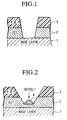
- Figure 1 is a schematic cross sectional view of a PZT film fabricated with a first embodiment of the dry etching method of the present invention.
- Figure 2 is a schematic cross sectional view of another PZT film fabricated with a conventional dry etching method.
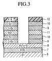
- Figure 3 is a schematic cross sectional view of a laminated PZT fabricated with a second embodiment of the dry etching method of the present invention.
- the first embodiment relates to a method of etching of a monolayer film structure of PZT.
- This is an example of a structure fabricated using photoresist masking in a reactive ion etching (referred to as RIE) apparatus of a parallel plate type.
- RIE reactive ion etching
- Figures 1 and 2 contrast the shapes of the fabricated cavities produced by the present method and by the conventional method, respectively.
- the film structure produced by the present process, shown in Figure 1 is comprised of a base layer 1, a PZT film 2, and a photoresist film 3.
- the conventional process using a mixture of gases SF6 and CHF3, produced deposit particles 4 on the PZT film 2, caused by the sulphur constituents in the etchant, as illustrated in Figure 2.
- the reaction products produced in the present process are PbCl 4 , ZrCl 4 and TiCl 4 as shown in equation (1), and, because all of the reaction products have relatively high vapor pressures, no unwanted deposit particles were formed on the etched surface as illustrated in Figure 1.
- etching gases other than BCl 3 , and Cl 2 can also be used successfully, for example, a mixture of chloride group gases such as SiCl 4 , fluoride group gases such as C 2 F 6 and bromide group gases such as HBr.
- HBr gas for instance, a volatile reaction product PbBr is again formed as in the case represented by equation (1).
- a second embodiment will be presented next. This is an example of dry etching a laminated film structure represented by Ir/IrO 2 /PZT/Ir/IrO 2 .
- Figure 3 is a schematic drawing of an example of a cavity fabricated in a laminated film structure.
- the laminated film structure comprises successive layers of: a SiO 2 film 7 serving as gate oxide layer formed on a silicon substrate base 6; followed by a polysilicon film 8 serving as a floating gate layer; followed by successive layers of IrO 2 film 9/Ir film 10 (electrodes)/ PZT film 11 (ferroelectric layer)/IrO 2 film 9/Ir film 10 (control gates).
- Etching process was carried out in the parallel plates RIE apparatus using a gaseous mixture of BCl 3 and Cl 2 and continuously etching the laminated film structure (i.e. Ir/IrO 2 /PZT/Ir/IrO 2 ) through a photoresist masking 12, as shown in Figure 3.
- the conditions for dry etching were the same as those in the first embodiment.
- This embodiment relates to dry etching of a structure comprising Ir/IrO 2 films.
- Etching trials using a photoresist making on Ir/IrO 2 films were carried out using the parallel plates RIE apparatus in two kinds of gaseous mixtures.
- First mixture contained Cl 2 and BCl 3 while the second mixture contained a suitable amount of SF 6 added to the Cl 2 /BCl 3 mixture.
- the conditions for dry etching were the same as those in the first embodiment.
- Etching trials using the second gas mixture demonstrated that a reaction product IrF 6 is produced during the dry etching process, because of the presence of SF 6 in the second gas mixture.
- the volatile IrF 6 does not adhere to the photoresist masking, therefore it is possible to perform dry etching while preventing the problem of rabbit ear formation.
- the masking film was etched away rapidly because the fluoride group gases readily attacked the photoresist material, and the difference in the etching rates on masking film and on the device structure resulted in a cavity having a slanted wall profile.
- the film structures which can be dry etched using the procedure disclosed are not limited to the materials and film structures mentioned in the foregoing embodiments.
- Other possibilities include monolayer or laminated film structures of single material or a combination of ferroelectric materials, such as PZT-based films including doped PZT, for example, PLZT ((Pb, La)(Zr, Ti)O 3 ), other lead oxide-based materials such as PTO (PbTiO 3 ), strontium-based materials such as SrTiO 3 , bismuth-based materials, electrode films such as Pt/Ti group films.
- PZT-based films including doped PZT, for example, PLZT ((Pb, La)(Zr, Ti)O 3 ), other lead oxide-based materials such as PTO (PbTiO 3 ), strontium-based materials such as SrTiO 3 , bismuth-based materials, electrode films such as Pt/Ti group films.
- a circle indicates a combination of etching film and etching gases which is practical
- a triangle indicates a combination of etching film and etching gases which is possible but presents some problems in practice (for example, etching rate is slow, formation of deposits etc.)
- a cross indicates a combination which is not workable.
- the present invention has demonstrated by experimental trials that a judicious choice of film material and etching gases enables dry etching to be carried out on many useful film materials as indicated partially in Table 1. It is important to recognize the basic principle that partial pressures of the reaction products constitute an important consideration in selecting a type of gas to be used in dry etching processes.
Abstract
A dry etching method is suitable for fabricating ferroelectric RAMs, a non-volatile memory, having a central core structure of PZT (a strong dielectric material) sandwiched between two electrodes (Ir/IrO2). The method is applicable to dry etching of a monolayer or laminated structure of a combination of ferroelectric films such as PZT-based, Sr-based, or Bi-based film as well as electrode structures of Ir or Pt/Ti group materials. The method utilizes a gaseous mixture of chloride-based gases such as BCl3 and Cl2, or SiCl4, or fluoride-based gases such as CF4, or C2F6 or a gaseous mixture of chloride- and fluoride-based gases, or bromide-based gases such as HBr. The method produces cavities having a high aspect ratio, free from products of reaction which are usually deposited on the cavity surfaces produced by the conventional dry etchants.
Description
- The present invention relates to a method for dry etching of various film structures used for making memory devices, in particular, floating-gate ferroelectric RAMs. Some examples of such film structures include ferroelectric materials such as lead zirco-titanate, strontium- or bismuth-based films, and electrode materials such as iridium or platinum/titanium group materials in a monolayer or laminated structure.
- In recent years, intensive research activities have been directed at developing ferroelectric RAMs which is a type of non-volatile memory. Ferroelectric RAM owes its non-volatility to the use of memory devices made of a strongly dielectric material. In contrast to flash memory devices which are ROM (Read Only Memory), ferroelectric memory devices are RAM (Random Access Memory), that is, ferroelectric RAM offers advantages such as its ability to freely access each bit and superior response speed.
- Especially, the ferroelectric RAM using floating gate is configured as a single transistor memory cell having a core structure of lead zirco-titanate (Pb(Zrx · Ti1-x)O3, (abbreviated to PZT hereinbelow) sandwiched between electrodes of iridium/iridium dioxide film (abbreviated to Ir/IrO2 hereinbelow). Adopting this construction has enabled to prevent diffusion and reaction of lead in PZT to lead to degradation of strong dielectric properties, thereby achieving a quantum increase in its rewriting capacity.
- However, in manufacturing such floating gate ferroelectric RAMs, the industry had no practical experience in photoresist masking and continuous dry etching of such laminated film structures as Ir/IrO2/PZT/Ir/IrO2.
- Regarding monolayer PZT structures used in various ferroelectric devices, a dry etching method using a gaseous mixture of SF6 and CHF3 has already been proposed. However, this method presents the following problems.
- (1) It is only possible to achieve etching rate of less than 50 nm/min, so that the productivity is low.
- (2) Deposit are formed on the etched surfaces, caused by the S component in SF6.
- (3) Etching selectivity against photoresist material is small, and anisotropic profile could not be produced.
- In spite of such problems, there has been no investigation of other alternative gaseous etchants.
- There has also been some parallel investigations of dry etching of Ir/IrO2 film structures containing no PZT, without coming to any satisfactory conclusion.
- This type of devices may also be made from, for example, strontium (Sr) based films such as SrTiO3, bismuth (Bi) based films such as Y1 (oxide mixture of Sr, Bi, Ta) for ferroelectric devices, and from platinum/titanium based films (referred to as Pt/Ti hereinbelow) for electrode structure. However, conventional semiconductor manufacturing technologies have not had extensive experience with such materials, and the present situation is that there is no practical method of dry etching such materials.
- It is an objective of the present invention to provide a dry etching method for a monolayer film structure or a laminated film structure of combination of ferroelectric materials such as PZT, Sr-, or Bi-based material, and electrode structures based on Ir and Pt/Ti group materials.
- The object has been achieved in a method in which the gaseous etchant is either chloride-based gases such as BCl3/Cl2 or SiCl4, fluoride-based gases such as CF4, C2F6, a mixture of chloride-based and fluoride-based gases such as BCl3, Cl2 and SF6, or bromide-based gases such as HBr. The method enables dry etching of a monolayer film structure or a laminated film structure made of a combination of materials typically represented by lead zirco-titanate based material, strontium-based material, bismuth-based material, which exhibit ferroelectric properties, and by iridium group and a platinum/titanium group materials suitable for forming electrodes.
- Figure 1 is a schematic cross sectional view of a PZT film fabricated with a first embodiment of the dry etching method of the present invention.
- Figure 2 is a schematic cross sectional view of another PZT film fabricated with a conventional dry etching method.
- Figure 3 is a schematic cross sectional view of a laminated PZT fabricated with a second embodiment of the dry etching method of the present invention.
- A first embodiment of the method will be presented below.
- The first embodiment relates to a method of etching of a monolayer film structure of PZT. This is an example of a structure fabricated using photoresist masking in a reactive ion etching (referred to as RIE) apparatus of a parallel plate type.
- It was decided to use a gaseous mixture of BCl3 and Cl2 (a chloride group gas) as the etchant, and operating the RIE apparatus under a set of conditions, for example: RF frequency of 13.56 MHz, RF power of 800 W, a pressure of 10∼20 mTorr, pedestal temperature of 10 °C, electrode gap of 30-80 mm, a ratio of flow rates of BCl3/Cl2 at 30 sccm/30 sccm.
- The chemical reaction taking place during the etching process is as follows:

- Figures 1 and 2 contrast the shapes of the fabricated cavities produced by the present method and by the conventional method, respectively. The film structure produced by the present process, shown in Figure 1, is comprised of a
base layer 1, aPZT film 2, and aphotoresist film 3. - The conventional process, using a mixture of gases SF6 and CHF3, produced deposit particles 4 on the
PZT film 2, caused by the sulphur constituents in the etchant, as illustrated in Figure 2. In contrast, the reaction products produced in the present process are PbCl4, ZrCl4 and TiCl4 as shown in equation (1), and, because all of the reaction products have relatively high vapor pressures, no unwanted deposit particles were formed on the etched surface as illustrated in Figure 1. - It was found that etching gases other than BCl3, and Cl2 can also be used successfully, for example, a mixture of chloride group gases such as SiCl4, fluoride group gases such as C2F6 and bromide group gases such as HBr. When using HBr gas, for instance, a volatile reaction product PbBr is again formed as in the case represented by equation (1).
- A second embodiment will be presented next. This is an example of dry etching a laminated film structure represented by Ir/IrO2/PZT/Ir/IrO2.
- Figure 3 is a schematic drawing of an example of a cavity fabricated in a laminated film structure. The laminated film structure comprises successive layers of: a SiO2 film 7 serving as gate oxide layer formed on a
silicon substrate base 6; followed by apolysilicon film 8 serving as a floating gate layer; followed by successive layers of IrO2 film 9/Ir film 10 (electrodes)/ PZT film 11 (ferroelectric layer)/IrO2film 9/Ir film 10 (control gates). - Etching process was carried out in the parallel plates RIE apparatus using a gaseous mixture of BCl3 and Cl2 and continuously etching the laminated film structure (i.e. Ir/IrO2/PZT/Ir/IrO2) through a
photoresist masking 12, as shown in Figure 3. The conditions for dry etching were the same as those in the first embodiment. - In this etching process also, it was possible to avoid the formation of deposit particles on the etched surface because of the formation of volatile reaction products through the use of BCl3 and Cl2. This process was also able to perform anisotropic etching.
- Next, a third embodiment will be presented.
- This embodiment relates to dry etching of a structure comprising Ir/IrO2 films.
- Etching trials using a photoresist making on Ir/IrO2 films were carried out using the parallel plates RIE apparatus in two kinds of gaseous mixtures. First mixture contained Cl2 and BCl3 while the second mixture contained a suitable amount of SF6 added to the Cl2/BCl3 mixture. The conditions for dry etching were the same as those in the first embodiment.
- There has not been any prior report on dry etching of Ir/IrO2 but it was found through these trials that dry etching was possible using the first gas mixture. However, it was also found that, during the step of removing the photoresist masking, Ir particles were redeposited on the side walls of the masking film to produce a deposit (known as rabbit ears), and this deposit presented a problem that it could not be removed by oxygen plasma processing to remove the photoresist masking.
- Etching trials using the second gas mixture demonstrated that a reaction product IrF6 is produced during the dry etching process, because of the presence of SF6 in the second gas mixture. The volatile IrF6 does not adhere to the photoresist masking, therefore it is possible to perform dry etching while preventing the problem of rabbit ear formation. When the amount of addition of SF6 was too low, rabbit ear formation took place, and when the amount was excessive, the masking film was etched away rapidly because the fluoride group gases readily attacked the photoresist material, and the difference in the etching rates on masking film and on the device structure resulted in a cavity having a slanted wall profile.
- It should be noted that, although SF6 was used in this embodiment as an additive gas, other similar type gases such as C2F6 produced the same result.
- It should also be noted that the film structures which can be dry etched using the procedure disclosed are not limited to the materials and film structures mentioned in the foregoing embodiments. Other possibilities include monolayer or laminated film structures of single material or a combination of ferroelectric materials, such as PZT-based films including doped PZT, for example, PLZT ((Pb, La)(Zr, Ti)O3), other lead oxide-based materials such as PTO (PbTiO3), strontium-based materials such as SrTiO3, bismuth-based materials, electrode films such as Pt/Ti group films. Combinations of primary candidates for film materials and etching gases are summarized in Table 1.
Table 1 Etching Gas Chloride-based Etchant Fluoride-based Etchant Chloride + Fluoride Bromide Etchant Film Material BCl3+Cl2 SiCl4 C2F6 CF4 BCl3+Cl2+SF6 HBr PZT-based PZT ○ ○ ○ ○ ○ ○ PLZT ○ ○ ○ ○ ○ Δ Sr-based SrTiO3 ○ Δ Δ X Δ ○ Bi-based Y1 ○ ○ Δ Δ ○ ○ Ir-group Ir/IrO2 Δ Δ Δ Δ ○ ○ Pt/Ti-group Pt/Ti ○ ○ X X Δ ○ - In Table 1, a circle indicates a combination of etching film and etching gases which is practical, a triangle indicates a combination of etching film and etching gases which is possible but presents some problems in practice (for example, etching rate is slow, formation of deposits etc.) and a cross indicates a combination which is not workable. The present invention has demonstrated by experimental trials that a judicious choice of film material and etching gases enables dry etching to be carried out on many useful film materials as indicated partially in Table 1. It is important to recognize the basic principle that partial pressures of the reaction products constitute an important consideration in selecting a type of gas to be used in dry etching processes.
Claims (8)
- A method for dry etching a monolayer structure of a film forming material or a laminated structure of a combination of film forming materials which is characterized by having the steps of:placing a film structure to be dry etched in a reactor vessel;admitting a gaseous etchant into said reactor vessel at a reduced pressure;performing dry etching to produce a cavity; andpreparing an etched device for further processing;wherein said gaseous etchant is a chloride-based gas, and said film forming material is selected from a group consisting of a lead zirco-titanate based material, a strontium-based material, a bismuth-based material, suitable for exhibiting ferroelectric properties, an iridium group material and a platinum/titanium group material suitable for forming electrodes.
- A method as claimed in claim 1, wherein said chloride-based gas includes a gaseous mixture of BCl3 and Cl2 or gaseous SiCl4.
- A method for dry etching a monolayer structure of a film forming material or a laminated structure of a combination of film forming materials which is characterized by having the steps of:placing a film structure to be dry etched in a reactor vessel;admitting a gaseous etchant into said reactor vessel at a reduced pressure;performing dry etching to produce a cavity; andpreparing an etched material for further processing;wherein said gaseous etchant is a fluoride-based gas, and said film forming material is selected from a group consisting of a lead zirco-titanate based material, a strontium-based material, a bismuth-based material, suitable for exhibiting ferroelectric properties, an iridium group material and a platinum/titanium group material suitable for forming electrodes.
- A method as claimed in claim 3, wherein said fluoride-based gas includes CF4 or C2F6.
- A method for dry etching a monolayer structure of a film forming material or a laminated structure of a combination of film forming materials which is characterized by having the steps of:placing a film structure to be dry etched in a reactor vessel;admitting a gaseous etchant into said reactor vessel at a reduced pressure;performing dry etching to produce a cavity; andpreparing an etched material for further processing;wherein said gaseous etchant is a mixture of a chloride-based gas and a fluoride-based gas, and said film forming material is selected from a group consisting of a lead zirco-titanate based material, a strontium-based material, a bismuth-based material, suitable for exhibiting ferroelectric properties, an iridium group material and a platinum/titanium group material suitable for forming electrodes.
- A method as claimed in claim 5, wherein said chloride-based gas includes a gaseous mixture of BCl3 and Cl2, or gaseous SiCl4, and said fluoride-based gas includes CF4, or C2F6.
- A method for dry etching a monolayer structure of a film forming material or a laminated structure of a film forming material which is characterized by having the steps of:placing a film structure to be dry etched in a reactor vessel;admitting a gaseous etchant into said reactor vessel at a reduced pressure;performing dry etching to produce a cavity; andpreparing an etched material for further processing;wherein said gaseous etchant is a bromide-based gas, and said film forming material is selected from a group consisting of a lead zirco-titanate based material, a strontium-based material, a bismuth-based material, suitable for exhibiting ferroelectric properties, an iridium group material and a platinum/titanium group material suitable for forming electrodes.
- A method as claimed in claim 7, wherein said bromide-based gas includes HBr.
Applications Claiming Priority (2)
| Application Number | Priority Date | Filing Date | Title |
|---|---|---|---|
| JP59696/96 | 1996-03-15 | ||
| JP8059696A JPH09251983A (en) | 1996-03-15 | 1996-03-15 | Dry etching method |
Publications (2)
| Publication Number | Publication Date |
|---|---|
| EP0795896A2 true EP0795896A2 (en) | 1997-09-17 |
| EP0795896A3 EP0795896A3 (en) | 1999-06-02 |
Family
ID=13120640
Family Applications (1)
| Application Number | Title | Priority Date | Filing Date |
|---|---|---|---|
| EP97400562A Withdrawn EP0795896A3 (en) | 1996-03-15 | 1997-03-13 | Dry etching method |
Country Status (4)
| Country | Link |
|---|---|
| EP (1) | EP0795896A3 (en) |
| JP (1) | JPH09251983A (en) |
| KR (1) | KR970067689A (en) |
| CA (1) | CA2199878A1 (en) |
Cited By (11)
| Publication number | Priority date | Publication date | Assignee | Title |
|---|---|---|---|---|
| FR2777114A1 (en) * | 1998-04-03 | 1999-10-08 | United Microelectronics Corp | METHOD OF ATTACKING A TANTALUM OXIDE LAYER |
| NL1009201C2 (en) * | 1998-05-06 | 1999-11-22 | United Microelectronics Corp | Method for etching a tantalum oxide layer. |
| US6037264A (en) * | 1997-03-13 | 2000-03-14 | Applied Materials, Inc. | Method for removing redeposited veils from etched platinum |
| US6265318B1 (en) | 1998-01-13 | 2001-07-24 | Applied Materials, Inc. | Iridium etchant methods for anisotropic profile |
| WO2001082344A2 (en) * | 2000-04-21 | 2001-11-01 | Applied Materials, Inc. | Method of patterning lead zirconium titanate and barium strontium titanate |
| US6323132B1 (en) | 1998-01-13 | 2001-11-27 | Applied Materials, Inc. | Etching methods for anisotropic platinum profile |
| US6482745B1 (en) | 1998-01-13 | 2002-11-19 | Applied Materials, Inc. | Etching methods for anisotropic platinum profile |
| US6485988B2 (en) * | 1999-12-22 | 2002-11-26 | Texas Instruments Incorporated | Hydrogen-free contact etch for ferroelectric capacitor formation |
| US6642567B1 (en) | 2000-08-31 | 2003-11-04 | Micron Technology, Inc. | Devices containing zirconium-platinum-containing materials and methods for preparing such materials and devices |
| WO2005022612A1 (en) * | 2003-09-03 | 2005-03-10 | Infineon Technologies Ag | Fence-free etching of iridium barrier having a steep taper angle |
| US6919168B2 (en) | 1998-01-13 | 2005-07-19 | Applied Materials, Inc. | Masking methods and etching sequences for patterning electrodes of high density RAM capacitors |
Families Citing this family (6)
| Publication number | Priority date | Publication date | Assignee | Title |
|---|---|---|---|---|
| KR100321703B1 (en) * | 1998-12-24 | 2002-03-08 | 박종섭 | A method for fabricating ferroelectric capacitor in semiconductor device |
| KR100321695B1 (en) * | 1998-12-30 | 2002-06-27 | 박종섭 | A method for fabricating ferroelectric capacitor in semiconductor device |
| KR100495913B1 (en) * | 2000-12-30 | 2005-06-17 | 주식회사 하이닉스반도체 | Method for fabricating semiconductor device |
| JP4551725B2 (en) | 2004-09-13 | 2010-09-29 | Okiセミコンダクタ株式会社 | Manufacturing method of semiconductor device |
| CN101203957B (en) | 2005-06-17 | 2011-03-30 | 富士通半导体股份有限公司 | Method for making semiconductor device |
| JP4999185B2 (en) * | 2008-03-04 | 2012-08-15 | 富士フイルム株式会社 | Dry etching method and dry etching apparatus |
Citations (5)
| Publication number | Priority date | Publication date | Assignee | Title |
|---|---|---|---|---|
| JPS6292323A (en) * | 1985-10-17 | 1987-04-27 | Nec Corp | Dry etching method |
| EP0587990A2 (en) * | 1992-07-27 | 1994-03-23 | Motorola, Inc. | Method for fabricating a semiconductive device having a conductive metal oxide |
| US5368687A (en) * | 1993-03-15 | 1994-11-29 | Micron Technology, Inc. | Semiconductor processing method of etching insulating inorganic metal oxide materials and method of cleaning metals from the surface of semiconductor wafers |
| US5443688A (en) * | 1993-12-02 | 1995-08-22 | Raytheon Company | Method of manufacturing a ferroelectric device using a plasma etching process |
| EP0725430A2 (en) * | 1995-02-03 | 1996-08-07 | Matsushita Electronics Corporation | Method of manufacturing semiconductor device having capacitor |
-
1996
- 1996-03-15 JP JP8059696A patent/JPH09251983A/en active Pending
-
1997
- 1997-03-13 CA CA002199878A patent/CA2199878A1/en not_active Abandoned
- 1997-03-13 EP EP97400562A patent/EP0795896A3/en not_active Withdrawn
- 1997-03-14 KR KR1019970008770A patent/KR970067689A/en not_active Application Discontinuation
Patent Citations (5)
| Publication number | Priority date | Publication date | Assignee | Title |
|---|---|---|---|---|
| JPS6292323A (en) * | 1985-10-17 | 1987-04-27 | Nec Corp | Dry etching method |
| EP0587990A2 (en) * | 1992-07-27 | 1994-03-23 | Motorola, Inc. | Method for fabricating a semiconductive device having a conductive metal oxide |
| US5368687A (en) * | 1993-03-15 | 1994-11-29 | Micron Technology, Inc. | Semiconductor processing method of etching insulating inorganic metal oxide materials and method of cleaning metals from the surface of semiconductor wafers |
| US5443688A (en) * | 1993-12-02 | 1995-08-22 | Raytheon Company | Method of manufacturing a ferroelectric device using a plasma etching process |
| EP0725430A2 (en) * | 1995-02-03 | 1996-08-07 | Matsushita Electronics Corporation | Method of manufacturing semiconductor device having capacitor |
Non-Patent Citations (3)
| Title |
|---|
| PATENT ABSTRACTS OF JAPAN vol. 011, no. 292 (E-543), 19 September 1987 & JP 62 092323 A (NEC CORP), 27 April 1987, * |
| POOR M R ET AL: "PLZT thin film etching using plasma techniques" 1990 IEEE 7TH INTERNATIONAL SYMPOSIUM ON APPLICATIONS OF FERROELECTRICS (CAT. NO. 90CH2800-1), URBANA-CHAMPAIGN, IL, USA, 6-8 JUNE 1990, ISBN 0-7803-0190-0, 1991, NEW YORK, NY, USA, IEEE, USA, pages 702-705, XP002082663 * |
| YOKOYAMA S ET AL: "HIGH-TEMPERATURE ETCHING IN PZT/PT/TIN STRUCTURE BY HIGH-DENSITY ECR PLASMA" JAPANESE JOURNAL OF APPLIED PHYSICS, vol. 34, no. 2B, PART 01, February 1995, pages 767-770, XP000599402 * |
Cited By (20)
| Publication number | Priority date | Publication date | Assignee | Title |
|---|---|---|---|---|
| US6037264A (en) * | 1997-03-13 | 2000-03-14 | Applied Materials, Inc. | Method for removing redeposited veils from etched platinum |
| US6277762B1 (en) | 1997-03-13 | 2001-08-21 | Applied Materials, Inc. | Method for removing redeposited veils from etched platinum |
| US6087265A (en) * | 1997-03-13 | 2000-07-11 | Applied Materials, Inc. | Method for removing redeposited veils from etched platinum |
| US6777342B2 (en) | 1998-01-13 | 2004-08-17 | Jeng H. Hwang | Method of plasma etching platinum |
| US6265318B1 (en) | 1998-01-13 | 2001-07-24 | Applied Materials, Inc. | Iridium etchant methods for anisotropic profile |
| US6919168B2 (en) | 1998-01-13 | 2005-07-19 | Applied Materials, Inc. | Masking methods and etching sequences for patterning electrodes of high density RAM capacitors |
| US6323132B1 (en) | 1998-01-13 | 2001-11-27 | Applied Materials, Inc. | Etching methods for anisotropic platinum profile |
| US6749770B2 (en) | 1998-01-13 | 2004-06-15 | Jeng H. Hwang | Method of etching an anisotropic profile in platinum |
| US6482745B1 (en) | 1998-01-13 | 2002-11-19 | Applied Materials, Inc. | Etching methods for anisotropic platinum profile |
| US6001742A (en) * | 1998-04-03 | 1999-12-14 | United Microelectronics Corp. | Method for etching tantalum oxide layer |
| FR2777114A1 (en) * | 1998-04-03 | 1999-10-08 | United Microelectronics Corp | METHOD OF ATTACKING A TANTALUM OXIDE LAYER |
| NL1009201C2 (en) * | 1998-05-06 | 1999-11-22 | United Microelectronics Corp | Method for etching a tantalum oxide layer. |
| US6485988B2 (en) * | 1999-12-22 | 2002-11-26 | Texas Instruments Incorporated | Hydrogen-free contact etch for ferroelectric capacitor formation |
| US6436838B1 (en) | 2000-04-21 | 2002-08-20 | Applied Materials, Inc. | Method of patterning lead zirconium titanate and barium strontium titanate |
| WO2001082344A3 (en) * | 2000-04-21 | 2002-02-28 | Applied Materials Inc | Method of patterning lead zirconium titanate and barium strontium titanate |
| WO2001082344A2 (en) * | 2000-04-21 | 2001-11-01 | Applied Materials, Inc. | Method of patterning lead zirconium titanate and barium strontium titanate |
| US6642567B1 (en) | 2000-08-31 | 2003-11-04 | Micron Technology, Inc. | Devices containing zirconium-platinum-containing materials and methods for preparing such materials and devices |
| US6946395B2 (en) | 2000-08-31 | 2005-09-20 | Micron Technology, Inc. | Devices containing zirconium-platinum-containing materials and methods for preparing such materials and devices |
| WO2005022612A1 (en) * | 2003-09-03 | 2005-03-10 | Infineon Technologies Ag | Fence-free etching of iridium barrier having a steep taper angle |
| US7015049B2 (en) | 2003-09-03 | 2006-03-21 | Infineon Technologies Ag | Fence-free etching of iridium barrier having a steep taper angle |
Also Published As
| Publication number | Publication date |
|---|---|
| EP0795896A3 (en) | 1999-06-02 |
| CA2199878A1 (en) | 1997-09-15 |
| KR970067689A (en) | 1997-10-13 |
| JPH09251983A (en) | 1997-09-22 |
Similar Documents
| Publication | Publication Date | Title |
|---|---|---|
| EP0795896A2 (en) | Dry etching method | |
| US6436838B1 (en) | Method of patterning lead zirconium titanate and barium strontium titanate | |
| EP1195803B1 (en) | Post-etch cleaning treatment | |
| DE19733391C2 (en) | Structuring process | |
| JP4562482B2 (en) | Ferroelectric capacitor structure and manufacturing method thereof | |
| US6432835B1 (en) | Process for fabricating an integrated circuit device having a capacitor with an electrode formed at a high aspect ratio | |
| JP3088178B2 (en) | Polysilicon film etching method | |
| US20080026539A1 (en) | Capacitance element manufacturing method and etching method | |
| US6417067B2 (en) | Method for fabricating an electrode structure of capacitor for semiconductor device | |
| KR19990006752A (en) | Etching method of electronic material thin film | |
| JP2000223666A (en) | Fabrication of semiconductor memory element | |
| US7045070B1 (en) | Method of producing an electrode configuration and method of electrically contacting the electrode configuration | |
| US6277760B1 (en) | Method for fabricating ferroelectric capacitor | |
| KR100289389B1 (en) | Capacitor fabrication method of semiconductor device | |
| KR20000067642A (en) | Method for dry-etching a ferroelectric capacitor structure | |
| KR100338808B1 (en) | Dry etching method of iridium electrode | |
| JP3166747B2 (en) | Method for manufacturing capacitor and capacitor | |
| JP2003224207A (en) | Semiconductor device and its fabricating method | |
| DE19929307C1 (en) | Structured layer, especially a FRAM capacitor lower electrode, is produced by heat treatment to cause layer material migration from a migration region to a target region of a substrate | |
| US7015049B2 (en) | Fence-free etching of iridium barrier having a steep taper angle | |
| DE112004000192T5 (en) | Hard mask with high selectivity for IR barrier layers for the production of a ferroelectric capacitor | |
| US20020119669A1 (en) | Method of fabricating semiconductor device | |
| US5292402A (en) | Masking material for applications in plasma etching | |
| KR100468698B1 (en) | Etching gas for ferroelectric film and fabrication method for ferroelectric capacitor using the same | |
| WO2001001462A1 (en) | Method for producing a noble-metal electrode |
Legal Events
| Date | Code | Title | Description |
|---|---|---|---|
| PUAI | Public reference made under article 153(3) epc to a published international application that has entered the european phase |
Free format text: ORIGINAL CODE: 0009012 |
|
| 17P | Request for examination filed |
Effective date: 19970318 |
|
| AK | Designated contracting states |
Kind code of ref document: A2 Designated state(s): DE FR GB |
|
| PUAL | Search report despatched |
Free format text: ORIGINAL CODE: 0009013 |
|
| AK | Designated contracting states |
Kind code of ref document: A3 Designated state(s): DE FR GB |
|
| STAA | Information on the status of an ep patent application or granted ep patent |
Free format text: STATUS: THE APPLICATION IS DEEMED TO BE WITHDRAWN |
|
| 18D | Application deemed to be withdrawn |
Effective date: 19991001 |