EP0796005B1 - Electronic camera using a small sensor with high speed imaging - Google Patents
Electronic camera using a small sensor with high speed imaging Download PDFInfo
- Publication number
- EP0796005B1 EP0796005B1 EP97301517A EP97301517A EP0796005B1 EP 0796005 B1 EP0796005 B1 EP 0796005B1 EP 97301517 A EP97301517 A EP 97301517A EP 97301517 A EP97301517 A EP 97301517A EP 0796005 B1 EP0796005 B1 EP 0796005B1
- Authority
- EP
- European Patent Office
- Prior art keywords
- imaging device
- electronic camera
- imaging
- subscanning
- camera according
- Prior art date
- Legal status (The legal status is an assumption and is not a legal conclusion. Google has not performed a legal analysis and makes no representation as to the accuracy of the status listed.)
- Expired - Lifetime
Links
Images


Classifications
-
- H—ELECTRICITY
- H04—ELECTRIC COMMUNICATION TECHNIQUE
- H04N—PICTORIAL COMMUNICATION, e.g. TELEVISION
- H04N3/00—Scanning details of television systems; Combination thereof with generation of supply voltages
- H04N3/02—Scanning details of television systems; Combination thereof with generation of supply voltages by optical-mechanical means only
- H04N3/08—Scanning details of television systems; Combination thereof with generation of supply voltages by optical-mechanical means only having a moving reflector
-
- H—ELECTRICITY
- H04—ELECTRIC COMMUNICATION TECHNIQUE
- H04N—PICTORIAL COMMUNICATION, e.g. TELEVISION
- H04N25/00—Circuitry of solid-state image sensors [SSIS]; Control thereof
- H04N25/70—SSIS architectures; Circuits associated therewith
- H04N25/71—Charge-coupled device [CCD] sensors; Charge-transfer registers specially adapted for CCD sensors
- H04N25/711—Time delay and integration [TDI] registers; TDI shift registers
-
- H—ELECTRICITY
- H04—ELECTRIC COMMUNICATION TECHNIQUE
- H04N—PICTORIAL COMMUNICATION, e.g. TELEVISION
- H04N23/00—Cameras or camera modules comprising electronic image sensors; Control thereof
- H04N23/50—Constructional details
- H04N23/55—Optical parts specially adapted for electronic image sensors; Mounting thereof
-
- H—ELECTRICITY
- H04—ELECTRIC COMMUNICATION TECHNIQUE
- H04N—PICTORIAL COMMUNICATION, e.g. TELEVISION
- H04N25/00—Circuitry of solid-state image sensors [SSIS]; Control thereof
- H04N25/10—Circuitry of solid-state image sensors [SSIS]; Control thereof for transforming different wavelengths into image signals
- H04N25/11—Arrangement of colour filter arrays [CFA]; Filter mosaics
-
- H—ELECTRICITY
- H04—ELECTRIC COMMUNICATION TECHNIQUE
- H04N—PICTORIAL COMMUNICATION, e.g. TELEVISION
- H04N25/00—Circuitry of solid-state image sensors [SSIS]; Control thereof
- H04N25/50—Control of the SSIS exposure
- H04N25/53—Control of the integration time
-
- H—ELECTRICITY
- H04—ELECTRIC COMMUNICATION TECHNIQUE
- H04N—PICTORIAL COMMUNICATION, e.g. TELEVISION
- H04N2209/00—Details of colour television systems
- H04N2209/04—Picture signal generators
- H04N2209/041—Picture signal generators using solid-state devices
- H04N2209/048—Picture signal generators using solid-state devices having several pick-up sensors
- H04N2209/049—Picture signal generators using solid-state devices having several pick-up sensors having three pick-up sensors
Definitions
- the invention relates to a electronic camera for forming images by mechanically scanning an imaging device.
- Imaging methods used by conventional still-camera type image input devices include the common method using a two-dimensional imaging device (commonly called an "area sensor”), and methods whereby a two-dimensional image is obtained by mechanically scanning an image using a one-dimensional imaging device (commonly called a "line sensor”) as disclosed in Japanese laid-open ( tokkai ) patent number H5-316302.
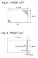
- An area sensor 60 with an imaging area of H pixels by V pixels is shown in Fig. 11, and a V-pixel long line sensor 61 which is driven in the direction of the arrow to subscan H pixels wide to image an area of H pixels by V pixels is shown in Fig. 12. If the per-pixel sensitivity of these sensors is equal, the line sensor requires an imaging time of H times that of the area sensor due to the charge storage time in order to achieve the same sensitivity. On the other hand, the line sensor has 1/H as many pixels as the area sensor, can therefore be achieved with a smaller sensor chip, and is thus used in image input devices having a large pixel count.
- US 5227888 discloses a still image pickup device including a moving two-dimensional sensor wherein the sensor forms an image of part of an image field and is then moved to a new position within the field, where another image of part of the image field is formed, until the sensor has covered the whole image field.
- an image moving continuously across an area sensor is obtained by a time-delay integration (TDI) operation.
- TDI time-delay integration
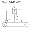
- Examples of devices using this TDI operation are disclosed in U.S. Patent No. 4,740,681, an apparatus for capturing images of stars that are moving due to the rotation of the imaging satellite, and U.S. Patent No. 4,922,337, an apparatus for capturing images of objects moving at a constant rate on a conveyor as shown in Fig. 13.
- a subject 38 on a conveyor 37 moving at a constant rate of speed is imaged by a camera 36 comprising a lens 35 and an area sensor 31.
- the area sensor 31 executes a TDI operation synchronized to the output of a tachometer 39 detecting the speed of the conveyor 37 to capture a still image of the subject 38.
- images are captured of subjects moving at a constant speed in a constant direction relative to a camera comprising a sensor that is in a fixed position relative to the lens.
- the object of the present invention is therefore to resolve the above-noted problems by providing a high resolution electronic camera that is capable of capturing images of common subjects from a hand-held position with an exposure time of less than one of several tenths of a second using a sensor chip that is sufficiently smaller than that of an area sensor.
- an electronic camera having a lens system for forming an image of the subject comprises a charge-. transfer type two-dimensional (X, Y) imaging device; a scanning means for subscanning the imaging device in the opposite-X direction and only in that direction, over the imaging plane of the lens system at a constant speed for at least the period from when the leading edge of the imaging device receptor enters the imaging area of the imaging plane until the trailing edge of the receptor leaves said imaging area with a subscanning time not greater than one tenth of a second; an X clock generator for transferring the photoelectric charges of the imaging device parallel to the X direction at the same speed as the subscanning operation; a Y clock generator for serially transferring in the Y direction the charge collected at the X end of the imaging device; and, an image signal circuit for processing the Y direction output of the imaging device.
- X, Y transfer type two-dimensional
- Fig. 1 is a basic overview of a electronic camera according to the invention.
- a charge-transfer type two-dimensional imaging device 2 is provided at the imaging plane of the lens system 1, and is driven in the direction of the arrow by the scanning device 4 fixed to camera chassis 3 to subscan the imaging plane 3a defined by an opening formed in the camera chassis.
- the scanning device 4 comprises a motor 43, linear slide mechanism 44, position detector 45, subscanning clock 41 and control circuit 42. A detail of the scanning device 4 will be described later in connection with Fig. 4.
- An X clock generator 5 supplies the X clock enabling TDI operation in parallel to the imaging device 2, and a Y clock generator 6 supplies a Y clock to the imaging device 2 causing the imaging device 2 to serially output the image signal.
- the image signal circuit 7 applies various common signal processing operations, such as amplification and compensation, to the image signal to generate the output signal of the camera.
- Fig. 2 shows the imaging device 2 and is used to describe the TDI operation thereof.
- the imaging device 2 comprises a receptor 20 comprising a V-row X register 22, a Y register 23 for serially outputting the signal charges collected in parallel at the X end of the X register 22, and an output circuit 24 for converting the collected signal charges to voltage values.
- Each X register 22 has P pixels aligned horizontally. There are V rows of X register 22.
- the receptor 20 includes P ⁇ V pixels.
- the subject image 21, such as letter "A" formed by the lens system 1 shown in Fig. 1 is still relative to the camera chassis 3, and is therefore moving in direction X as seen from the imaging device 2 when the imaging device 2 subscans in the opposite-X direction. Therefore, if X registers 22 are transferred in the opposite direction at the same speed as the movement, i.e., the subscanning, of the image 21, sensitivity corresponding to the pixel count P in the X direction is obtained as a result of TDI operation.
- the subscanning operation is shown in Fig. 3 in a cross section through the X axis.
- An H pixel wide image area 26 is defined on the imaging plane 25 of the lens system 1. This image area 26 corresponds to the effective output signal area of the camera.
- Position A at which the leading edge of the P pixel wide receptor 20 of the imaging device 2 meets the image area 26 is the imaging start position, and position B at which the trailing edge of the receptor 20 leaves the image area 26 is the imaging end position.
- the imaging device 2 subscans leftwardly in Fig. 3.
- the pixels in the first column will carry cumulated charges resulting from one unit time exposure.
- the imaging device 2 When the imaging device 2 is subscanned for another one pixel width distance, all the charges cumulated in the first column pixels are shifted or transferred in the scan direction X by one pixel width distance, i.e., to the second column pixels.
- the pixels in the first column will carry cumulated charges resulting from one unit time exposure
- the pixels in the second column will carry cumulated charges resulting from two unit time exposure.
- all the charges cumulated in the first and second column pixels are transferred in the scan direction X by one pixel width distance, i.e., respectively, to the second and third column pixels.
- the pixels in the first column will carry cumulated charges resulting from one unit time exposure
- the pixels in the second column will carry cumulated charges resulting from two unit time exposure
- the pixels in the third column will carry cumulated charges resulting from three unit time exposure.
- the pixels in the first column will carry cumulated charges resulting from one unit time exposure
- the pixels in the second column will carry cumulated charges resulting from two unit time exposure
- the pixels in the (P-1)th column will carry cumulated charges resulting from (P-1) unit time exposure
- the pixels in the Pth column will carry cumulated charges resulting from P unit time exposure.
- the charges in the Pth column representing the image data in the first column in the imaging plane 3a, are shifted to Y register 23, and all the remaining charges are transferred in the scan direction X by one pixel width distance. Since there will be no exposure being done in the Y register 23, the charges shifted to Y register 23 are resulted from P unit time exposure.
- the imaging device 2 is thus driven by the scanning device 4 at a constant speed D in the opposite-X direction to subscan the imaging plane 3a from at least position A to position B. Also, the imaging device 2 is driven by drive clocks produced from X clock generator 5 so that the charges are transferred at the same constant speed D in the X direction from one side of the imaging device 2 to the opposite side thereof.
- the imaging device 2 with a P pixel wide receptor compares favorably with the full area sensor having an H pixel wide receptor 60 such as shown in Fig. 11. Specifically, if the per-pixel sensitivity of both imaging devices 60 and 2 is the same, the per-pixel charge storage time will be the same and the same output signal voltage will be obtained if the sensor having an H pixel wide receptor subscans at a rate equal to (H+P)/P times the exposure time of the full area sensor.
- the characteristics of a electronic camera having a 1920 pixel (H) by 1080 pixel (V) image area are described below.
- the reference characteristics against which this electronic camera is compared are obtained from a 1/60 sec. /frame progressive scan HDTV camera that uses a full area sensor.
- the sensitivity of the imaging device 2 of the electronic camera is equal to the per-pixel sensitivity of the full area sensor of the HDTV camera.
- the receptor 20 of the electronic camera measures 384 pixels (H) by 1080 pixel (V), and the subscanning speed can be freely set.
- the maximum sensitivity of the HDTV camera is obtained when the charge storage time is 1/60 second.
- a 1/10 second shutter speed with a conventional silver halide film camera will produce noticeable image blurring due to hand movement during hand-held exposures.
- the subscanning time of the electronic camera of the present embodiment does not correspond to the lens shutter speed.
- the equivalent shutter speed, i.e., per-pixel exposure time (charge storage time), when the subscanning speed is 1/10 second is 1/60 second, a speed at which there is minimal blurring due to hand movement and which is fast enough for practical hand-held photography.
- the above operation applies when recording the darkest subjects that can be captured by a TV camera.
- the required charge storage time of the typical TV camera sensor decreases with the electronic shutter, which controls the charge storage time, operating at 1/120 second, 1/240 second, or faster.
- the subscanning time of the electronic camera of the invention also decreases to 1/20 second, 1/40 second, and faster. As the subscanning time decreases so do the effects of hand movement and subject movement.
- the electronic shutter of the imaging device 2 is used above the upper limit of the subscanning speed.
- the total pixel count of the imaging device 2 in the electronic camera of the present embodiment is approximately 410,000, or approximately 1/5 the pixel count of the above-noted full area sensor.
- the imaging device 2 can therefore be achieved with a smaller chip, the smaller chip area and resulting yield improvements combine to significantly reduce the cost of the imaging device, and it is therefore possible to construct a low cost, high resolution electronic camera.
- the scanning device 4 comprises a motor 43 that is synchronously driven by a control circuit 42 based on a subscanning clock 41, and a slide mechanism 44 having a support 8 on which the imaging device 2 is mounted.
- Motor 43 provides a driving power so that the imaging device 2 is transported in opposite-X direction at a constant speed D.
- the motor 43 may be a stepping motor or other motor that operates at a rotational or linear speed determined by the drive frequency, or a motor that is synchronously controlled by the control circuit 42.
- the subscanning speed D of the slide mechanism 44 is synchronized to the subscanning clock 41.
- the X drive clock for transferring the charges in the imaging device 2 in X direction at the speed D is generated by the X clock generator 5, which is also based on the subscanning clock 41.
- the subscanning speed D and the charge transfer speed D in the X register 22 of the imaging device 2 are controlled to the same speed, but in opposite direction.
- TDI operation can therefore be achieved.
- the scanning device 4 additionally comprises a position detector 45 for detecting the position of the imaging device 2 along the slide mechanism 44.
- the motor 43 is controlled by the control circuit 42 based on the subscanning clock 41 and referenced to the output from the position detector 45 to transport the scanning device 4 at a constant speed through the subscanning area.
- the X clock of the imaging device 2 is generated by the X clock generator 5 based on the output pulse from the position detector 45.
- the scanning device 4 of Fig. 4 since there is no position detector 45, the position of the imaging device 2 is controlled by the number of drive pulses supplied to the stepping motor 43. Thus, the scanning device 4 of Fig. 4 required a precise control of the drive pulse applied to the stepping motor, as well as the precise movement of the stepping motor.
- motor 43 can be a DC motor with the drive signal being a DC current. In this case the motor is not required to have a precise movement as the stepping motor.
- the charge transferring speed is also varied so as to keep charging the same location within the imaging plane 3a. In this manner stable TDI operation can be achieved even if there is a slight variation in the subscanning speed D.
- a block diagram of the X clock generator 5 and the Y clock generator 6 is shown.
- the four-phase X clocks ⁇ 1, ⁇ 2, ⁇ 3, ⁇ 4 supplied to the imaging device 2 is obtained by the X frequency divider 46 of the X clock generator 5.
- Four overlapping pulses of the four-phase X clocks ⁇ 1, ⁇ 2, ⁇ 3, ⁇ 4 are used to transfer or shift the charge in X direction by one pixel pitch.
- the X frequency divider 46 devices the frequency of the subscanning clock 41 or the output pulse from the position detector 45.
- the four phase X clocks ⁇ 1, ⁇ 2, ⁇ 3, ⁇ 4 are shown in Fig. 6B.
- the output pulse is frequency divided after multiplying by a multiplier circuit 47 which may have a PLL circuit.
- the position detection pitch is therefore an integral multiple of the electrode pitch or pixel pitch of the X register 22 of the imaging device 2.
- the Y clock generator 6 generates a two-phase Y clocks ⁇ 1 and ⁇ 2 by frequency dividing the system clock 48 using Y frequency divider 49 so that the Y register 23 transfers V pixels during the time the X register 22 of the imaging device 2 transfers one pixel.
- the Y clock generator 6 also outputs a pixel clock to the image signal circuit 7.
- the two-phase Y clocks ⁇ 1 and ⁇ 2 are also shown in Fig. 6B. Note that during one pulse repetition period t of the X clock, there are V pulses for transferring all the charges shifted to the Y register 23 to output circuit 24.
- the imaging device 2 is arranged to take black and white images. Next, an arrangement for obtaining color images is described.
- a color filter 50 having RGB (red, green and blue) color filter stripes is shown.
- the RGB color filter stripes are aligned with the X register 22 on the surface of the receptor 20 of the imaging device 2 shown in Fig. 2. Note that the same color filter is used for the pixels aligned horizontally along one X register 22.
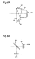
- Fig. 8A shows an optical color separation system in which color separation prisms are used instead of the color filter. More specifically, imaging devices 2R, 2B and 2G are fixed in position to the R-selective prism 51, B-selective prism 52, and G-transmitting prism 53, respectively. Each prism 51, 52, 53 has a size so as to cover, not the full imaging plane, but only the imaging device.
- the optical color separation system shown in Fig. 8A is formed integrally and mounted on the support 8, and subscans the image with the scanning device 4. Because the width of the imaging device 2 in the X direction is narrower than that of a conventional area sensor, smaller prisms can be used to achieve this color separation system, and the camera can therefore be built smaller.
- Fig. 8B shows another optical color separation system in which mirrors are used instead of the prisms. More specifically, a color separation mirror 54 reflects green light and has transparent characteristics with respect to red and blue lights. The reflected green lights are detected by imaging device 2G. The red and blue lights passed through the mirror 54 pass through red and blue stripe color filter 50 and are detected by imaging device 2RB.
- color imaging method of the invention can be achieved in various ways other than that described above depending upon the number of imaging devices used and the method of providing filters.
- FIG. 9 a modification of the electronic camera is shown.
- the electronic camera of the invention as shown in Fig. 1 is used connected to a video recording device in a manner similar to that of a conventional TV camera.
- the scanner-type electronic camera of the present embodiment as shown in Fig. 9, however, can be used as a stand-alone camera.
- This electronic camera is identical to that of the first embodiment in Fig. 1 from the lens system 1 to the image signal circuit 7.
- the electronic camera of Fig. 9 differs from the first embodiment of Fig. 1 in having an image memory 8 and display device 10 connected to the image signal circuit 7 with camera power supplied from a battery 9.
- the image memory 8 can store plural imaged pictures, and the display device 10 is used to present the image signal on a display for viewing.
- the image memory 8, battery 9, and display device 10 are built in to the camera to enable portable, stand-alone use of the electronic camera.
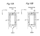
- the imaging device 2 of a electronic camera according to Fig. 10A or 10B comprises the X register 22 and Y register 23 of the imaging device 2 as shown in Fig. 2, and an additional Y register 27 on the side of the X register 22 opposite that of the first Y register 23.
- images are captured by means of bidirectional subscanning as shown in Figs. 10A and 10B.
- the subscanning operation in Fig. 10A is identical to the subscanning operation shown in Fig. 2. During this subscanning operation the output port is switched to Y register 23, and the output from the second Y register 27 is not used.
- the phase of the X clock supplied to the X register 22 is inverted, the charge transfer direction is reversed, and the output port is switched to obtain output from the second Y register 27. While the right and left sides of the image are reversed in the output signals obtained from the two Y registers 23 and 27, this right-left side inversion can be corrected by appropriately addressing the memory when storing the image signal.
- Constructing a electronic camera as described in connection with Figs. 10A and 10B achieves a scanner-type electronic camera that is capable of imaging in both scanning directions, and is advantageous with respect to improving the continuous imaging speed and reducing power consumption.
- the present invention provides an effective means of achieving a high resolution electronic camera enabling hand-held imaging of common, indeterminately moving subjects by means of low cost imaging devices having significantly fewer pixels than a common area sensor of comparable sensitivity.
Description
- The invention relates to a electronic camera for forming images by mechanically scanning an imaging device.
- Imaging methods used by conventional still-camera type image input devices include the common method using a two-dimensional imaging device (commonly called an "area sensor"), and methods whereby a two-dimensional image is obtained by mechanically scanning an image using a one-dimensional imaging device (commonly called a "line sensor") as disclosed in Japanese laid-open (tokkai) patent number H5-316302.
- An
area sensor 60 with an imaging area of H pixels by V pixels is shown in Fig. 11, and a V-pixellong line sensor 61 which is driven in the direction of the arrow to subscan H pixels wide to image an area of H pixels by V pixels is shown in Fig. 12. If the per-pixel sensitivity of these sensors is equal, the line sensor requires an imaging time of H times that of the area sensor due to the charge storage time in order to achieve the same sensitivity. On the other hand, the line sensor has 1/H as many pixels as the area sensor, can therefore be achieved with a smaller sensor chip, and is thus used in image input devices having a large pixel count. - US 5227888 discloses a still image pickup device including a moving two-dimensional sensor wherein the sensor forms an image of part of an image field and is then moved to a new position within the field, where another image of part of the image field is formed, until the sensor has covered the whole image field.
- In one specialized image input method an image moving continuously across an area sensor is obtained by a time-delay integration (TDI) operation. Examples of devices using this TDI operation are disclosed in U.S. Patent No. 4,740,681, an apparatus for capturing images of stars that are moving due to the rotation of the imaging satellite, and U.S. Patent No. 4,922,337, an apparatus for capturing images of objects moving at a constant rate on a conveyor as shown in Fig. 13.
- Referring to Fig. 13, a
subject 38 on aconveyor 37 moving at a constant rate of speed is imaged by acamera 36 comprising alens 35 and anarea sensor 31. Thearea sensor 31 executes a TDI operation synchronized to the output of atachometer 39 detecting the speed of theconveyor 37 to capture a still image of thesubject 38.
What is common to each of the above-described apparatuses is that images are captured of subjects moving at a constant speed in a constant direction relative to a camera comprising a sensor that is in a fixed position relative to the lens. There are no examples in the literature of methods using this TDI operation compatible with conventional cameras used to capture images of common, indeterminately-moving subjects. - Using an area sensor to construct a high resolution camera such as an HDTV camera having more than two-million pixels requires a large-scale chip, resulting in an extremely high cost. Camera-type scanners using a line sensor are widely available, but require a per-image scanning time of many seconds. As a result such scanners are limited to applications in which the camera is fixed on a stand and used to capture still subjects.
- The object of the present invention is therefore to resolve the above-noted problems by providing a high resolution electronic camera that is capable of capturing images of common subjects from a hand-held position with an exposure time of less than one of several tenths of a second using a sensor chip that is sufficiently smaller than that of an area sensor.
- To achieve this object an electronic camera having a lens system for forming an image of the subject comprises a charge-. transfer type two-dimensional (X, Y) imaging device; a scanning means for subscanning the imaging device in the opposite-X direction and only in that direction, over the imaging plane of the lens system at a constant speed for at least the period from when the leading edge of the imaging device receptor enters the imaging area of the imaging plane until the trailing edge of the receptor leaves said imaging area with a subscanning time not greater than one tenth of a second; an X clock generator for transferring the photoelectric charges of the imaging device parallel to the X direction at the same speed as the subscanning operation; a Y clock generator for serially transferring in the Y direction the charge collected at the X end of the imaging device; and, an image signal circuit for processing the Y direction output of the imaging device.
- The present invention will become more fully understood from the detailed description given below and the accompanying diagrams wherein:
- Fig. 1 is a basic configuration diagram of a still camera according to the invention.
- Fig. 2 is a diagram showing the imaging device of the invention and is used to describe the basic operation thereof.
- Fig. 3 is a diagram showing the basic subscanning operation of the invention.
- Fig. 4 is a diagram of a scanning device in one embodiment of the invention.
- Fig. 5 is a block diagram of a scanning device in another embodiment of the invention.
- Fig. 6A is a block diagram of the clock generator in one embodiment of the invention.
- Fig. 6B is a wave form showing X clock and Y clock.
- Fig. 7 is a diagram showing the color filter used in one embodiment of the invention.
- Fig. 8A is a diagram showing color separation prisms used in one embodiment of the invention.
- Fig. 8B is a diagram showing color separation mirror used in another embodiment of the invention.
- Fig. 9 is a basic configuration diagram of a still camera according to another embodiment of the invention.
- Figs. 10A and 10B are diagrams showing the bidirectional subscanning operation of an alternative embodiment of the invention.
- Fig. 11 is a diagram showing a conventional area sensor.
- Fig. 12 is a diagram showing the two-dimensional imaging operation using a conventional line sensor.
- Fig. 13 is a diagram showing the configuration of a conventional apparatus using a TDI operation.
-
- The preferred embodiments of the present invention are described below with reference to the accompanying Fig. 1 to Fig. 10.
- Fig. 1 is a basic overview of a electronic camera according to the invention. As shown in Fig. 1, a charge-transfer type two-
dimensional imaging device 2 is provided at the imaging plane of thelens system 1, and is driven in the direction of the arrow by thescanning device 4 fixed tocamera chassis 3 to subscan theimaging plane 3a defined by an opening formed in the camera chassis. Theimaging plane 3a has a size capable of covering H pixels aligned horizontally and V pixels aligned vertically. According to the preferred embodiment, H=1920 and V=1080. - The
scanning device 4 comprises amotor 43,linear slide mechanism 44,position detector 45,subscanning clock 41 andcontrol circuit 42. A detail of thescanning device 4 will be described later in connection with Fig. 4. - An
X clock generator 5 supplies the X clock enabling TDI operation in parallel to theimaging device 2, and aY clock generator 6 supplies a Y clock to theimaging device 2 causing theimaging device 2 to serially output the image signal. Theimage signal circuit 7 applies various common signal processing operations, such as amplification and compensation, to the image signal to generate the output signal of the camera. - Fig. 2 shows the
imaging device 2 and is used to describe the TDI operation thereof. As shown in Fig. 2 theimaging device 2 comprises areceptor 20 comprising a V-row X register 22, aY register 23 for serially outputting the signal charges collected in parallel at the X end of theX register 22, and anoutput circuit 24 for converting the collected signal charges to voltage values. EachX register 22 has P pixels aligned horizontally. There are V rows ofX register 22. Thus, thereceptor 20 includes P × V pixels. According to one preferred embodiment, P=384 and V=1080. From a different viewpoint, it can be said that there are P columns of pixels, each column including V pixels aligned vertically. The number of pixels aligned vertically in theY register 23 is also V. Photoelectric conversion is accomplished by theX register 22, and the elements other than thereceptor 20 are shielded from light. - The
subject image 21, such as letter "A" formed by thelens system 1 shown in Fig. 1 is still relative to thecamera chassis 3, and is therefore moving in direction X as seen from theimaging device 2 when theimaging device 2 subscans in the opposite-X direction. Therefore, ifX registers 22 are transferred in the opposite direction at the same speed as the movement, i.e., the subscanning, of theimage 21, sensitivity corresponding to the pixel count P in the X direction is obtained as a result of TDI operation. - The subscanning operation is shown in Fig. 3 in a cross section through the X axis. An H pixel
wide image area 26 is defined on theimaging plane 25 of thelens system 1. Thisimage area 26 corresponds to the effective output signal area of the camera. Position A at which the leading edge of the P pixelwide receptor 20 of theimaging device 2 meets theimage area 26 is the imaging start position, and position B at which the trailing edge of thereceptor 20 leaves theimage area 26 is the imaging end position. - Starting from position A, the
imaging device 2 subscans leftwardly in Fig. 3. - When the
imaging device 2 is subscanned for one pixel width distance, the pixels in the first column will carry cumulated charges resulting from one unit time exposure. - When the
imaging device 2 is subscanned for another one pixel width distance, all the charges cumulated in the first column pixels are shifted or transferred in the scan direction X by one pixel width distance, i.e., to the second column pixels. The pixels in the first column will carry cumulated charges resulting from one unit time exposure, and the pixels in the second column will carry cumulated charges resulting from two unit time exposure. - When the
imaging device 2 is subscanned for yet another one pixel width distance (i.e., three pixel width distance from the start), all the charges cumulated in the first and second column pixels are transferred in the scan direction X by one pixel width distance, i.e., respectively, to the second and third column pixels. The pixels in the first column will carry cumulated charges resulting from one unit time exposure, the pixels in the second column will carry cumulated charges resulting from two unit time exposure, and the pixels in the third column will carry cumulated charges resulting from three unit time exposure. - In this manner, when the
imaging device 2 is subscanned for P pixel width distance from the start, the charges in the (P-1)th column are transferred to the Pth column, those in the (P-2)th column are transferred to the (P-1)th column, those in the (P-3)th column are transferred to the (P-3)th column, and so on. Thus, the pixels in the first column will carry cumulated charges resulting from one unit time exposure, the pixels in the second column will carry cumulated charges resulting from two unit time exposure, ..., the pixels in the (P-1)th column will carry cumulated charges resulting from (P-1) unit time exposure, and the pixels in the Pth column will carry cumulated charges resulting from P unit time exposure. - Then, when the
imaging device 2 is subscanned for (P+1) pixel width distance from the start, the charges in the Pth column, representing the image data in the first column in theimaging plane 3a, are shifted to Y register 23, and all the remaining charges are transferred in the scan direction X by one pixel width distance. Since there will be no exposure being done in theY register 23, the charges shifted to Y register 23 are resulted from P unit time exposure. - Thereafter, when the
imaging device 2 is subscanned for (H+P) pixel width distance from the start, i.e., to the position B shown in Fig. 3, the charges in the Pth column, representing the image data of the last column in theimaging plane 3a, are shifted to Y register 23. - As will be explained in detail later, since the subscanning speed of the
imaging device 2 in the opposite-X direction, and the transferring speed of the charges in the X direction are the same, the charges are being cumulated in the same positional column within theimaging plane 3a with the same exposure time (P unit time). - The
imaging device 2 is thus driven by thescanning device 4 at a constant speed D in the opposite-X direction to subscan theimaging plane 3a from at least position A to position B. Also, theimaging device 2 is driven by drive clocks produced fromX clock generator 5 so that the charges are transferred at the same constant speed D in the X direction from one side of theimaging device 2 to the opposite side thereof. - The
imaging device 2 with a P pixel wide receptor compares favorably with the full area sensor having an H pixelwide receptor 60 such as shown in Fig. 11. Specifically, if the per-pixel sensitivity of bothimaging devices - The characteristics of a electronic camera having a 1920 pixel (H) by 1080 pixel (V) image area are described below. The reference characteristics against which this electronic camera is compared are obtained from a 1/60 sec. /frame progressive scan HDTV camera that uses a full area sensor. The sensitivity of the
imaging device 2 of the electronic camera is equal to the per-pixel sensitivity of the full area sensor of the HDTV camera. Thereceptor 20 of the electronic camera measures 384 pixels (H) by 1080 pixel (V), and the subscanning speed can be freely set. The maximum sensitivity of the HDTV camera is obtained when the charge storage time is 1/60 second. Based on the above equation (H+P)/P and the widths of H=1920 and P=384, (H+P)/P=6 is obtained. Thus, theexposure time 1/60 second using the fullarea imaging device 60 is comparable to theexposure time 1/10 second (= 1/60 × 6) using theimaging device 2. - It should be noted that a 1/10 second shutter speed with a conventional silver halide film camera will produce noticeable image blurring due to hand movement during hand-held exposures. However, the subscanning time of the electronic camera of the present embodiment does not correspond to the lens shutter speed. The equivalent shutter speed, i.e., per-pixel exposure time (charge storage time), when the subscanning speed is 1/10 second is 1/60 second, a speed at which there is minimal blurring due to hand movement and which is fast enough for practical hand-held photography.
- Blurring due to subject movement during the subscanning time is also relative to the exposure time and is therefore not a particular problem.
- It should also be noted that the above operation applies when recording the darkest subjects that can be captured by a TV camera. As the subject brightness increases the required charge storage time of the typical TV camera sensor decreases with the electronic shutter, which controls the charge storage time, operating at 1/120 second, 1/240 second, or faster. This means that the subscanning time of the electronic camera of the invention also decreases to 1/20 second, 1/40 second, and faster. As the subscanning time decreases so do the effects of hand movement and subject movement. The electronic shutter of the
imaging device 2 is used above the upper limit of the subscanning speed. - The total pixel count of the
imaging device 2 in the electronic camera of the present embodiment is approximately 410,000, or approximately 1/5 the pixel count of the above-noted full area sensor. Theimaging device 2 can therefore be achieved with a smaller chip, the smaller chip area and resulting yield improvements combine to significantly reduce the cost of the imaging device, and it is therefore possible to construct a low cost, high resolution electronic camera. - Referring to Fig. 4, a block diagram of a
scanning device 4 using a synchronous motor is shown. Thescanning device 4 comprises amotor 43 that is synchronously driven by acontrol circuit 42 based on asubscanning clock 41, and aslide mechanism 44 having asupport 8 on which theimaging device 2 is mounted.Motor 43 provides a driving power so that theimaging device 2 is transported in opposite-X direction at a constant speed D. - The
motor 43 may be a stepping motor or other motor that operates at a rotational or linear speed determined by the drive frequency, or a motor that is synchronously controlled by thecontrol circuit 42. Thus, theimaging device 2 is moved in the opposite-X direction at the subscanning speed D. The subscanning speed D of theslide mechanism 44 is synchronized to thesubscanning clock 41. The X drive clock for transferring the charges in theimaging device 2 in X direction at the speed D is generated by theX clock generator 5, which is also based on thesubscanning clock 41. As a result the subscanning speed D and the charge transfer speed D in theX register 22 of theimaging device 2 are controlled to the same speed, but in opposite direction. Thus, TDI operation can therefore be achieved. - Referring to Fig. 5, a modification of a
scanning device 4 is shown. Thescanning device 4 additionally comprises aposition detector 45 for detecting the position of theimaging device 2 along theslide mechanism 44. Themotor 43 is controlled by thecontrol circuit 42 based on thesubscanning clock 41 and referenced to the output from theposition detector 45 to transport thescanning device 4 at a constant speed through the subscanning area. The X clock of theimaging device 2 is generated by theX clock generator 5 based on the output pulse from theposition detector 45. As a result, the subscanning speed D and the transfer speed D of theX register 22 of theimaging device 2 can be controlled to the same speed, and stable TDI operation can be achieved even if there is a slight variation in the subscanning speed. - According to the
scanning device 4 of Fig. 4, since there is noposition detector 45, the position of theimaging device 2 is controlled by the number of drive pulses supplied to the steppingmotor 43. Thus, thescanning device 4 of Fig. 4 required a precise control of the drive pulse applied to the stepping motor, as well as the precise movement of the stepping motor. - However, according to the
scanning device 4 of Fig. 5, sinceposition detector 45 is provided,motor 43 can be a DC motor with the drive signal being a DC current. In this case the motor is not required to have a precise movement as the stepping motor. When the motor speed should vary, as detected by thecontrol circuit 42, the charge transferring speed is also varied so as to keep charging the same location within theimaging plane 3a. In this manner stable TDI operation can be achieved even if there is a slight variation in the subscanning speed D. - Referring to Fig. 6A, a block diagram of the
X clock generator 5 and theY clock generator 6 is shown. The four-phase X clocks 1, 2, 3, 4 supplied to theimaging device 2 is obtained by theX frequency divider 46 of theX clock generator 5. Four overlapping pulses of the four-phase X clocks 1, 2, 3, 4 are used to transfer or shift the charge in X direction by one pixel pitch. TheX frequency divider 46 devices the frequency of thesubscanning clock 41 or the output pulse from theposition detector 45. - The four phase X clocks 1, 2, 3, 4 are shown in Fig. 6B. When the electrode pitch or pixel pitch of the
X register 22 of theimaging device 2 is R (meter) and the subscanning speed is D (meter/sec), the pulse repetition period t (sec) can be given by t = R/D. According to one embodiment, R=10 (µm) and D=1 (meter/sec), t=10 (µs). - If the position detection pitch of the
position detector 45 is coarser than the electrode pitch or pixel pitch of theX register 22 of theimaging device 2, the output pulse is frequency divided after multiplying by amultiplier circuit 47 which may have a PLL circuit. The position detection pitch is therefore an integral multiple of the electrode pitch or pixel pitch of theX register 22 of theimaging device 2. - The
Y clock generator 6 generates a two-phase Y clocks 1 and 2 by frequency dividing thesystem clock 48 usingY frequency divider 49 so that theY register 23 transfers V pixels during the time theX register 22 of theimaging device 2 transfers one pixel. TheY clock generator 6 also outputs a pixel clock to theimage signal circuit 7. - The two-phase Y clocks 1 and 2 are also shown in Fig. 6B. Note that during one pulse repetition period t of the X clock, there are V pulses for transferring all the charges shifted to the
Y register 23 tooutput circuit 24. - In the above embodiment, the
imaging device 2 is arranged to take black and white images. Next, an arrangement for obtaining color images is described. - Referring to Fig. 7, a
color filter 50 having RGB (red, green and blue) color filter stripes is shown. The RGB color filter stripes are aligned with theX register 22 on the surface of thereceptor 20 of theimaging device 2 shown in Fig. 2. Note that the same color filter is used for the pixels aligned horizontally along oneX register 22. By time-series processing the output from thecolor filter 50, the color signals obtained by TDI operation can be separated, thereby achieving a color image. - Fig. 8A shows an optical color separation system in which color separation prisms are used instead of the color filter. More specifically,
imaging devices selective prism 51, B-selective prism 52, and G-transmitting prism 53, respectively. Eachprism support 8, and subscans the image with thescanning device 4. Because the width of theimaging device 2 in the X direction is narrower than that of a conventional area sensor, smaller prisms can be used to achieve this color separation system, and the camera can therefore be built smaller. - Fig. 8B shows another optical color separation system in which mirrors are used instead of the prisms. More specifically, a
color separation mirror 54 reflects green light and has transparent characteristics with respect to red and blue lights. The reflected green lights are detected byimaging device 2G. The red and blue lights passed through themirror 54 pass through red and bluestripe color filter 50 and are detected by imaging device 2RB. - It should be noted that the color imaging method of the invention can be achieved in various ways other than that described above depending upon the number of imaging devices used and the method of providing filters.
- Referring to Fig. 9, a modification of the electronic camera is shown. The electronic camera of the invention as shown in Fig. 1 is used connected to a video recording device in a manner similar to that of a conventional TV camera. The scanner-type electronic camera of the present embodiment as shown in Fig. 9, however, can be used as a stand-alone camera. This electronic camera is identical to that of the first embodiment in Fig. 1 from the
lens system 1 to theimage signal circuit 7. - The electronic camera of Fig. 9 differs from the first embodiment of Fig. 1 in having an
image memory 8 anddisplay device 10 connected to theimage signal circuit 7 with camera power supplied from abattery 9. Theimage memory 8 can store plural imaged pictures, and thedisplay device 10 is used to present the image signal on a display for viewing. Theimage memory 8,battery 9, anddisplay device 10 are built in to the camera to enable portable, stand-alone use of the electronic camera. - Conventional camera-type scanners using a line sensor require a long exposure time as previously explained, must therefore be used in a stationary position, and are thus not practical for use as a portable, stand-alone electronic camera. The ability to provide such a portable, stand-alone electronic camera is a major advantage of the present invention.
- Referring to Figs. 10A and 10B, a modification of the imaging device is shown. The
imaging device 2 of a electronic camera according to Fig. 10A or 10B comprises theX register 22 and Y register 23 of theimaging device 2 as shown in Fig. 2, and anadditional Y register 27 on the side of theX register 22 opposite that of thefirst Y register 23. Thus configured, images are captured by means of bidirectional subscanning as shown in Figs. 10A and 10B. - The subscanning operation in Fig. 10A is identical to the subscanning operation shown in Fig. 2. During this subscanning operation the output port is switched to Y register 23, and the output from the
second Y register 27 is not used. When subscanning in the opposite direction as shown in Fig. 10B, the phase of the X clock supplied to theX register 22 is inverted, the charge transfer direction is reversed, and the output port is switched to obtain output from thesecond Y register 27. While the right and left sides of the image are reversed in the output signals obtained from the two Y registers 23 and 27, this right-left side inversion can be corrected by appropriately addressing the memory when storing the image signal. - Constructing a electronic camera as described in connection with Figs. 10A and 10B achieves a scanner-type electronic camera that is capable of imaging in both scanning directions, and is advantageous with respect to improving the continuous imaging speed and reducing power consumption.
- It should be noted that all references to the two-dimensional axes X and Y in the above disclosure have been used for the convenience of explanation only. The directions of these axes are relative to each other, and the invention shall not be limited thereby.
- As will be known from the preceding descriptions of the embodiments, the present invention provides an effective means of achieving a high resolution electronic camera enabling hand-held imaging of common, indeterminately moving subjects by means of low cost imaging devices having significantly fewer pixels than a common area sensor of comparable sensitivity.
Claims (11)
- An electronic camera having a lens system for forming an image of the subject comprising:a charge-transfer type two-dimensional (X, Y) imaging device (2);a scanning means (4) for subscanning the imaging device in the opposite-X direction, and only in that direction, over the imaging plane of the lens system at a constant speed for at least the period from when the leading edge of the imaging device receptor enters the imaging area of the imaging plane until the trailing edge of the receptor leaves said imaging area with a subscanning time not greater than one tenth of a second;an X clock generator (5) for transferring the photoelectric charges of the imaging device parallel to the X direction at the same speed as the subscanning operation;a Y clock generator (6) for serially transferring in the Y direction the charge collected at the X end of the imaging device; and,an image signal circuit (7) for processing the Y-direction output of the imaging device.
- The electronic camera according to claim 1 wherein the scanning means comprises a motor (43) that operates synchronized to the subscanning clock, and the X clock is generated from the subscanning clock.
- The electronic camera according to claim 1 wherein the scanning means comprises a position detector (45) for detecting the scanning position of the imaging device, and the X clock is generated synchronized to the output pulse of the position detector.
- The electronic camera according to claim 3 wherein the scanning means comprises a motor (43) that is controlled according to the output pulse of the position detector.
- The electronic camera according to claim 3 or 4, wherein the position detection pitch of the position detector (45) is an integral multiple of the X-direction pixel pitch of the imaging device.
- The electronic camera according to any one of the preceding claims wherein striped color filters (50) of the same color are disposed in the X direction on the surface of the imaging device.
- The electronic camera according to any one of claims 1 to 5, wherein color separation prisms (51,52) are disposed in front of the plural imaging devices, and said color separation prisms subscan integrally with the imaging devices.
- The electronic camera according to any one of claims 1 to 5, wherein color separation mirrors (54) are disposed in front of the plural imaging devices, and said color separation mirrors subscan integrally with the imaging devices.
- The electronic camera according to any one of the preceding claims wherein a power supply battery (9) and image memory (8) with a plural image storage capacity are built in to the camera.
- The electronic camera according to any one of the preceding claims wherein a display device (10) for displaying the recorded image signal is built in to the camera.
- The electronic camera according to any one of the preceding claims, further comprising a further Y-direction charge-transfer register (27) disposed to the opposite-X direction of the imaging device, and enabling bidirectional imaging by switching the X-direction charge transfer direction and the subscanning direction of the scanning means.
Applications Claiming Priority (3)
| Application Number | Priority Date | Filing Date | Title |
|---|---|---|---|
| JP8052771A JPH09247545A (en) | 1996-03-11 | 1996-03-11 | Scanner type electronic camera |
| JP52771/96 | 1996-03-11 | ||
| JP5277196 | 1996-03-11 |
Publications (3)
| Publication Number | Publication Date |
|---|---|
| EP0796005A2 EP0796005A2 (en) | 1997-09-17 |
| EP0796005A3 EP0796005A3 (en) | 1998-08-12 |
| EP0796005B1 true EP0796005B1 (en) | 2004-09-29 |
Family
ID=12924139
Family Applications (1)
| Application Number | Title | Priority Date | Filing Date |
|---|---|---|---|
| EP97301517A Expired - Lifetime EP0796005B1 (en) | 1996-03-11 | 1997-03-06 | Electronic camera using a small sensor with high speed imaging |
Country Status (4)
| Country | Link |
|---|---|
| US (1) | US6005617A (en) |
| EP (1) | EP0796005B1 (en) |
| JP (1) | JPH09247545A (en) |
| DE (1) | DE69730890T2 (en) |
Cited By (3)
| Publication number | Priority date | Publication date | Assignee | Title |
|---|---|---|---|---|
| US8755579B2 (en) | 2000-05-03 | 2014-06-17 | Leica Biosystems Imaging, Inc. | Fully automatic rapid microscope slide scanner |
| US8805050B2 (en) | 2000-05-03 | 2014-08-12 | Leica Biosystems Imaging, Inc. | Optimizing virtual slide image quality |
| US9235041B2 (en) | 2005-07-01 | 2016-01-12 | Leica Biosystems Imaging, Inc. | System and method for single optical axis multi-detector microscope slide scanner |
Families Citing this family (39)
| Publication number | Priority date | Publication date | Assignee | Title |
|---|---|---|---|---|
| US6847729B1 (en) | 1999-04-21 | 2005-01-25 | Fairfield Imaging Limited | Microscopy |
| US7518652B2 (en) | 2000-05-03 | 2009-04-14 | Aperio Technologies, Inc. | Method and apparatus for pre-focus in a linear array based slide scanner |
| US7738688B2 (en) | 2000-05-03 | 2010-06-15 | Aperio Technologies, Inc. | System and method for viewing virtual slides |
| TW526660B (en) * | 2000-08-07 | 2003-04-01 | Matsushita Electric Ind Co Ltd | Device and method for reading image, and recording medium for image reading program |
| US7907765B2 (en) | 2001-03-28 | 2011-03-15 | University Of Washington | Focal plane tracking for optical microtomography |
| US20060023219A1 (en) * | 2001-03-28 | 2006-02-02 | Meyer Michael G | Optical tomography of small objects using parallel ray illumination and post-specimen optical magnification |
| US6944322B2 (en) | 2001-03-28 | 2005-09-13 | Visiongate, Inc. | Optical tomography of small objects using parallel ray illumination and post-specimen optical magnification |
| US6591003B2 (en) * | 2001-03-28 | 2003-07-08 | Visiongate, Inc. | Optical tomography of small moving objects using time delay and integration imaging |
| US7009163B2 (en) | 2001-06-22 | 2006-03-07 | Orbotech Ltd. | High-sensitivity optical scanning using memory integration |
| JP2003046862A (en) | 2001-08-01 | 2003-02-14 | Hamamatsu Photonics Kk | X-ray image pickup device |
| US6741730B2 (en) | 2001-08-10 | 2004-05-25 | Visiongate, Inc. | Method and apparatus for three-dimensional imaging in the fourier domain |
| SE523681C2 (en) * | 2002-04-05 | 2004-05-11 | Integrated Vision Prod | System and sensor for mapping properties of an object |
| US7811825B2 (en) * | 2002-04-19 | 2010-10-12 | University Of Washington | System and method for processing specimens and images for optical tomography |
| US7260253B2 (en) | 2002-04-19 | 2007-08-21 | Visiongate, Inc. | Method for correction of relative object-detector motion between successive views |
| US20050085708A1 (en) * | 2002-04-19 | 2005-04-21 | University Of Washington | System and method for preparation of cells for 3D image acquisition |
| US7738945B2 (en) * | 2002-04-19 | 2010-06-15 | University Of Washington | Method and apparatus for pseudo-projection formation for optical tomography |
| US7197355B2 (en) | 2002-04-19 | 2007-03-27 | Visiongate, Inc. | Variable-motion optical tomography of small objects |
| US6697508B2 (en) | 2002-05-10 | 2004-02-24 | Visiongate, Inc. | Tomographic reconstruction of small objects using a priori knowledge |
| US6770893B2 (en) * | 2002-05-13 | 2004-08-03 | Visiongate, Inc. | Method and apparatus for emission computed tomography using temporal signatures |
| US6782334B1 (en) | 2003-04-01 | 2004-08-24 | Lockheed Martin Corporation | Method and system for calibration of time delay integration imaging devices |
| US7687167B2 (en) * | 2003-07-18 | 2010-03-30 | Panasonic Corporation | Power supply unit |
| JP2005197922A (en) * | 2004-01-06 | 2005-07-21 | Fuji Xerox Co Ltd | Image reading apparatus |
| DE102004007911B3 (en) * | 2004-02-13 | 2005-02-03 | Deutsches Zentrum für Luft- und Raumfahrt e.V. | Digital scanning device for color original using TDI-sensor and white light source with associated color liquid display matrix for providing successive red, green and blue light strips |
| JP5134365B2 (en) | 2004-05-27 | 2013-01-30 | アペリオ・テクノロジーズ・インコーポレイテッド | System and method for generating and visualizing a three-dimensional virtual slide |
| US6991738B1 (en) | 2004-10-13 | 2006-01-31 | University Of Washington | Flow-through drum centrifuge |
| US20060096358A1 (en) * | 2004-10-28 | 2006-05-11 | University Of Washington | Optical projection tomography microscope |
| US7494809B2 (en) * | 2004-11-09 | 2009-02-24 | Visiongate, Inc. | Automated cell sample enrichment preparation method |
| US20100066850A1 (en) * | 2006-11-30 | 2010-03-18 | Westar Display Technologies, Inc. | Motion artifact measurement for display devices |
| US7835561B2 (en) | 2007-05-18 | 2010-11-16 | Visiongate, Inc. | Method for image processing and reconstruction of images for optical tomography |
| JP4602380B2 (en) * | 2007-07-25 | 2010-12-22 | アドバンスド・マスク・インスペクション・テクノロジー株式会社 | Image input method using storage type sensor and apparatus therefor |
| US7787112B2 (en) * | 2007-10-22 | 2010-08-31 | Visiongate, Inc. | Depth of field extension for optical tomography |
| JP4968227B2 (en) * | 2008-10-03 | 2012-07-04 | 三菱電機株式会社 | Image sensor and driving method thereof |
| WO2010048584A2 (en) | 2008-10-24 | 2010-04-29 | Aperio Technologies, Inc. | Whole slide fluorescence scanner |
| US8254023B2 (en) | 2009-02-23 | 2012-08-28 | Visiongate, Inc. | Optical tomography system with high-speed scanner |
| US8964088B2 (en) | 2011-09-28 | 2015-02-24 | Semiconductor Components Industries, Llc | Time-delay-and-integrate image sensors having variable intergration times |
| JP5941659B2 (en) * | 2011-11-02 | 2016-06-29 | 浜松ホトニクス株式会社 | Solid-state imaging device |
| FR3002715B1 (en) * | 2013-02-28 | 2016-06-03 | E2V Semiconductors | METHOD FOR PRODUCING IMAGES AND LINEAR SENSOR CAMERA |
| US11069054B2 (en) | 2015-12-30 | 2021-07-20 | Visiongate, Inc. | System and method for automated detection and monitoring of dysplasia and administration of immunotherapy and chemotherapy |
| RU2706008C1 (en) * | 2019-03-12 | 2019-11-13 | Вячеслав Михайлович Смелков | Computer system for panoramic scanning of a monochrome image |
Family Cites Families (10)
| Publication number | Priority date | Publication date | Assignee | Title |
|---|---|---|---|---|
| JPS5455324A (en) * | 1977-10-13 | 1979-05-02 | Sony Corp | Color pickup unit |
| US4280141A (en) * | 1978-09-22 | 1981-07-21 | Mccann David H | Time delay and integration detectors using charge transfer devices |
| JPS6157176A (en) * | 1984-08-29 | 1986-03-24 | Dainippon Screen Mfg Co Ltd | Magnification variable control method |
| US4882619A (en) * | 1986-04-07 | 1989-11-21 | Olympus Optical Co., Ltd. | High resolution image pickup system with color dispersion means |
| JPH07105872B2 (en) * | 1987-04-30 | 1995-11-13 | 株式会社日立製作所 | Electronic filing device |
| JP2753541B2 (en) * | 1990-02-19 | 1998-05-20 | 株式会社ニコン | Still image pickup device |
| US5454102A (en) * | 1993-01-19 | 1995-09-26 | Canon Information Systems, Inc. | Method and apparatus for transferring structured data using a self-generating node network |
| JP3262441B2 (en) * | 1994-02-04 | 2002-03-04 | キヤノン株式会社 | Linear image sensor and image reading device |
| US5481300A (en) * | 1994-04-29 | 1996-01-02 | Motta; Ricardo J. | Image capture system |
| JPH09116818A (en) * | 1995-10-17 | 1997-05-02 | Purotetsuku Japan Kk | Image pickup circuit |
-
1996
- 1996-03-11 JP JP8052771A patent/JPH09247545A/en active Pending
-
1997
- 1997-03-06 DE DE69730890T patent/DE69730890T2/en not_active Expired - Fee Related
- 1997-03-06 EP EP97301517A patent/EP0796005B1/en not_active Expired - Lifetime
- 1997-03-10 US US08/813,188 patent/US6005617A/en not_active Expired - Fee Related
Cited By (5)
| Publication number | Priority date | Publication date | Assignee | Title |
|---|---|---|---|---|
| US8755579B2 (en) | 2000-05-03 | 2014-06-17 | Leica Biosystems Imaging, Inc. | Fully automatic rapid microscope slide scanner |
| US8805050B2 (en) | 2000-05-03 | 2014-08-12 | Leica Biosystems Imaging, Inc. | Optimizing virtual slide image quality |
| US9386211B2 (en) | 2000-05-03 | 2016-07-05 | Leica Biosystems Imaging, Inc. | Fully automatic rapid microscope slide scanner |
| US9535243B2 (en) | 2000-05-03 | 2017-01-03 | Leica Biosystems Imaging, Inc. | Optimizing virtual slide image quality |
| US9235041B2 (en) | 2005-07-01 | 2016-01-12 | Leica Biosystems Imaging, Inc. | System and method for single optical axis multi-detector microscope slide scanner |
Also Published As
| Publication number | Publication date |
|---|---|
| JPH09247545A (en) | 1997-09-19 |
| DE69730890T2 (en) | 2006-02-23 |
| EP0796005A2 (en) | 1997-09-17 |
| EP0796005A3 (en) | 1998-08-12 |
| DE69730890D1 (en) | 2004-11-04 |
| US6005617A (en) | 1999-12-21 |
Similar Documents
| Publication | Publication Date | Title |
|---|---|---|
| EP0796005B1 (en) | Electronic camera using a small sensor with high speed imaging | |
| US5650813A (en) | Panoramic time delay and integration video camera system | |
| JP3604480B2 (en) | Electronic camera with two modes for still image composition and recording | |
| JP3000308B2 (en) | Video camera | |
| EP0599470B1 (en) | Panoramic camera systems | |
| JP2753541B2 (en) | Still image pickup device | |
| JPH03502755A (en) | Photoelectric color image sensor | |
| JPH01280977A (en) | Method and apparatus for displaying slave picture of television system | |
| WO1999021354A1 (en) | System and method for image motion compensation of a ccd image sensor | |
| TWI242365B (en) | Solid photographing element and digital camera | |
| EP0082406B1 (en) | Focal zoom device | |
| JPH09172645A (en) | Electronic image sensor for color snapshot camera | |
| US5936668A (en) | Color image display device | |
| JPH1169209A (en) | Image-pickup device | |
| US5138454A (en) | Megapixel video previewer framestore and display | |
| US4151560A (en) | Apparatus and method for displaying moving film on a television receiver | |
| US6118481A (en) | Solid state image pick-up device and image pick-up apparatus | |
| US5497195A (en) | Electronic color snapshot technique and structure using very high resolution monochrome full frame CCD imagers | |
| JPH08242410A (en) | Electronic camera that creates interlaced image from sequential scanning sensor of electronic camera | |
| GB2162019A (en) | Compensating for camera movement | |
| JPH07240870A (en) | Image pickup device | |
| JP2002287197A (en) | Image stabilizing device for image pickup device | |
| JP4110236B2 (en) | CCD imaging device, driving method thereof, and film scanner | |
| US20020063869A1 (en) | Image display apparatus or image printing apparatus | |
| JPH0377483A (en) | Picture blur preventing camera |
Legal Events
| Date | Code | Title | Description |
|---|---|---|---|
| PUAI | Public reference made under article 153(3) epc to a published international application that has entered the european phase |
Free format text: ORIGINAL CODE: 0009012 |
|
| 17P | Request for examination filed |
Effective date: 19970327 |
|
| AK | Designated contracting states |
Kind code of ref document: A2 Designated state(s): DE FR GB |
|
| PUAL | Search report despatched |
Free format text: ORIGINAL CODE: 0009013 |
|
| AK | Designated contracting states |
Kind code of ref document: A3 Designated state(s): DE FR GB |
|
| 17Q | First examination report despatched |
Effective date: 20021210 |
|
| GRAP | Despatch of communication of intention to grant a patent |
Free format text: ORIGINAL CODE: EPIDOSNIGR1 |
|
| GRAS | Grant fee paid |
Free format text: ORIGINAL CODE: EPIDOSNIGR3 |
|
| GRAA | (expected) grant |
Free format text: ORIGINAL CODE: 0009210 |
|
| AK | Designated contracting states |
Kind code of ref document: B1 Designated state(s): DE FR GB |
|
| REG | Reference to a national code |
Ref country code: GB Ref legal event code: FG4D |
|
| REF | Corresponds to: |
Ref document number: 69730890 Country of ref document: DE Date of ref document: 20041104 Kind code of ref document: P |
|
| ET | Fr: translation filed | ||
| PLBE | No opposition filed within time limit |
Free format text: ORIGINAL CODE: 0009261 |
|
| STAA | Information on the status of an ep patent application or granted ep patent |
Free format text: STATUS: NO OPPOSITION FILED WITHIN TIME LIMIT |
|
| 26N | No opposition filed |
Effective date: 20050630 |
|
| PGFP | Annual fee paid to national office [announced via postgrant information from national office to epo] |
Ref country code: GB Payment date: 20090304 Year of fee payment: 13 |
|
| PGFP | Annual fee paid to national office [announced via postgrant information from national office to epo] |
Ref country code: DE Payment date: 20090226 Year of fee payment: 13 |
|
| PGFP | Annual fee paid to national office [announced via postgrant information from national office to epo] |
Ref country code: FR Payment date: 20090316 Year of fee payment: 13 |
|
| GBPC | Gb: european patent ceased through non-payment of renewal fee |
Effective date: 20100306 |
|
| REG | Reference to a national code |
Ref country code: FR Ref legal event code: ST Effective date: 20101130 |
|
| PG25 | Lapsed in a contracting state [announced via postgrant information from national office to epo] |
Ref country code: FR Free format text: LAPSE BECAUSE OF NON-PAYMENT OF DUE FEES Effective date: 20100331 |
|
| PG25 | Lapsed in a contracting state [announced via postgrant information from national office to epo] |
Ref country code: DE Free format text: LAPSE BECAUSE OF NON-PAYMENT OF DUE FEES Effective date: 20101001 |
|
| PG25 | Lapsed in a contracting state [announced via postgrant information from national office to epo] |
Ref country code: GB Free format text: LAPSE BECAUSE OF NON-PAYMENT OF DUE FEES Effective date: 20100306 |