EP0797233A2 - Thin-film electron emitter device and application equipment using the same - Google Patents
Thin-film electron emitter device and application equipment using the same Download PDFInfo
- Publication number
- EP0797233A2 EP0797233A2 EP97104187A EP97104187A EP0797233A2 EP 0797233 A2 EP0797233 A2 EP 0797233A2 EP 97104187 A EP97104187 A EP 97104187A EP 97104187 A EP97104187 A EP 97104187A EP 0797233 A2 EP0797233 A2 EP 0797233A2
- Authority
- EP
- European Patent Office
- Prior art keywords
- layer
- film
- thin
- electron emitter
- upper electrode
- Prior art date
- Legal status (The legal status is an assumption and is not a legal conclusion. Google has not performed a legal analysis and makes no representation as to the accuracy of the status listed.)
- Granted
Links
Images


Classifications
-
- H—ELECTRICITY
- H01—ELECTRIC ELEMENTS
- H01M—PROCESSES OR MEANS, e.g. BATTERIES, FOR THE DIRECT CONVERSION OF CHEMICAL ENERGY INTO ELECTRICAL ENERGY
- H01M16/00—Structural combinations of different types of electrochemical generators
-
- H—ELECTRICITY
- H01—ELECTRIC ELEMENTS
- H01J—ELECTRIC DISCHARGE TUBES OR DISCHARGE LAMPS
- H01J1/00—Details of electrodes, of magnetic control means, of screens, or of the mounting or spacing thereof, common to two or more basic types of discharge tubes or lamps
- H01J1/02—Main electrodes
- H01J1/30—Cold cathodes, e.g. field-emissive cathode
- H01J1/312—Cold cathodes, e.g. field-emissive cathode having an electric field perpendicular to the surface, e.g. tunnel-effect cathodes of Metal-Insulator-Metal [MIM] type
-
- B—PERFORMING OPERATIONS; TRANSPORTING
- B82—NANOTECHNOLOGY
- B82Y—SPECIFIC USES OR APPLICATIONS OF NANOSTRUCTURES; MEASUREMENT OR ANALYSIS OF NANOSTRUCTURES; MANUFACTURE OR TREATMENT OF NANOSTRUCTURES
- B82Y10/00—Nanotechnology for information processing, storage or transmission, e.g. quantum computing or single electron logic
-
- H—ELECTRICITY
- H01—ELECTRIC ELEMENTS
- H01J—ELECTRIC DISCHARGE TUBES OR DISCHARGE LAMPS
- H01J2237/00—Discharge tubes exposing object to beam, e.g. for analysis treatment, etching, imaging
- H01J2237/30—Electron or ion beam tubes for processing objects
- H01J2237/317—Processing objects on a microscale
- H01J2237/3175—Lithography
- H01J2237/31777—Lithography by projection
- H01J2237/31781—Lithography by projection from patterned cold cathode
- H01J2237/31783—M-I-M cathode
-
- H—ELECTRICITY
- H01—ELECTRIC ELEMENTS
- H01J—ELECTRIC DISCHARGE TUBES OR DISCHARGE LAMPS
- H01J2329/00—Electron emission display panels, e.g. field emission display panels
Definitions
- the present invention relates generally to electron source modules adaptable for use in electronic equipment, and more particularly to multilayer thin-film electron emitter devices as well as application equipment employing the same.
- the invention also relates to metal-insulator-metal (MIM) or metal-insulator-semiconductor (MIS) three-layer thin-film electron emitters and their application equipment including, but not limited to, display apparatus and electron beam (EB) lithography apparatus.
- MIM metal-insulator-metal
- MIS metal-insulator-semiconductor
- thin-film electron emitter modules come with three-layered structure such as the MIM or MIS consisting of lamination of three thin films: an upper or “top” electrode, an intermediate or “middle” insulative layer, and a lower or “base” electrode.
- MIM and MIS electron emitters operate to emit or liberate electrons from the surface of the top electrode into a vacuum.
- various types of electron emitters have been proposed, including those of the MIM type which employ metal for its top and base electrodes, and those of the MIS type making use of a semiconductor for at least one of such electrodes.
- One typical MIM electron emitter has been disclosed in, for example, Published Unexamined Japanese Patent Application (PUJPA) No. 7-65710.
- the operation of thin-film electron emitters is as follows.
- a drive voltage between the top and base electrodes while potentially setting an electrical field within an insulative or dielectric layer sandwiched therebetween at 1 to 10 megavolts per centimeter (MV/cm) or greater
- electrons which reside near or around the Fermi level in the base electrode are potentially activated to penetrate by tunnel effect through a barrier entering by injection into the conduction band of dielectric layer; thereafter, these electrons are accelerated to be further injected into the conduction band of the top electrode thereby behaving as the so-called "hot" electrons.
- certain ones which have energy of more than the work function ⁇ of top electrode are then released and emitted into the vacuum.
- electron emission based on the above principle has been observed in a three-layer lamination electrode structure of Au-Al 2 O 3 -Al.
- This type of electron emitter offers in nature advantages as to performance and reliability:
- One advantage is that the electron emission characteristics will be substantially kept constant even when the work function ⁇ varies due to occurrence of contamination on the surface of top electrode as caused by absorption of ambient gas therein. This renders them expectable as one of highly advanced electron emitters which is becoming important more and more in several applications.
- insulative of dielectric layer includes semiconductors if their resistivity is high enough to tolerate the high electric field.
- An example of such thin-film electron emitters consists of silicon for the base electrode porous silicon for insulator, and metal for the top electrode, as is described in the Japanese Journal of Applied Physics, Vol. 34, Part 2, No. 6A, pp. L705 - L707 (1995).
- the foregoing objects may be attained by the principles of the instant invention by providing specific multilayer thin-film structure including upper and lower electrodes with an insulative or dielectric layer being laid therebetween while letting the upper or "top” electrode be structured from a lamination of three layers ⁇ that is, an surface layer, intermediate or “middle” layer and interface layer in this order.
- the middle layer is made of a chosen material which is greater in sublimation enthalpy than that constituting the surface layer and yet less in sublimation enthalpy than the interface layer.
- the top electrode remains sufficiently low in electrical resistivity, the surface layer will not always be required; in such cases, the top electrode may be in two-layer or double-layered structure essentially consisting of the interface layer and middle layer.
- the language "sufficiently low” as used herein may refer to certain degree of resistivity which is determinable depending upon several design requirements as to the device structure of thin-film electron emitters, desired emission current density, areal uniformity of electron emission, and the like. More specifically, it will be permissible that the electrical resistance of top electrode is increased in value either with a decrease in net area thereof or with a decrease in emission current density as required. Alternatively, in situations where the area uniformity of emission current is not so material in design requirement, a slight increase in resistivity of top electrode may be permitted to some degree. In such cases, the resistivity of the top electrode is considered to be sufficiently low " without having to employ the surface layer as formed thereon.
- the intermediate layer may be made of platinum (Pt) due to its inherent capability of being formed into a uniform, thin film as required.
- One significant advantage of the present invention is that an improved thin-film electron emitter of the MIM or MIS type may be accomplished capable of being free from the risk of occurrence of degradation when operated for long-run use. This is because of the fact that the top electrode is specifically structured from a lamination of three layers of thin films, including the interface layer, middle layer and surface layer while causing the middle layer to be greater in sublimation enthalpy than the surface layer and yet less than the interface layer.
- Another advantage of the invention is that enhanced emission current density can be attained with increased reliability and stability at any event due to optimization of the thickness of interface layer.
- the top electrode is allowed to comprise only two layer ⁇ namely, the interface layer and middle layer ⁇ with the surface layer unused.
- the middle layer is made of Pt whereas the interface layer is of a chosen material having sublimation enthalpy greater than Pt.
- a further advantage of the invention is the thin-film electron emission devices thus arranged is adaptable for use in constituting several types of advanced electronics apparatus including, but not limited to, reduced-thickness high-resolution display panels thereby attaining enhanced illuminance characteristics while simultaneously increasing the life span and EB lithography apparatus thereby attaining operation speed as well as increasing lifespan thereof.
- Fig. 1 is a diagrammatic representation for explanation of the operation in principle of a thin-film electron emitter.
- Fig. 2 is a graph showing the relation of the electron emission efficiency of the thin-film electron emitter versus drive voltage demonstrating the dependency of the former upon top-electrode materials.
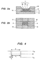
- Fig. 3A shows in cross-section a MIM electron emitter device in accordance with one preferred embodiment of the invention; and Fig. 3B depicts a plan view of the electron emitter.
- Fig. 4 is one exemplary waveform of a drive voltage signal as applied to the electron emitter shown in Figs. 3A and 3B.
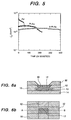
- Fig. 5 is a graph for demonstrating stability of emission current in the MIM electron emitter of Figs. 3A-3B.
- Fig. 6A shows a sectional view of a MIM electron emitter device in accordance with another embodiment of the invention.
- Fig. 3B depicts a plan view of the same.
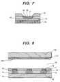
- Fig. 7 illustrates in cross-section a MIM electron emitter device in accordance with a still another embodiment of the invention.
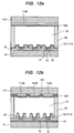
- Fig. 8 shows a sectional view of a display device in accordance with a yet another embodiment of the invention.
- Fig. 9 depicts a planar structure of the display device shown in Fig. 8.
- Fig. 10 is a circuit diagram of electrical driver circuitry as employed in the display device shown in Fig. 8.
- Fig. 11 is an illustration of a timing diagram showing the pulse sequence of drive voltage signals for operation of the display device of Figs. 8-10.
- Figs. 12A and 12B each depict a sectional view of a display device in accordance with a further embodiment of the invention.
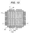
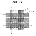
- Fig. 13 is a plan view of the display device of Figs. 12A-12B for showing the phosphor plane position thereof; and Fig. 14 illustrates another plan view thereof.
- Figs. 15A through 15G illustrate some of the major steps in the manufacture of a thin-film electron emitter for use in the display device of Figs. 12A to 14.
- Fig. 16 shows a perspective view of an EB lithography apparatus in accordance with a still further embodiment of the invention.
- the thin-film electron emitter has a multilayer structure that typically consists of an upper or "top” electrode 11 and a lower or “base” electrode 13 with an insulative or dielectric layer 12 being sandwiched between them.
- the top and base electrodes 11, 13 are electrically coupled to an associated direct current (DC) voltage source unit 20 to receive therefrom a drive voltage.
- DC direct current
- electron emission efficiency ⁇ may be determined by the ratio of a diode current Id flowing from base electrode 13 into top electrode 11 versus emission current Ie that is a current actually released toward vacuum 10, which efficiency Ie/Id may range from 10 -3 to 10 -5 .
- top electrode 11 has a three-layer structure of an interface layer 16, an intermediate or "middle" layer 17, and a surface layer 18.
- one characterizing feature of the electron emitter employing the invention lies in the fact that top electrode 11 is structured from the lamination of three layers: the interface layer 16, middle layer 17 and surface layer 18 as sequentially stacked on or above the underlying dielectric layer 12 in this order.
- the interface layer 16 will first be described as follows in connection with the illustration of Figs. 3A and 3B.
- the interface layer 16 is made of a specifically chosen material having increased sublimation enthalpy ⁇ Hs. The reason for such selection of high ⁇ Hs material is as follows.
- the mechanism for occurrence of degradation of the dielectric layer 12 upon application of strong electric field thereto is based on the "electromigration of the type in which the electrode-constituent atoms attempt by electric field to move or migrate into dielectric layers.”
- This electromigration occurrence mechanism may be treated as a model in such a way that upon application of a positive voltage to top electrode 11, atoms constituting the same are forced, by electric field created due to biassing, to sublime offering isolated atoms or atomic state, which may then be ionized by electric field within dielectric layer 12 allowing resultant ions to move or migrate due to the presence of such electric field.
- a structure of the middle layer 17 is as follows.
- the interface layer 16 will no longer remain as any continuous film when its thickness is less than or equal to 3 nanometers (nm); it tends to grow as islands during crystallization.
- Interface layer 16 principally attempts to fill or bury any possible gaps between such islands thereby acting to prevent surface layer 18 from being brought into contact with dielectric layer 12. More specifically, in situations where surface layer 18 comprised of gold (Au) or equivalents thereof is directly laminated on interface layer 16 without middle layer 17 laid therebetween, Au atoms or ions of lower sublimation enthalpy ⁇ Hs attempt to outdiffuse into dielectric layer 12 through gaps between film islands causing degradation of thin-film electron emitter.
- Au gold
- middle layer 17 is specifically provided which is greater in sublimation enthalpy Hs than surface layer 18.
- Table 1 below is presented to show the sublimation enthalpy ⁇ Hs and electrical resistivity as well as other material characteristic values involved, with respect to various kinds of metals.
- This graph shows certain experimental result which demonstrates the relation of the electron (current) emission efficiency Ie/Id versus a drive voltage in the electron emitter in accordance with the illustrative embodiment making use of the top electrode 11 consisting of lamination of interface layer 16 of 3-nm thick and Au-surface layer 18 of 6-nm thick.
- the same relation is also shown for an electron emitter having its top electrode consisting of an Au film of 9-nm thick only.
- the interface layer 16 of each sample here may be made of tungsten (W), iridium (Ir), or platinum (Pt).
- the dielectric layer 12 measures 5.5 nm in thickness.
- Dielectric layer 12 and top electrode 11 remain constant in thickness through all samples concerned, thereby to ensure that any possible differences in electron emission efficiency between or among samples successfully reflect the difference in transmittance of hot electrons among respective films each being contacted with dielectric layer 12 ⁇ that is, the W-, Ir-, Pt- and Au-films of 3-nm thick.
- the electron emission efficiency Ie/Id was such that Au (9 nm) offers a maximum value of 0.3%, Pt(3nm)-Au(6nm) is 0.1%, Ir(3nm)-Au(6nm) is 0.03%, and W(3nm)-Au(6nm) is 0.005%.
- the density of states in the vicinity of the Fermi level is mainly determined by how the d orbitals, which are localized in energy, are occupied in the metal, thereby it depends on the metal's electron configuration.
- certain metals high in sublimation enthalpy ⁇ Hs belong to transition metals covering from 3a to 8 groups, which remain less in electron emission efficiency Ie/Id than 1b-group metals such as gold (Au), silver (Ag) copper (Cu), and the like.
- the illustrative electron emitter device employing the invention has a specific film lamination structure with such middle layer laid between the upper and lower electrode layers.
- the transmittance of hot electrons inside metallic thin-films may be represented by exp(-d/ ⁇ ), where d is the thickness of a metal thin film, and ⁇ is the mean free path of hot electrons.
- d is the thickness of a metal thin film
- ⁇ is the mean free path of hot electrons.
- the resulting electron emission efficiency Ie/Id is from 0.2 to 0.25%, which may be substantially the same as that of the Au(9nm) metal.
- Ie/Id may increase up to 0.035 to 0.04%.
- the less the thickness d of metal thin film the greater the electron emission efficiency Ie/Id.
- the electron emission efficiency Ie/Id problem may be successfully avoided by rendering the film thickness d reduced.
- the interface layer 16 tends to grow into islands, any degradation will by no means take place in resultant thin-film electron emitter due to presence of the middle layer 17 between the top electrode 11 and base electrode 13 as best illustrated in Fig. 3A.
- Pt is more preferable for the middle layer while the same has been employed for the middle layer 17 in the experimentation of Fig. 2.
- Pt is less than Mo and Ir in possibility of occurrence of hot electron's scattering.
- Pt exhibits inherent nature that it tends to uniformly grow even when much reduced in thickness; consequently, this advantageously serves to prevent the surface-layer material from being accidentally brought into contact with the underlying dielectric layer 12 due to the fact that Pt resides between or among gaps of island-like grown interface layer 16.
- PUJPA No. 2-306520 wherein two layers are sequentially laminated on the dielectric layer 12 as follows: a first layer made of a negatively ionizable material such as aluminum (Al), cadmium (Cd), lead (Pb), or the like; and, a second layer of chemically stable material against microelectronics fabrication processes such as silver (Ag), molybdenum (Mo), tantalum (Ta), chromium (Cr), and gold (Au).
- a first layer made of a negatively ionizable material such as aluminum (Al), cadmium (Cd), lead (Pb), or the like
- a second layer of chemically stable material against microelectronics fabrication processes such as silver (Ag), molybdenum (Mo), tantalum (Ta), chromium (Cr), and gold (Au).
- the thin-film electron emitter is widely adaptable for use in a various types of electronics applications including, reduced-thickness high-resolution display apparatus, electron-beam (EB) photolithography apparatus and others.
- EB electron-beam
- the thin-film electron emitter is capable of stably emitting flow of electrons or current of high density while simultaneously permitting accomplishment of an array of rows and columns of electron emitters; accordingly, long life span and high luminance characteristics may be attained for both the display apparatus and EB lithography apparatus.
- the thin-film electron emitter application apparatus is arranged by use of a substrate having thereon a two-dimensional (2D) or areal array of electron emitters, which substrate is laminated with a face plate (referred to as the "front plate” hereinafter) having phosphors deposited on the surface thereof while sealing resultant laminated structure into vacuum environment.
- 2D two-dimensional
- front plate referred to as the "front plate” hereinafter
- the thin-film electron emitter application EB lithography equipment includes a three-layer structured thin-film electron emitter module, as the electron source, and an electron lens operatively associated therewith.
- the electron emitter module may include a substrate having a surface on which multiple thin-film electron emitter devices are arrayed in a 2D or areal matrix fashion, thereby offering capability of simultaneous transfer of an intended integrated circuit (IC) pattern onto a target wafer.
- IC integrated circuit
- Fig. 3B shows a plan view of the electron emitter whereas Fig. 3A depicts a corresponding cross-section of it taken along line A-B in Fig. 3B.
- the electron emitter includes an insulative substrate 14 which is made of glass, or the like.
- the glass substrate 14 has a surface on which a conductive film 13 which may be aluminum (Al) is formed to a predetermined thickness of, for example, 100 nm. This Al film acts as a lower or "base” electrode.
- Al aluminum
- radio-frequency (RF) magnetron sputtering techniques may be employed to form the Al base electrode film 13.
- Al film 13 is then subject to anode-oxidizing or anodization treatment on its exposed surface forming thereon an insulative or dielectric layer 12 to a thickness of 5.5 nm.
- the anodizing current for such anodization is limited in value enabling retainment of enhanced film quality for dielectric film 12.
- a chosen dielectric material such as SiO 2 , Al 2 O 3 or the like is deposited by RF-magnetron sputtering techniques to a thickness of 50 nm providing a protective layer 15.
- the pulse voltage used includes a train of pulse components of negative polarity at constant intervals t1 with a repeat period T, each of which has a potential level of -Vd1 set at -9 V and its pulse width tw being set at 64 microseconds ( s).
- each interval t1 between adjacent pulses may be 16.54 milliseconds (ms).
- Fig. 5 is a graph showing an aging-test measurement result which demonstrates the relation of peak-emission current density Je of resultant MIM electron emitter embodying the invention versus time elapsed, as labeled "Ir-Pt-Au” in Fig. 5.
- other emitter samples were also subject to similar aging test: one is with two-layer laminated top electrode structure consisting of a Pt interface layer of 3-nm thick and Au-surface layer of 3-nm thick, as labeled "Pt-Au"; the other, labeled "Au,” is with a single-layered top electrode structure consisting of Au film of 6-nm thick only.
- the Pt-Au two-layer structured top electrode is with extremely enhanced life-time characteristics as compared with the Au single-layered top electrode; however, especially where higher emission current is required, sufficient life-time characteristics are not attainable any more.
- the interface layer 16 is specifically comprised of Ir, its initial peak emission current density Je remains relatively low at about 2.5 mA/cm 2 ; instead, the stability is dramatically improved with the result of no decrease in emission current density Je being observed even after elapse of 400 minutes. This is because the use of Ir ⁇ this is higher than Pt in sublimation enthalpy ⁇ for interface layer 16 advantageously serves to further suppress occurrence of unwanted migration of the atoms constituting top electrode 11 toward dielectric layer 12.
- dielectric layer 12 as formed by anodization is further improved by use of high orientation films or single-crystalline films for the base electrode 13, leading to accomplishment of extra-high performance MIM electron emitters.
- dielectric layer 12 may alternatively be formed by sputtering or deposition techniques rather than anodization.
- interface layer 16 is of other, higher sublimation-enthalpy materials such as zirconium (Zr), hafnium (Hf), ruthenium (Ru), molybdenum (Mo), niobium (Nb), tantalum (Ta), rhenium (Re), osmium (Os), tungsten (W) or an alloy of plural elements as selected therefrom in cases where the middle layer 17 is comprised of Pt.
- Zr zirconium
- Hafnium hafnium
- Ru ruthenium
- Mo molybdenum
- Nb niobium
- Ta tantalum
- Re rhenium
- Os osmium
- W tungsten
- the surface layer 18 will not necessarily be formed; this layer 18 is not be required where the top electrode 11 per se exhibits "sufficiently" low electric resistivity without presence of surface layer 18.
- a second embodiment shown in Figs. 6A and 6B follows this approach, wherein Fig. 6B is a plan view whereas Fig. 6A is a cross-section thereof along line A-B.
- the illustrative thin-film electron emitter is structured from a lamination of interface layer 16 and middle layer 17 on dielectric layer 12.
- resultant electric resistivity of top electrode 11 is increased to be greater than that of the first embodiment, supra.
- top electrode 11 is electrically coupled via bus lines 32 to associative power-supply terminal nodes avoiding any problems otherwise possibly arising when top electrode 11 is high in resistivity to some extent.
- a MIS electron emitter in accordance with a third embodiment of the invention is shown in Fig. 7.
- an n-type silicon (Si) substrate is subject to oxidization by thermal anodization techniques, forming dielectric layer 12 thereon.
- a SiO 2 film is deposited by chemical vapor deposition (CVD) or sputtering techniques to a specified thickness, for example, 50 nm, providing a protective layer 15.
- CVD chemical vapor deposition
- sputtering techniques to a specified thickness, for example, 50 nm, providing a protective layer 15.
- a three-layered top electrode 11 is sequentially formed and laminated by RF-magnetron sputtering thereon.
- Figs. 8 and 9 illustrate one embodiment of display apparatus.
- Fig. 8 shows a cross-section of a planar structure shown in Fig. 9, which is a plan view of an array of rows and columns of electrodes of electron emitters on an insulative substrate of display apparatus.
- the substrate is not visible in Fig. 9 and is indicated by numeral 14 in Fig. 8B.
- the substrate 14 may be a glass substrate on which base electrode 13 is formed by RF sputtering method. During this process, patterning is performed as shown in Fig. 9 by use of an appropriate mask or a combination of photolithography and etching techniques. Subsequently, the dielectric layer 12 is formed by anodization.
- protective layer 15 of a chosen dielectric material, here SiO 2 is formed by RF-sputtering.
- Protective layer 15 functions to enhance the device life span by eliminating occurrence of dielectric breakdown otherwise taking place due to local concentration of electric field at side edges or corner portions of base electrode 13.
- sputtering is carried out sequentially forming three laminated films for top electrode 11.
- an Ir film of 1-nm thick is formed as interface layer 16; a Pt film of 2-nm thick is as middle layer 17; and an Au film of 6-nm thick as a surface layer 18.
- Resultant three-layer lamination is thus 9 nm in thickness as a whole.
- each lamination of the interface layer 16, middle layer 17 and surface layer 18 is selectively formed only at a corresponding one of intersections with base electrode 13.
- a chosen high-conductivity material, such as Au is formed to a thickness of 500 nm, thus having certain pattern shown in Fig. 8B.
- top-electrode bus lines 32 Resultant film patterned is used as top-electrode bus lines 32.
- the width of each bus line 32 is forced to be less than that of the top electrode 11 consisting of layers 16-18 at any locations other than top electrode 11, whereby it becomes possible to reduce inherent stray capacitance between top-electrode bus lines 32 and base electrodes 13 enabling achievement of high-speed device operations.
- a front plate 110 is made a rigid transparent material, such as glass, and has its inner surface on which an insulative transparent acceleration electrode 112 of indium-tin-oxide (ITO) is entirely formed by sputtering.
- ITO indium-tin-oxide
- a phosphor film 114 is coated by deposition on the ITO acceleration electrode 112.
- Phosphor film 114 may be made of a specific material capable of exhibiting high luminance or brightness efficiency even for low-energy electron beams used ⁇ ZnO:Zn is preferable.
- Front plate 110 with accelerator electrode 112 and phosphor film 114 on its inner surface is assembled with display substrate 14 having thereon an array of electron emitters by use of certain spacer (not shown) of 200-m thick which surrounds the periphery thereof; then, resultant structure is sealed using frit glass. An inner space defined between the substrate 14 and front plate 110 is next vacuumed completing the display panel 100 of display apparatus.
- Fig. 10 Electrical circuitry of the display panel 100 thus manufactured as operatively coupled to an associative driver circuit is shown in Fig. 10.
- the base electrodes 13 are connected to base-electrode driver circuits 41 whereas top-electrode bus lines 32 are tied to top-electrode driver circuits 42 respectively.
- the acceleration electrode 112 is operatively coupled to an acceleration-electrode driver circuit 43. Note that one dot at an intersection between the n-th base electrode 13 ⁇ say, Kn ⁇ and m-th top-electrode bus line 32Cm will be represented by (n, m) hereinafter, where "n" and "m" are integers.
- Fig. 11 shows waveforms of several major voltage signals as generated at nodes of respective driver circuits. Although not specifically indicated in this waveform diagram of Fig. 11, a voltage of 400V is constantly applied to the acceleration electrode 112.
- each electrode is at zero volts at a time point t0 resulting in no electrons being emitted therefrom; accordingly, the phosphor film 114 emits no rays of light.
- one base electrode 13K1 is applied with a voltage of -V 1 whereas top-electrode bus lines 32 as indicated by C1 and C2 receive a voltage of +V 2 .
- Certain voltage (V 1 + V 2 ) is applied between the base electrodes 13 and top electrodes 11 of dots (1, 1) and (1, 2); therefore, setting of this voltage (V 1 + V 2 ) at a predefined potential higher than the electron emission start potential may allow these two thin-film electron emitters to emit or liberate electrons into the vacuum space 10 of display panel 100. Electrons emitted are then accelerated by the voltage being applied to acceleration electrode 112 hitting phosphor film 114 to let it emit light.
- a voltage -V 1 is applied to the base electrode 13K2 while simultaneously applying voltage V 2 to a top-electrode bus line 32C1 causing a dot (2, 1) to turn on and emit light.
- Applying a set of the voltage waveforms of Fig. 11 in this way enables some selected dots with hatching in Fig. 10 to exclusively turn on.
- high-brightness/long-life display panels can be manufactured because of the fact that enhanced emission current density can be attained with increased stability and reliability.
- Fig. 13 is a plan view of a display panel as looked at from the face-plate side thereof
- Fig. 14 is a plan view of a display substrate 14 as viewed from its face-plate side.
- a cross-sectional view of each of the structures of Figs. 13 and 14 as taken along line A-B is shown in Figs. 12A whereas a cross-section along line C-D is illustrated in Fig. 12B with respect to the left-hand half portion thereof.
- FIG. 15A through 15G depict some of major steps in the manufacture of such thin-film electron emitters on display substrate 14.
- FIGs. 15A through 15G depict some of major steps in the manufacture of such thin-film electron emitters on display substrate 14.
- each of these figures comes with a combination of two different depictions, the right-hand side one of which is a plan view and the left-hand one is its associated cross-section which corresponds to that along line A-B in Figs. 13 and 14.
- Figs. 15A-15G is specifically drawn to only one electron emitter for purposes of illustration, it will be readily recognized by any person skilled in the art that similar devices are to be provided and organized into a 2D-matrix fashion on the same display substrate as shown in Figs. 12 and 14 when reduction to practice.
- an insulative substrate 15 made of glass or the like is prepared; then, a metallic thin film, such as Al film, is formed as the base electrode 13 on substrate 14 to a thickness of 300 nm, for example. Formation of this Al film may be done by sputtering, resistive heater deposition, molecular beam epitaxy (MBE), or the like. Next, this Al film is patterned by photolithographical resist formation and subsequent etching treatment, thereby defining therein a stripe-shaped pattern for formation of each base electrode 13.
- the resist used here may be any kinds of materials insofar as they are suitably adaptable for use with etching treatments, which may in turn be any one of wet etching and dry etching techniques.
- the base electrode 13 is subject to anodization process forming a dielectric layer 12 which measures 5 to 10 nm in thickness.
- the anodization voltage is set at 4 V for formation of dielectric layer of 5.5-nm thick.
- Resultant structure is as shown in Fig. 15A.
- a resist is deposited and irradiated with ultraviolet rays for patterning to thereby obtain a patterned resist mask 501 of Fig. 15B.
- Quinone diazide-based positive resist material may be employed as the mask.
- anodization is again carried out forming a protective layer 15.
- anodization current is set at 50 V or therearound for allowing protective film 15 to measure 70 nm in thickness. This is the state shown in Fig. 15C.
- this metal film is then formed as the top-electrode bus lines 32 on the entire surface of substrate 14.
- this metal film which will be patterned to define bus lines 32 therein has a multilayer lamination structure which includes a lower layer of certain metal exhibiting excellent adhesion with substrate 14, such as Mo, and an upper layer of hardly oxidizable metals with increased electrical conductivity, which layers are to be sequentially formed by sputtering or deposition.
- the lower Mo layer may alternatively be made of other metals, including Cr, with enhanced adhesionability with dielectric materials such as Ta, W, Nb or the like.
- the material for the upper layer Pt, Ir, Rh, Ru or the like may be used other than Au. With use of such metals, it is possible to retain an excellent electrical contact with an interface layer 16 to be later formed.
- the thickness of the metal film constituting the top-electrode bus lines 32 is modifiable pursuant to case-by-case requirements as to electrical resistivity of lead wires.
- the Mo film measured 30 nm in thickness whereas Au film was 100 nm thick.
- the resist mask 502 is removed away by known lift-off techniques using organic solution such as acetone, whereby resultant structure is as shown in Fig. 15E.
- a patterned resist mask 503 is formed as shown in Fig. 15F.
- Resultant structure is then put in a chosen anodization fluid for effecting anodization.
- the anodization current here may be similar in potential to that for formation of dielectric layer 12 ⁇ 4 volts, in this embodiment.
- Dielectric layer 12 which might be somewhat damaged by application of active chemicals, such as developing solution, through several resist-patterning process steps it has experienced until here.
- resultant structure is again subject to anodization prior to formation of its overlying top electrode. Thereafter, an interface layer 16, middle layer 17, and surface layer 18 are then formed in this order.
- an Ir film of 1-nm thick is formed as interface layer 16; a Pt film of 2-nm thick is as middle layer 17; and an Au film of 3-nm thick as a surface layer 18.
- the top electrode may comprise two layers which are, for example, the Ir interface layer 16 of 1-nm thick and Pt middle layer 17 of 2-nm thick with the surface layer 18 being deleted.
- the thin-film electron emitter is successfully formed on the display substrate 14.
- This electron emitter operates to emit electrons from certain region(s) as defined by the resist pattern 501. Since the thick dielectric film is formed covering peripheral portions of such electron emission part as the protective layer 15, an electric field created between the top and base electrodes will no longer attempt to locally concentrate on the side edges and/or corners of the base electrode, which in turn enables achievement of stable and reliable electron emission characteristics for an extended period of time.
- the front plate 110 may be made of transparent materials, including glass.
- a black matrix 120 is formed as shown in Fig. 12B.
- Black matrix 120 is arranged in layout to reside between adjacent ones of phosphors 114 shown in Fig. 13 although such is not visible in Fig. 13.
- the black matrix 120 may be fabricated as follows: deposit on front pate 120 solution of a mixture of graphite particles with polyvinyl alcohol (PVA) and ammonium di-chromate; irradiate UV rays for photographic exposure onto selected portions on each of which black matrix 120 is to be formed; and then, remove away non-exposed portions therefrom.
- PVA polyvinyl alcohol
- red phosphor material 114A is formed.
- front plate 110 is deposited on its surface with solution of a mixture of fluorescent particles with PVA and ammonium dichromate, UV rays are then irradiated for exposure onto selected portions being subject to phosphor-material formation; thereafter, any non-exposed portions are removed away using flow of water. In this way, red phosphor material 114A is patterned. Resultant pattern defined is as shown in Fig. 13B.
- the illustrative pattern is merely one example, and may be freely modified depending upon various display design requirements; for instance, it could be the so-called "RGBG" pattern which uses four neighboring dots for a single picture element or "pixel.”
- the phosphor film is equivalent in thickness to 1.4 to 2 layers of phosphor particles.
- a green phosphor material 11B and blue one 114C are formed in a way similar to that discussed above.
- the red phosphor material may be Y 2 O 2 :Eu (P22-R)
- green one may be Zn 2 SiO 4 :Mn (P1-G1)
- blue ZnS:Ag (P22-B).
- the red phosphor is YP 0.65 V 0.35 O 4 :Eu
- green is Zn 2 SiO 4 :Mn (P1-G1)
- blue is (Y,Gd)P 0.85 V 0.15 O 4 .
- an Al coat film is entirely deposited on front plate 110 to a thickness of approximately 50 to 300 mm, providing a metal back 122. Thereafter, plate 110 is heated up to 400 C or near permitting hydrolyzation of the filming film and organic film such as PVA, thereby completing front plate 110.
- front plate 110 and display substrate 14 are assembled together with an appropriate spacer being sandwiched therebetween at the periphery thereof, and are then frit-sealed by use of frit glass.
- the positional relation of front plate 110 versus substrate 14 for layout is as shown in Fig. 13.
- Fig. 14 the planar layout of thin-film electron emitter array thus formed on substrate 14 is depicted in a manner corresponding to the illustration of Fig. 13, although the protective layer 15 and top-electrode surface layer 18 are omitted therefrom for purposes of illustration only.
- the distance between spaced-apart front plate 14 and substrate 14 is from 1 to 3 mm.
- a spacer 60 is inserted therebetween for eliminating destruction of display panel due to application of external force under atmospheric pressure when and after the inside of such panel is vacuumed. Accordingly, in the case of manufacturing display apparatus having its display area of less than or equal to 4 cm (width) 9 cm (length) using a glass plate of 3-mm thick for front plate 110, spacer 60 will no longer be required. This can be said because plate 110 and substrate 14 with such size are capable of withstanding against application of such atmospheric pressure by their own mechanical or physical strength.
- the spacer 60 when used is arranged to have its shape as shown in Fig. 13.
- spacer support member is provided for every set of dots emitting red (R), green (G) and blue (B) light components, that is, for every set of three columns of top electrodes; however, such supports may be reduced in number as far as necessary mechanical strength is expectable.
- spacer 60 may be fabricated by defining, using sand-blasting method, openings or holes of a desired shape in a dielectric plate such as ceramics or glass.
- the seal-bonded display panel is vacuumed down at 1 10 -7 Torr for seal-packaging, thereby completing the display panel that makes use of several thin-film electron emitters embodying the invention.
- FIG. 16 An EB lithography apparatus in accordance with a sixth embodiment of the invention is shown in Fig. 16. While at least one electron emitter may be employed as the electron source in this EB lithography apparatus, this embodiment is specifically designed to employ a multi-electron emitter assembly 200 which includes an areal or 2D matrix of rows and columns of thin-film electron emitters.
- the multi-electron emitter unit 200 is similar in electrical driving method to the display apparatus in accordance with the fourth and fifth embodiments, supra, for emitting and projecting onto a target semiconductor wafer 240 an electron beam representative of a predefined pattern that corresponds to desired IC circuitry.
- the electron beam emitted is then guided to pass through a blanker 210; after leaving this, resultant beam is condensed by electron lens 220 by 1/1000 reduction in diameter providing a reduced-diameter spot beam, which is then deflected by deflecting system 230 and next projected onto wafer 240 so that the IC circuitry pattern is transferred thereonto.
- the required resist exposure remains less in time due to the fact that the emission electron density is high in addition to its capability of transferring plural IC patterns onto wafer 240 at a time. This may enable throughput to be much improved as compared with prior art EB systems.
- JPA Japanese Patent Application
Abstract
Description
- The present invention relates generally to electron source modules adaptable for use in electronic equipment, and more particularly to multilayer thin-film electron emitter devices as well as application equipment employing the same. The invention also relates to metal-insulator-metal (MIM) or metal-insulator-semiconductor (MIS) three-layer thin-film electron emitters and their application equipment including, but not limited to, display apparatus and electron beam (EB) lithography apparatus.
- Conventionally, thin-film electron emitter modules come with three-layered structure such as the MIM or MIS consisting of lamination of three thin films: an upper or "top" electrode, an intermediate or "middle" insulative layer, and a lower or "base" electrode. Upon application of an external potential between the top and base electrodes with the top electrode being positive in polarity, these MIM and MIS electron emitters operate to emit or liberate electrons from the surface of the top electrode into a vacuum. Until today, various types of electron emitters have been proposed, including those of the MIM type which employ metal for its top and base electrodes, and those of the MIS type making use of a semiconductor for at least one of such electrodes. One typical MIM electron emitter has been disclosed in, for example, Published Unexamined Japanese Patent Application (PUJPA) No. 7-65710.
- Principally, the operation of thin-film electron emitters is as follows. Upon application of a drive voltage between the top and base electrodes while potentially setting an electrical field within an insulative or dielectric layer sandwiched therebetween at 1 to 10 megavolts per centimeter (MV/cm) or greater, electrons which reside near or around the Fermi level in the base electrode are potentially activated to penetrate by tunnel effect through a barrier entering by injection into the conduction band of dielectric layer; thereafter, these electrons are accelerated to be further injected into the conduction band of the top electrode thereby behaving as the so-called "hot" electrons. Of those hot electrons, certain ones which have energy of more than the work function φ of top electrode are then released and emitted into the vacuum. By way of example, electron emission based on the above principle has been observed in a three-layer lamination electrode structure of Au-Al2O3-Al. This type of electron emitter offers in nature advantages as to performance and reliability: One advantage is that the electron emission characteristics will be substantially kept constant even when the work function φ varies due to occurrence of contamination on the surface of top electrode as caused by absorption of ambient gas therein. This renders them expectable as one of highly advanced electron emitters which is becoming important more and more in several applications.
- Unfortunately, the prior art electron emitters are faced with a serious problem that due to the necessity of applying to the dielectric layer a relatively strong electric field the intensity of which is as high as 1 to 10 MV/cm, degradation will possibly occur in the dielectric layer resulting in the so-called "forming" phenomenon as taught by PUJPA No. 7-226146, for example, which in turn disadvantageously leads to occurrence and mixture of noises in resultant flow of emitted electron or "current" while simultaneously resulting in electrical failure or breakdown which can lead to destruction of thin-film electron emitters in the worst case.
- The languageinsulative of dielectric layer" used herein includes semiconductors if their resistivity is high enough to tolerate the high electric field. An example of such thin-film electron emitters consists of silicon for the base electrode porous silicon for insulator, and metal for the top electrode, as is described in the Japanese Journal of Applied Physics, Vol. 34, Part 2, No. 6A, pp. L705 - L707 (1995).

- It is therefore an object of the present invention to provide a new and improved multilayer structure adaptable for use as basic lamination in electron emission source modules.
- It is another object of the invention to provide an electron source devices and apparatus employing the same capable of avoiding the problems faced with the prior art.
- It is a further object of the invention to provide an improved thin-film electron emitter device capable of suppressing or eliminating degradation in insulative layer used therein as well as electronics application equipment employing the same.
- The foregoing objects may be attained by the principles of the instant invention by providing specific multilayer thin-film structure including upper and lower electrodes with an insulative or dielectric layer being laid therebetween while letting the upper or "top" electrode be structured from a lamination of three layers ― that is, an surface layer, intermediate or "middle" layer and interface layer in this order. Very importantly, the middle layer is made of a chosen material which is greater in sublimation enthalpy than that constituting the surface layer and yet less in sublimation enthalpy than the interface layer.
- Where the top electrode remains sufficiently low in electrical resistivity, the surface layer will not always be required; in such cases, the top electrode may be in two-layer or double-layered structure essentially consisting of the interface layer and middle layer. The language "sufficiently low" as used herein may refer to certain degree of resistivity which is determinable depending upon several design requirements as to the device structure of thin-film electron emitters, desired emission current density, areal uniformity of electron emission, and the like. More specifically, it will be permissible that the electrical resistance of top electrode is increased in value either with a decrease in net area thereof or with a decrease in emission current density as required. Alternatively, in situations where the area uniformity of emission current is not so material in design requirement, a slight increase in resistivity of top electrode may be permitted to some degree. In such cases, the resistivity of the top electrode is considered to besufficiently low" without having to employ the surface layer as formed thereon.
- Preferably, the intermediate layer may be made of platinum (Pt) due to its inherent capability of being formed into a uniform, thin film as required.
- One significant advantage of the present invention is that an improved thin-film electron emitter of the MIM or MIS type may be accomplished capable of being free from the risk of occurrence of degradation when operated for long-run use. This is because of the fact that the top electrode is specifically structured from a lamination of three layers of thin films, including the interface layer, middle layer and surface layer while causing the middle layer to be greater in sublimation enthalpy than the surface layer and yet less than the interface layer.
- Another advantage of the invention is that enhanced emission current density can be attained with increased reliability and stability at any event due to optimization of the thickness of interface layer.
- Still another advantage is that in cases where the design requirements concerning retainment of increased conductivity of the top electrode is not so strict, the top electrode is allowed to comprise only two layer ― namely, the interface layer and middle layer ― with the surface layer unused. Here, the middle layer is made of Pt whereas the interface layer is of a chosen material having sublimation enthalpy greater than Pt.
- A further advantage of the invention is the thin-film electron emission devices thus arranged is adaptable for use in constituting several types of advanced electronics apparatus including, but not limited to, reduced-thickness high-resolution display panels thereby attaining enhanced illuminance characteristics while simultaneously increasing the life span and EB lithography apparatus thereby attaining operation speed as well as increasing lifespan thereof.
- These and other objects, features and advantages of the invention will be apparent from the following more particular description of preferred embodiments of the invention, as illustrated in the accompanying drawings.
- Fig. 1 is a diagrammatic representation for explanation of the operation in principle of a thin-film electron emitter.
- Fig. 2 is a graph showing the relation of the electron emission efficiency of the thin-film electron emitter versus drive voltage demonstrating the dependency of the former upon top-electrode materials.
- Fig. 3A shows in cross-section a MIM electron emitter device in accordance with one preferred embodiment of the invention; and Fig. 3B depicts a plan view of the electron emitter.
- Fig. 4 is one exemplary waveform of a drive voltage signal as applied to the electron emitter shown in Figs. 3A and 3B.
- Fig. 5 is a graph for demonstrating stability of emission current in the MIM electron emitter of Figs. 3A-3B.
- Fig. 6A shows a sectional view of a MIM electron emitter device in accordance with another embodiment of the invention; and Fig. 3B depicts a plan view of the same.
- Fig. 7 illustrates in cross-section a MIM electron emitter device in accordance with a still another embodiment of the invention.
- Fig. 8 shows a sectional view of a display device in accordance with a yet another embodiment of the invention.
- Fig. 9 depicts a planar structure of the display device shown in Fig. 8.
- Fig. 10 is a circuit diagram of electrical driver circuitry as employed in the display device shown in Fig. 8.
- Fig. 11 is an illustration of a timing diagram showing the pulse sequence of drive voltage signals for operation of the display device of Figs. 8-10.
- Figs. 12A and 12B each depict a sectional view of a display device in accordance with a further embodiment of the invention.
- Fig. 13 is a plan view of the display device of Figs. 12A-12B for showing the phosphor plane position thereof; and Fig. 14 illustrates another plan view thereof.
- Figs. 15A through 15G illustrate some of the major steps in the manufacture of a thin-film electron emitter for use in the display device of Figs. 12A to 14.
- Fig. 16 shows a perspective view of an EB lithography apparatus in accordance with a still further embodiment of the invention.
- Referring to Fig. 1, one typical thin-film electron emission source device is shown as a model for analyzing the principle of operation thereof for purposes of explanation only. As stated previously in the introductory part of the description, the thin-film electron emitter has a multilayer structure that typically consists of an upper or "top"
electrode 11 and a lower or "base"electrode 13 with an insulative ordielectric layer 12 being sandwiched between them. The top andbase electrodes voltage source unit 20 to receive therefrom a drive voltage. Upon application of such drive voltage between the top andbase electrodes dielectric layer 12 at larger than 1 to 10 MV/cm, electrons that reside near or around the Fermi level inbase electrode 13 attempt to pass through a potential barrier by tunnel effect rushing to flow by injection into the conduction band ofdielectric layer 12; then, these electrons are accelerated for further injection into the conduction band oftop electrode 11 acting as a packet of what is called the "hot" electrons. These hot electrons can contain therein specific ones which have an energy greater in work function φ thantop electrode 11; if this is the case, such "active" hot electrons will be externally released or liberated into a vacuum as designated by numeral 10 in Fig. 1. Here, the efficiency of flow of emitted electrons or "current" ― say, electron emission efficiency ― may be determined by the ratio of a diode current Id flowing frombase electrode 13 intotop electrode 11 versus emission current Ie that is a current actually released towardvacuum 10, which efficiency Ie/Id may range from 10-3 to 10-5. - See Fig. 3A, which shows a sectional view of a thin-film electron emitter in accordance with one preferred embodiment of the invention, which comes with the
top electrode 11 having a three-layer structure of aninterface layer 16, an intermediate or "middle"layer 17, and asurface layer 18. As shown, one characterizing feature of the electron emitter employing the invention lies in the fact thattop electrode 11 is structured from the lamination of three layers: theinterface layer 16,middle layer 17 andsurface layer 18 as sequentially stacked on or above the underlyingdielectric layer 12 in this order. - The
interface layer 16 will first be described as follows in connection with the illustration of Figs. 3A and 3B. With the illustrative embodiment of the invention, theinterface layer 16 is made of a specifically chosen material having increased sublimation enthalpy ΔHs. The reason for such selection of high ΔHs material is as follows. - As readily appreciated by a person skilled in the semiconductor art, it might be presumably considered that the mechanism for occurrence of degradation of the
dielectric layer 12 upon application of strong electric field thereto is based on the "electromigration of the type in which the electrode-constituent atoms attempt by electric field to move or migrate into dielectric layers." This electromigration occurrence mechanism may be treated as a model in such a way that upon application of a positive voltage totop electrode 11, atoms constituting the same are forced, by electric field created due to biassing, to sublime offering isolated atoms or atomic state, which may then be ionized by electric field withindielectric layer 12 allowing resultant ions to move or migrate due to the presence of such electric field. - Accordingly, the greater the energy required for the constituent atoms of
top electrode 11 to sublime (i.e., sublimation enthalpy ΔHs), the harder the occurrence of degradation ofdielectric layer 12. This is the very reason for employment of carefully chosen materials having increased sublimation enthalpy ΔHs for theinterface layer 16 oftop electrode 11. - Practically, as will be fully described in connection with Fig. 5 later, our experimentation demonstrated the fact that where several MIM electron emitters employing for
top electrode 11 various kinds of materials are under measurement, the operation stability thereof increases with an increase in sublimation enthalpy ΔHs of material being in contact withdielectric layer 12. - Additionally, such electromigration creation mechanism has been discussed in more detail in, for example, Journal of Electrochemical Society, Vol. 133, No. 6, pp. 1242-1246.
- A structure of the
middle layer 17 is as follows. Generally, theinterface layer 16 will no longer remain as any continuous film when its thickness is less than or equal to 3 nanometers (nm); it tends to grow as islands during crystallization.Interface layer 16 principally attempts to fill or bury any possible gaps between such islands thereby acting to preventsurface layer 18 from being brought into contact withdielectric layer 12. More specifically, in situations wheresurface layer 18 comprised of gold (Au) or equivalents thereof is directly laminated oninterface layer 16 withoutmiddle layer 17 laid therebetween, Au atoms or ions of lower sublimation enthalpy ΔHs attempt to outdiffuse intodielectric layer 12 through gaps between film islands causing degradation of thin-film electron emitter. To eliminate this outdiffusion,middle layer 17 is specifically provided which is greater in sublimation enthalpy Hs thansurface layer 18. Table 1 below is presented to show the sublimation enthalpy ΔHs and electrical resistivity as well as other material characteristic values involved, with respect to various kinds of metals.Group ΔHs (kcal) I.P. (eV) Work Function (eV) Resistivity (Ω-cm) Ag 1b 67.9 7.574 4.28 1.61 Al 3b 78.7 5.984 3.74 2.74 Cu 1b 80.5 7.724 4.47 1.7 Au 1b 88 9.22 4.7 2.2 Fd 8 90 8.33 4.82 10.55 Ti 4a 112.3 6.82 4.09 43.1 V 5a 122.9 6.74 4.11 19.9 Rh 8 133.1 7.46 4.65 4.78 Pt 8 135 9 5.29 10.42 Th 3a 137.5 - 3.41 15 Zr 4a 145.5 6.84 3.84 42.4 Hf 4a 148 7 3.53 30.6 Ru 8 154.9 7.364 4.52 7.37 Mo 6a 157 7.1 4.27 5.33 Tc 7a 158 7.28 - - Ir 8 160 9 4.57 5.07 Nb 5a 172.4 6.88 3.99 14.5 Ta 5a 186 7.88 4.12 13.1 Re 7a 186.1 7.87 5.1 18.6 Os 8 189 8.7 4.55 9.13 W 6a 203.4 7.98 4.5 5.33 - As can be seen from Table 1 above, materials with high sublimation enthalpy ΔHs tend to exhibit relatively high electrical resistivity.
- See Fig. 2. This graph shows certain experimental result which demonstrates the relation of the electron (current) emission efficiency Ie/Id versus a drive voltage in the electron emitter in accordance with the illustrative embodiment making use of the
top electrode 11 consisting of lamination ofinterface layer 16 of 3-nm thick and Au-surface layer 18 of 6-nm thick. In this graph, as a comparative example, the same relation is also shown for an electron emitter having its top electrode consisting of an Au film of 9-nm thick only. Theinterface layer 16 of each sample here may be made of tungsten (W), iridium (Ir), or platinum (Pt). Thedielectric layer 12 measures 5.5 nm in thickness.Dielectric layer 12 andtop electrode 11 remain constant in thickness through all samples concerned, thereby to ensure that any possible differences in electron emission efficiency between or among samples successfully reflect the difference in transmittance of hot electrons among respective films each being contacted withdielectric layer 12 ― that is, the W-, Ir-, Pt- and Au-films of 3-nm thick. Upon application of a drive voltage of 6.5 volts (V), the electron emission efficiency Ie/Id was such that Au (9 nm) offers a maximum value of 0.3%, Pt(3nm)-Au(6nm) is 0.1%, Ir(3nm)-Au(6nm) is 0.03%, and W(3nm)-Au(6nm) is 0.005%. This tells that the electron emission efficiency Ie/Id decreases in percentage value with a decrease in group number of metals in the atom's periodic table. This tendency is originated from the fact that the hot electron's transmittance with respect to the top electrode of electron emitter is determined by electron-electron scattering as occurred inside metals. Because of the principle of energy conservation, the cross-section of the electron-electron scattering increases as the density of states of the top electrode increases. More specifically, when the kinetic energy of the hot electron is E0 (measured in reference to the Fermi level of the top electrode), the scattering cross-section is mainly determined by the density of states integrated in the energy range from -E0 to E0. The density of states in the vicinity of the Fermi level is mainly determined by how the d orbitals, which are localized in energy, are occupied in the metal, thereby it depends on the metal's electron configuration. The density of states near the Fermi level, and thus the scattering cross-section change in the ascending order: groups 1b and 2b <group 8 < group 7a < groups 6a, 5a, 4a, and 3a in the periodic table. Typically, certain metals high in sublimation enthalpy ΔHs belong to transition metals covering from 3a to 8 groups, which remain less in electron emission efficiency Ie/Id than 1b-group metals such as gold (Au), silver (Ag) copper (Cu), and the like. The illustrative electron emitter device employing the invention has a specific film lamination structure with such middle layer laid between the upper and lower electrode layers. - One possible approach to attain high emission current Ie is rendering the
interface layer 16 thinner. The transmittance of hot electrons inside metallic thin-films may be represented by exp(-d/λ), where d is the thickness of a metal thin film, and λ is the mean free path of hot electrons. As a consequence, if the thickness of the foregoinginterface layer 16 is rendered thinner to measure 1 nm, by way of example, then resultant hot electron's transmittance may increase by approximately seven, to eight times than ever. Hence, where the Ir(1nm)-Au(6nm) stacked structure is employed fortop electrode 11 rather than the Ir(3nm)-Au(6nm) stacked structure as used in the structure of Fig. 2, the resulting electron emission efficiency Ie/Id is from 0.2 to 0.25%, which may be substantially the same as that of the Au(9nm) metal. Alternatively, with the use of W(1nm)-Au(6nm) alloy, Ie/Id may increase up to 0.035 to 0.04%. Apparently, the less the thickness d of metal thin film, the greater the electron emission efficiency Ie/Id. In this way, even in cases of employing metal films of relatively high sublimation enthalpy ΔHs such as Ir, W or the like, the electron emission efficiency Ie/Id problem may be successfully avoided by rendering the film thickness d reduced. In such cases, while theinterface layer 16 tends to grow into islands, any degradation will by no means take place in resultant thin-film electron emitter due to presence of themiddle layer 17 between thetop electrode 11 andbase electrode 13 as best illustrated in Fig. 3A. - Note here that Pt is more preferable for the middle layer while the same has been employed for the
middle layer 17 in the experimentation of Fig. 2. As readily seen from Fig. 2, Pt is less than Mo and Ir in possibility of occurrence of hot electron's scattering. Moreover, Pt exhibits inherent nature that it tends to uniformly grow even when much reduced in thickness; consequently, this advantageously serves to prevent the surface-layer material from being accidentally brought into contact with theunderlying dielectric layer 12 due to the fact that Pt resides between or among gaps of island-likegrown interface layer 16. - The description is now directed to certain cases that do not require formation of the
surface layer 18. By way of example, consider the case where a layer for defining therein electrical lead wires for exclusive use as power supply lines (say, bus lines) is arranged so as to be in physical contact with thetop electrode 11 in order to supply it with necessary power supply voltage, thereby moderating or softening technical requirements as to electrical resistivity fortop electrode 11. - It should be noted that one prior known two-layer structure for the top electrode has been disclosed in, for example, PUJPA No. 2-306520, wherein two layers are sequentially laminated on the
dielectric layer 12 as follows: a first layer made of a negatively ionizable material such as aluminum (Al), cadmium (Cd), lead (Pb), or the like; and, a second layer of chemically stable material against microelectronics fabrication processes such as silver (Ag), molybdenum (Mo), tantalum (Ta), chromium (Cr), and gold (Au). Unfortunately, this prior art approach disclosed therein is encountered with a problem that the material selected to constitute the first layer remains less in sublimation enthalpy ΔHs ― such as 78.7 kilo-calories (kcal) for Al, 26.7 kcal for Cd, and 46.78 for Pb ― and more seriously, the aforesaid material is even less in sublimation enthalpy than Au (88 kcal) which is one of materials preferably employed for the second layer and yet is the representative one for preferable use as thesurface layer 18 in accordance with the illustrative embodiment of the invention. This may render the present invention patentably distinguishable in principal concept over the prior art mentioned above. - Attention should be paid to the fact that the thin-film electron emitter is widely adaptable for use in a various types of electronics applications including, reduced-thickness high-resolution display apparatus, electron-beam (EB) photolithography apparatus and others. In regard to such application apparatus or equipment, since the thin-film electron emitter is capable of stably emitting flow of electrons or current of high density while simultaneously permitting accomplishment of an array of rows and columns of electron emitters; accordingly, long life span and high luminance characteristics may be attained for both the display apparatus and EB lithography apparatus.
- One example is that the thin-film electron emitter application apparatus is arranged by use of a substrate having thereon a two-dimensional (2D) or areal array of electron emitters, which substrate is laminated with a face plate (referred to as the "front plate" hereinafter) having phosphors deposited on the surface thereof while sealing resultant laminated structure into vacuum environment.
- Another example is that the thin-film electron emitter application EB lithography equipment includes a three-layer structured thin-film electron emitter module, as the electron source, and an electron lens operatively associated therewith. In this case, the electron emitter module may include a substrate having a surface on which multiple thin-film electron emitter devices are arrayed in a 2D or areal matrix fashion, thereby offering capability of simultaneous transfer of an intended integrated circuit (IC) pattern onto a target wafer.
- Several embodiments of the invention will now be fully described with reference to the accompanying drawings.
- Referring now to Figs. 3A and 3B, main part of a thin-film electron source is shown which will be called the "electron emitter" hereinafter. Fig. 3B shows a plan view of the electron emitter whereas Fig. 3A depicts a corresponding cross-section of it taken along line A-B in Fig. 3B. The electron emitter includes an
insulative substrate 14 which is made of glass, or the like. Theglass substrate 14 has a surface on which aconductive film 13 which may be aluminum (Al) is formed to a predetermined thickness of, for example, 100 nm. This Al film acts as a lower or "base" electrode. Here, radio-frequency (RF) magnetron sputtering techniques may be employed to form the Albase electrode film 13.Al film 13 is then subject to anode-oxidizing or anodization treatment on its exposed surface forming thereon an insulative ordielectric layer 12 to a thickness of 5.5 nm. The anodizing current for such anodization is limited in value enabling retainment of enhanced film quality fordielectric film 12. Then, a chosen dielectric material such as SiO2, Al2O3 or the like is deposited by RF-magnetron sputtering techniques to a thickness of 50 nm providing aprotective layer 15. Subsequently, another Al film is continuously formed by similar sputtering techniques in a vacuum atmosphere providing an upper or "top" electrode of three-layer lamination structure. At this time, three films are sequentially formed: an Ir film of 1-nm thick as aninterface layer 16; a Pt film of 2-nm thick as an intermediate or "middle"layer 17; and an Au film of 3-nm thick as asurface layer 18. Resultant three-layerlamination structure measures 6 nm in thickness as a whole. Finally, a patterned Au layer is formed providing abus line pattern 32 for thetop electrode 11. - Then, resultant structure is placed in a vacuum chamber (not shown) at selected degree of vacuum of 10-7 Torr for application of a pulse voltage to the
base electrode 13 with top-electrode bus lines 32 being grounded in potential, thereby insuring the operation stability. As shown in Fig. 4, the pulse voltage used includes a train of pulse components of negative polarity at constant intervals t1 with a repeat period T, each of which has a potential level of -Vd1 set at -9 V and its pulse width tw being set at 64 microseconds ( s). Here, each interval t1 between adjacent pulses may be 16.54 milliseconds (ms). In other words, first apply a pulsate voltage of -Vd1 = -9 V for preselected pulse width tw = 64 s; then apply a voltage of Vd2 = 0 V for a time period of 16.54 ms. This pulse cycle will be repeated with period T = 16.6 ms. Note that the repeat period T and pulse width tw may be modified in value as required; for instance, period T may range from 2 s to 1000 ms whereas tw = 1 s to 500 ms. In this respect, as taught by the PUJPA No. 7-226146, supra, the MIM electron emitter will be further improved in stability by modifying the voltage Vd2 to positively shift in potential falling within a range of Vd2 = +1 to +5 volts. - Fig. 5 is a graph showing an aging-test measurement result which demonstrates the relation of peak-emission current density Je of resultant MIM electron emitter embodying the invention versus time elapsed, as labeled "Ir-Pt-Au" in Fig. 5. For a comparison, other emitter samples were also subject to similar aging test: one is with two-layer laminated top electrode structure consisting of a Pt interface layer of 3-nm thick and Au-surface layer of 3-nm thick, as labeled "Pt-Au"; the other, labeled "Au," is with a single-layered top electrode structure consisting of Au film of 6-nm thick only. For these three different MIM electron emitters, an application voltage was set at fixed levels to ensure that diode current Id is kept constant among them; and simultaneously, electric field being applied to
dielectric layer 12 of each sample is identical to those of the others. As can be readily seen by a person skilled in the art from the graph of Fig. 5, with the Au single-layer structure, while the current density Je is initially high in value due to the significance of its electron emission efficiency Ie/Id, Je tends to decrease with time; after elapse of 50 minutes, electron emission finally ceases. With Pt-Au two-layer structure, while the initial peak emission current density Je is high as 2 milliamperes per square centimeter (mA/cm2), it steeply drops down after elapse of approximately 400 minutes. In this way, the Pt-Au two-layer structured top electrode is with extremely enhanced life-time characteristics as compared with the Au single-layered top electrode; however, especially where higher emission current is required, sufficient life-time characteristics are not attainable any more. In contrast, with the Ir-Pt-Au three-layer structure embodying the invention, since theinterface layer 16 is specifically comprised of Ir, its initial peak emission current density Je remains relatively low at about 2.5 mA/cm2; instead, the stability is dramatically improved with the result of no decrease in emission current density Je being observed even after elapse of 400 minutes. This is because the use of Ir ― this is higher than Pt in sublimation enthalpy ― forinterface layer 16 advantageously serves to further suppress occurrence of unwanted migration of the atoms constitutingtop electrode 11 towarddielectric layer 12. - It should be noted in this embodiment that the characteristics of
dielectric layer 12 as formed by anodization is further improved by use of high orientation films or single-crystalline films for thebase electrode 13, leading to accomplishment of extra-high performance MIM electron emitters. In addition,dielectric layer 12 may alternatively be formed by sputtering or deposition techniques rather than anodization. - It should also be noted that while the foregoing is drawn to one specific embodiment with the
interface layer 16 made of Ir, similar advantages will be attained ifinterface layer 16 is of other, higher sublimation-enthalpy materials such as zirconium (Zr), hafnium (Hf), ruthenium (Ru), molybdenum (Mo), niobium (Nb), tantalum (Ta), rhenium (Re), osmium (Os), tungsten (W) or an alloy of plural elements as selected therefrom in cases where themiddle layer 17 is comprised of Pt. - In the first embodiment set forth above, the
surface layer 18 will not necessarily be formed; thislayer 18 is not be required where thetop electrode 11 per se exhibits "sufficiently" low electric resistivity without presence ofsurface layer 18. A second embodiment shown in Figs. 6A and 6B follows this approach, wherein Fig. 6B is a plan view whereas Fig. 6A is a cross-section thereof along line A-B. As shown in Fig. 6A, the illustrative thin-film electron emitter is structured from a lamination ofinterface layer 16 andmiddle layer 17 ondielectric layer 12. In this case, resultant electric resistivity oftop electrode 11 is increased to be greater than that of the first embodiment, supra. To compensate for this,top electrode 11 is electrically coupled viabus lines 32 to associative power-supply terminal nodes avoiding any problems otherwise possibly arising whentop electrode 11 is high in resistivity to some extent. - A MIS electron emitter in accordance with a third embodiment of the invention is shown in Fig. 7. As shown, an n-type silicon (Si) substrate is subject to oxidization by thermal anodization techniques, forming
dielectric layer 12 thereon. Then, a SiO2 film is deposited by chemical vapor deposition (CVD) or sputtering techniques to a specified thickness, for example, 50 nm, providing aprotective layer 15. Next, a three-layeredtop electrode 11 is sequentially formed and laminated by RF-magnetron sputtering thereon. Formation of three films during this process is as follows: an Ir film of 1-nm thick asinterface layer 16; a Pt film of 2-nm thick is asmiddle layer 17; and an Au film of 3-nm thick assurface layer 18. Resultant three-layer lamination is 6 nm in thickness as a whole. Finally, a patterned Au layer is formed providing thebus line pattern 32 fortop electrode 11. - An explanation will now be given of application equipment employing one or several thin-film electron emitters embodying the invention.
- Figs. 8 and 9 illustrate one embodiment of display apparatus. Fig. 8 shows a cross-section of a planar structure shown in Fig. 9, which is a plan view of an array of rows and columns of electrodes of electron emitters on an insulative substrate of display apparatus. The substrate is not visible in Fig. 9 and is indicated by numeral 14 in Fig. 8B. The
substrate 14 may be a glass substrate on whichbase electrode 13 is formed by RF sputtering method. During this process, patterning is performed as shown in Fig. 9 by use of an appropriate mask or a combination of photolithography and etching techniques. Subsequently, thedielectric layer 12 is formed by anodization. Next,protective layer 15 of a chosen dielectric material, here SiO2, is formed by RF-sputtering.Protective layer 15 functions to enhance the device life span by eliminating occurrence of dielectric breakdown otherwise taking place due to local concentration of electric field at side edges or corner portions ofbase electrode 13. - Next, sputtering is carried out sequentially forming three laminated films for
top electrode 11. At this time, an Ir film of 1-nm thick is formed asinterface layer 16; a Pt film of 2-nm thick is asmiddle layer 17; and an Au film of 6-nm thick as asurface layer 18. Resultant three-layer lamination is thus 9 nm in thickness as a whole. As shown in Fig. 9, each lamination of theinterface layer 16,middle layer 17 andsurface layer 18 is selectively formed only at a corresponding one of intersections withbase electrode 13. Subsequently, a chosen high-conductivity material, such as Au, is formed to a thickness of 500 nm, thus having certain pattern shown in Fig. 8B. Resultant film patterned is used as top-electrode bus lines 32. As shown in Fig. 8B, the width of eachbus line 32 is forced to be less than that of thetop electrode 11 consisting of layers 16-18 at any locations other thantop electrode 11, whereby it becomes possible to reduce inherent stray capacitance between top-electrode bus lines 32 andbase electrodes 13 enabling achievement of high-speed device operations. - As shown in Fig. 8, a
front plate 110 is made a rigid transparent material, such as glass, and has its inner surface on which an insulativetransparent acceleration electrode 112 of indium-tin-oxide (ITO) is entirely formed by sputtering. Aphosphor film 114 is coated by deposition on theITO acceleration electrode 112.Phosphor film 114 may be made of a specific material capable of exhibiting high luminance or brightness efficiency even for low-energy electron beams used ― ZnO:Zn is preferable.Front plate 110 withaccelerator electrode 112 andphosphor film 114 on its inner surface is assembled withdisplay substrate 14 having thereon an array of electron emitters by use of certain spacer (not shown) of 200-m thick which surrounds the periphery thereof; then, resultant structure is sealed using frit glass. An inner space defined between thesubstrate 14 andfront plate 110 is next vacuumed completing thedisplay panel 100 of display apparatus. - Electrical circuitry of the
display panel 100 thus manufactured as operatively coupled to an associative driver circuit is shown in Fig. 10. Thebase electrodes 13 are connected to base-electrode driver circuits 41 whereas top-electrode bus lines 32 are tied to top-electrode driver circuits 42 respectively. Theacceleration electrode 112 is operatively coupled to an acceleration-electrode driver circuit 43. Note that one dot at an intersection between the n-th base electrode 13 ― say, Kn ― and m-th top-electrode bus line 32Cm will be represented by (n, m) hereinafter, where "n" and "m" are integers. - See Fig. 11, which shows waveforms of several major voltage signals as generated at nodes of respective driver circuits. Although not specifically indicated in this waveform diagram of Fig. 11, a voltage of 400V is constantly applied to the
acceleration electrode 112. - As can be seen from Fig. 11, each electrode is at zero volts at a time point t0 resulting in no electrons being emitted therefrom; accordingly, the
phosphor film 114 emits no rays of light. - At time t1 of Fig. 11, one base electrode 13K1 is applied with a voltage of -V1 whereas top-
electrode bus lines 32 as indicated by C1 and C2 receive a voltage of +V2. Certain voltage (V1 + V2) is applied between thebase electrodes 13 andtop electrodes 11 of dots (1, 1) and (1, 2); therefore, setting of this voltage (V1 + V2) at a predefined potential higher than the electron emission start potential may allow these two thin-film electron emitters to emit or liberate electrons into thevacuum space 10 ofdisplay panel 100. Electrons emitted are then accelerated by the voltage being applied toacceleration electrode 112 hittingphosphor film 114 to let it emit light. - Then, at time t2 of Fig. 11, a voltage -V1 is applied to the base electrode 13K2 while simultaneously applying voltage V2 to a top-electrode bus line 32C1 causing a dot (2, 1) to turn on and emit light. Applying a set of the voltage waveforms of Fig. 11 in this way enables some selected dots with hatching in Fig. 10 to exclusively turn on.
- In the way as set forth above, it becomes possible to display any desired images or information by changing or modifying the signals being applied to top-electrode bus lines 32. Also, It is possible to visually indicate multiple gray-scale images by suitably changing the intensity of voltage signal V1 applied to top-
electrode bus lines 32 depending upon an image signal required. - With use of the thin-film electron emitters embodying the invention, high-brightness/long-life display panels can be manufactured because of the fact that enhanced emission current density can be attained with increased stability and reliability.
- Other examples employing the principle of the present invention will now be described in connection with Figs. 12-15. Fig. 13 is a plan view of a display panel as looked at from the face-plate side thereof, whereas Fig. 14 is a plan view of a
display substrate 14 as viewed from its face-plate side. A cross-sectional view of each of the structures of Figs. 13 and 14 as taken along line A-B is shown in Figs. 12A whereas a cross-section along line C-D is illustrated in Fig. 12B with respect to the left-hand half portion thereof. - A manufacturing method of thin-film electron emitters to be formed on the display substrate is as follows. See Figs. 15A through 15G, which depict some of major steps in the manufacture of such thin-film electron emitters on
display substrate 14. Note here that, for purposes of explanation, each of these figures comes with a combination of two different depictions, the right-hand side one of which is a plan view and the left-hand one is its associated cross-section which corresponds to that along line A-B in Figs. 13 and 14. Note also that while Figs. 15A-15G is specifically drawn to only one electron emitter for purposes of illustration, it will be readily recognized by any person skilled in the art that similar devices are to be provided and organized into a 2D-matrix fashion on the same display substrate as shown in Figs. 12 and 14 when reduction to practice. - First, as shown in Fig. 15A, an
insulative substrate 15 made of glass or the like is prepared; then, a metallic thin film, such as Al film, is formed as thebase electrode 13 onsubstrate 14 to a thickness of 300 nm, for example. Formation of this Al film may be done by sputtering, resistive heater deposition, molecular beam epitaxy (MBE), or the like. Next, this Al film is patterned by photolithographical resist formation and subsequent etching treatment, thereby defining therein a stripe-shaped pattern for formation of eachbase electrode 13. The resist used here may be any kinds of materials insofar as they are suitably adaptable for use with etching treatments, which may in turn be any one of wet etching and dry etching techniques. Thebase electrode 13 is subject to anodization process forming adielectric layer 12 which measures 5 to 10 nm in thickness. In this embodiment, the anodization voltage is set at 4 V for formation of dielectric layer of 5.5-nm thick. Resultant structure is as shown in Fig. 15A. - Then, as shown in Fig. 15B, a resist is deposited and irradiated with ultraviolet rays for patterning to thereby obtain a patterned resist
mask 501 of Fig. 15B. Quinone diazide-based positive resist material may be employed as the mask. With the patterned resistmask 501 being left thereon, anodization is again carried out forming aprotective layer 15. During this second anodization process, anodization current is set at 50 V or therearound for allowingprotective film 15 to measure 70 nm in thickness. This is the state shown in Fig. 15C. - After resist
mask 501 is removed away using chosen organic solvent such as acetone, similar process is applied to form another patterned resistmask 502 as shown in Fig. 15D. A metal film is then formed as the top-electrode bus lines 32 on the entire surface ofsubstrate 14. Preferably, this metal film which will be patterned to definebus lines 32 therein has a multilayer lamination structure which includes a lower layer of certain metal exhibiting excellent adhesion withsubstrate 14, such as Mo, and an upper layer of hardly oxidizable metals with increased electrical conductivity, which layers are to be sequentially formed by sputtering or deposition. The lower Mo layer may alternatively be made of other metals, including Cr, with enhanced adhesionability with dielectric materials such as Ta, W, Nb or the like. As the material for the upper layer, Pt, Ir, Rh, Ru or the like may be used other than Au. With use of such metals, it is possible to retain an excellent electrical contact with aninterface layer 16 to be later formed. Note here that the thickness of the metal film constituting the top-electrode bus lines 32 is modifiable pursuant to case-by-case requirements as to electrical resistivity of lead wires. By way of example, in this embodiment, the Mo film measured 30 nm in thickness whereas Au film was 100 nm thick. Thereafter, the resistmask 502 is removed away by known lift-off techniques using organic solution such as acetone, whereby resultant structure is as shown in Fig. 15E. - Subsequently, a patterned resist
mask 503 is formed as shown in Fig. 15F. Resultant structure is then put in a chosen anodization fluid for effecting anodization. The anodization current here may be similar in potential to that for formation ofdielectric layer 12 ― 4 volts, in this embodiment.Dielectric layer 12 which might be somewhat damaged by application of active chemicals, such as developing solution, through several resist-patterning process steps it has experienced until here. To cure this layer, resultant structure is again subject to anodization prior to formation of its overlying top electrode. Thereafter, aninterface layer 16,middle layer 17, andsurface layer 18 are then formed in this order. For formation of these films, sputtering is to be used while ensuring that each layer is continuously formed without having to destroy or disturb vacuum environments. In this embodiment, an Ir film of 1-nm thick is formed asinterface layer 16; a Pt film of 2-nm thick is asmiddle layer 17; and an Au film of 3-nm thick as asurface layer 18. Alternatively, like this embodiment, in cases where thebus lines 32 for exclusively supplying an application voltage to the top electrode are specifically employed while the top electrode remains less in area, the top electrode may comprise two layers which are, for example, theIr interface layer 16 of 1-nm thick and Ptmiddle layer 17 of 2-nm thick with thesurface layer 18 being deleted. - Subsequently, the last formed resist is removed away by lift-off techniques using organic solution such as acetone, completing an intended thin-film electron emitter as shown in Fig. 15G. By using the foregoing fabrication scheme, the thin-film electron emitter is successfully formed on the
display substrate 14. This electron emitter operates to emit electrons from certain region(s) as defined by the resistpattern 501. Since the thick dielectric film is formed covering peripheral portions of such electron emission part as theprotective layer 15, an electric field created between the top and base electrodes will no longer attempt to locally concentrate on the side edges and/or corners of the base electrode, which in turn enables achievement of stable and reliable electron emission characteristics for an extended period of time. - Turning now to Figs. 12A and 12B, the
front plate 110 may be made of transparent materials, including glass. First, ablack matrix 120 is formed as shown in Fig. 12B.Black matrix 120 is arranged in layout to reside between adjacent ones ofphosphors 114 shown in Fig. 13 although such is not visible in Fig. 13. - The
black matrix 120 may be fabricated as follows: deposit onfront pate 120 solution of a mixture of graphite particles with polyvinyl alcohol (PVA) and ammonium di-chromate; irradiate UV rays for photographic exposure onto selected portions on each of whichblack matrix 120 is to be formed; and then, remove away non-exposed portions therefrom. - Then, a
red phosphor material 114A is formed. Afterfront plate 110 is deposited on its surface with solution of a mixture of fluorescent particles with PVA and ammonium dichromate, UV rays are then irradiated for exposure onto selected portions being subject to phosphor-material formation; thereafter, any non-exposed portions are removed away using flow of water. In this way,red phosphor material 114A is patterned. Resultant pattern defined is as shown in Fig. 13B. The illustrative pattern is merely one example, and may be freely modified depending upon various display design requirements; for instance, it could be the so-called "RGBG" pattern which uses four neighboring dots for a single picture element or "pixel." The phosphor film is equivalent in thickness to 1.4 to 2 layers of phosphor particles. A green phosphor material 11B and blue one 114C are formed in a way similar to that discussed above. By way of example, the red phosphor material may be Y2O2:Eu (P22-R), green one may be Zn2SiO4:Mn (P1-G1), and blue be ZnS:Ag (P22-B). Alternatively, the red phosphor is YP0.65V0.35O4:Eu, green is Zn2SiO4:Mn (P1-G1), and blue is (Y,Gd)P0.85V0.15O4. - Next, after filming is performed by use of a nitrocellulose film or the like, an Al coat film is entirely deposited on
front plate 110 to a thickness of approximately 50 to 300 mm, providing a metal back 122. Thereafter,plate 110 is heated up to 400 C or near permitting hydrolyzation of the filming film and organic film such as PVA, thereby completingfront plate 110. - The resulting
front plate 110 anddisplay substrate 14 are assembled together with an appropriate spacer being sandwiched therebetween at the periphery thereof, and are then frit-sealed by use of frit glass. The positional relation offront plate 110 versussubstrate 14 for layout is as shown in Fig. 13. In Fig. 14, the planar layout of thin-film electron emitter array thus formed onsubstrate 14 is depicted in a manner corresponding to the illustration of Fig. 13, although theprotective layer 15 and top-electrode surface layer 18 are omitted therefrom for purposes of illustration only. - The distance between spaced-apart
front plate 14 andsubstrate 14 is from 1 to 3 mm. Aspacer 60 is inserted therebetween for eliminating destruction of display panel due to application of external force under atmospheric pressure when and after the inside of such panel is vacuumed. Accordingly, in the case of manufacturing display apparatus having its display area of less than or equal to 4 cm (width) 9 cm (length) using a glass plate of 3-mm thick forfront plate 110,spacer 60 will no longer be required. This can be said becauseplate 110 andsubstrate 14 with such size are capable of withstanding against application of such atmospheric pressure by their own mechanical or physical strength. Thespacer 60 when used is arranged to have its shape as shown in Fig. 13. Here, one spacer support member is provided for every set of dots emitting red (R), green (G) and blue (B) light components, that is, for every set of three columns of top electrodes; however, such supports may be reduced in number as far as necessary mechanical strength is expectable.Such spacer 60 may be fabricated by defining, using sand-blasting method, openings or holes of a desired shape in a dielectric plate such as ceramics or glass. - The seal-bonded display panel is vacuumed down at 1 10-7 Torr for seal-packaging, thereby completing the display panel that makes use of several thin-film electron emitters embodying the invention.
- With this embodiment, since the distance between the
front plate 110 andsubstrate 14 is as long as 1 to 3 mm, it becomes possible to increase an acceleration voltage to the metal back 122 up to 3 to 6 kV. Accordingly, as stated previously, presently available phosphor materials for use in cathode-ray tube (CRT) units may be employed as thephosphor material 114. Voltage waveforms of several drive signals as used in this embodiment is similar to those in the forth embodiment with the acceleration voltage here being replaced by a high potential of 3 to 6 kV. - An EB lithography apparatus in accordance with a sixth embodiment of the invention is shown in Fig. 16. While at least one electron emitter may be employed as the electron source in this EB lithography apparatus, this embodiment is specifically designed to employ a
multi-electron emitter assembly 200 which includes an areal or 2D matrix of rows and columns of thin-film electron emitters. - The
multi-electron emitter unit 200 is similar in electrical driving method to the display apparatus in accordance with the fourth and fifth embodiments, supra, for emitting and projecting onto atarget semiconductor wafer 240 an electron beam representative of a predefined pattern that corresponds to desired IC circuitry. The electron beam emitted is then guided to pass through a blanker 210; after leaving this, resultant beam is condensed byelectron lens 220 by 1/1000 reduction in diameter providing a reduced-diameter spot beam, which is then deflected by deflectingsystem 230 and next projected ontowafer 240 so that the IC circuitry pattern is transferred thereonto. With the illustrative EB lithography apparatus for simultaneous IC pattern transfer, the required resist exposure remains less in time due to the fact that the emission electron density is high in addition to its capability of transferring plural IC patterns ontowafer 240 at a time. This may enable throughput to be much improved as compared with prior art EB systems. - All publications and patent applications mentioned in this specification are incorporated herein by reference to the same extent as if each was specifically and individually indicated to be incorporated by reference. Also, the entire disclosure of Japanese Patent Application (JPA) No. 8-314502 filed on November 26, 1996 including specification, claims, drawings and summary are incorporated herein by reference in its entirety.
- While the invention has been particularly shown and described with reference to preferred embodiments thereof, it will be understood by those skilled in the art that various alterations, modifications and improvements will readily occur to those skilled in the art. Such alterations, modifications, and improvements are intended to be part of this disclosure, and are intended to be within the spirit and scope of the invention. Accordingly, the scope of the invention should not be limited by the particular embodiments described herein but should be only defined in the appended claims and equivalents thereto.
Claims (15)
- A thin-film electron emitter device comprising:a multilayer thin-film structure including upper and lower electrodes (11, 13) with an insulative layer (12) laid therebetween;said upper and lower electrodes (11, 13) receiving a voltage (20) with the upper electrode being positive in polarity allowing said upper electrode to emit electrons from a surface thereof into a vacuum (10);said upper electrode having a two-layer structure including a first layer (16) and a second layer (17, 18) as sequentially stacked on said insulative layer (12); andsaid first layer (16) being made of a chosen material being greater in sublimation enthalpy than said second layer (17, 18) preferably including platinum (Pt).
- A thin-film electron emitter device comprising:a multilayer thin-film structure including upper and lower electrodes (11, 13) with an insulative layer (12) sandwiched therebetween;said upper and lower electrodes (11, 13) adapted to receive a voltage (20) of a positive polarity with respect to the upper electrode allowing said upper electrode to emit electrons from a surface thereof to a vacuum (10);said upper electrode (11) having a three-layer structure of an interface layer (16), an intermediate layer (17) and a surface layer (18) as sequentially laminated on or above said insulative layer; andsaid intermediate layer (17) being less in sublimation enthalpy than said interface layer (17) and greater than said surface layer (18).
- The device of claim 2, wherein said intermediate layer (17) comprises platinum (Pt).
- A thin-film electron emitter device comprisinga multilayer thin-film structure including upper and lower electrodes (11, 13) with an insulative layer (12) laid therebetween;said upper and lower electrodes (11, 13) adapted to externally receive a voltage (20) with the upper electrode positive in polarity allowing said upper electrode to emit electrons from a surface thereof to a vacuum (10);said upper electrode having a three-layer structure including an interface layer (16), an intermediate layer (17) and a surface layer (18) as sequentially laminated on or above said insulative layer (12);said interface layer (16) being made of one selected from the group consisting of zirconium (Zr), hafnium (Hf), ruthenium (Ru), molybdenum (Mo), iridium (Ir), niobium (Nb), tantalum (Ta), rhenium (Re), osmium (Os), and tungsten (W) or an alloy of plural elements as selected therefrom;said intermediate layer (17) comprising platinum (Pt); andsaid surface layer (18) being made of one selected from the group consisting of gold (Au), silver (Ag) and copper (Cu) or an alloy of plural ones as selected therefrom.
- A thin-film electron emitter device comprising:a multilayer thin-film structure including upper and lower electrodes (11, 13) with an insulative layer (12) therebetween;said upper and lower electrodes (11, 13) adapted to receive a voltage (20) of a positive polarity with respect to the upper electrode allowing said upper electrode to emit electrons from a surface thereof to a vacuum (10);said upper electrode (11) having a two-layer structure of an interface layer (16) and an intermediate layer (17) as sequentially laminated on or above said insulative layer (12);said intermediate layer being made of platinum (Pt); andsaid interface layer being made of a material being greater in sublimation enthalpy than said platinum.
- The device of any of claims 1 to 5, further comprising a power supply lead layer (19, 32) physically coupled to said upper electrode for supply of a voltage to said upper electrode.
- The device of any of claims 2 to 6, wherein said interface layer (17) is equal to or less than three (3) nanometers in thickness.
- The device of any of claims 1 to 7, further comprising:a dielectric protective layer (15) provided between said upper electrode (11) and side edges and corners of said lower electrode (13), said protective layer being greater in thickness than said insulative layer (12).
- The device of any of claims 1 to 8, wherein said lower electrode (13) is of a metallic material or of a semiconductive material.
- An electron emitter application apparatus comprising an array of plural thin-film electron emitter devices, each device being any of claims 1 to 9.
- An electron emitter application apparatus comprising:a thin-film electron emitter substrate as an electron source of said apparatus, said substrate having thereon an array of rows and columns of thin-film electron emitter devices, each device being any of claims 1 to 9.
- A display apparatus comprising:a thin-film electron emitter device of any of claims 1 to 9 and a plate having a phosphor film (114) thereon; andsaid electron emitter device and said plate being disposed causing electrons emitted from said electron emitter device to hit said phosphor film.
- The apparatus of claim 12, wherein said electron emitter device and said plate are sealed with a spacer placed therebetween, said spacer ranging from 1 to 3 millimeters (mm) in thickness.
- An electron-beam lithography apparatus comprising:at least one thin-film electron emitter device of any of claims 1 to 9; andan electron lens (220) allowing electrons from said electron emitter device to pass therethrough.
- An electron beam lithography apparatus comprising:a substrate (240);an array preferably of rows and columns of thin-film electron emitter devices on said substrate, each said device being any of claims 1 to 9; andan electron lens (220) allowing electrons emitted from said thin-film electron emitter device to pass therethrough.
Applications Claiming Priority (6)
| Application Number | Priority Date | Filing Date | Title |
|---|---|---|---|
| JP6583196 | 1996-03-22 | ||
| JP65831/96 | 1996-03-22 | ||
| JP6583196 | 1996-03-22 | ||
| JP31450296A JP3633154B2 (en) | 1996-03-22 | 1996-11-26 | Thin film type electron source and thin film type electron source application equipment |
| JP31450296 | 1996-11-26 | ||
| JP314502/96 | 1996-11-26 |
Publications (3)
| Publication Number | Publication Date |
|---|---|
| EP0797233A2 true EP0797233A2 (en) | 1997-09-24 |
| EP0797233A3 EP0797233A3 (en) | 1999-12-22 |
| EP0797233B1 EP0797233B1 (en) | 2003-11-19 |
Family
ID=26406981
Family Applications (1)
| Application Number | Title | Priority Date | Filing Date |
|---|---|---|---|
| EP97104187A Expired - Lifetime EP0797233B1 (en) | 1996-03-22 | 1997-03-12 | Thin-film electron emitter device and application equipment using the same |
Country Status (7)
| Country | Link |
|---|---|
| US (1) | US5936257A (en) |
| EP (1) | EP0797233B1 (en) |
| JP (1) | JP3633154B2 (en) |
| KR (1) | KR100421559B1 (en) |
| CN (1) | CN1105392C (en) |
| DE (1) | DE69726211T2 (en) |
| TW (1) | TW355807B (en) |
Cited By (16)
| Publication number | Priority date | Publication date | Assignee | Title |
|---|---|---|---|---|
| EP0896353A1 (en) * | 1997-08-08 | 1999-02-10 | Pioneer Electronic Corporation | Electron emission device and display device using the same |
| EP0926698A2 (en) * | 1997-12-25 | 1999-06-30 | Pioneer Electronic Corporation | Electron emitting device based flat panel display apparatus |
| WO2000067289A1 (en) * | 1999-05-03 | 2000-11-09 | Etec Systems, Inc. | Apparatus and method for reducing charge accumulation on a substrate |
| EP1056110A1 (en) * | 1998-02-09 | 2000-11-29 | Matsushita Electric Industrial Co., Ltd. | Electron emitting device, method of producing the same, and method of driving the same; and image display comprising the electron emitting device and method of producing the same |
| EP1160819A2 (en) * | 2000-05-30 | 2001-12-05 | Canon Kabushiki Kaisha | Electron emitting device, electron source, and image forming apparatus |
| WO2002005305A1 (en) * | 2000-07-11 | 2002-01-17 | Ecole Polytechnique Federale De Lausanne (Epfl) | Hot electron emission array for e-beam photolithography and display screens |
| US6583578B1 (en) | 1999-10-18 | 2003-06-24 | Matsushita Electric Works, Ltd. | Field emission-type electron source and manufacturing method thereof |
| US6848962B2 (en) | 2000-09-01 | 2005-02-01 | Canon Kabushiki Kaisha | Electron-emitting device, electron source, image-forming apparatus, and method for producing electron-emitting device and electron-emitting apparatus |
| US6853126B2 (en) | 2000-09-22 | 2005-02-08 | Canon Kabushiki Kaisha | Electron-emitting device, electron source, image forming apparatus, and electron-emitting apparatus |
| US6858990B2 (en) | 2001-09-07 | 2005-02-22 | Canon Kabushiki Kaisha | Electron-emitting device, electron source, image forming apparatus, and method of manufacturing electron-emitting device and electron source |
| EP1564782A1 (en) * | 2004-02-12 | 2005-08-17 | Pioneer Corporation | Photoelectric conversion device and image pickup device using electron emission devices |
| US6948995B2 (en) | 2001-09-10 | 2005-09-27 | Canon Kabushiki Kaisha | Manufacture method for electron-emitting device, electron source, light-emitting apparatus, and image forming apparatus |
| US7012362B2 (en) | 2000-09-01 | 2006-03-14 | Canon Kabushiki Kaisha | Electron-emitting devices, electron sources, and image-forming apparatus |
| US7034444B2 (en) | 2000-09-01 | 2006-04-25 | Canon Kabushiki Kaisha | Electron-emitting device, electron source and image-forming apparatus, and method for manufacturing electron emitting device |
| US7074105B2 (en) | 2001-03-27 | 2006-07-11 | Canon Kabushiki Kaisha | Catalyst used to form carbon fiber, method of making the same and electron emitting device, electron source, image forming apparatus, secondary battery and body for storing hydrogen |
| US7186160B2 (en) | 2000-09-01 | 2007-03-06 | Canon Kabushiki Kaisha | Electron-emitting device, electron-emitting apparatus, image display apparatus, and light-emitting apparatus |
Families Citing this family (34)
| Publication number | Priority date | Publication date | Assignee | Title |
|---|---|---|---|---|
| US6130503A (en) * | 1997-03-04 | 2000-10-10 | Pioneer Electronic Corporation | Electron emission device and display using the same |
| JPH10308166A (en) * | 1997-03-04 | 1998-11-17 | Pioneer Electron Corp | Electron emission element and display device using the same |
| US6400070B1 (en) * | 1997-08-08 | 2002-06-04 | Pioneer Electronic Corporation | Electron emission device and display device using the same |
| JPH1167064A (en) * | 1997-08-08 | 1999-03-09 | Pioneer Electron Corp | Electron emitting element and display device using the same |
| US6875324B2 (en) | 1998-06-17 | 2005-04-05 | Tanaka Kikinzoku Kogyo K.K. | Sputtering target material |
| DE19857039A1 (en) * | 1998-12-10 | 2000-06-21 | Siemens Ag | Microelectronic structure |
| US6781305B1 (en) * | 1998-12-25 | 2004-08-24 | Sanyo Electric Co., Ltd. | Organic electroluminescent device having negative electrode containing a selective combination of elements |
| EP1032013B1 (en) * | 1999-02-25 | 2007-07-11 | Canon Kabushiki Kaisha | Method of manufacturing electron-emitting device |
| JP3826790B2 (en) * | 1999-05-28 | 2006-09-27 | 株式会社日立製作所 | Thin-film electron source, display device using the same, and applied equipment |
| JP3878365B2 (en) | 1999-09-09 | 2007-02-07 | 株式会社日立製作所 | Image display device and method of manufacturing image display device |
| JP3863325B2 (en) * | 1999-09-10 | 2006-12-27 | 株式会社日立製作所 | Image display device |
| JP4253416B2 (en) * | 2000-01-14 | 2009-04-15 | パイオニア株式会社 | Imaging device using electron-emitting device |
| US6617774B1 (en) * | 2000-04-10 | 2003-09-09 | Hitachi, Ltd. | Thin-film electron emitter device having multi-layered electron emission areas |
| JP2002203499A (en) * | 2000-12-28 | 2002-07-19 | Pioneer Electronic Corp | Electron emission element flat panel display device |
| US6847045B2 (en) * | 2001-10-12 | 2005-01-25 | Hewlett-Packard Development Company, L.P. | High-current avalanche-tunneling and injection-tunneling semiconductor-dielectric-metal stable cold emitter, which emulates the negative electron affinity mechanism of emission |
| US20040251841A1 (en) * | 2001-12-06 | 2004-12-16 | Nobuyasu Negishi | Electron emitting device and method of manufacturing the same and display apparatus using the same |
| KR20040010026A (en) * | 2002-07-25 | 2004-01-31 | 가부시키가이샤 히타치세이사쿠쇼 | Field emission display |
| WO2004036615A1 (en) * | 2002-10-18 | 2004-04-29 | Hitachi, Ltd. | Cold cathode type flat panel display |
| TW568882B (en) * | 2002-12-20 | 2004-01-01 | Ind Tech Res Inst | Self-organized nano-interfacial structure applied to electric device |
| JP4203954B2 (en) * | 2002-12-26 | 2009-01-07 | 株式会社日立製作所 | Image display device |
| US7795617B2 (en) * | 2004-10-29 | 2010-09-14 | Semiconductor Energy Laboratory Co., Ltd. | Semiconductor device, IC card, IC tag, RFID, transponder, paper money, valuable securities, passport, electronic device, bag, and clothes |
| US20060151777A1 (en) * | 2005-01-12 | 2006-07-13 | Naberhuis Steven L | Multi-layer thin film in a ballistic electron emitter |
| KR20060104657A (en) | 2005-03-31 | 2006-10-09 | 삼성에스디아이 주식회사 | Electron emission device |
| JP2007189199A (en) * | 2005-12-12 | 2007-07-26 | Tdk Corp | Capacitor and method of manufacturing same |
| KR100803207B1 (en) * | 2005-12-21 | 2008-02-14 | 삼성전자주식회사 | Surface electron emission device and display unit having the same |
| JP4670717B2 (en) * | 2006-04-14 | 2011-04-13 | 株式会社日立製作所 | Thin film electron source |
| TW201002722A (en) | 2008-01-22 | 2010-01-16 | Ricoh Co Ltd | Benzobisthiazole compound, benzobisthiazole polymer, organic film including the compound or polymer and transistor including the organic film |
| KR100975204B1 (en) * | 2008-08-04 | 2010-08-10 | 삼성모바일디스플레이주식회사 | Thin film transistor, method of manufacturing the thin film transistor and flat panel display device having the thin film transistor |
| CN101714496B (en) * | 2009-11-10 | 2014-04-23 | 西安交通大学 | Flat gas excitation light source utilizing multilayer thin film type electron source |
| US9564270B2 (en) | 2013-12-27 | 2017-02-07 | Tdk Corporation | Thin film capacitor |
| JP6446877B2 (en) | 2014-07-16 | 2019-01-09 | Tdk株式会社 | Thin film capacitor |
| JP6365216B2 (en) | 2014-10-15 | 2018-08-01 | Tdk株式会社 | Thin film capacitor |
| JP6641872B2 (en) | 2015-10-15 | 2020-02-05 | Tdk株式会社 | Electronic device sheet |
| TWI700799B (en) | 2016-10-04 | 2020-08-01 | 聯華電子股份有限公司 | Conductive structure, layout structure including conductive structure, and method for manufacturing conductive structure |
Citations (6)
| Publication number | Priority date | Publication date | Assignee | Title |
|---|---|---|---|---|
| WO1994020975A1 (en) * | 1993-03-11 | 1994-09-15 | Fed Corporation | Emitter tip structure and field emission device comprising same, and method of making same |
| JPH0765710A (en) * | 1993-08-30 | 1995-03-10 | Hitachi Ltd | Mim structure element and its manufacture |
| JPH07226146A (en) * | 1994-02-15 | 1995-08-22 | Hitachi Ltd | Driving method for thin film type electron source |
| US5453661A (en) * | 1994-04-15 | 1995-09-26 | Mcnc | Thin film ferroelectric flat panel display devices, and methods for operating and fabricating same |
| US5489817A (en) * | 1991-04-19 | 1996-02-06 | Scitex Corporation Ltd. | Electron-optical terminal image device based on a cold cathode |
| WO1996008028A1 (en) * | 1994-09-07 | 1996-03-14 | Fed Corporation | Field emission display device |
Family Cites Families (1)
| Publication number | Priority date | Publication date | Assignee | Title |
|---|---|---|---|---|
| US5702281A (en) * | 1995-04-20 | 1997-12-30 | Industrial Technology Research Institute | Fabrication of two-part emitter for gated field emission device |
-
1996
- 1996-11-26 JP JP31450296A patent/JP3633154B2/en not_active Expired - Fee Related
-
1997
- 1997-03-11 TW TW086102992A patent/TW355807B/en not_active IP Right Cessation
- 1997-03-12 EP EP97104187A patent/EP0797233B1/en not_active Expired - Lifetime
- 1997-03-12 DE DE69726211T patent/DE69726211T2/en not_active Expired - Lifetime
- 1997-03-21 CN CN97104837A patent/CN1105392C/en not_active Expired - Fee Related
- 1997-03-21 KR KR1019970009767A patent/KR100421559B1/en not_active IP Right Cessation
- 1997-03-21 US US08/822,924 patent/US5936257A/en not_active Expired - Lifetime
Patent Citations (6)
| Publication number | Priority date | Publication date | Assignee | Title |
|---|---|---|---|---|
| US5489817A (en) * | 1991-04-19 | 1996-02-06 | Scitex Corporation Ltd. | Electron-optical terminal image device based on a cold cathode |
| WO1994020975A1 (en) * | 1993-03-11 | 1994-09-15 | Fed Corporation | Emitter tip structure and field emission device comprising same, and method of making same |
| JPH0765710A (en) * | 1993-08-30 | 1995-03-10 | Hitachi Ltd | Mim structure element and its manufacture |
| JPH07226146A (en) * | 1994-02-15 | 1995-08-22 | Hitachi Ltd | Driving method for thin film type electron source |
| US5453661A (en) * | 1994-04-15 | 1995-09-26 | Mcnc | Thin film ferroelectric flat panel display devices, and methods for operating and fabricating same |
| WO1996008028A1 (en) * | 1994-09-07 | 1996-03-14 | Fed Corporation | Field emission display device |
Non-Patent Citations (3)
| Title |
|---|
| KOSHIDA N ET AL: "COLD EMISSION FROM ELECTROLUMINESCENT POROUS SILICON DIODES" JAPANESE JOURNAL OF APPLIED PHYSICS, SUPPLEMENTS, vol. 34, no. 6A, PART 02, 1 June 1995 (1995-06-01), pages 705-707, XP002067716 ISSN: 0021-4922 * |
| PATENT ABSTRACTS OF JAPAN vol. 1995, no. 06, 31 July 1995 (1995-07-31) & JP 07 065710 A (HITACHI LTD), 10 March 1995 (1995-03-10) * |
| PATENT ABSTRACTS OF JAPAN vol. 1995, no. 11, 26 December 1995 (1995-12-26) & JP 07 226146 A (HITACHI LTD), 22 August 1995 (1995-08-22) * |
Cited By (33)
| Publication number | Priority date | Publication date | Assignee | Title |
|---|---|---|---|---|
| US6066922A (en) * | 1997-08-08 | 2000-05-23 | Pioneer Electronic Corporation | Electron emission device and display device using the same |
| EP0896353A1 (en) * | 1997-08-08 | 1999-02-10 | Pioneer Electronic Corporation | Electron emission device and display device using the same |
| EP0926698A2 (en) * | 1997-12-25 | 1999-06-30 | Pioneer Electronic Corporation | Electron emitting device based flat panel display apparatus |
| EP0926698A3 (en) * | 1997-12-25 | 2001-10-17 | Pioneer Electronic Corporation | Electron emitting device based flat panel display apparatus |
| EP1056110A1 (en) * | 1998-02-09 | 2000-11-29 | Matsushita Electric Industrial Co., Ltd. | Electron emitting device, method of producing the same, and method of driving the same; and image display comprising the electron emitting device and method of producing the same |
| EP1056110A4 (en) * | 1998-02-09 | 2005-05-04 | Matsushita Electric Ind Co Ltd | Electron emitting device, method of producing the same, and method of driving the same; and image display comprising the electron emitting device and method of producing the same |
| WO2000067289A1 (en) * | 1999-05-03 | 2000-11-09 | Etec Systems, Inc. | Apparatus and method for reducing charge accumulation on a substrate |
| US6583578B1 (en) | 1999-10-18 | 2003-06-24 | Matsushita Electric Works, Ltd. | Field emission-type electron source and manufacturing method thereof |
| US6933664B2 (en) | 2000-05-30 | 2005-08-23 | Canon Kabushiki Kaisha | Electron emitting device, electron source, and image forming apparatus |
| US6624589B2 (en) | 2000-05-30 | 2003-09-23 | Canon Kabushiki Kaisha | Electron emitting device, electron source, and image forming apparatus |
| EP1160819A3 (en) * | 2000-05-30 | 2002-01-23 | Canon Kabushiki Kaisha | Electron emitting device, electron source, and image forming apparatus |
| EP1160819A2 (en) * | 2000-05-30 | 2001-12-05 | Canon Kabushiki Kaisha | Electron emitting device, electron source, and image forming apparatus |
| WO2002005305A1 (en) * | 2000-07-11 | 2002-01-17 | Ecole Polytechnique Federale De Lausanne (Epfl) | Hot electron emission array for e-beam photolithography and display screens |
| US6956333B2 (en) | 2000-07-11 | 2005-10-18 | Paul Scherrer Institut (Psi) | Hot electron emission array for e-beam photolithography and display screens |
| US7459844B2 (en) | 2000-09-01 | 2008-12-02 | Canon Kabushiki Kaisha | Electron-emitting device, electron-emitting apparatus, image display apparatus, and light-emitting apparatus |
| US7611394B2 (en) | 2000-09-01 | 2009-11-03 | Canon Kabushiki Kaisha | Method of manufacturing electron-emitting element using catalyst to grow carbon fibers between opposite electrodes |
| US7582001B2 (en) | 2000-09-01 | 2009-09-01 | Canon Kabushiki Kaisha | Method for producing electron-emitting device and electron-emitting apparatus |
| US7591701B2 (en) | 2000-09-01 | 2009-09-22 | Canon Kabushiki Kaisha | Electron-emitting device, electron source and image-forming apparatus, and method for manufacturing electron emitting device |
| US7012362B2 (en) | 2000-09-01 | 2006-03-14 | Canon Kabushiki Kaisha | Electron-emitting devices, electron sources, and image-forming apparatus |
| US7034444B2 (en) | 2000-09-01 | 2006-04-25 | Canon Kabushiki Kaisha | Electron-emitting device, electron source and image-forming apparatus, and method for manufacturing electron emitting device |
| US6848962B2 (en) | 2000-09-01 | 2005-02-01 | Canon Kabushiki Kaisha | Electron-emitting device, electron source, image-forming apparatus, and method for producing electron-emitting device and electron-emitting apparatus |
| US7186160B2 (en) | 2000-09-01 | 2007-03-06 | Canon Kabushiki Kaisha | Electron-emitting device, electron-emitting apparatus, image display apparatus, and light-emitting apparatus |
| US7198966B2 (en) | 2000-09-01 | 2007-04-03 | Canon Kabushiki Kaisha | Electron-emitting device, electron source, image-forming apparatus, and method for producing electron-emitting device and electron-emitting apparatus |
| US7227311B2 (en) | 2000-09-01 | 2007-06-05 | Canon Kabushiki Kaisha | Electron-emitting device, electron-emitting apparatus, image display apparatus, and light-emitting apparatus |
| US7276842B2 (en) | 2000-09-01 | 2007-10-02 | Canon Kabushiki Kaisha | Electron-emitting device, electron source and image-forming apparatus, and method for manufacturing electron emitting device |
| US6853126B2 (en) | 2000-09-22 | 2005-02-08 | Canon Kabushiki Kaisha | Electron-emitting device, electron source, image forming apparatus, and electron-emitting apparatus |
| US7819718B2 (en) | 2001-03-27 | 2010-10-26 | Canon Kabushiki Kaisha | Electronic device having catalyst used to form carbon fiber according to Raman spectrum characteristics |
| US7074105B2 (en) | 2001-03-27 | 2006-07-11 | Canon Kabushiki Kaisha | Catalyst used to form carbon fiber, method of making the same and electron emitting device, electron source, image forming apparatus, secondary battery and body for storing hydrogen |
| US7399215B2 (en) | 2001-09-07 | 2008-07-15 | Canon Kabushiki Kaisha | Method of manufacturing electron-emitting device and electron source |
| US6858990B2 (en) | 2001-09-07 | 2005-02-22 | Canon Kabushiki Kaisha | Electron-emitting device, electron source, image forming apparatus, and method of manufacturing electron-emitting device and electron source |
| US6948995B2 (en) | 2001-09-10 | 2005-09-27 | Canon Kabushiki Kaisha | Manufacture method for electron-emitting device, electron source, light-emitting apparatus, and image forming apparatus |
| US7348531B2 (en) | 2004-02-12 | 2008-03-25 | Pioneer Corporation | Photoelectric conversion device and image pickup device using electron emission devices |
| EP1564782A1 (en) * | 2004-02-12 | 2005-08-17 | Pioneer Corporation | Photoelectric conversion device and image pickup device using electron emission devices |
Also Published As
| Publication number | Publication date |
|---|---|
| CN1105392C (en) | 2003-04-09 |
| DE69726211T2 (en) | 2004-09-09 |
| EP0797233B1 (en) | 2003-11-19 |
| JPH09320456A (en) | 1997-12-12 |
| US5936257A (en) | 1999-08-10 |
| JP3633154B2 (en) | 2005-03-30 |
| TW355807B (en) | 1999-04-11 |
| EP0797233A3 (en) | 1999-12-22 |
| DE69726211D1 (en) | 2003-12-24 |
| KR970067995A (en) | 1997-10-13 |
| CN1165393A (en) | 1997-11-19 |
| KR100421559B1 (en) | 2004-05-20 |
Similar Documents
| Publication | Publication Date | Title |
|---|---|---|
| EP0797233B1 (en) | Thin-film electron emitter device and application equipment using the same | |
| US7500897B2 (en) | Method of manufacturing image display device by stacking an evaporating getter and a non-evaporating getter on an image display member | |
| KR100235504B1 (en) | Method for preventing junction leakage in field emission displays | |
| JP3878365B2 (en) | Image display device and method of manufacturing image display device | |
| US6614169B2 (en) | Display device using thin film cathode and its process | |
| US6765347B2 (en) | Display device | |
| US6818941B1 (en) | Thin film electron emitter, display device using the same and applied machine | |
| JPH10153979A (en) | Display device and aperture for application of electron beam | |
| JP2000285836A (en) | Flat-plate display | |
| JP3643503B2 (en) | Thin film type electron source, manufacturing method thereof, and thin film type electron source applied apparatus | |
| US8013512B1 (en) | Flat panel display incorporating a control frame | |
| JP3606513B2 (en) | Image display device | |
| JP2005050829A (en) | Thin film type electron source and thin film type electron source application equipement | |
| JP2007095710A (en) | Thin-film electron source and application apparatus of thin-film electron source | |
| JP3605911B2 (en) | Thin-film electron source and display device using the same | |
| JP3660831B2 (en) | Thin film electron source and display device | |
| JP2007266001A (en) | Display device | |
| JP2007266002A (en) | Display device | |
| JP4341682B2 (en) | Display device | |
| JP3992710B2 (en) | Display device | |
| US20080238296A1 (en) | Electron-emitting device and display apparatus | |
| JPH1195716A (en) | Display device and electron beam-applied equipment | |
| JP2001023510A (en) | Thin-film electron source, display, and electronic line drawing device | |
| JP2002164006A (en) | Image display device | |
| JP3518865B2 (en) | Image forming device |
Legal Events
| Date | Code | Title | Description |
|---|---|---|---|
| PUAI | Public reference made under article 153(3) epc to a published international application that has entered the european phase |
Free format text: ORIGINAL CODE: 0009012 |
|
| AK | Designated contracting states |
Kind code of ref document: A2 Designated state(s): DE FR GB |
|
| PUAL | Search report despatched |
Free format text: ORIGINAL CODE: 0009013 |
|
| AK | Designated contracting states |
Kind code of ref document: A3 Designated state(s): DE FR GB |
|
| 17P | Request for examination filed |
Effective date: 20000616 |
|
| 17Q | First examination report despatched |
Effective date: 20010716 |
|
| GRAH | Despatch of communication of intention to grant a patent |
Free format text: ORIGINAL CODE: EPIDOS IGRA |
|
| GRAS | Grant fee paid |
Free format text: ORIGINAL CODE: EPIDOSNIGR3 |
|
| GRAA | (expected) grant |
Free format text: ORIGINAL CODE: 0009210 |
|
| AK | Designated contracting states |
Kind code of ref document: B1 Designated state(s): DE FR GB |
|
| REG | Reference to a national code |
Ref country code: GB Ref legal event code: FG4D |
|
| REF | Corresponds to: |
Ref document number: 69726211 Country of ref document: DE Date of ref document: 20031224 Kind code of ref document: P |
|
| ET | Fr: translation filed | ||
| PLBE | No opposition filed within time limit |
Free format text: ORIGINAL CODE: 0009261 |
|
| STAA | Information on the status of an ep patent application or granted ep patent |
Free format text: STATUS: NO OPPOSITION FILED WITHIN TIME LIMIT |
|
| 26N | No opposition filed |
Effective date: 20040820 |
|
| PGFP | Annual fee paid to national office [announced via postgrant information from national office to epo] |
Ref country code: FR Payment date: 20110317 Year of fee payment: 15 |
|
| PGFP | Annual fee paid to national office [announced via postgrant information from national office to epo] |
Ref country code: DE Payment date: 20110309 Year of fee payment: 15 Ref country code: GB Payment date: 20110309 Year of fee payment: 15 |
|
| GBPC | Gb: european patent ceased through non-payment of renewal fee |
Effective date: 20120312 |
|
| REG | Reference to a national code |
Ref country code: FR Ref legal event code: ST Effective date: 20121130 |
|
| PG25 | Lapsed in a contracting state [announced via postgrant information from national office to epo] |
Ref country code: FR Free format text: LAPSE BECAUSE OF NON-PAYMENT OF DUE FEES Effective date: 20120402 Ref country code: GB Free format text: LAPSE BECAUSE OF NON-PAYMENT OF DUE FEES Effective date: 20120312 |
|
| REG | Reference to a national code |
Ref country code: DE Ref legal event code: R119 Ref document number: 69726211 Country of ref document: DE Effective date: 20121002 |
|
| PG25 | Lapsed in a contracting state [announced via postgrant information from national office to epo] |
Ref country code: DE Free format text: LAPSE BECAUSE OF NON-PAYMENT OF DUE FEES Effective date: 20121002 |