EP0800210A1 - Compact microwave module - Google Patents
Compact microwave module Download PDFInfo
- Publication number
- EP0800210A1 EP0800210A1 EP97400698A EP97400698A EP0800210A1 EP 0800210 A1 EP0800210 A1 EP 0800210A1 EP 97400698 A EP97400698 A EP 97400698A EP 97400698 A EP97400698 A EP 97400698A EP 0800210 A1 EP0800210 A1 EP 0800210A1
- Authority
- EP
- European Patent Office
- Prior art keywords
- coplanar
- line
- dielectric layer
- ground
- elementary
- Prior art date
- Legal status (The legal status is an assumption and is not a legal conclusion. Google has not performed a legal analysis and makes no representation as to the accuracy of the status listed.)
- Granted
Links
- 239000004020 conductor Substances 0.000 claims description 112
- 238000005530 etching Methods 0.000 claims description 11
- 238000001465 metallisation Methods 0.000 claims description 11
- 238000004519 manufacturing process Methods 0.000 claims description 10
- 238000005520 cutting process Methods 0.000 claims description 7
- 238000000465 moulding Methods 0.000 claims description 7
- 238000000034 method Methods 0.000 claims description 6
- 230000015572 biosynthetic process Effects 0.000 claims 1
- 239000000758 substrate Substances 0.000 description 16
- 235000021183 entrée Nutrition 0.000 description 6
- 238000009432 framing Methods 0.000 description 5
- 239000011347 resin Substances 0.000 description 4
- 229920005989 resin Polymers 0.000 description 4
- 230000005684 electric field Effects 0.000 description 3
- 230000002238 attenuated effect Effects 0.000 description 2
- 230000003071 parasitic effect Effects 0.000 description 2
- 230000002093 peripheral effect Effects 0.000 description 2
- 230000008093 supporting effect Effects 0.000 description 2
- 230000003321 amplification Effects 0.000 description 1
- 230000002401 inhibitory effect Effects 0.000 description 1
- 230000000670 limiting effect Effects 0.000 description 1
- 239000011159 matrix material Substances 0.000 description 1
- 239000002184 metal Substances 0.000 description 1
- 229910052751 metal Inorganic materials 0.000 description 1
- 238000003199 nucleic acid amplification method Methods 0.000 description 1
- 230000010363 phase shift Effects 0.000 description 1
- 230000008569 process Effects 0.000 description 1
- 230000001902 propagating effect Effects 0.000 description 1
Images


Classifications
-
- H—ELECTRICITY
- H01—ELECTRIC ELEMENTS
- H01P—WAVEGUIDES; RESONATORS, LINES, OR OTHER DEVICES OF THE WAVEGUIDE TYPE
- H01P1/00—Auxiliary devices
- H01P1/04—Fixed joints
- H01P1/047—Strip line joints
-
- H—ELECTRICITY
- H01—ELECTRIC ELEMENTS
- H01L—SEMICONDUCTOR DEVICES NOT COVERED BY CLASS H10
- H01L23/00—Details of semiconductor or other solid state devices
- H01L23/58—Structural electrical arrangements for semiconductor devices not otherwise provided for, e.g. in combination with batteries
- H01L23/64—Impedance arrangements
- H01L23/66—High-frequency adaptations
-
- H—ELECTRICITY
- H01—ELECTRIC ELEMENTS
- H01L—SEMICONDUCTOR DEVICES NOT COVERED BY CLASS H10
- H01L2223/00—Details relating to semiconductor or other solid state devices covered by the group H01L23/00
- H01L2223/58—Structural electrical arrangements for semiconductor devices not otherwise provided for
- H01L2223/64—Impedance arrangements
- H01L2223/66—High-frequency adaptations
- H01L2223/6605—High-frequency electrical connections
- H01L2223/6616—Vertical connections, e.g. vias
-
- H—ELECTRICITY
- H01—ELECTRIC ELEMENTS
- H01L—SEMICONDUCTOR DEVICES NOT COVERED BY CLASS H10
- H01L2224/00—Indexing scheme for arrangements for connecting or disconnecting semiconductor or solid-state bodies and methods related thereto as covered by H01L24/00
- H01L2224/01—Means for bonding being attached to, or being formed on, the surface to be connected, e.g. chip-to-package, die-attach, "first-level" interconnects; Manufacturing methods related thereto
- H01L2224/42—Wire connectors; Manufacturing methods related thereto
- H01L2224/47—Structure, shape, material or disposition of the wire connectors after the connecting process
- H01L2224/48—Structure, shape, material or disposition of the wire connectors after the connecting process of an individual wire connector
- H01L2224/4805—Shape
- H01L2224/4809—Loop shape
- H01L2224/48091—Arched
-
- H—ELECTRICITY
- H01—ELECTRIC ELEMENTS
- H01L—SEMICONDUCTOR DEVICES NOT COVERED BY CLASS H10
- H01L2224/00—Indexing scheme for arrangements for connecting or disconnecting semiconductor or solid-state bodies and methods related thereto as covered by H01L24/00
- H01L2224/01—Means for bonding being attached to, or being formed on, the surface to be connected, e.g. chip-to-package, die-attach, "first-level" interconnects; Manufacturing methods related thereto
- H01L2224/42—Wire connectors; Manufacturing methods related thereto
- H01L2224/47—Structure, shape, material or disposition of the wire connectors after the connecting process
- H01L2224/49—Structure, shape, material or disposition of the wire connectors after the connecting process of a plurality of wire connectors
- H01L2224/491—Disposition
- H01L2224/4911—Disposition the connectors being bonded to at least one common bonding area, e.g. daisy chain
- H01L2224/49111—Disposition the connectors being bonded to at least one common bonding area, e.g. daisy chain the connectors connecting two common bonding areas, e.g. Litz or braid wires
-
- H—ELECTRICITY
- H01—ELECTRIC ELEMENTS
- H01L—SEMICONDUCTOR DEVICES NOT COVERED BY CLASS H10
- H01L2224/00—Indexing scheme for arrangements for connecting or disconnecting semiconductor or solid-state bodies and methods related thereto as covered by H01L24/00
- H01L2224/01—Means for bonding being attached to, or being formed on, the surface to be connected, e.g. chip-to-package, die-attach, "first-level" interconnects; Manufacturing methods related thereto
- H01L2224/42—Wire connectors; Manufacturing methods related thereto
- H01L2224/47—Structure, shape, material or disposition of the wire connectors after the connecting process
- H01L2224/49—Structure, shape, material or disposition of the wire connectors after the connecting process of a plurality of wire connectors
- H01L2224/491—Disposition
- H01L2224/4912—Layout
- H01L2224/49175—Parallel arrangements
-
- H—ELECTRICITY
- H01—ELECTRIC ELEMENTS
- H01L—SEMICONDUCTOR DEVICES NOT COVERED BY CLASS H10
- H01L24/00—Arrangements for connecting or disconnecting semiconductor or solid-state bodies; Methods or apparatus related thereto
- H01L24/01—Means for bonding being attached to, or being formed on, the surface to be connected, e.g. chip-to-package, die-attach, "first-level" interconnects; Manufacturing methods related thereto
- H01L24/42—Wire connectors; Manufacturing methods related thereto
- H01L24/47—Structure, shape, material or disposition of the wire connectors after the connecting process
- H01L24/48—Structure, shape, material or disposition of the wire connectors after the connecting process of an individual wire connector
-
- H—ELECTRICITY
- H01—ELECTRIC ELEMENTS
- H01L—SEMICONDUCTOR DEVICES NOT COVERED BY CLASS H10
- H01L24/00—Arrangements for connecting or disconnecting semiconductor or solid-state bodies; Methods or apparatus related thereto
- H01L24/01—Means for bonding being attached to, or being formed on, the surface to be connected, e.g. chip-to-package, die-attach, "first-level" interconnects; Manufacturing methods related thereto
- H01L24/42—Wire connectors; Manufacturing methods related thereto
- H01L24/47—Structure, shape, material or disposition of the wire connectors after the connecting process
- H01L24/49—Structure, shape, material or disposition of the wire connectors after the connecting process of a plurality of wire connectors
-
- H—ELECTRICITY
- H01—ELECTRIC ELEMENTS
- H01L—SEMICONDUCTOR DEVICES NOT COVERED BY CLASS H10
- H01L2924/00—Indexing scheme for arrangements or methods for connecting or disconnecting semiconductor or solid-state bodies as covered by H01L24/00
- H01L2924/0001—Technical content checked by a classifier
- H01L2924/00014—Technical content checked by a classifier the subject-matter covered by the group, the symbol of which is combined with the symbol of this group, being disclosed without further technical details
-
- H—ELECTRICITY
- H01—ELECTRIC ELEMENTS
- H01L—SEMICONDUCTOR DEVICES NOT COVERED BY CLASS H10
- H01L2924/00—Indexing scheme for arrangements or methods for connecting or disconnecting semiconductor or solid-state bodies as covered by H01L24/00
- H01L2924/01—Chemical elements
- H01L2924/01078—Platinum [Pt]
-
- H—ELECTRICITY
- H01—ELECTRIC ELEMENTS
- H01L—SEMICONDUCTOR DEVICES NOT COVERED BY CLASS H10
- H01L2924/00—Indexing scheme for arrangements or methods for connecting or disconnecting semiconductor or solid-state bodies as covered by H01L24/00
- H01L2924/01—Chemical elements
- H01L2924/01079—Gold [Au]
-
- H—ELECTRICITY
- H01—ELECTRIC ELEMENTS
- H01L—SEMICONDUCTOR DEVICES NOT COVERED BY CLASS H10
- H01L2924/00—Indexing scheme for arrangements or methods for connecting or disconnecting semiconductor or solid-state bodies as covered by H01L24/00
- H01L2924/01—Chemical elements
- H01L2924/01087—Francium [Fr]
-
- H—ELECTRICITY
- H01—ELECTRIC ELEMENTS
- H01L—SEMICONDUCTOR DEVICES NOT COVERED BY CLASS H10
- H01L2924/00—Indexing scheme for arrangements or methods for connecting or disconnecting semiconductor or solid-state bodies as covered by H01L24/00
- H01L2924/10—Details of semiconductor or other solid state devices to be connected
- H01L2924/11—Device type
- H01L2924/12—Passive devices, e.g. 2 terminal devices
- H01L2924/1204—Optical Diode
- H01L2924/12042—LASER
-
- H—ELECTRICITY
- H01—ELECTRIC ELEMENTS
- H01L—SEMICONDUCTOR DEVICES NOT COVERED BY CLASS H10
- H01L2924/00—Indexing scheme for arrangements or methods for connecting or disconnecting semiconductor or solid-state bodies as covered by H01L24/00
- H01L2924/10—Details of semiconductor or other solid state devices to be connected
- H01L2924/11—Device type
- H01L2924/14—Integrated circuits
-
- H—ELECTRICITY
- H01—ELECTRIC ELEMENTS
- H01L—SEMICONDUCTOR DEVICES NOT COVERED BY CLASS H10
- H01L2924/00—Indexing scheme for arrangements or methods for connecting or disconnecting semiconductor or solid-state bodies as covered by H01L24/00
- H01L2924/15—Details of package parts other than the semiconductor or other solid state devices to be connected
- H01L2924/181—Encapsulation
-
- H—ELECTRICITY
- H01—ELECTRIC ELEMENTS
- H01L—SEMICONDUCTOR DEVICES NOT COVERED BY CLASS H10
- H01L2924/00—Indexing scheme for arrangements or methods for connecting or disconnecting semiconductor or solid-state bodies as covered by H01L24/00
- H01L2924/30—Technical effects
- H01L2924/301—Electrical effects
- H01L2924/3025—Electromagnetic shielding
-
- Y—GENERAL TAGGING OF NEW TECHNOLOGICAL DEVELOPMENTS; GENERAL TAGGING OF CROSS-SECTIONAL TECHNOLOGIES SPANNING OVER SEVERAL SECTIONS OF THE IPC; TECHNICAL SUBJECTS COVERED BY FORMER USPC CROSS-REFERENCE ART COLLECTIONS [XRACs] AND DIGESTS
- Y10—TECHNICAL SUBJECTS COVERED BY FORMER USPC
- Y10T—TECHNICAL SUBJECTS COVERED BY FORMER US CLASSIFICATION
- Y10T29/00—Metal working
- Y10T29/49—Method of mechanical manufacture
- Y10T29/49002—Electrical device making
- Y10T29/49016—Antenna or wave energy "plumbing" making
Definitions
- the present invention relates generally to a microwave module and a method of manufacturing such a module.
- a microwave module is used for example to form one of a plurality of active modules with a radiating element of an active antenna, these modules being arranged in a matrix.
- microwave is associated in the following description with both the centimeter wave and millimeter wave range.
- Document US-A-5,294,897 proposes a single-component structure with a coplanar line.
- the structure presented comprises a dielectric substrate on which are mounted a portion of input coplanar line and a portion of output coplanar line respectively applied at the input and at the output of an integrated circuit.
- Each coplanar line portion - inlet and outlet - comprises an upper part carried by an upper face of the substrate, an intermediate part passing through the substrate and a lower part carried by the plane of the lower face of the substrate.
- These upper, intermediate and lower parts take the general form of a "stair step", the two peripheral earth conductors and the central earth conductor of this lower part of the coplanar line being intended to be brought into contact with terminals corresponding of a printed circuit.
- This embodiment has the main drawback that the combination of several components, each providing a given function, such as amplification, phase shift, etc., requires a large support surface.
- a wave propagates on the coplanar line from component to component by passing through a non-homogeneous medium sometimes formed by a layer of substrate, sometimes formed by air.
- the invention therefore aims to remedy the aforementioned drawbacks by providing a particularly compact microwave module and substantially inhibiting any disturbance in the radio signals transmitted between circuits.
- a given elementary structure is separated from an immediately adjacent elementary structure by a ground element.
- the portion of input coplanar line and said output coplanar line both extend beyond a plane delimiting each respective flange of the mass element or elements separating said first and second elementary structures, so that said coplanar connecting line is distant towards the outside of the element (s) of mass.
- said at least one second ground conductor strand is in contact with each ground element separating the two circuits.
- Said at least one second ground conductor strand is for example formed by metallization of a second hole.
- each of the input and output coplanar lines can be connected to each other at their respective ends by an additional ground conductor.
- a microwave module comprises at least two stacked elementary structures which together form a block.
- Each elementary structure comprises one or more integrated circuits, or chips, 20, 21, 22 which are arranged between two layers of dielectric substrate which together form a dielectric envelope 15, 14, 13 of the integrated circuit or circuits of the elementary structure considered.
- this circuit 20 is housed in the dielectric envelope 15 consisting of a lower dielectric layer 15a on an upper surface of which is arranged the integrated circuit 20, and an upper dielectric layer 15b covering the circuit.
- each elementary structure can be separated from an immediately adjacent elementary structure by a ground plane 10, 11, 12. Between two immediately adjacent lower and upper elementary structures, the ground plane 11 is typically disposed between the lower dielectric layer 14a of the upper elementary structure and the upper dielectric layer 15b of the lower elementary structure. In FIGS. 1 and 2, the ground plane 11 separates the elementary structure including the component 20 from the elementary structure including the component 21.
- the circuit 21 is mounted on and grounded by a support ground conductor 21c, and is connected to a coplanar input line 21a and a coplanar output line 21b .
- Support ground conductors 21c, coplanar line input 21a and output coplanar line 21b are carried by the lower dielectric layer 14a of the elementary structure including the circuit 21.
- the input coplanar line 21a, respectively output 21b comprises two ground conductive elements 210a and 212a, 210b and 212b respectively, framing and coplanar with a signal conducting element 211a, respectively 212a.
- the two ground conductor elements 210a and 212a of the coplanar input line 21a and the two ground conductor elements 210b and 212b of the coplanar output line 21b are connected to the support ground conductor 21c to take the general form of a planar structure in H.
- the signal conducting element 211a is arranged coplanarly between the two branches 210a and 212a of the planar structure in H and the signal conducting element 211b is arranged coplanarly between the two branches 210b and 212b of this structure plane in H.
- Respective ends of the signal conductor elements 211a and 211b, facing the support ground conductor 21c, are connected to the electrode supports of the circuit 21 by bent wires 21e and 21s, respectively.
- the circuit 20 is mounted on and grounded by a support ground conductor 20c, and is connected to a coplanar input line 20b and a coplanar output line 20a.
- the support ground conductors 20c, coplanar input line 20b and coplanar output line 20a are carried by the lower dielectric layer 15a of the elementary structure including the circuit 20.
- the coplanar input line 20b, respectively of output 20a comprises two mass conducting elements 200b and 202b, respectively 200a and 202a, framing and coplanar with a mass conducting element 201b, respectively 201a.
- the two mass conductive elements 200b and 202b of the coplanar input line 20b and the two mass conductive elements 200a and 202a of the coplanar output line 20a are connected to the support mass conductor 20c to take the form general of a planar structure in H.
- the signal conducting element 201b is arranged coplanarly between the two branches 200b and 202b of the planar structure in H and the signal conducting element 201a is arranged coplanarly between the two branches 200a and 202b of this planar structure in H.
- Respective ends of the signal conductor elements 201b and 201a, facing the support ground conductor 20c, are connected to the electrode supports of the circuit 20 by bent wires 20e and 20s, respectively .
- An intermediate coplanar connecting line 30, comprising two ground conductors 300 and 302, framing and coplanar with a signal conducting element 301, establishes a connection between the coplanar output line 20a and the coplanar input line 21a.
- the earth conductor 300 respectively 302, connects one end of the earth conductor 210a, respectively 212a, of the input coplanar line 21a to one end of the earth conductor 200a, respectively 202a, of the output coplanar line 20a.
- the signal conductor 301 connects one end of the signal conductor 211a of the coplanar input line 21a to one end of the signal conductor 201a of the coplanar output line 20a.
- Such a multi-level link "all in coplanar line" between two circuits belonging respectively to two stacked elementary structures offers a great compactness of the resulting module while guaranteeing a good propagation of the signal between the two circuits 20 and 21.
- This good propagation of the signal between the two circuits 20 and 21 is ensured despite the perpendicular arrangement of the intermediate coplanar connecting line 30 relative to the coplanar input and output lines 21a and 20a.
- the field lines between one of the two ground conductors and the signal conductor and the field lines between the other of these two ground conductors and the signal conductor are in opposite directions.
- the first of these modes is characterized by an electric field between the signal conductor, for example 211a, and the immediately lower ground plane 11, the second of these modes defining an electric field between, on the one hand, the signal conductor and the ground conductors, and, on the other hand, the immediately lower ground plane.
- the first of these modes can be attenuated by choosing a width of the signal conductor 211a much less than the thickness of the substrate, or lower layer 14a.
- the coplanar inlet line 21a and the coplanar outlet line 20a both extend beyond a delimiting plane each respective edge of the mass element or elements separating the elementary structures to which circuits 20 and 21 belong respectively, so that the coplanar connecting line is distant towards the outside from the element (s) of mass separating the two structures considered.
- the coplanar connecting line 30 is preferably integrated into the module by being covered with a dielectric layer, so as to avoid any electrical mismatching resulting from the propagation of the signal in media, namely substrate and air, of different respective permittivities.
- the circuit 21 is mounted on and grounded by a support ground conductor 21c, and is connected to a coplanar input line 21a and a coplanar output line 21b.
- the support ground conductors 21c, input coplanar line 21a and output coplanar line 21b are carried by the lower dielectric layer 14a of the elementary structure including the circuit 21.
- the portion of input coplanar line 21a, respectively of output 21b, comprises two mass conducting elements 210a and 212a, respectively 210b and 212b, framing and coplanar with a mass conducting element 211a, respectively 212a.
- the two ground conductor elements 210a and 212a of the coplanar input line 21a and the two ground conductor elements 210b and 212b of the coplanar output line 21b are connected to the support ground conductor 21c to take the general form of a planar structure in H.
- the signal conducting element 211a is arranged coplanarly between the two branches 210a and 212a of the planar structure in H and the signal conducting element 211b is arranged coplanarly between the two branches 210b and 212b of this structure plane in H.
- Respective ends of the signal conducting elements 211a and 211b, opposite with the support ground conductor 21c, are connected with the electrode supports of the circuit 21 by curved wires 21e and 21s, respectively.
- the circuit 20 is mounted on and grounded by a support ground conductor 20c, and is connected to a coplanar input line 20b and a coplanar output line 20a.
- the support ground conductors 20c, coplanar input line 20b and coplanar output line 20a are carried by the lower dielectric layer 15a of the elementary structure including the circuit 20.
- the coplanar input line 20b, respectively of output 20a comprises two mass conducting elements 200b and 202b, respectively 200a and 202a, framing and coplanar with a mass conducting element 201b, respectively 201a.
- the two mass conductive elements 200b and 202b of the coplanar input line 20b and the two mass conductive elements 200a and 202a of the coplanar output line 20a are connected to the support mass conductor 20c to take the general form of a planar H-shaped structure.
- the signal conducting element 201b is arranged coplanarly between the two branches 200b and 202b of the planar H-shaped structure and the signal conducting element 201a is arranged coplanarly between the two branches 200a and 202b of this structure. plane in H.
- Respective ends of the signal conductor elements 201b and 201a, facing the support ground conductor 20c, are connected to the electrode supports of the circuit 20 by bent wires 20e and 20s, respectively.
- each given elementary structure is separated from an immediately adjacent elementary structure by a ground plane 11.
- the two ground conductors 210a and 212a of the coplanar input line 21a are interconnected at their ends respective by an additional ground conductor 213a arranged perpendicular to the ground conductors, and the two ground conductors 200a and 202a of the coplanar line of outlet 20a are connected to each other at their respective ends by an additional earth conductor 203a.
- connection between the coplanar output line 20a and the coplanar input line 21a is ensured by, on the one hand, a first signal conductor strand 311 connecting the signal conductor 211a of the coplanar line of input 21a and the signal conductor 201a of the coplanar output line 20a through a hole H passing through each lower and upper dielectric layer as well as each ground plane 11 separating the two circuits 20 and 21, and, on the other hand, at at least one second ground conductor strand 310, 312 connecting at least one of the ground conductors 210a, 212a of the input coplanar line 21a to at least one of the ground conductors 200A, 202a of the coplanar output line 21a through a hole passing through each lower and upper dielectric layer as well as each ground element separating the two circuits 20 and 21.
- each of the second ground conductor strands 310, 312 is formed by metallization of a hole.
- the metallized strand occupies the entire hole through which it passes.
- each of the second ground conductor strands 310, 312 is in contact with each ground plane which separates the two circuits 20 and 21.
- a second strand of mass consists of a plurality of strand portions. If N denotes the number of ground planes separating the two circuits 20 and 21, (N + 1) portions of ground strands are provided. Relative to a given ground plane, the ends of two of the (N + 1) portions of ground strands are fixed opposite each other of the ground plane.
- any other arrangement can be used, by providing several second strands at least partially surrounding the signal conductor strand 311.
- This alternative offers signal propagation between coplanar output line 20a and coplanar input line 21a of the coaxial line type, due to the "peripheral" arrangement of the second ground conductor strands 310, 312, 313 and 314 around the signal conductor strand 311.
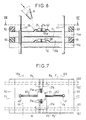
- FIGS. 6 and 7 a method of manufacturing a module according to the invention is now presented, as described with reference to FIGS. 1 to 3.
- a mold of parallelepiped shape (not shown) is provided on a closed bottom from which stands guide means, for example in the form of two elongated rods 40 and 41.
- a first elementary structure of the compact microwave module according to the invention is then formed by introducing into the mold the lower dielectric layer, or substrate, 15a of the elementary structure considered, this layer supporting on its upper face the coplanar inlet and outlet lines 20a and 20b as well as the circuit integrated 20.
- the substrate 15a is provided with two transverse perforations to be guided by the two elongated rods 40 and 41 during its introduction into the mold.
- resin R is deposited on the upper face of the substrate 15a to form the upper layer 15b which covers the coplanar inlet and outlet lines 20a and 20b as well as the circuit integrated 20.
- a second elementary structure of the compact microwave module is then formed by introducing into the mold the lower dielectric layer, or substrate, 14a of this second elementary structure, this lower layer supporting on its upper face the coplanar lines of input and output 21a and 21b as well as the integrated circuit 21.
- Resin R is then deposited on the upper face of the substrate 14a to form the upper layer 14b which covers the coplanar lines of input and output 21a and 21b as well as the integrated circuit 21.
- Spacers 50, 51, respectively 52, 53 arranged laterally can be provided to separate the lower layers 15a, 14a thus successively introduced, thus ensuring a parallel arrangement of the latter.
- the resulting structure is removed from the mold, which is in the form of a parallelepiped.
- this parallelepiped structure defining four lateral faces F1, F2, F3 and F4 is then cut along the cutting planes 100 and 101 parallel and internal respectively to the facing faces F1 and F3, revealing two new faces Fa and Fb.
- On each of these two faces Fa and Fb appear respective ends of the ground conductors and signal conductor of the coplanar lines - input or output - of the various elementary structures.
- These two faces Fa and Fb are then metallized by covering with metal.
- the resulting metallized faces are then etched to form each intermediate connecting line 30 existing between a coplanar inlet line and a coplanar outlet line. This etching is obtained by removing part of the metallized surface on the two faces Fa and Fb.
- the modified parallelepiped structure thus obtained is reintroduced into the mold being guided by the two elongated rods 40 and 41. Resin is injected on the outer sides of the faces Fa and Fb so as to form a remoulded parallelepiped structure of dimension equal to the dimension of the first structure.
- This structure is then removed from the mold to be cut, on the one hand, along cutting planes 102 and 103 parallel and internal respectively to the facing faces F1 and F3, and, on the other hand, along cutting planes 104 and 105 parallel and interiors respectively with the facing faces F4 and F2.
- a final parallelepipedal structure is then obtained defined by the four lateral faces Fc, Fd, Fe and Ff.
- the faces Fc and Fd are naturally external respectively to the faces Fa and Fb on which are written the intermediate coplanar connecting lines 30.
- a ground plane 11, 12 is provided to separate two immediately adjacent modules, for each ground plane, it is planned to attack, typically by laser, the resin on at least one of the faces Fc, Fd, Fe and Ff at points opposite with the edges of this ground plane so as to form an access perforation between the ground plane and the exterior.
- the final structure is then metallized over its entire surface including the access perforations.
- This metallized envelope constitutes a shield for the module, this shield being in electrical connection with the ground planes 11, 12.
- LF low frequency
- wires typically for supplying circuits 20 and 21 are carried by the upper face of the lower layer, or substrate, 14a, 15a on which the integrated circuit 21, 20 is mounted. These wires extend towards the faces Fe and Ff. These faces Fe and Ff, which are metallized as a result of the metallization step described above, are then etched to form each intermediate connecting wire with a LF signal source.
- a row P molding step is intended to cover with resin the etching of the BF wires formed during the row etching step (P-1), a row P laser attack step being intended to form perforations d 'access to this row etching (P-1), and the metallization and etching steps of row P having the aim of producing the desired multilayer BF etching pattern.
Abstract
Description
La présente invention concerne de manière générale un module hyperfréquence ainsi qu'un procédé de fabrication d'un tel module. A titre non limitatif, un tel module est utilisé par exemple pour former l'un d'une pluralité de modules actifs à élément rayonnant d'une antenne active, ces modules étant disposés matriciellement. Le terme "hyperfréquence" est associé dans la suite de la description tant à la plage des ondes centimétriques que des ondes millimétriques.The present invention relates generally to a microwave module and a method of manufacturing such a module. By way of non-limiting example, such a module is used for example to form one of a plurality of active modules with a radiating element of an active antenna, these modules being arranged in a matrix. The term "microwave" is associated in the following description with both the centimeter wave and millimeter wave range.
Le document US-A-5 294 897 propose une structure mono-composant à ligne coplanaire. La structure présentée comprend un substrat diélectrique sur lequel sont montées une portion de ligne coplanaire d'entrée et une portion de ligne coplanaire de sortie respectivement appliquées en entrée et en sortie d'un circuit intégré. Chaque portion de ligne coplanaire - d'entrée et de sortie - comprend une partie supérieure portée par une face supérieure du substrat, une partie intermédiaire traversant le substrat et une partie inférieure portée par le plan de la face inférieure du substrat. Ces parties supérieure, intermédiaire et inférieure prennent la forme générale d'une "marche d'escalier", les deux conducteurs de masse périphériques et le conducteur de masse central de cette partie inférieure de ligne coplanaire étant destinés à être mis en contact avec des bornes correspondantes d'un circuit imprimé. Cette réalisation présente l'inconvénient principal que l'association de plusieurs composants, assurant chacun une fonction donnée, telle qu'amplification, déphasage, etc..., requiert une surface de support importante. En outre, selon cette réalisation, une onde se propage sur ligne coplanaire de composant à composant en traversant un milieu non homogène parfois formé par une couche de substrat, parfois formé par l'air.Document US-A-5,294,897 proposes a single-component structure with a coplanar line. The structure presented comprises a dielectric substrate on which are mounted a portion of input coplanar line and a portion of output coplanar line respectively applied at the input and at the output of an integrated circuit. Each coplanar line portion - inlet and outlet - comprises an upper part carried by an upper face of the substrate, an intermediate part passing through the substrate and a lower part carried by the plane of the lower face of the substrate. These upper, intermediate and lower parts take the general form of a "stair step", the two peripheral earth conductors and the central earth conductor of this lower part of the coplanar line being intended to be brought into contact with terminals corresponding of a printed circuit. This embodiment has the main drawback that the combination of several components, each providing a given function, such as amplification, phase shift, etc., requires a large support surface. In addition, according to this embodiment, a wave propagates on the coplanar line from component to component by passing through a non-homogeneous medium sometimes formed by a layer of substrate, sometimes formed by air.
Pour remédier à l'inconvénient de la surface de support importante requise selon cette première réalisation, il est connu selon la technique antérieure, par exemple rappelée dans le document FR-A-2 697 374, de recourir à un module hyperfréquence compact comprenant une pluralité de structures élémentaires empilées, chaque structure étant constituée par un ou plusieurs circuits intégrés, ou puces, enrobés dans un diélectrique. Dans ce document, une liaison entre deux circuits intégrés appartenant à deux structures respectives distinctes est établie par un fil qui traverse la zone diélectrique séparant ces deux circuits à travers un trou formé dans cette zone. Cette réalisation présente l'inconvénient principal d'une mauvaise propagation d'une onde à fréquence élevée à travers cette liaison filaire.To overcome the drawback of the large support surface required according to this first embodiment, it is known according to the prior art, for example recalled in document FR-A-2 697 374, to use a compact microwave module comprising a plurality of stacked elementary structures, each structure consisting of one or more integrated circuits, or chips, coated in a dielectric. In this document, a connection between two integrated circuits belonging to two respective respective structures is established by a wire which crosses the dielectric zone separating these two circuits through a hole formed in this zone. This embodiment has the main drawback of poor propagation of a wave at high frequency through this wire connection.
L'invention vise donc à remédier aux inconvénients précités en fournissant un module hyperfréquence particulièrement compact et inhibant sensiblement toute perturbation dans les signaux radioélectriques transmis entre circuits.The invention therefore aims to remedy the aforementioned drawbacks by providing a particularly compact microwave module and substantially inhibiting any disturbance in the radio signals transmitted between circuits.
A cette fin, selon une première réalisation de l'invention, un module hyperfréquence comprenant:
- une pluralité de structures élémentaires empilées formant bloc, chaque structure élémentaire comprenant une couche diélectrique inférieure sur une surface supérieure de laquelle est disposé un circuit intégré, et une couche diélectrique supérieure recouvrant le circuit, et
- une ligne de connexion pour connecter un premier circuit intégré monté sur une couche diélectrique d'une première structure parmi ladite pluralité de structures à un second circuit intégré monté sur une couche diélectrique d'une seconde structure parmi ladite pluralité de structures,
- a plurality of stacked elementary structures forming a block, each elementary structure comprising a lower dielectric layer on an upper surface of which an integrated circuit is disposed, and an upper dielectric layer covering the circuit, and
- a connection line for connecting a first integrated circuit mounted on a dielectric layer of a first structure among said plurality of structures to a second integrated circuit mounted on a dielectric layer of a second structure among said plurality of structures,
Typiquement, afin d'assurer un blindage et un bon drain thermique, une structure élémentaire donnée est séparée d'une structure élémentaire immédiatement adjacente par un élément de masse.Typically, in order to provide shielding and a good heat drain, a given elementary structure is separated from an immediately adjacent elementary structure by a ground element.
Dans ce cas, la portion de ligne coplanaire d'entrée et ladite ligne coplanaire de sortie s'étendent toutes deux au-delà d'un plan délimitant chaque rebord respectif du ou des éléments de masse séparant lesdites première et seconde structures élémentaires, de sorte que ladite ligne coplanaire de liaison est distante vers l'extérieur du ou des élément(s) de masse.In this case, the portion of input coplanar line and said output coplanar line both extend beyond a plane delimiting each respective flange of the mass element or elements separating said first and second elementary structures, so that said coplanar connecting line is distant towards the outside of the element (s) of mass.
Un procédé de fabrication d'un tel module comprend les étapes de :
- moulage d'un bloc parallélépipédique comprenant une pluralité de structures élémentaires empilées, chaque structure élémentaire comprenant une couche diélectrique inférieure sur une surface supérieure de laquelle est disposé un circuit intégré et une couche diélectrique supérieure recouvrant le circuit,
- découpe dudit bloc suivant des plans de coupe parallèles et intérieurs respectivement à des faces en regard dudit bloc pour faire apparaître deux nouvelles faces sur chacune desquelles apparaissent des ensembles respectifs d'extrémités de conducteurs de masse et conducteur de signal chacun associé à une ligne coplanaire,
- métallisation desdites deux nouvelles faces, et
- gravure desdites deux nouvelles faces métallisées pour former une ligne coplanaire de liaison reliant des extrémités de conducteurs de masse et conducteur de signal d'une ligne coplanaire d'entrée d'une première structure élémentaire à des extrémités respectives de conducteurs de masse et conducteur de signal d'une ligne coplanaire de sortie d'une seconde structure élémentaire.
- molding of a parallelepipedal block comprising a plurality of stacked elementary structures, each elementary structure comprising a lower dielectric layer on an upper surface of which an integrated circuit is arranged and an upper dielectric layer covering the circuit,
- cutting of said block along parallel and internal cutting planes respectively at opposite faces of said block to reveal two new faces on each of which appear respective sets of ends of ground conductors and signal conductor each associated with a coplanar line,
- metallization of said two new faces, and
- etching of said two new metallized faces to form a coplanar connection line connecting ends of ground conductors and signal conductor of a coplanar input line of a first elementary structure to respective ends of conductors of ground and signal conductor of a coplanar output line of a second elementary structure.
Dans le cas ou des éléments, ou plans, de masse sont prévus pour séparer deux structures élémentaires, le procédé comprend, en outre, les étapes de:
- remoulage du bloc gravé pour recouvrir la ligne coplanaire de liaison d'une enveloppe diélectrique,
- attaque du bloc gravé remoulé sur au moins l'une de ses faces en des points en regard avec les chants des plans de masse, de sorte à former des perforations d'accès entre chaque plan de masse et l'extérieur, et
- blindage du bloc par métallisation totale du bloc, ledit blindage étant en connexion électrique avec les plans de masse à travers lesdites perforations d'accès métallisées.
- re-molding of the engraved block to cover the coplanar connection line with a dielectric envelope,
- attack of the engraved block remolded on at least one of its faces at points opposite with the edges of the ground planes, so as to form access perforations between each ground plane and the outside, and
- shielding of the block by total metallization of the block, said shielding being in electrical connection with the ground planes through said metallized access perforations.
Selon une seconde variante de l'invention, un module compact hyperfréquence comprenant:
- une pluralité de structures élémentaires empilées formant bloc, chaque structure élémentaire comprenant une couche diélectrique inférieure sur une surface supérieure de laquelle est disposé un circuit intégré et une couche diélectrique supérieure recouvrant le circuit, et
- une ligne de connexion pour connecter un premier circuit intégré monté sur une couche diélectrique inférieure d'une première structure parmi ladite pluralité de structures à un second circuit intégré monté sur une couche diélectrique inférieure d'une seconde structure parmi ladite pluralité de structures,
- un élément de masse pour séparer chaque structure élémentaire donnée d'une structure élémentaire immédiatement adjacente, et en ce que
- a plurality of stacked elementary structures forming a block, each elementary structure comprising a lower dielectric layer on an upper surface of which an integrated circuit is disposed and an upper dielectric layer covering the circuit, and
- a connection line for connecting a first integrated circuit mounted on a lower dielectric layer of a first structure among said plurality of structures to a second integrated circuit mounted on a lower dielectric layer of a second structure among said plurality of structures,
- an element of mass to separate each given elementary structure from an immediately adjacent elementary structure, and in that
Avantageusement, ledit au moins un second brin conducteur de masse est en contact avec chaque élément de masse séparant les deux circuits.Advantageously, said at least one second ground conductor strand is in contact with each ground element separating the two circuits.
Ledit au moins un second brin conducteur de masse est par exemple formé par métallisation d'un second trou.Said at least one second ground conductor strand is for example formed by metallization of a second hole.
En outre, les deux conducteurs de masse de chacune des lignes coplanaires d'entrée et de sortie peuvent être reliées entre eux à leurs extrémités respectives par un conducteur de masse additionnel.In addition, the two ground conductors of each of the input and output coplanar lines can be connected to each other at their respective ends by an additional ground conductor.
L'on peut prévoir, une pluralité de seconds brins reliant entre eux les conducteurs de masse et conducteur de masse additionnel de la ligne coplanaire d'entrée et les conducteurs de masse et conducteur de masse additionnel de la ligne coplanaire de sortie, cette pluralité de seconds brins étant disposée en arc de cercle.It is possible to provide, a plurality of second strands connecting together the ground conductors and additional ground conductor of the input coplanar line and the ground conductors and additional ground conductor of the coplanar output line, this plurality of second strands being arranged in an arc.
D'autres caractéristiques et avantages de la présente invention apparaîtront plus clairement à la lecture de la description suivante, en référence aux dessins annexés correspondants, dans lesquels :
- la figure 1 est une vue en perspective d'un module hyperfréquence selon l'invention, dans laquelle est représentée une liaison par ligne coplanaire entre deux circuits intégrés;
- la figure 2 est une vue en coupe transversale du module de la figure 1;
- la figure 3 montre, selon une première variante de l'invention, une vue en perspective détaillée d'une liaison par ligne coplanaire entre deux circuits intégrés appartenant respectivement à deux étages distincts du module;
- la figure 4 montre, selon une seconde variante de l'invention, une vue en perspective détaillée d'une liaison par trou métallisé entre deux circuits intégrés appartenant respectivement à deux étages distincts du module;
- la figure 5 est une vue en coupe de la réalisation de la figure 4;
- la figure 6 est une vue en coupe transversale d'un module selon l'invention en cours de fabrication; et
- la figure 7 est une vue en coupe transversale du module pour illustrer des plans de coupe successifs définis lors cette fabrication pour l'obtention d'un module selon l'invention.
- Figure 1 is a perspective view of a microwave module according to the invention, in which is shown a connection by coplanar line between two integrated circuits;
- Figure 2 is a cross-sectional view of the module of Figure 1;
- FIG. 3 shows, according to a first variant of the invention, a detailed perspective view of a connection by coplanar line between two integrated circuits belonging respectively to two distinct stages of the module;
- FIG. 4 shows, according to a second variant of the invention, a detailed perspective view of a connection by metallized hole between two integrated circuits belonging respectively to two distinct stages of the module;
- Figure 5 is a sectional view of the embodiment of Figure 4;
- Figure 6 is a cross-sectional view of a module according to the invention during manufacture; and
- Figure 7 is a cross-sectional view of the module to illustrate successive sectional planes defined during this manufacture for obtaining a module according to the invention.
En référence aux figures 1 et 2, un module hyperfréquence selon l'invention comprend au moins deux de structures élémentaires empilées qui forment ensemble un bloc. Chaque structure élémentaire comprend un ou plusieurs circuits intégrés, ou puces, 20, 21, 22 qui sont disposés entre deux couches de substrat diélectrique qui forme ensemble une enveloppe diélectrique 15, 14, 13 du ou des circuits intégrés de la structure élémentaire considérée. Ainsi, à titre d'exemple, pour la structure élémentaire incluant le circuit 20, ce circuit 20 est logé dans l'enveloppe diélectrique 15 constitué d'une couche diélectrique inférieure 15a sur une surface supérieure de laquelle est disposé le circuit intégré 20, et d'une couche diélectrique supérieure 15b recouvrant le circuit. En pratique, l'on distingue les couches diélectriques inférieure - 15a, 14a, 13a - et supérieure - 15b, 14b, 13b - de chaque structure élémentaire car elles sont implantées successivement lors de la fabrication du module, comme cela apparaîtra plus clairement dans la suite de la description. Chaque structure élémentaire peut être séparée d'une structure élémentaire immédiatement adjacente par un plan de masse 10, 11, 12. Entre deux structures élémentaires immédiatement adjacentes inférieure et supérieure, le plan de masse 11 est typiquement disposé entre la couche diélectrique inférieure 14a de la structure élémentaire supérieure et la couche diélectrique supérieure 15b de la structure élémentaire inférieure. Dans les figures 1 et 2, le plan de masse 11 sépare la structure élémentaire incluant le composant 20 de la structure élémentaire incluant le composant 21.Referring to Figures 1 and 2, a microwave module according to the invention comprises at least two stacked elementary structures which together form a block. Each elementary structure comprises one or more integrated circuits, or chips, 20, 21, 22 which are arranged between two layers of dielectric substrate which together form a
Il va maintenant être décrit avec plus de détails, selon une première réalisation de l'invention, une liaison par ligne coplanaire entre deux circuits intégrés 20 et 21 appartenant respectivement à deux structures élémentaires. Dans cette liaison par ligne coplanaire, il est supposé que le circuit 20 produit en sortie un signal à appliquer à une entrée du circuit 21. Dans les figures annexées, les deux circuits intégrés 20 et 21 appartiennent respectivement à deux structures élémentaires qui sont immédiatement adjacentes. Néanmoins, l'homme du métier conviendra que les structures élémentaires auxquelles appartiennent les circuits 20 et 21 peuvent être séparées par une ou plusieurs autre(s) structure(s) élémentaire(s).There will now be described in more detail, according to a first embodiment of the invention, a connection by coplanar line between two
En se référant, en outre, à la figure 3, le circuit 21 est monté sur et mis à la masse par un conducteur de masse de support 21c, et est connecté à une ligne coplanaire d'entrée 21a et une ligne coplanaire de sortie 21b. Les conducteur de masse de support 21c, ligne coplanaire d'entrée 21a et ligne coplanaire de sortie 21b sont portés par la couche diélectrique inférieure 14a de la structure élémentaire incluant le circuit 21. La ligne coplanaire d'entrée 21a, respectivement de sortie 21b, comprend deux éléments conducteurs de masse 210a et 212a, respectivement 210b et 212b, encadrant et coplanaires avec un élément conducteur de signal 211a, respectivement 212a. Les deux éléments conducteurs de masse 210a et 212a de la ligne coplanaire d'entrée 21a et les deux éléments conducteurs de masse 210b et 212b de la ligne coplanaire de sortie 21b sont reliés au conducteur de masse de support 21c pour prendre la forme générale d'une structure plane en H. L'élément conducteur de signal 211a est disposé coplanairement entre les deux branches 210a et 212a de la structure plane en H et l'élément conducteur de signal 211b est disposé coplanairement entre les deux branches 210b et 212b de cette structure plane en H. Des extrémités respectives des éléments conducteurs de signal 211a et 211b, en regard avec le conducteur de masse de support 21c, sont connectées avec des supports d'électrode du circuit 21 par des fils courbés 21e et 21s, respectivement. De même, le circuit 20 est monté sur et mis à la masse par un conducteur de masse de support 20c, et est connecté à une ligne coplanaire d'entrée 20b et une ligne coplanaire de sortie 20a. Les conducteur de masse de support 20c, ligne coplanaire d'entrée 20b et ligne coplanaire de sortie 20a sont portés par la couche diélectrique inférieure 15a de la structure élémentaire incluant le circuit 20. La ligne coplanaire d'entrée 20b, respectivement de sortie 20a, comprend deux éléments conducteurs de masse 200b et 202b, respectivement 200a et 202a, encadrant et coplanaires avec un élément conducteur de masse 201b, respectivement 201a. Les deux éléments conducteurs de masse 200b et 202b de la ligne coplanaire d'entrée 20b et les deux éléments conducteurs de masse 200a et 202a de la ligne coplanaire de sortie 20a sont reliés au conducteur de masse de support 20c pour prendre la forme générale d'une structure plane en H. L'élément conducteur de signal 201b est disposé coplanairement entre les deux branches 200b et 202b de la structure plane en H et l'élément conducteur de signal 201a est disposé coplanairement entre les deux branches 200a et 202b de cette structure plane en H. Des extrémités respectives des éléments conducteurs de signal 201b et 201a, en regard avec le conducteur de masse de support 20c, sont connectées avec des supports d'électrode du circuit 20 par des fils courbés 20e et 20s, respectivement.Referring further to Figure 3, the
Une ligne coplanaire intermédiaire de liaison 30, comprenant deux conducteurs de masse 300 et 302, encadrant et coplanaires avec un élément conducteur de signal 301, établit une connexion entre la ligne coplanaire de sortie 20a et la ligne coplanaire d'entrée 21a. Le conducteur de masse 300, respectivement 302, relie une extrémité du conducteur de masse 210a, respectivement 212a, de la ligne coplanaire d'entrée 21a à une extrémité du conducteur de masse 200a, respectivement 202a, de la ligne coplanaire de sortie 20a. Le conducteur de signal 301 relie une extrémité du conducteur de signal 211a de la ligne coplanaire d'entrée 21a à une extrémité du conducteur de signal 201a de la ligne coplanaire de sortie 20a.An intermediate coplanar connecting
Une telle liaison multi-niveaux "tout en ligne coplanaire" entre deux circuits appartenant respectivement à deux structures élémentaires empilées offre une grande compacité du module résultant tout en garantissant une bonne propagation du signal entre les deux circuits 20 et 21. Cette bonne propagation du signal entre les deux circuits 20 et 21 est assurée malgré la disposition perpendiculaire de la ligne coplanaire intermédiaire de liaison 30 par rapport aux lignes coplanaires d'entrée et de sortie 21a et 20a. Cela résulte de la forme des lignes de champ se propageant dans les lignes coplanaires, ces lignes de champ étant sensiblement transversales aux lignes coplanaires. Typiquement, pour une ligne coplanaire, les lignes de champ entre l'un des deux conducteurs de masse et le conducteur de signal et les lignes de champ entre l'autre de ces deux conducteurs de masse et le conducteur de signal sont de sens opposés.Such a multi-level link "all in coplanar line" between two circuits belonging respectively to two stacked elementary structures offers a great compactness of the resulting module while guaranteeing a good propagation of the signal between the two
En pratique, la propagation dans une ligne coplanaire peut ne pas s'effectuer selon ce mode fondamental coplanaire idéal quasi TEM dans lequel les champs électriques s'appliquent entre chaque conducteur de masse et le conducteur de signal. D'autres modes parasites viennent alors s'ajouter qu'il convient d'atténuer, voire d'inhiber, notamment par une géométrie appropriée des lignes coplanaires et une épaisseur de substrat à définir.In practice, propagation in a coplanar line may not take place according to this ideal quasi-TEM coplanar fundamental mode in which the electric fields apply between each ground conductor and the signal conductor. Other parasitic modes are then added which should be attenuated or even inhibited, in particular by an appropriate geometry of the coplanar lines and a thickness of substrate to be defined.
Parmi ces modes parasites, l'on notera notamment le mode "micro ruban" et le mode de volume "à plans parallèles". Le premier de ces modes se caractérise par un champ électrique entre le conducteur de signal, par exemple 211a, et le plan de masse immédiatement inférieur 11, le second de ces modes définissant un champ électrique entre, d'une part, le conducteur de signal et les conducteurs de masse, et, d'autre part, le plan de masse immédiatement inférieur. Le premier de ces modes peut être atténué en choisissant une largeur du conducteur de signal 211a bien inférieure à l'épaisseur du substrat, ou couche inférieure 14a. L'on peut également choisir une largeur de fente entre conducteur de masse et conducteur de signal faible par rapport à l'épaisseur de la ligne coplanaire. L'on peut encore utiliser un substrat d'épaisseur relativement élevée, typiquement de l'ordre de 400 µm, sans que cette épaisseur soit trop importante car donnant naissance à un mode de type rectangulaire de type TE.Among these parasitic modes, one will note in particular the "micro ribbon" mode and the "parallel planes" volume mode. The first of these modes is characterized by an electric field between the signal conductor, for example 211a, and the immediately
Comme montré dans la figure 3, dans le cas où un plan de masse 11 est prévu entre chaque structure élémentaire, la ligne coplanaire d'entrée 21a et la ligne coplanaire de sortie 20a s'étendent toutes deux au-delà d'un plan délimitant chaque rebord respectif du ou des éléments de masse séparant les structures élémentaires auxquelles appartiennent respectivement les circuits 20 et 21, de sorte que la ligne coplanaire de liaison est distante vers l'extérieur du ou des élément(s)) de masse séparant les deux structures considérées.As shown in FIG. 3, in the case where a
Avantageusement, dans tous les cas, la ligne coplanaire de liaison 30 est de préférence intégrée dans le module en étant recouverte d'une couche diélectrique, de sorte à éviter toute désadaptation électrique résultant de la propagation du signal dans des milieux, à savoir substrat et air, de permittivités respectives différentes.Advantageously, in all cases, the coplanar connecting
En référence aux figures 4 et 5, il est maintenant décrit une seconde réalisation de l'invention. Au même titre que dans la variante précédente, le circuit 21 est monté sur et mis à la masse par un conducteur de masse de support 21c, et est connecté à une ligne coplanaire d'entrée 21a et une ligne coplanaire de sortie 21b. Les conducteur de masse de support 21c, ligne coplanaire d'entrée 21a et ligne coplanaire de sortie 21b sont portés par la couche diélectrique inférieure 14a de la structure élémentaire incluant le circuit 21. La portion de ligne coplanaire d'entrée 21a, respectivement de sortie 21b, comprend deux éléments conducteurs de masse 210a et 212a, respectivement 210b et 212b, encadrant et coplanaires avec un élément conducteur de masse 211a, respectivement 212a. Les deux éléments conducteurs de masse 210a et 212a de la ligne coplanaire d'entrée 21a et les deux éléments conducteurs de masse 210b et 212b de la ligne coplanaire de sortie 21b sont reliés au conducteur de masse de support 21c pour prendre la forme générale d'une structure plane en H. L'élément conducteur de signal 211a est disposé coplanairement entre les deux branches 210a et 212a de la structure plane en H et l'élément conducteur de signal 211b est disposé coplanairement entre les deux branches 210b et 212b de cette structure plane en H. Des extrémités respectives des éléments conducteurs de signal 211a et 211b, en regard avec le conducteur de masse de support 21c, sont connectées avec des supports d'électrode du circuit 21 par des fils courbés 21e et 21s, respectivement. Par ailleurs, le circuit 20 est monté sur et mis à la masse par un conducteur de masse de support 20c, et est connecté à une ligne coplanaire d'entrée 20b et une ligne coplanaire de sortie 20a. Les conducteur de masse de support 20c, ligne coplanaire d'entrée 20b et ligne coplanaire de sortie 20a sont portés par la couche diélectrique inférieure 15a de la structure élémentaire incluant le circuit 20. La ligne coplanaire d'entrée 20b, respectivement de sortie 20a, comprend deux éléments conducteurs de masse 200b et 202b, respectivement 200a et 202a, encadrant et coplanaires avec un élément conducteur de masse 201b, respectivement 201a. Les deux éléments conducteurs de masse 200b et 202b de la ligne coplanaire d'entrée 20b et les deux éléments conducteurs de masse 200a et 202a de la ligne coplanaire de sortie 20a sont reliés au conducteur de masse de support 20c pour prendre la forme générale d'une structure plane en H. L'élément conducteur de signal 201b est disposé coplanairement entre les deux branches 200b et 202b de la structure plane en H et l'élément conducteur de signal 201a est disposé coplanairement entre les deux branches 200a et 202b de cette structure plane en H. Des extrémités respectives des éléments conducteurs de signal 201b et 201a, en regard avec le conducteur de masse de support 20c, sont connectées avec des supports d'électrode du circuit 20 par des fils courbés 20e et 20s, respectivement. Dans cette seconde variante, chaque structure élémentaire donnée est séparée d'une structure élémentaire immédiatement adjacente par un plan de masse 11. Avantageusement, les deux conducteurs de masse 210a et 212a de la ligne coplanaire d'entrée 21a sont reliées entre eux à leurs extrémités respectives par un conducteur de masse additionnel 213a disposé perpendiculairement aux conducteurs de masse, et les deux conducteurs de masse 200a et 202a de la ligne coplanaire de sortie 20a sont reliées entre eux à leurs extrémités respectives par un conducteur de masse additionnel 203a.With reference to FIGS. 4 and 5, a second embodiment of the invention is now described. As in the previous variant, the
Dans cette seconde variante, la liaison entre la ligne coplanaire de sortie 20a et la ligne coplanaire d'entrée 21a est assurée par, d'une part, un premier brin conducteur de signal 311 reliant le conducteur de signal 211a de la ligne coplanaire d'entrée 21a et le conducteur de signal 201a de la ligne coplanaire de sortie 20a à travers un trou H traversant chaque couche diélectrique inférieure et supérieure ainsi que chaque plan de masse 11 séparant les deux circuits 20 et 21, et, d'autre part, au moins un second brin conducteur de masse 310, 312 reliant au moins l'un des conducteurs de masse 210a, 212a de la ligne coplanaire d'entrée 21a à au moins l'un des conducteurs de masse 200A, 202a de la ligne coplanaire de sortie 21a à travers un trou traversant chaque couche diélectrique inférieure et supérieure ainsi que chaque élément de masse séparant les deux circuits 20 et 21.In this second variant, the connection between the
Typiquement, chacun des seconds brins conducteurs de masse 310, 312 est formé par métallisation de trou. Ainsi, le brin métallisé occupe la totalité du trou qu'il traverse. En outre, afin d'assurer une parfaite homogénéité des potentiels de masse, chacun des seconds brins conducteurs de masse 310, 312 est en contact avec chaque plan de masse qui séparent les deux circuits 20 et 21. Selon une variante, un second brin de masse est constitué d'une pluralité de portions de brins. Si N désigne le nombre de plans de masse séparant les deux circuits 20 et 21, (N+1) portions de brins de masse sont prévues. Par rapport à un plan de masse donné, les extrémités de deux des (N+1) portions de brins de masse sont fixés en regard de part et d'autre du plan de masse.Typically, each of the second
Dans la figure 4, seuls deux brins conducteurs de masse 310 et 312 sont représentés. Néanmoins, comme montré dans la figure 5, de manière tout à fait avantageuse, plusieurs seconds brins 310, 312, 313 et 314 peuvent être utilisés pour relier entre eux les conducteurs de masse 200a, 202a et conducteur de masse additionnel 203a de la ligne coplanaire de sortie 20a et lesdits conducteurs de masse 210a, 212a et conducteur de masse additionnel 213a de la ligne coplanaire d'entrée 21a. Au niveau d'une ligne coplanaire, telle que 21a, des extrémités respectives de ces seconds brins viennent au contact de la surface inférieure des conducteurs de masse 210a, 212a et conducteur de masse additionnel 213a de la ligne coplanaire d'entrée 21a, ces points de contact définissant par exemple un arc de cercle. En pratique toute autre disposition peut être utilisée, en prévoyant plusieurs seconds brins entourant au moins partiellement le brin conducteur de signal 311. Cette alternative offre une propagation du signal entre ligne coplanaire de sortie 20a et ligne coplanaire d'entrée 21a de type ligne coaxiale, en raison de la disposition "périphérique" des seconds brins conducteurs de masse 310, 312, 313 et 314 autour du brin conducteur de signal 311.In Figure 4, only two
En référence aux figures 6 et 7, il est maintenant présenté un procédé de fabrication d'un module selon l'invention, tel que décrit en référence aux figures 1 à 3.With reference to FIGS. 6 and 7, a method of manufacturing a module according to the invention is now presented, as described with reference to FIGS. 1 to 3.
Pour ce procédé, il est prévu un moule de forme parallélépipédique (non représenté) sur un fond obturé duquel se dresse des moyens de guidage, par exemple sous la forme de deux tiges allongées 40 et 41. Une première structure élémentaire du module hyperfréquence compact selon l'invention est alors formée par introduction dans le moule de la couche diélectrique inférieure, ou substrat, 15a de la structure élémentaire considérée, cette couche supportant sur sa face supérieure les lignes coplanaires d'entrée et de sortie 20a et 20b ainsi que le circuit intégré 20. Le substrat 15a est muni de deux perforations transversales pour être guidé par les deux tiges allongées 40 et 41 lors de son introduction dans le moule. Puis de la résine R est déposée sur la face supérieure du substrat 15a pour former la couche supérieure 15b qui recouvre les lignes coplanaires d'entrée et de sortie 20a et 20b ainsi que le circuit intégré 20. Ensuite, une seconde structure élémentaire du module hyperfréquence compact est alors formée par introduction dans le moule de la couche diélectrique inférieure, ou substrat, 14a de cette seconde structure élémentaire, cette couche inférieure supportant sur sa face supérieure les lignes coplanaires d'entrée et de sortie 21a et 21b ainsi que le circuit intégré 21. De la résine R est alors déposée sur la face supérieure du substrat 14a pour former la couche supérieure 14b qui recouvre les lignes coplanaires d'entrée et de sortie 21a et 21b ainsi que le circuit intégré 21. Par réitération de ces opérations, une pluralité de structures élémentaires peuvent ainsi être empilées. Des entretoises 50, 51, respectivement 52, 53 disposées latéralement peuvent être prévues pour séparer les couches inférieures 15a, 14a ainsi successivement introduites, assurant ainsi une disposition parallèle de ces dernières. Après empilement du nombre souhaité de structures élémentaires, l'on démoule la structure résultante qui se présente sous la forme d'un parallélépipède.For this process, a mold of parallelepiped shape (not shown) is provided on a closed bottom from which stands guide means, for example in the form of two
En référence à la figure 7, cette structure parallélépipédique définissant quatre faces latérales F1, F2, F3 et F4 est ensuite découpée suivant les plans de coupe 100 et 101 parallèles et intérieurs respectivement aux faces en regard F1 et F3, faisant apparaître deux nouvelles faces Fa et Fb. Sur chacune ces deux faces Fa et Fb, apparaissent des extrémités respectives des conducteurs de masse et conducteur de signal des lignes coplanaires - d'entrée ou de sortie - des différentes structures élémentaires. Ces deux faces Fa et Fb sont alors métallisées par recouvrement de métal. Les faces métallisées résultantes sont ensuite gravées pour former chaque ligne intermédiaire de liaison 30 existante entre une ligne coplanaire d'entrée et une ligne coplanaire de sortie. Cette gravure est obtenue par suppression d'une partie de la surface métallisée sur les deux faces Fa et Fb.With reference to FIG. 7, this parallelepiped structure defining four lateral faces F1, F2, F3 and F4 is then cut along the cutting
La structure parallélépipédique modifiée ainsi obtenue est réintroduite dans le moule en étant guidée par les deux tiges allongées 40 et 41. De la résine est injectée sur les côtés extérieurs des faces Fa et Fb de sorte à former une structure parallélépipédique remoulée de dimension égale à la dimension de la première structure. Cette structure est alors démoulée pour être découpée, d'une part, suivant des plans de coupe 102 et 103 parallèles et intérieurs respectivement aux faces en regard F1 et F3, et, d'autre part, suivant des plans de coupe 104 et 105 parallèles et intérieurs respectivement aux faces en regard F4 et F2. Est alors obtenue une structure parallélépipédique finale définie par les quatre faces latérales Fc, Fd, Fe et Ff. Les faces Fc et Fd sont naturellement extérieures respectivement aux faces Fa et Fb sur lesquelles sont inscrites les lignes coplanaires intermédiaires de liaison 30. Lorsqu'un plan de masse 11, 12 est prévu pour séparer deux modules immédiatement adjacents, pour chaque plan de masse, il est prévu d'attaquer, typiquement par laser, la résine sur au moins l'une des faces Fc, Fd, Fe et Ff en des points en regard avec les chants de ce plan de masse de sorte à former une perforation d'accès entre le plan de masse et l'extérieur. La structure finale est ensuite métallisée sur toute sa surface en incluant les perforations d'accès. Cette enveloppe métallisée constitue un blindage du module, ce blindage étant en connexion électrique avec les plan de masse 11, 12.The modified parallelepiped structure thus obtained is reintroduced into the mold being guided by the two
Il n'a pas été fait mention jusqu'à présent des fils basse fréquence, ou BF, typiquement d'alimentation des circuits 20 et 21. Comme montré dans la figure 7, pour chaque structure élémentaire, ces fils 60, 61 sont portés par la face supérieure de la couche inférieure, ou substrat, 14a, 15a sur laquelle est monté le circuit intégré 21, 20. Ces fils s'étendent vers les faces Fe et Ff. Ces faces Fe et Ff, qui sont métallisées en résultat de l'étape de métallisation décrite ci-dessus, sont alors gravées pour former chaque fil intermédiaire de liaison avec une source de signal BF.Hitherto, no mention has been made of low frequency, or LF, wires typically for supplying
En pratique, il est possible d'étendre ce qui vient décrit à une réalisation par fils basse fréquence multicouches. Dans ce cas, sont prévues des étapes itératives de moulage, attaque laser, métallisation de la face concernée et gravure. Une étape de moulage de rang P est destinée à recouvrir de résine la gravure des fils BF formée lors de l'étape de gravure de rang (P-1), une étape d'attaque laser de rang P étant destinée à former des perforations d'accès à cette gravure de rang (P-1), et les étape de métallisation et gravure de rang P ayant pour but de réaliser le motif multicouche de gravure BF souhaité.In practice, it is possible to extend what has just been described to an embodiment using multilayer low frequency wires. In this case, iterative molding steps, laser attack, metallization of the face concerned and etching are provided. A row P molding step is intended to cover with resin the etching of the BF wires formed during the row etching step (P-1), a row P laser attack step being intended to form perforations d 'access to this row etching (P-1), and the metallization and etching steps of row P having the aim of producing the desired multilayer BF etching pattern.
Claims (14)
Applications Claiming Priority (2)
| Application Number | Priority Date | Filing Date | Title |
|---|---|---|---|
| FR9604249 | 1996-04-04 | ||
| FR9604249A FR2747239B1 (en) | 1996-04-04 | 1996-04-04 | COMPACT MICROWAVE MODULE |
Publications (2)
| Publication Number | Publication Date |
|---|---|
| EP0800210A1 true EP0800210A1 (en) | 1997-10-08 |
| EP0800210B1 EP0800210B1 (en) | 2002-09-04 |
Family
ID=9490914
Family Applications (1)
| Application Number | Title | Priority Date | Filing Date |
|---|---|---|---|
| EP97400698A Expired - Lifetime EP0800210B1 (en) | 1996-04-04 | 1997-03-27 | Compact microwave module |
Country Status (5)
| Country | Link |
|---|---|
| US (1) | US5917388A (en) |
| EP (1) | EP0800210B1 (en) |
| CA (1) | CA2201771A1 (en) |
| DE (1) | DE69715072T2 (en) |
| FR (1) | FR2747239B1 (en) |
Cited By (3)
| Publication number | Priority date | Publication date | Assignee | Title |
|---|---|---|---|---|
| EP1069639A2 (en) * | 1999-06-29 | 2001-01-17 | Mitsubishi Denki Kabushiki Kaisha | Radio-frequency circuit module |
| EP1176661A1 (en) * | 2000-03-09 | 2002-01-30 | Lucent Technologies Inc. | Resonant capacitive coupler |
| EP1597791A2 (en) * | 2003-02-19 | 2005-11-23 | Electro-Tec Corp. | Broadband high-frequency slip ring system |
Families Citing this family (21)
| Publication number | Priority date | Publication date | Assignee | Title |
|---|---|---|---|---|
| FR2759527B1 (en) * | 1997-02-10 | 2002-07-19 | Alsthom Cge Alkatel | MONOBLOCK STRUCTURE OF STACKED COMPONENTS |
| US7321485B2 (en) | 1997-04-08 | 2008-01-22 | X2Y Attenuators, Llc | Arrangement for energy conditioning |
| US7301748B2 (en) | 1997-04-08 | 2007-11-27 | Anthony Anthony A | Universal energy conditioning interposer with circuit architecture |
| US7336468B2 (en) | 1997-04-08 | 2008-02-26 | X2Y Attenuators, Llc | Arrangement for energy conditioning |
| US9054094B2 (en) | 1997-04-08 | 2015-06-09 | X2Y Attenuators, Llc | Energy conditioning circuit arrangement for integrated circuit |
| JP2000195720A (en) * | 1998-10-22 | 2000-07-14 | Taiyo Yuden Co Ltd | Laminated electronic component |
| US6882239B2 (en) * | 2001-05-08 | 2005-04-19 | Formfactor, Inc. | Electromagnetically coupled interconnect system |
| KR100435813B1 (en) * | 2001-12-06 | 2004-06-12 | 삼성전자주식회사 | Multi chip package using metal bar and manufacturing method thereof |
| WO2004044982A1 (en) * | 2002-11-12 | 2004-05-27 | Fujitsu Limited | Packaging structure |
| US7675729B2 (en) | 2003-12-22 | 2010-03-09 | X2Y Attenuators, Llc | Internally shielded energy conditioner |
| US7466157B2 (en) * | 2004-02-05 | 2008-12-16 | Formfactor, Inc. | Contactless interfacing of test signals with a device under test |
| US7187256B2 (en) * | 2004-02-19 | 2007-03-06 | Hittite Microwave Corporation | RF package |
| KR100618378B1 (en) * | 2005-02-25 | 2006-08-31 | 삼성전자주식회사 | Apparatus for wideband transmission conversion from CWP to parallel transmission line |
| WO2006093831A2 (en) | 2005-03-01 | 2006-09-08 | X2Y Attenuators, Llc | Energy conditioner with tied through electrodes |
| JP2008535207A (en) | 2005-03-01 | 2008-08-28 | エックストゥーワイ アテニュエイターズ,エルエルシー | Regulator with coplanar conductor |
| CN101395683A (en) | 2006-03-07 | 2009-03-25 | X2Y衰减器有限公司 | Energy conditioner structures |
| US7851709B2 (en) * | 2006-03-22 | 2010-12-14 | Advanced Semiconductor Engineering, Inc. | Multi-layer circuit board having ground shielding walls |
| US9000851B1 (en) * | 2011-07-14 | 2015-04-07 | Hittite Microwave Corporation | Cavity resonators integrated on MMIC and oscillators incorporating the same |
| US9123983B1 (en) | 2012-07-20 | 2015-09-01 | Hittite Microwave Corporation | Tunable bandpass filter integrated circuit |
| JP6222747B2 (en) * | 2015-08-26 | 2017-11-01 | Necスペーステクノロジー株式会社 | Circuit structure |
| DE102018105349A1 (en) | 2018-03-08 | 2019-09-12 | Infineon Technologies Ag | Device with at least one strip conductor |
Citations (4)
| Publication number | Priority date | Publication date | Assignee | Title |
|---|---|---|---|---|
| US4899118A (en) * | 1988-12-27 | 1990-02-06 | Hughes Aircraft Company | Low temperature cofired ceramic packages for microwave and millimeter wave gallium arsenide integrated circuits |
| US5294897A (en) * | 1992-07-20 | 1994-03-15 | Mitsubishi Denki Kabushiki Kaisha | Microwave IC package |
| FR2697374A1 (en) * | 1992-10-28 | 1994-04-29 | Ball Corp | Multilayer microstrip assembly and method of manufacture |
| US5406125A (en) * | 1993-04-15 | 1995-04-11 | Martin Marietta Corp. | Semiconductor device having a metalized via hole |
Family Cites Families (7)
| Publication number | Priority date | Publication date | Assignee | Title |
|---|---|---|---|---|
| US3303439A (en) * | 1965-06-14 | 1967-02-07 | Western Electric Co | Strip transmission line interboard connection |
| US5057798A (en) * | 1990-06-22 | 1991-10-15 | Hughes Aircraft Company | Space-saving two-sided microwave circuitry for hybrid circuits |
| US5376561A (en) * | 1990-12-31 | 1994-12-27 | Kopin Corporation | High density electronic circuit modules |
| US5768109A (en) * | 1991-06-26 | 1998-06-16 | Hughes Electronics | Multi-layer circuit board and semiconductor flip chip connection |
| US5545924A (en) * | 1993-08-05 | 1996-08-13 | Honeywell Inc. | Three dimensional package for monolithic microwave/millimeterwave integrated circuits |
| US5644277A (en) * | 1995-02-27 | 1997-07-01 | Hughes Aircraft Company | Three-wire-line vertical interconnect structure for multilevel substrates |
| US5689216A (en) * | 1996-04-01 | 1997-11-18 | Hughes Electronics | Direct three-wire to stripline connection |
-
1996
- 1996-04-04 FR FR9604249A patent/FR2747239B1/en not_active Expired - Fee Related
-
1997
- 1997-03-27 DE DE69715072T patent/DE69715072T2/en not_active Expired - Fee Related
- 1997-03-27 EP EP97400698A patent/EP0800210B1/en not_active Expired - Lifetime
- 1997-04-03 CA CA002201771A patent/CA2201771A1/en not_active Abandoned
- 1997-04-03 US US08/825,956 patent/US5917388A/en not_active Expired - Fee Related
Patent Citations (4)
| Publication number | Priority date | Publication date | Assignee | Title |
|---|---|---|---|---|
| US4899118A (en) * | 1988-12-27 | 1990-02-06 | Hughes Aircraft Company | Low temperature cofired ceramic packages for microwave and millimeter wave gallium arsenide integrated circuits |
| US5294897A (en) * | 1992-07-20 | 1994-03-15 | Mitsubishi Denki Kabushiki Kaisha | Microwave IC package |
| FR2697374A1 (en) * | 1992-10-28 | 1994-04-29 | Ball Corp | Multilayer microstrip assembly and method of manufacture |
| US5406125A (en) * | 1993-04-15 | 1995-04-11 | Martin Marietta Corp. | Semiconductor device having a metalized via hole |
Cited By (6)
| Publication number | Priority date | Publication date | Assignee | Title |
|---|---|---|---|---|
| EP1069639A2 (en) * | 1999-06-29 | 2001-01-17 | Mitsubishi Denki Kabushiki Kaisha | Radio-frequency circuit module |
| EP1069639A3 (en) * | 1999-06-29 | 2002-05-22 | Mitsubishi Denki Kabushiki Kaisha | Radio-frequency circuit module |
| EP1484815A1 (en) * | 1999-06-29 | 2004-12-08 | Mitsubishi Denki Kabushiki Kaisha | Radio-frequency circuit module |
| EP1176661A1 (en) * | 2000-03-09 | 2002-01-30 | Lucent Technologies Inc. | Resonant capacitive coupler |
| EP1597791A2 (en) * | 2003-02-19 | 2005-11-23 | Electro-Tec Corp. | Broadband high-frequency slip ring system |
| EP1597791A4 (en) * | 2003-02-19 | 2007-10-10 | Moog Inc | Broadband high-frequency slip ring system |
Also Published As
| Publication number | Publication date |
|---|---|
| CA2201771A1 (en) | 1997-10-04 |
| FR2747239A1 (en) | 1997-10-10 |
| DE69715072T2 (en) | 2003-05-22 |
| US5917388A (en) | 1999-06-29 |
| EP0800210B1 (en) | 2002-09-04 |
| DE69715072D1 (en) | 2002-10-10 |
| FR2747239B1 (en) | 1998-05-15 |
Similar Documents
| Publication | Publication Date | Title |
|---|---|---|
| EP0800210B1 (en) | Compact microwave module | |
| EP2510574B1 (en) | Microwave transition device between a microstrip line and a rectangular waveguide | |
| EP0481417B1 (en) | Device for feeding an antenna element radiating two orthogonal polarisations | |
| EP0044779B1 (en) | Folded dipoles in tri-plate technology for very high frequencies, and arrays comprising the same | |
| EP0064313B1 (en) | Circularly polarised microwave radiating element and flat microwave antenna using an array of such elements | |
| FR2772517A1 (en) | MULTI-FREQUENCY ANTENNA MADE ACCORDING TO MICRO-TAPE TECHNIQUE AND DEVICE INCLUDING THIS ANTENNA | |
| EP0310463A1 (en) | Housing for a high-density integrated circuit | |
| EP2136401A1 (en) | Process and apparatus for tri-dimensional interconnection of electronic devices | |
| FR2778024A1 (en) | Connection structure for lines of dielectric waveguides used for high frequency signal transmission in the microwave frequency | |
| EP0048195A1 (en) | Microwave directional coupler between rectangular waveguide and triplate strip line | |
| EP1617503A1 (en) | Frequency filter and its method of realization | |
| FR2754108A1 (en) | TRANSITION BETWEEN A CRETE WAVEGUIDE AND A PLANAR CIRCUIT | |
| EP0387955A1 (en) | Package for hyperfrequency integrated circuit | |
| FR2991108A1 (en) | BLINDED COPLANAR LINE | |
| EP2432072B1 (en) | Wideband balun on a multilayer circuit for a network antenna | |
| EP0983616B1 (en) | Method and device for connecting two millimetric elements | |
| EP3047535A1 (en) | Junction device between a printed transmission line and a dielectric waveguide | |
| EP3537542B1 (en) | Three-dimensional antenna | |
| EP3631893A1 (en) | Implementation of inductive posts in an siw structure and production of a generic filter | |
| EP3537541B1 (en) | Electromagnetic decoupling | |
| FR2958085A1 (en) | TUNABLE HIGH FREQUENCY TRANSMISSION LINE | |
| EP0557176B1 (en) | Feeding device for a plate antenna with two crossed polarizations and array equipped with such a device | |
| EP3537540A1 (en) | Electromagnetic decoupling | |
| WO2004049455A1 (en) | Pin diodes which are made from polycrystalline heterostructure materials, phase-shifting panel and antenna comprising pin diodes | |
| FR2628569A1 (en) | Hyperfrequency switching IC mfr. on silicon substrate - covering water dielectric layers which are etched off at selected locations to define islands separated by glass-filled recesses |
Legal Events
| Date | Code | Title | Description |
|---|---|---|---|
| PUAI | Public reference made under article 153(3) epc to a published international application that has entered the european phase |
Free format text: ORIGINAL CODE: 0009012 |
|
| AK | Designated contracting states |
Kind code of ref document: A1 Designated state(s): DE ES FI GB IT SE |
|
| 17P | Request for examination filed |
Effective date: 19980228 |
|
| RAP1 | Party data changed (applicant data changed or rights of an application transferred) |
Owner name: ALCATEL SPACE INDUSTRIES |
|
| 17Q | First examination report despatched |
Effective date: 19990924 |
|
| GRAG | Despatch of communication of intention to grant |
Free format text: ORIGINAL CODE: EPIDOS AGRA |
|
| GRAG | Despatch of communication of intention to grant |
Free format text: ORIGINAL CODE: EPIDOS AGRA |
|
| GRAH | Despatch of communication of intention to grant a patent |
Free format text: ORIGINAL CODE: EPIDOS IGRA |
|
| GRAH | Despatch of communication of intention to grant a patent |
Free format text: ORIGINAL CODE: EPIDOS IGRA |
|
| GRAA | (expected) grant |
Free format text: ORIGINAL CODE: 0009210 |
|
| AK | Designated contracting states |
Kind code of ref document: B1 Designated state(s): DE ES FI GB IT SE |
|
| PG25 | Lapsed in a contracting state [announced via postgrant information from national office to epo] |
Ref country code: FI Free format text: LAPSE BECAUSE OF FAILURE TO SUBMIT A TRANSLATION OF THE DESCRIPTION OR TO PAY THE FEE WITHIN THE PRESCRIBED TIME-LIMIT Effective date: 20020904 |
|
| REG | Reference to a national code |
Ref country code: GB Ref legal event code: FG4D Free format text: NOT ENGLISH |
|
| GBT | Gb: translation of ep patent filed (gb section 77(6)(a)/1977) |
Effective date: 20020904 |
|
| REF | Corresponds to: |
Ref document number: 69715072 Country of ref document: DE Date of ref document: 20021010 |
|
| PG25 | Lapsed in a contracting state [announced via postgrant information from national office to epo] |
Ref country code: SE Free format text: LAPSE BECAUSE OF FAILURE TO SUBMIT A TRANSLATION OF THE DESCRIPTION OR TO PAY THE FEE WITHIN THE PRESCRIBED TIME-LIMIT Effective date: 20021204 |
|
| RAP2 | Party data changed (patent owner data changed or rights of a patent transferred) |
Owner name: ALCATEL |
|
| PGFP | Annual fee paid to national office [announced via postgrant information from national office to epo] |
Ref country code: GB Payment date: 20030226 Year of fee payment: 7 |
|
| PGFP | Annual fee paid to national office [announced via postgrant information from national office to epo] |
Ref country code: DE Payment date: 20030311 Year of fee payment: 7 |
|
| PG25 | Lapsed in a contracting state [announced via postgrant information from national office to epo] |
Ref country code: ES Free format text: LAPSE BECAUSE OF FAILURE TO SUBMIT A TRANSLATION OF THE DESCRIPTION OR TO PAY THE FEE WITHIN THE PRESCRIBED TIME-LIMIT Effective date: 20030328 |
|
| PLBE | No opposition filed within time limit |
Free format text: ORIGINAL CODE: 0009261 |
|
| STAA | Information on the status of an ep patent application or granted ep patent |
Free format text: STATUS: NO OPPOSITION FILED WITHIN TIME LIMIT |
|
| 26N | No opposition filed |
Effective date: 20030605 |
|
| PG25 | Lapsed in a contracting state [announced via postgrant information from national office to epo] |
Ref country code: GB Free format text: LAPSE BECAUSE OF NON-PAYMENT OF DUE FEES Effective date: 20040327 |
|
| PG25 | Lapsed in a contracting state [announced via postgrant information from national office to epo] |
Ref country code: DE Free format text: LAPSE BECAUSE OF NON-PAYMENT OF DUE FEES Effective date: 20041001 |
|
| GBPC | Gb: european patent ceased through non-payment of renewal fee |
Effective date: 20040327 |
|
| PG25 | Lapsed in a contracting state [announced via postgrant information from national office to epo] |
Ref country code: IT Free format text: LAPSE BECAUSE OF NON-PAYMENT OF DUE FEES Effective date: 20050327 |