EP0802625A1 - Unbalanced fet mixer - Google Patents
Unbalanced fet mixer Download PDFInfo
- Publication number
- EP0802625A1 EP0802625A1 EP96302777A EP96302777A EP0802625A1 EP 0802625 A1 EP0802625 A1 EP 0802625A1 EP 96302777 A EP96302777 A EP 96302777A EP 96302777 A EP96302777 A EP 96302777A EP 0802625 A1 EP0802625 A1 EP 0802625A1
- Authority
- EP
- European Patent Office
- Prior art keywords
- mixer
- port
- input
- signal
- transistor
- Prior art date
- Legal status (The legal status is an assumption and is not a legal conclusion. Google has not performed a legal analysis and makes no representation as to the accuracy of the status listed.)
- Granted
Links
- 238000002955 isolation Methods 0.000 claims abstract description 21
- 230000001939 inductive effect Effects 0.000 claims abstract description 12
- 230000008878 coupling Effects 0.000 claims abstract description 8
- 238000010168 coupling process Methods 0.000 claims abstract description 8
- 238000005859 coupling reaction Methods 0.000 claims abstract description 8
- 230000002265 prevention Effects 0.000 claims 3
- 239000003990 capacitor Substances 0.000 description 8
- 238000010586 diagram Methods 0.000 description 6
- 230000008901 benefit Effects 0.000 description 5
- 230000005669 field effect Effects 0.000 description 4
- 230000004075 alteration Effects 0.000 description 2
- 230000001965 increasing effect Effects 0.000 description 2
- 230000004048 modification Effects 0.000 description 2
- 238000012986 modification Methods 0.000 description 2
- 229910001218 Gallium arsenide Inorganic materials 0.000 description 1
- 230000005540 biological transmission Effects 0.000 description 1
- 230000000903 blocking effect Effects 0.000 description 1
- 230000015556 catabolic process Effects 0.000 description 1
- 238000012512 characterization method Methods 0.000 description 1
- 238000006243 chemical reaction Methods 0.000 description 1
- 230000006835 compression Effects 0.000 description 1
- 238000007906 compression Methods 0.000 description 1
- 230000002349 favourable effect Effects 0.000 description 1
- 238000000034 method Methods 0.000 description 1
- 235000014366 other mixer Nutrition 0.000 description 1
- 238000005086 pumping Methods 0.000 description 1
Images


Classifications
-
- H—ELECTRICITY
- H03—ELECTRONIC CIRCUITRY
- H03D—DEMODULATION OR TRANSFERENCE OF MODULATION FROM ONE CARRIER TO ANOTHER
- H03D9/00—Demodulation or transference of modulation of modulated electromagnetic waves
- H03D9/06—Transference of modulation using distributed inductance and capacitance
- H03D9/0658—Transference of modulation using distributed inductance and capacitance by means of semiconductor devices having more than two electrodes
- H03D9/0675—Transference of modulation using distributed inductance and capacitance by means of semiconductor devices having more than two electrodes using field effect transistors
-
- H—ELECTRICITY
- H03—ELECTRONIC CIRCUITRY
- H03D—DEMODULATION OR TRANSFERENCE OF MODULATION FROM ONE CARRIER TO ANOTHER
- H03D2200/00—Indexing scheme relating to details of demodulation or transference of modulation from one carrier to another covered by H03D
- H03D2200/0041—Functional aspects of demodulators
- H03D2200/0088—Reduction of intermodulation, nonlinearities, adjacent channel interference; intercept points of harmonics or intermodulation products
-
- H—ELECTRICITY
- H03—ELECTRONIC CIRCUITRY
- H03D—DEMODULATION OR TRANSFERENCE OF MODULATION FROM ONE CARRIER TO ANOTHER
- H03D2200/00—Indexing scheme relating to details of demodulation or transference of modulation from one carrier to another covered by H03D
- H03D2200/0041—Functional aspects of demodulators
- H03D2200/009—Reduction of local oscillator or RF leakage
-
- H—ELECTRICITY
- H03—ELECTRONIC CIRCUITRY
- H03D—DEMODULATION OR TRANSFERENCE OF MODULATION FROM ONE CARRIER TO ANOTHER
- H03D7/00—Transference of modulation from one carrier to another, e.g. frequency-changing
- H03D7/12—Transference of modulation from one carrier to another, e.g. frequency-changing by means of semiconductor devices having more than two electrodes
- H03D7/125—Transference of modulation from one carrier to another, e.g. frequency-changing by means of semiconductor devices having more than two electrodes with field effect transistors
Definitions
- This invention relates generally to radio frequency mixers, and more particularly to mixers requiring reduced local oscillator drive levels and having high third order intercepts.
- the dynamic range of many prior art microwave front-ends is controlled by the single and two-tone intermodulation levels of the mixers therein.
- Typical high-performance mixers obtain third order intercept points approximately equal to the local oscillator (LO) power minus the conversion loss plus 10-dB.
- LO local oscillator
- Trade-offs between LO power levels and third order intercept and one dB compression points are inevitable, even in complex multiple device schemes attempting to improve isolation, bandwidth, and single-tone intermodulation levels.
- baluns are coupled to one of the mixer ports (e.g., the LO port), while a “double-balanced” mixer includes baluns at two of the three ports.
- Baluns advantageously improve isolation between mixer ports, but are often realized as bulky, coiled-wire discrete components. When implemented as integrated circuits, baluns tend to require a large wafer area, thus undesirably increasing cost and circuit dimensions.
- the dynamic range of existing FET mixers is a function both of the DC operating characteristics of the FET devices included therein, as well as of the LO drive level.
- Conventional DC bias techniques including those involving the application of externally-supplied DC gate voltages, have required substantial LO drive levels in applications requiring significant dynamic range. This has generally required the inclusion of relatively high-power RF amplifiers in the "pumping" circuits used to generate the LO drive signals, often resulting in increased circuit cost and complexity.
- the mixer includes an input or local oscillator (LO) port for receiving an input signal.
- a first transistor has a control terminal coupled to the mixer input port, and an output terminal coupled to a first signal port of the mixer.
- the mixer further includes a resonator circuit, connected between the transistor control and signal terminals, for providing signal isolation between the mixer LO port and the signal port.
- the resonator circuit comprises an inductive element in parallel with a first intrinsic capacitance of the transistor.
- the mixer may also include a diplexer circuit for coupling signal energy of a first frequency between the output terminal to the first signal port, and for coupling signal energy of a second frequency between the output terminal and a second signal port.
- a series resonant circuit connected between the input or LO port and the transistor control terminal, may also be provided for amplifying the input signal.
- the series resonant circuit comprises an input inductive element and an input intrinsic capacitance of the first transistor.
- One advantage provided by an embodiment of this invention is that isolation of the LO port from the other mixer signal ports is achieved without use of a balun.
- a radio frequency mixer provided in accordance with an embodiment of the present invention is not reliant upon a balun to achieve a high third-order intercept.
- Another advantage provided by an embodiment of the present invention is that the mixer is capable of operation in the absence of DC bias.
- Yet another advantage provided by an embodiment of this invention is that the resonator circuit improves the third order intercept point by preventing signal energy from being coupled from the mixer signal ports connected to the transistor output port to the transistor control terminal.
- a further advantage provided by an embodiment of this invention is that operation over a wide dynamic range at reduced LO drive levels is exhibited.
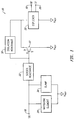
- FIG. 1 is a block diagram of preferred embodiment of the unbalanced mixer of the present invention.
- FIG. 2 is a schematic diagram of a preferred embodiment of the unbalanced mixer of this invention.
- FIG. 3 shows a schematic diagram of an alternate embodiment of an unbalanced mixer in accordance with the present invention.
- FIG. 4 depicts a specific implementation of the mixer of FIG. 3, in which the diodes comprising a clamp circuit are realized using diode-connected field-effect transistors.
- FIG. 1 is a block diagram of a preferred embodiment of the unbalanced mixer 10 of the present invention.
- the mixer 10 includes a transistor 12, which in an exemplary implementation is realized using a field-effect transistor (FET) having a control or gate (G) terminal, as well as drain (D) and source (S) terminals.
- FET field-effect transistor
- the mixer 10 includes a local oscillator (LO) input port 16, to which is applied an LO input signal, and further includes radio frequency (RF) and intermediate frequency (IF) signal ports 18 and 20.
- LO local oscillator
- RF radio frequency
- IF intermediate frequency
- input signals are applied to the LO and IF ports 20 and an output signal coupled from RF signal port 18.
- input signals are applied to the LO and RF ports 16 and 18, and output signal tapped from the IF signal port 20.
- the LO input port 16 receives the LO input signal over a 50 ⁇ transmission line (not shown), the reactance of a matching element 24 is selected to ensure that the impedance into LO port 16 is also 50 ⁇ .
- the LO input signal is coupled to the FET 12 through a series reactance 28.
- the input LO signal is amplified by a series resonator comprised of: (i) an inductive element within the series reactance 28, and (ii) the intrinsic gate-source capacitance (C gs ) of the FET 12.
- the series resonator becomes resonant at the frequency of the LO input signal, and hence reduces the required magnitude of the LO input signal.
- a clamp circuit 30 prevents negative half-cycles of the amplified LO input signal from causing reverse-breakdown at the transistor gate (G) by clamping the gate voltage to approximately one diode drop below the reference potential V REF .
- the mixer 10 further includes an isolation reactance 32 connected between the gate (G) and drain (D) of the transistor 12.
- an inductive component of the isolation reactance 32 and the intrinsic gate-drain capacitance (C gd ) of the transistor 12 form an "isolation resonator", which effectively decouples the transistor gate (G) from the drain (D) at the RF signal frequency.
- the isolation resonator approximates an open circuit at the frequency of the signal energy impressed upon the RF output port 18 by the drain (D) through diplexer 22.
- a capacitive component within the isolation reactance 32 provides the requisite low-frequency isolation between the IF signal port 20 and the transistor gate (G).
- the isolation reactance 32 enables the LO port 16 to be isolated from the RF port 18 without utilization of a balun, thereby enabling efficient realization of the mixer 10 as an integrated circuit.
- the isolation resonator also allows the achievement of a favorable third-order intercept point, since the reverse isolation effected thereby prevents RF and IF signal energy from being coupled to the gate (G) and influencing the conductance of the FET 12.
- the diplexer 22 includes capacitors C4 and C5, and an inductor L3.
- the inductor L3 serves to prevent higher frequency RF signal energy from being coupled from the transistor drain (D) to the IF signal 20.
- the isolation reactance 32 is seen to be comprised of an inductor L1 in series with a capacitor C3.
- L1 The value of L1 is selected such that the isolation resonator becomes resonant at the frequency of the RF signal energy coupled to the RF port 18 from the drain (D) of FET 12.
- Capacitor C3 provides isolation between the relatively low-frequency signals appearing at IF port 20 and the gate (G) of FET 12.
- the series reactance 28 at the gate (G) of FET 12 is seen to be comprised of an inductor L2 in series with a capacitor C2
- the inductor L2 in series with the intrinsic capacitance C gs of FET 12, forms a series resonator designed to amplify the LO input signal applied at the LO input port 16. This advantageously reduces the magnitude of LO input signal necessary to achieve a given level of RF output power when the mixer is configured as a frequency upconverter.
- the series resonator enhances efficiency by reducing the LO power level required to achieve a desired IF output power.
- the channel of transistor 12 is controlled only by the amplified LO input signal being applied to the transistor gate (G).
- the lack of DC bias is permitted by capacitor C2, which functions to allow the transistor 12 to achieve self-bias.
- Capacitor C1 is a DC blocking capacitor, which prevents DC offsets at the LO input port 16 from reaching the transistor gate (G). In addition, the capacitor C1 allows the clamping circuit 30 to attain self-bias.
- clamp circuit 30 is comprised of a diode-connected FET 104.
- FET 104 appears as a reverse-biased diode during positive half-cycles of the LO signal applied to LO port 16.
- the diode-connected transistor 104 becomes forward biased and hence clamps the applied LO input signal level.
- the matching element 24 should exhibit an inductive reactance in order that the impedance into the LO port 16 be approximately 50 ⁇ . Accordingly, in the implementation of FIG. 2 the matching element 24 comprises an inductor L4.
- FIG. 3 shows a schematic diagram of an alternate embodiment of an unbalanced mixer in accordance with the present invention.
- the mixers of FIGS. 2 and 3 are substantially similar, with the exception that the clamp circuit within the mixer of FIG. 3 is realized using parallel chains of series-connected diodes.
- the clamp circuit of FIG. 3 includes a first set of series-connected diodes D1-D3, connected in parallel with a second set of series-connected diodes D4-D6.
- FIG. 4 depicts a specific implementation of the mixer of FIG. 3, in which the diodes D1-D6 are realized using diode-connected field-effect transistors T1-T6.
Abstract
Description
- This invention relates generally to radio frequency mixers, and more particularly to mixers requiring reduced local oscillator drive levels and having high third order intercepts.
- The dynamic range of many prior art microwave front-ends is controlled by the single and two-tone intermodulation levels of the mixers therein. Typical high-performance mixers obtain third order intercept points approximately equal to the local oscillator (LO) power minus the conversion loss plus 10-dB. Trade-offs between LO power levels and third order intercept and one dB compression points are inevitable, even in complex multiple device schemes attempting to improve isolation, bandwidth, and single-tone intermodulation levels.
- When the channel of a field-effect transistor (FET) comprises the mixing element, low-distortion mixing has been shown to be possible even at moderate LO power levels. (See, Stephen A. Maas, "A GaAs MESFET Balanced Mixer With Very Low Intermodulation," 1987 IEEE MTT-S Digest, pp,895-896.). Recently, both "single-balanced" and "double-balanced" FET mixers have been designed for operation over relatively wide frequency ranges (e.g., 2-8 GHz). The characterization of a mixer as "single-balanced" indicates that a balun is coupled to one of the mixer ports (e.g., the LO port), while a "double-balanced" mixer includes baluns at two of the three ports. Baluns advantageously improve isolation between mixer ports, but are often realized as bulky, coiled-wire discrete components. When implemented as integrated circuits, baluns tend to require a large wafer area, thus undesirably increasing cost and circuit dimensions.
- The dynamic range of existing FET mixers is a function both of the DC operating characteristics of the FET devices included therein, as well as of the LO drive level. Conventional DC bias techniques, including those involving the application of externally-supplied DC gate voltages, have required substantial LO drive levels in applications requiring significant dynamic range. This has generally required the inclusion of relatively high-power RF amplifiers in the "pumping" circuits used to generate the LO drive signals, often resulting in increased circuit cost and complexity. Hence, there is an interest in reducing the LO drive levels required to be supplied to FET mixers.
- Briefly, the mixer includes an input or local oscillator (LO) port for receiving an input signal. A first transistor has a control terminal coupled to the mixer input port, and an output terminal coupled to a first signal port of the mixer. The mixer further includes a resonator circuit, connected between the transistor control and signal terminals, for providing signal isolation between the mixer LO port and the signal port. In a preferred embodiment the resonator circuit comprises an inductive element in parallel with a first intrinsic capacitance of the transistor.
- The mixer may also include a diplexer circuit for coupling signal energy of a first frequency between the output terminal to the first signal port, and for coupling signal energy of a second frequency between the output terminal and a second signal port. A series resonant circuit, connected between the input or LO port and the transistor control terminal, may also be provided for amplifying the input signal. In a preferred embodiment the series resonant circuit comprises an input inductive element and an input intrinsic capacitance of the first transistor.
- One advantage provided by an embodiment of this invention is that isolation of the LO port from the other mixer signal ports is achieved without use of a balun. A radio frequency mixer provided in accordance with an embodiment of the present invention is not reliant upon a balun to achieve a high third-order intercept.
- Another advantage provided by an embodiment of the present invention is that the mixer is capable of operation in the absence of DC bias.
- Yet another advantage provided by an embodiment of this invention is that the resonator circuit improves the third order intercept point by preventing signal energy from being coupled from the mixer signal ports connected to the transistor output port to the transistor control terminal.
- A further advantage provided by an embodiment of this invention is that operation over a wide dynamic range at reduced LO drive levels is exhibited.
- These and other objects and advantages of this invention will no doubt become obvious to those of ordinary skill in the art after having read the following detailed description of the preferred embodiments which are illustrated in the various drawing figures.
- FIG. 1 is a block diagram of preferred embodiment of the unbalanced mixer of the present invention.
- FIG. 2 is a schematic diagram of a preferred embodiment of the unbalanced mixer of this invention.
- FIG. 3 shows a schematic diagram of an alternate embodiment of an unbalanced mixer in accordance with the present invention.
- FIG. 4 depicts a specific implementation of the mixer of FIG. 3, in which the diodes comprising a clamp circuit are realized using diode-connected field-effect transistors.
- FIG. 1 is a block diagram of a preferred embodiment of the
unbalanced mixer 10 of the present invention. Themixer 10 includes atransistor 12, which in an exemplary implementation is realized using a field-effect transistor (FET) having a control or gate (G) terminal, as well as drain (D) and source (S) terminals. Themixer 10 includes a local oscillator (LO)input port 16, to which is applied an LO input signal, and further includes radio frequency (RF) and intermediate frequency (IF)signal ports diplexer 22, interposed between the drain (D) and thesignal ports mixer 10 is operational as a frequency upconverter, input signals are applied to the LO andIF ports 20 and an output signal coupled fromRF signal port 18. During operation as a frequency downconverter, input signals are applied to the LO andRF ports IF signal port 20. - Since in a exemplary implementation the
LO input port 16 receives the LO input signal over a 50Ω transmission line (not shown), the reactance of amatching element 24 is selected to ensure that the impedance intoLO port 16 is also 50Ω. As is indicated by FIG. 1, the LO input signal is coupled to theFET 12 through aseries reactance 28. In accordance with one aspect of the invention, the input LO signal is amplified by a series resonator comprised of: (i) an inductive element within theseries reactance 28, and (ii) the intrinsic gate-source capacitance (Cgs) of theFET 12. The series resonator becomes resonant at the frequency of the LO input signal, and hence reduces the required magnitude of the LO input signal. Aclamp circuit 30 prevents negative half-cycles of the amplified LO input signal from causing reverse-breakdown at the transistor gate (G) by clamping the gate voltage to approximately one diode drop below the reference potential VREF. - The
mixer 10 further includes anisolation reactance 32 connected between the gate (G) and drain (D) of thetransistor 12. In accordance with one aspect of the present invention, an inductive component of theisolation reactance 32 and the intrinsic gate-drain capacitance (Cgd) of thetransistor 12 form an "isolation resonator", which effectively decouples the transistor gate (G) from the drain (D) at the RF signal frequency. In particular, the isolation resonator approximates an open circuit at the frequency of the signal energy impressed upon theRF output port 18 by the drain (D) throughdiplexer 22. In addition, a capacitive component within theisolation reactance 32 provides the requisite low-frequency isolation between theIF signal port 20 and the transistor gate (G). In this way theisolation reactance 32 enables theLO port 16 to be isolated from theRF port 18 without utilization of a balun, thereby enabling efficient realization of themixer 10 as an integrated circuit. The isolation resonator also allows the achievement of a favorable third-order intercept point, since the reverse isolation effected thereby prevents RF and IF signal energy from being coupled to the gate (G) and influencing the conductance of theFET 12. - Referring now to FIG. 2, there is shown a schematic diagram of a preferred embodiment of an
unbalanced mixer 100 of the present invention. As is indicated by FIG. 2, thediplexer 22 includes capacitors C4 and C5, and an inductor L3. The inductor L3 serves to prevent higher frequency RF signal energy from being coupled from the transistor drain (D) to theIF signal 20. In the embodiment of FIG. 2, theisolation reactance 32 is seen to be comprised of an inductor L1 in series with a capacitor C3. The inductor L1, in parallel with the intrinsic capacitance Cgd ofFET 12, together form an isolation resonator. The value of L1 is selected such that the isolation resonator becomes resonant at the frequency of the RF signal energy coupled to theRF port 18 from the drain (D) ofFET 12. Capacitor C3 provides isolation between the relatively low-frequency signals appearing atIF port 20 and the gate (G) ofFET 12. - The
series reactance 28 at the gate (G) ofFET 12 is seen to be comprised of an inductor L2 in series with a capacitor C2 The inductor L2, in series with the intrinsic capacitance Cgs ofFET 12, forms a series resonator designed to amplify the LO input signal applied at theLO input port 16. This advantageously reduces the magnitude of LO input signal necessary to achieve a given level of RF output power when the mixer is configured as a frequency upconverter. When the mixer is configured as a frequency downconverter, the series resonator enhances efficiency by reducing the LO power level required to achieve a desired IF output power. Since a DC bias current is not supplied to thetransistor 12, the channel oftransistor 12 is controlled only by the amplified LO input signal being applied to the transistor gate (G). The lack of DC bias is permitted by capacitor C2, which functions to allow thetransistor 12 to achieve self-bias. - Capacitor C1 is a DC blocking capacitor, which prevents DC offsets at the
LO input port 16 from reaching the transistor gate (G). In addition, the capacitor C1 allows the clampingcircuit 30 to attain self-bias. - As mentioned above, reverse breakdown at the gate of
FET 12 is prevented byclamp circuit 30. In the embodiment of FIG. 2,clamp circuit 30 is comprised of a diode-connectedFET 104. In operation,FET 104 appears as a reverse-biased diode during positive half-cycles of the LO signal applied toLO port 16. When the magnitude of negative half-cycles of the LO signal exceed approximately one diode drop (e.g., 0.7V), the diode-connectedtransistor 104 becomes forward biased and hence clamps the applied LO input signal level. In an exemplary embodiment it has been found that the matchingelement 24 should exhibit an inductive reactance in order that the impedance into theLO port 16 be approximately 50Ω. Accordingly, in the implementation of FIG. 2 thematching element 24 comprises an inductor L4. - FIG. 3 shows a schematic diagram of an alternate embodiment of an unbalanced mixer in accordance with the present invention. The mixers of FIGS. 2 and 3 are substantially similar, with the exception that the clamp circuit within the mixer of FIG. 3 is realized using parallel chains of series-connected diodes. In particular, the clamp circuit of FIG. 3 includes a first set of series-connected diodes D1-D3, connected in parallel with a second set of series-connected diodes D4-D6. FIG. 4 depicts a specific implementation of the mixer of FIG. 3, in which the diodes D1-D6 are realized using diode-connected field-effect transistors T1-T6.
- Although this invention has been described in terms of the presently preferred embodiments, it is to be understood that the disclosure is not to be interpreted as limiting. Various alterations and modifications will no doubt become apparent to those skilled in the art after having read the above disclosure. Accordingly, it is intended that the appended claims be interpreted as covering all alterations and modifications as fall within the true spirit and scope of the invention.
Claims (13)
- A mixer, comprising:an input port for receiving an input signal;a first transistor having a control terminal coupled to said input port, and an output terminal coupled to a first signal port, anda resonator connected between said control terminal and said output terminal, said resonator circuit providing signal isolation between said input port and said first signal port.
- The mixer of claim 1 further including a diplexer circuit for coupling signal energy of a first frequency between said output terminal and first signal port, and for coupling signal energy of a second frequency between said output terminal and a second signal port.
- The mixer of claim 1 or 2 wherein said resonator circuit comprises an inductive element in parallel with a first intrinsic capacitance of said transistor.
- The mixer of any one of claims 1 to 3 further including a series resonant circuit connected to said input terminal, said series resonant circuit including an input inductive element and an input intrinsic capacitance of said first transistor.
- The mixer of any one of claims 1 to 4 further including a reverse-breakdown prevention circuit, connected to said input port of said mixer, for preventing said input signal from causing reverse-breakdown at said input terminal of said first transistor.
- The mixer of claim 4 further including a reverse-breakdown prevention circuit, connected in parallel with said series resonant circuit at said input port of said mixer, for preventing said input signal from causing reverse-breakdown at said input terminal of said first transistor.
- An unbalanced FET mixer, comprising:a first FET transistor having a gate, a drain ad a source, said gate being coupled to a first port of said mixer;a diplexer circuit interposed between said drain and second and third ports of said mixer; anda resonator circuit connected between said gate and drain, said resonator circuit providing signal isolation between said first and second ports of said mixer.
- The mixer of claim 7 wherein said diplexer circuit includes inductive and capacitive circuit elements for coupling signal energy of a first frequency between said drain and said second port, and for coupling signal energy of a second frequency between said drain and said third port.
- The mixer of claims 7 or 8 wherein said resonator circuit comprises an inductive element in parallel with a gate-drain capacitance of said FET transistor.
- The mixer of any one of claims 7 to 9 further including a series resonant circuit at said gate of said first FET transistor, said series resonant circuit including an input inductive element and a gate-source capacitance of said first FET transistor.
- The mixer of any one of claims 7 to 10 further including a reverse-breakdown prevention circuit, connected to an input port of said mixer, for preventing an input signal applied to said input port from causing reverse-breakdown at said gate of said first FET transistor.
- An unbalanced FET mixer, comprising:a local oscillator (LO) port for receiving a local oscillator signal;a first FET transistor having a gate, a drain and a source, said gate being coupled to said LO port;a diplexer circuit interposed between said drain and radio frequency (RF) and intermediate frequency (IF) ports of said mixer; anda resonator circuit connected between said gate and drain, said resonator circuit providing signal isolation between said RF and LO ports of said mixer.
- The mixer of claim 12 further including a series resonant circuit connected between said LO port and said gate of said FET transistor, said series resonant circuit being resonant at a frequency of said local oscillator signal.
Priority Applications (2)
| Application Number | Priority Date | Filing Date | Title |
|---|---|---|---|
| EP19960302777 EP0802625B1 (en) | 1996-04-19 | 1996-04-19 | Unbalanced fet mixer |
| DE69628816T DE69628816D1 (en) | 1996-04-19 | 1996-04-19 | FET mixer that is not implemented in a push-pull circuit |
Applications Claiming Priority (1)
| Application Number | Priority Date | Filing Date | Title |
|---|---|---|---|
| EP19960302777 EP0802625B1 (en) | 1996-04-19 | 1996-04-19 | Unbalanced fet mixer |
Publications (2)
| Publication Number | Publication Date |
|---|---|
| EP0802625A1 true EP0802625A1 (en) | 1997-10-22 |
| EP0802625B1 EP0802625B1 (en) | 2003-06-25 |
Family
ID=8224895
Family Applications (1)
| Application Number | Title | Priority Date | Filing Date |
|---|---|---|---|
| EP19960302777 Expired - Lifetime EP0802625B1 (en) | 1996-04-19 | 1996-04-19 | Unbalanced fet mixer |
Country Status (2)
| Country | Link |
|---|---|
| EP (1) | EP0802625B1 (en) |
| DE (1) | DE69628816D1 (en) |
Cited By (1)
| Publication number | Priority date | Publication date | Assignee | Title |
|---|---|---|---|---|
| ES2177402A1 (en) * | 2000-07-03 | 2002-12-01 | Univ Malaga | Frequency mixer circuit for microwave / precise transceiver |
Citations (4)
| Publication number | Priority date | Publication date | Assignee | Title |
|---|---|---|---|---|
| DE2816586A1 (en) * | 1977-04-18 | 1978-11-23 | Hitachi Ltd | SELF-VIBRATING MIXING CIRCUIT |
| US4949398A (en) * | 1988-06-09 | 1990-08-14 | The Aerospace Corporation | GaAs MESFET balanced resistive mixer |
| US5060298A (en) * | 1988-12-09 | 1991-10-22 | Siemens Aktiengesellschaft | Monolithic double balanced mixer with high third order intercept point employing an active distributed balun |
| US5263198A (en) * | 1991-11-05 | 1993-11-16 | Honeywell Inc. | Resonant loop resistive FET mixer |
-
1996
- 1996-04-19 EP EP19960302777 patent/EP0802625B1/en not_active Expired - Lifetime
- 1996-04-19 DE DE69628816T patent/DE69628816D1/en not_active Expired - Lifetime
Patent Citations (4)
| Publication number | Priority date | Publication date | Assignee | Title |
|---|---|---|---|---|
| DE2816586A1 (en) * | 1977-04-18 | 1978-11-23 | Hitachi Ltd | SELF-VIBRATING MIXING CIRCUIT |
| US4949398A (en) * | 1988-06-09 | 1990-08-14 | The Aerospace Corporation | GaAs MESFET balanced resistive mixer |
| US5060298A (en) * | 1988-12-09 | 1991-10-22 | Siemens Aktiengesellschaft | Monolithic double balanced mixer with high third order intercept point employing an active distributed balun |
| US5263198A (en) * | 1991-11-05 | 1993-11-16 | Honeywell Inc. | Resonant loop resistive FET mixer |
Non-Patent Citations (2)
| Title |
|---|
| CHANG K W ET AL: "ZERO BIAS GAINAS MISFET MIXERS", INTERNATIONAL MICROWAVE SYMPOSIUM, LONG BEACH, JUNE 13 - 15, 1989. VOLUMES 1 - 3 BOUND AS ONE, vol. 1, 13 June 1989 (1989-06-13), INSTITUTE OF ELECTRICAL AND ELECTRONICS ENGINEERS, pages 1027 - 1030, XP000077291 * |
| S. A. MAAS: "A GaAs MESFET Mixer with Very Low Intermodulation", IEEE TRANSACTIONS ON MICROWAVE THEORY AND TECHNIQUES, vol. 35, no. 4, April 1987 (1987-04-01), NEW YORK US, pages 425 - 429, XP002006781 * |
Cited By (1)
| Publication number | Priority date | Publication date | Assignee | Title |
|---|---|---|---|---|
| ES2177402A1 (en) * | 2000-07-03 | 2002-12-01 | Univ Malaga | Frequency mixer circuit for microwave / precise transceiver |
Also Published As
| Publication number | Publication date |
|---|---|
| EP0802625B1 (en) | 2003-06-25 |
| DE69628816D1 (en) | 2003-07-31 |
Similar Documents
| Publication | Publication Date | Title |
|---|---|---|
| US5678226A (en) | Unbalanced FET mixer | |
| US5752181A (en) | Method and apparatus for reducing inermodulation distortion in a mixer | |
| CA2524751C (en) | Passive reflection mixer | |
| US6892062B2 (en) | Current-reuse bleeding mixer | |
| US6057714A (en) | Double balance differential active ring mixer with current shared active input balun | |
| US6871059B1 (en) | Passive balun FET mixer | |
| US5027163A (en) | High level wide band RF mixer | |
| US6798268B2 (en) | Single-ended differential circuit using complementary devices | |
| US5799248A (en) | Quasi-double balanced passive reflection FET mixer | |
| US4949398A (en) | GaAs MESFET balanced resistive mixer | |
| US5513390A (en) | Biased FET mixer | |
| US5732345A (en) | Quasi-double balanced dual-transformer dual FET mixer, which achieves better isolation by using a first and second diplexer, and a transmission line RF balun | |
| US4677691A (en) | Microwave receiver | |
| US5789963A (en) | Low power consumption mixer and frequency conversion with inter-terminal isolation for stable mixing | |
| KR19990008262A (en) | Compensation ring mixer | |
| JP3339892B2 (en) | Integrated circuit and method of using same | |
| US6861891B2 (en) | Sub-harmonic mixer | |
| EP0802625B1 (en) | Unbalanced fet mixer | |
| CA2174395C (en) | Unbalanced fet mixer | |
| KR100407841B1 (en) | Unbalanced Field Effect Transistor Mixer | |
| KR100262455B1 (en) | Negative self-bias circuit for fet mixers | |
| JPH09284057A (en) | Unbalanced fet mixer | |
| JP2004215314A (en) | Unbalanced fet mixer | |
| KR890004205B1 (en) | Television tuner for wideband receive | |
| KR0135020B1 (en) | Uhf-band mmic source mixer for front end receiver |
Legal Events
| Date | Code | Title | Description |
|---|---|---|---|
| PUAI | Public reference made under article 153(3) epc to a published international application that has entered the european phase |
Free format text: ORIGINAL CODE: 0009012 |
|
| AK | Designated contracting states |
Kind code of ref document: A1 Designated state(s): DE FI FR GB IT SE |
|
| 17P | Request for examination filed |
Effective date: 19980421 |
|
| 17Q | First examination report despatched |
Effective date: 20001206 |
|
| GRAG | Despatch of communication of intention to grant |
Free format text: ORIGINAL CODE: EPIDOS AGRA |
|
| GRAG | Despatch of communication of intention to grant |
Free format text: ORIGINAL CODE: EPIDOS AGRA |
|
| GRAG | Despatch of communication of intention to grant |
Free format text: ORIGINAL CODE: EPIDOS AGRA |
|
| GRAH | Despatch of communication of intention to grant a patent |
Free format text: ORIGINAL CODE: EPIDOS IGRA |
|
| GRAH | Despatch of communication of intention to grant a patent |
Free format text: ORIGINAL CODE: EPIDOS IGRA |
|
| GRAA | (expected) grant |
Free format text: ORIGINAL CODE: 0009210 |
|
| AK | Designated contracting states |
Designated state(s): DE FI FR GB IT SE |
|
| PG25 | Lapsed in a contracting state [announced via postgrant information from national office to epo] |
Ref country code: IT Free format text: LAPSE BECAUSE OF FAILURE TO SUBMIT A TRANSLATION OF THE DESCRIPTION OR TO PAY THE FEE WITHIN THE PRESCRIBED TIME-LIMIT;WARNING: LAPSES OF ITALIAN PATENTS WITH EFFECTIVE DATE BEFORE 2007 MAY HAVE OCCURRED AT ANY TIME BEFORE 2007. THE CORRECT EFFECTIVE DATE MAY BE DIFFERENT FROM THE ONE RECORDED. Effective date: 20030625 Ref country code: FR Free format text: LAPSE BECAUSE OF FAILURE TO SUBMIT A TRANSLATION OF THE DESCRIPTION OR TO PAY THE FEE WITHIN THE PRESCRIBED TIME-LIMIT Effective date: 20030625 |
|
| REG | Reference to a national code |
Ref country code: GB Ref legal event code: FG4D |
|
| REF | Corresponds to: |
Ref document number: 69628816 Country of ref document: DE Date of ref document: 20030731 Kind code of ref document: P |
|
| PG25 | Lapsed in a contracting state [announced via postgrant information from national office to epo] |
Ref country code: SE Free format text: LAPSE BECAUSE OF FAILURE TO SUBMIT A TRANSLATION OF THE DESCRIPTION OR TO PAY THE FEE WITHIN THE PRESCRIBED TIME-LIMIT Effective date: 20030925 |
|
| PG25 | Lapsed in a contracting state [announced via postgrant information from national office to epo] |
Ref country code: DE Free format text: LAPSE BECAUSE OF FAILURE TO SUBMIT A TRANSLATION OF THE DESCRIPTION OR TO PAY THE FEE WITHIN THE PRESCRIBED TIME-LIMIT Effective date: 20030926 |
|
| PGFP | Annual fee paid to national office [announced via postgrant information from national office to epo] |
Ref country code: FR Payment date: 20040420 Year of fee payment: 9 |
|
| PLBE | No opposition filed within time limit |
Free format text: ORIGINAL CODE: 0009261 |
|
| STAA | Information on the status of an ep patent application or granted ep patent |
Free format text: STATUS: NO OPPOSITION FILED WITHIN TIME LIMIT |
|
| 26N | No opposition filed |
Effective date: 20040326 |
|
| EN | Fr: translation not filed | ||
| PGFP | Annual fee paid to national office [announced via postgrant information from national office to epo] |
Ref country code: GB Payment date: 20060424 Year of fee payment: 11 |
|
| PGFP | Annual fee paid to national office [announced via postgrant information from national office to epo] |
Ref country code: FI Payment date: 20060427 Year of fee payment: 11 |
|
| GBPC | Gb: european patent ceased through non-payment of renewal fee |
Effective date: 20070419 |
|
| PG25 | Lapsed in a contracting state [announced via postgrant information from national office to epo] |
Ref country code: FI Free format text: LAPSE BECAUSE OF NON-PAYMENT OF DUE FEES Effective date: 20070419 |
|
| PG25 | Lapsed in a contracting state [announced via postgrant information from national office to epo] |
Ref country code: GB Free format text: LAPSE BECAUSE OF NON-PAYMENT OF DUE FEES Effective date: 20070419 |