EP0803867A2 - Optical head device - Google Patents
Optical head device Download PDFInfo
- Publication number
- EP0803867A2 EP0803867A2 EP97101875A EP97101875A EP0803867A2 EP 0803867 A2 EP0803867 A2 EP 0803867A2 EP 97101875 A EP97101875 A EP 97101875A EP 97101875 A EP97101875 A EP 97101875A EP 0803867 A2 EP0803867 A2 EP 0803867A2
- Authority
- EP
- European Patent Office
- Prior art keywords
- light
- wavelength
- optical
- reflected
- allows
- Prior art date
- Legal status (The legal status is an assumption and is not a legal conclusion. Google has not performed a legal analysis and makes no representation as to the accuracy of the status listed.)
- Granted
Links
Images


Classifications
-
- G—PHYSICS
- G11—INFORMATION STORAGE
- G11B—INFORMATION STORAGE BASED ON RELATIVE MOVEMENT BETWEEN RECORD CARRIER AND TRANSDUCER
- G11B7/00—Recording or reproducing by optical means, e.g. recording using a thermal beam of optical radiation by modifying optical properties or the physical structure, reproducing using an optical beam at lower power by sensing optical properties; Record carriers therefor
- G11B7/12—Heads, e.g. forming of the optical beam spot or modulation of the optical beam
- G11B7/135—Means for guiding the beam from the source to the record carrier or from the record carrier to the detector
- G11B7/1353—Diffractive elements, e.g. holograms or gratings
-
- G—PHYSICS
- G11—INFORMATION STORAGE
- G11B—INFORMATION STORAGE BASED ON RELATIVE MOVEMENT BETWEEN RECORD CARRIER AND TRANSDUCER
- G11B7/00—Recording or reproducing by optical means, e.g. recording using a thermal beam of optical radiation by modifying optical properties or the physical structure, reproducing using an optical beam at lower power by sensing optical properties; Record carriers therefor
- G11B7/12—Heads, e.g. forming of the optical beam spot or modulation of the optical beam
- G11B7/123—Integrated head arrangements, e.g. with source and detectors mounted on the same substrate
-
- G—PHYSICS
- G11—INFORMATION STORAGE
- G11B—INFORMATION STORAGE BASED ON RELATIVE MOVEMENT BETWEEN RECORD CARRIER AND TRANSDUCER
- G11B7/00—Recording or reproducing by optical means, e.g. recording using a thermal beam of optical radiation by modifying optical properties or the physical structure, reproducing using an optical beam at lower power by sensing optical properties; Record carriers therefor
- G11B7/12—Heads, e.g. forming of the optical beam spot or modulation of the optical beam
- G11B7/125—Optical beam sources therefor, e.g. laser control circuitry specially adapted for optical storage devices; Modulators, e.g. means for controlling the size or intensity of optical spots or optical traces
- G11B7/127—Lasers; Multiple laser arrays
- G11B7/1275—Two or more lasers having different wavelengths
-
- G—PHYSICS
- G11—INFORMATION STORAGE
- G11B—INFORMATION STORAGE BASED ON RELATIVE MOVEMENT BETWEEN RECORD CARRIER AND TRANSDUCER
- G11B7/00—Recording or reproducing by optical means, e.g. recording using a thermal beam of optical radiation by modifying optical properties or the physical structure, reproducing using an optical beam at lower power by sensing optical properties; Record carriers therefor
- G11B7/12—Heads, e.g. forming of the optical beam spot or modulation of the optical beam
- G11B7/13—Optical detectors therefor
- G11B7/131—Arrangement of detectors in a multiple array
-
- G—PHYSICS
- G11—INFORMATION STORAGE
- G11B—INFORMATION STORAGE BASED ON RELATIVE MOVEMENT BETWEEN RECORD CARRIER AND TRANSDUCER
- G11B7/00—Recording or reproducing by optical means, e.g. recording using a thermal beam of optical radiation by modifying optical properties or the physical structure, reproducing using an optical beam at lower power by sensing optical properties; Record carriers therefor
- G11B7/12—Heads, e.g. forming of the optical beam spot or modulation of the optical beam
- G11B7/135—Means for guiding the beam from the source to the record carrier or from the record carrier to the detector
- G11B7/1356—Double or multiple prisms, i.e. having two or more prisms in cooperation
-
- G—PHYSICS
- G11—INFORMATION STORAGE
- G11B—INFORMATION STORAGE BASED ON RELATIVE MOVEMENT BETWEEN RECORD CARRIER AND TRANSDUCER
- G11B7/00—Recording or reproducing by optical means, e.g. recording using a thermal beam of optical radiation by modifying optical properties or the physical structure, reproducing using an optical beam at lower power by sensing optical properties; Record carriers therefor
- G11B7/12—Heads, e.g. forming of the optical beam spot or modulation of the optical beam
- G11B7/135—Means for guiding the beam from the source to the record carrier or from the record carrier to the detector
- G11B7/1365—Separate or integrated refractive elements, e.g. wave plates
- G11B7/1367—Stepped phase plates
-
- G—PHYSICS
- G11—INFORMATION STORAGE
- G11B—INFORMATION STORAGE BASED ON RELATIVE MOVEMENT BETWEEN RECORD CARRIER AND TRANSDUCER
- G11B7/00—Recording or reproducing by optical means, e.g. recording using a thermal beam of optical radiation by modifying optical properties or the physical structure, reproducing using an optical beam at lower power by sensing optical properties; Record carriers therefor
- G11B7/12—Heads, e.g. forming of the optical beam spot or modulation of the optical beam
- G11B7/135—Means for guiding the beam from the source to the record carrier or from the record carrier to the detector
- G11B7/1381—Non-lens elements for altering the properties of the beam, e.g. knife edges, slits, filters or stops
-
- G—PHYSICS
- G11—INFORMATION STORAGE
- G11B—INFORMATION STORAGE BASED ON RELATIVE MOVEMENT BETWEEN RECORD CARRIER AND TRANSDUCER
- G11B7/00—Recording or reproducing by optical means, e.g. recording using a thermal beam of optical radiation by modifying optical properties or the physical structure, reproducing using an optical beam at lower power by sensing optical properties; Record carriers therefor
- G11B7/12—Heads, e.g. forming of the optical beam spot or modulation of the optical beam
- G11B7/135—Means for guiding the beam from the source to the record carrier or from the record carrier to the detector
- G11B7/139—Numerical aperture control means
-
- G—PHYSICS
- G11—INFORMATION STORAGE
- G11B—INFORMATION STORAGE BASED ON RELATIVE MOVEMENT BETWEEN RECORD CARRIER AND TRANSDUCER
- G11B7/00—Recording or reproducing by optical means, e.g. recording using a thermal beam of optical radiation by modifying optical properties or the physical structure, reproducing using an optical beam at lower power by sensing optical properties; Record carriers therefor
- G11B7/12—Heads, e.g. forming of the optical beam spot or modulation of the optical beam
- G11B7/135—Means for guiding the beam from the source to the record carrier or from the record carrier to the detector
- G11B7/1395—Beam splitters or combiners
-
- G—PHYSICS
- G11—INFORMATION STORAGE
- G11B—INFORMATION STORAGE BASED ON RELATIVE MOVEMENT BETWEEN RECORD CARRIER AND TRANSDUCER
- G11B7/00—Recording or reproducing by optical means, e.g. recording using a thermal beam of optical radiation by modifying optical properties or the physical structure, reproducing using an optical beam at lower power by sensing optical properties; Record carriers therefor
- G11B2007/0003—Recording, reproducing or erasing systems characterised by the structure or type of the carrier
- G11B2007/0006—Recording, reproducing or erasing systems characterised by the structure or type of the carrier adapted for scanning different types of carrier, e.g. CD & DVD
Definitions
- Thin invention relates to an optical head device used for the recording or reproducing of an optical recording medium, and more particularly to, an optical head device used for the recording or reproducing of two kinds of optical recording mediums with different substrate thicknesses.
- an optical disk with large storage capacity such as a digital video disk
- an optical disk with a substrate thickness of 0.6 mm is used.
- an optical disk with a substrate thickness of 1.2 mm is used.
- an optical head device which can be used for the reproducing of both the digital video disk and compact disk.
- FIG.1 shows a composition of a conventional optical head device.
- a composition of a conventional optical head device As shown in FIG.1, around half of emitted light from a semiconductor laser 237 is reflected by a half mirror 238, being transmitted through an aperture 239, entering an optical path control device 240, thereby being divided into a first light and a second light.
- the first light emitted from the optical path control device 240 is transmitted through a collimator lens 4, entering an objective lens 6 as a collimated light, thereby being focused on a disk 7 which is a first optical disk such as a digital video disk with a substrate thickness of 0.6 mm.
- the second light emitted from the optical path control device 240 is transmitted through the collimator lens 4, entering the objective lens 6 as a divergent light, thereby being focused on a disk 8 which is a second optical disk such as a compact disk with a substrate thickness of 1.2 mm.
- the first and second lights are reflected on the disk 7 and disk 8, respectively, being reversely transmitted through the objective lens 6, collimator lens 4, optical path control device 240 and aperture 239, around its half being transmitted through the half mirror 238, further being transmitted through a concave lens 241, being received by an optical detector 242.
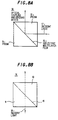
- FIGS.2A and 2B show a composition of the optical path control device 240.
- the optical path control device 240 is composed of a prism 243 and a prism 244 which are adhered through a polarization separating film 245.
- the polarization separating film 245 has a function that a P-polarization component of an incident light is all transmitted through and a S-polarization component of the incident light is all reflected on.
- an incident light 249, which is a S-polarization component to the polarization separating film 245, as shown in FIG.2B, is all reflected on the polarization separating film 245, being emitted from the prism 243 as the second light.
- the optical path control device 240 effective optical path lengths as to the first and second lights are differed from each other, i.e., the effective optical path length from the semiconductor laser 237 to the collimator lens 4 as to the second light is shorter than that as to the first light.
- the effective optical path length from the semiconductor laser 237 to the collimator lens 4 is adjusted such that the first light enters the objective lens 6 as a collimated light, the second light will enter the objective lens 6 as a divergent light.
- the objective lens 6 has a spherical aberration that cancels a spherical aberration occurred when a collimated light entering the objective lens 6 is transmitted through a substrate with a thickness of 0.6 mm. Therefore, when the collimated light entering the objective lens 6 is transmitted through a substrate with a thickness of 1.2 mm, there remains a spherical aberration. However, if a divergent light enters the objective lens 6, there occurs a new spherical aberration due to a movement of image point of the objective lens 6, thereby the remaining spherical aberration when transmitting through the substrate with 1.2 mm thickness being canceled.
- the first light can be focused on the disk 7 with a substrate thickness of 0.6 mm with no aberration
- the second light can be focused on the disk 8 with a substrate thickness of 1.2 mm with no aberration.
- a numerical aperture of objective lens in the standard of compact disk is to be smaller than that in the standard of digital video disk.
- the effective optical path lengths as to the first and second lights are differed from each other, by providing the aperture 239 in the optical system, the beam diameter of the second light entering the objective lens 6 can be smaller than the beam diameter of the first light entering the objective lens 6. Therefore, the effective numerical aperture as to the second light of the objective lens 6 is smaller than the effective numerical aperture as to the first light of the objective lens 6, thereby the above requirement being satisfied.
- FIGS.3A and 3B show another composition of the optical path control device 240 in the optical head device in FIG.1.
- the optical path control device 240 is composed of a prism 10 and a hologram 250 which is formed on the oblique plane of the prism 10.
- an incident light 248, which is a P-polarization component to the hologram 250, as shown in FIG.3A is reflected and diffracted as a +1st-order diffraction light by the hologram 250, then being emitted from the prism 10 as the second light.
- an incident light 249 which is a S-polarization component to the hologram 250, an shown in FIG.3B, is all reflected by the hologram 250, being emitted from the prism 10 as the first light.
- FIG.4 shows a composition of the hologram 250 in FIGS.3A and 3B.
- the hologram 250 is composed of a polarization separating film 251 and a hologram layer 252 which are formed on the oblige plane of the prism 10.
- the polarization separating film 251 has a function that a P-polarization component of an incident light is all transmitted through and a S-polarization component of the incident light is all reflected on.
- the hologram 250 functions as a convex surface mirror to a +1st-order diffraction light.
- the incident light 248, which is a P-polarization component to the polarization separating film 251 is all transmitted through the polarization separating film 251, being reflected and diffracted as a +1st-order diffraction light by the hologram layer 252, again being all transmitted through the polarization separating film 251, then being emitted from the hologram 250 as the second light.
- the incident light 249, which is a S-polarization component to the polarization separating film 251 is all reflected by the polarization separating film 251, being emitted from the hologram 250 as the first light.
- the incident light 248 which is a P-polarization component to the polarization separating film 251
- the optical path control device 240 As shown in FIGS.3A and 3B, an apparent luminous point to the second light becomes closer to the optical path control device 240 than that to the first light. Therefore, the effective optical path length from the semiconductor laser 237 to the collimator lens 4 as to the second light can be shorter than that as to the first light.
- the conventional optical head device as shown in FIG.1 has a first problem that, since the incident light is divided into the first and second lights by the optical path control device 240, the utilization efficiency as to the respective lights is reduced by half. Namely, if the semiconductor laser 237 has the same output power as that of an usual optical head device, the amount of light received by the optical detector 242 is reduced by half of that in the usual optical head device, thereby the signal-to-noise ratio(S/N ratio) of a reproduced signal being reduced. Thus, to make the amount of light received by the optical detector 242 equal to that in the usual optical head device, the output power of the semiconductor laser 237 needs to be two times that in the usual optical head device. If the recording of the disks 7, 8 is performed as well as the reproducing, the output power of the semiconductor laser 237 needs to be further increased, i.e., it is substantially impossible.
- the conventional optical head device as shown in FIG.1 has a second problem, which is related to a wavelength of light emitted from the semiconductor laser 237.
- a wavelength of 635 nm to 650 is used, and, in the standard of compact disk, a wavelength of 785 nm is used.
- a semiconductor laser which outputs light with a wavelength of 635 to 650 nm needs to be used since it can give a more reduced diameter of focused spot.
- compact disk there is a rewritable-type compact disk.
- the rewritable-type compact disk has a high reflection factor more than 70 % in 785 nm wavelength, it has a low reflection factor of around 10 % in a wavelength of 635 to 650 nm. Therefore, it is impossible for a conventional optical head device which is adapted to a wavelength of 635 to 650 nm to be used in the reproducing of the rewritable-type compact disk.
- an object of the invention to provide an optical head device which is used for the recording or reproducing of two kinds of optical recording mediums with different substrate thicknesses, in which a reproduced signal has a S/N ratio equal to that in an usual optical head device and a semiconductor laser is only required to have an output power equal to that in an usual optical head device.
- an optical head device comprises:
- an optical head device comprises:
- an optical head device comprises:
- an optical head device comprises:
- FIG.5 An optical head device in the first preferred embodiment will be explained in FIG.5, wherein like parts are indicated by like reference numerals as used in FIG.1.
- both a module 1 and a module 2 include a semiconductor laser and an optical detector which receives light reflected on a disk.
- the semiconductor laser of the module 1 emits light with 635 nm wavelength
- the semiconductor laser of the module 2 emits light with 785 nm wavelength.
- Light emitted from the semiconductor laser of the module 1 is transmitted through an optical coupling and dividing device 3, a collimator lens 4 and an aperture control device 5, entering an objective lens 6 as a collimated light, then being focused on a disk 7 such as a digital video disk with a substrate thickness of 0.6 mm.
- a disk 7 such as a digital video disk with a substrate thickness of 0.6 mm.
- Light reflected on the disk 7 is reversely transmitted through the objective lens 6, aperture control device 5, collimator lens 4 and optical coupling and dividing device 3, being received by the optical detector of the module 1.
- light emitted from the semiconductor laser of the module 2 is reflected by the optical coupling and dividing device 3, then being transmitted through the collimator lens 4 and aperture control device 5, entering the objective lens 6 as a divergent light, then being focused on a disk 8 such as a compact disk with a substrate thickness of 1.2 mm.
- a disk 8 such as a compact disk with a substrate thickness of 1.2 mm.
- Light reflected on the disk 8 is reversely transmitted through the objective lens 6, aperture control device 5, collimator lens 4 and optical coupling and dividing device 3, being received by the optical detector of the module 2.
- the aperture control device 5 can be integrally driven with the objective lens 6 in the directions of focusing and tracking by an actuator (not shown).
- FIGS.6A and 6B show a composition of the optical coupling and dividing device 3 in FIG.5.
- the optical coupling and dividing device 3 is composed of a prism 9 and a prism 10 which are adhered through a dielectric multilayer film 11.
- the dielectric multilayer film 11 has a function that a light with 635 nm wavelength is all transmitted through and a light with 785 nm wavelength is all reflected on.
- an incident light 12 with 635 nm wavelength which is emitted from the semiconductor laser of the module 1 and then enters the prism 9 of the optical coupling and dividing device 3, is all transmitted through the dielectric multilayer film 11, being emitted from the prism 10 of the optical coupling and dividing device 3.
- an incident light 11 with 785 nm wavelength which is emitted from the semiconductor laser of the module 2 and then enters the prism 10 of the optical coupling and dividing device 3 is all reflected on the dielectric multilayer film 11, being emitted from the prism 10 of the optical coupling and dividing device 3.
- the optical path length from the module 2 to the collimator lens 4 as to the light with 785 nm wavelength is shorter than the optical path length from the module 1 to the collimator lens 4 as to the light with 635 nm wavelength. Therefore, if the optical path length from the module 1 and module 2 to the collimator lens 4 is adjusted such that the light with 635 nm wavelength enters the objective lens 6 as a collimated light, the light with 785 nm wavelength will enter the objective lens 6 as a divergent light.
- the objective lens 6 has a spherical aberration that cancels a spherical aberration occurred when a collimated light entering the objective lens 6 is transmitted through a substrate with a thickness of 0.6 mm. Therefore, when the collimated light entering the objective lens 6 is transmitted through a substrate with a thickness of 1.2 mm, there remains a spherical aberration. However, if a divergent light enters the objective lens 6, there occurs a new spherical aberration due to a movement of image point of the objective lens 6, thereby the remaining spherical aberration when transmitting through the substrate with 1.2 mm thickness being canceled.
- the light with 635 wavelength can be focused on the disk 7 with a substrate thickness of 0.6 mm with no aberration
- the light with 785 nm wavelength can be focused on the disk 8 with a substrate thickness of 1.2 mm with no aberration.
- the optical coupling and dividing device 3 has the dielectric multilayer film 11 where the light with 635 nm wavelength is all transmitted through and the light with 785 nm wavelength is all reflected on.
- the optical coupling and dividing device 3 may have a dielectric multilayer film where the light with 635 nm wavelength is all reflected on and the light with 785 nm wavelength is all transmitted through. In this case, the positions of the module 1 and module 2 need to be exchanged with each other.
- FIG.7 An optical head device in the second preferred embodiment will be explained in FIG.7, wherein like parts are indicated by like reference numerals as used in FIG.5.
- both a module 1 and a module 2 include a semiconductor laser and an optical detector which receives light reflected on a disk.
- the semiconductor laser of the module 1 emits light with 635 nm wavelength
- the semiconductor laser of the module 2 emits light with 785 nm wavelength.
- Light emitted from the semiconductor laser of the module 1 is transmitted through an optical coupling and dividing device 14, a collimator lens 4 and an aperture control device 5, entering an objective lens 15 as a convergent light, then being focused on a disk 7 such as a digital video disk with a substrate thickness of 0.6 mm.
- a disk 7 such as a digital video disk with a substrate thickness of 0.6 mm.
- Light reflected on the disk 7 is reversely transmitted through the objective lens 15, aperture control device 5, collimator lens 4 and optical coupling and dividing device 14, being received by the optical detector of the module 1.
- light emitted from the semiconductor laser of the module 2 is transmitted through the optical coupling and dividing device 14, collimator lens 4 and aperture control device 5, entering the objective lens 15 as a collimated light, then being focused on a disk 8 such as a compact dish with a substrate thickness of 1.2 mm.
- a disk 8 such as a compact dish with a substrate thickness of 1.2 mm.
- Light reflected on the disk 8 is reversely transmitted through the objective lens 15, aperture control device 5, collimator lens 4 and optical coupling and dividing device 14, being received by the optical detector of the module 2.
- the aperture control device 5 can be integrally driven with the objective lend 15 in the directions of focusing and tracking by an actuator(not shown).
- FIGS.8A and 8B show a composition of the optical coupling and dividing device 14 in FIG. 7.
- the optical coupling and dividing device 14 is composed of a prism 9 and a prism 10 which are adhered through a dielectric multilayer film 16.
- the dielectric multilayer film 16 has a function that a light with 635 nm wavelength is all reflected on and a light with 785 nm wavelength is all transmitted through.
- an incident light 18 with 785 nm wavelength, which is emitted from the semiconductor laser of the module 2 and then enters the prism 9 of the optical coupling and dividing device 14 is all transmitted through the dielectric multilayer film 16, being emitted from the prism 10 of the optical coupling and dividing device 14.
- the optical path length from the module 1 to the collimator lens 4 as to the light with 635 nm wavelength is longer than the optical path length from the module 2 to the collimator lens 4 as to the light with 785 nm wavelength. Therefore, if the optical path length from the module 1 and module 2 to the collimator lens 4 in adjusted such that the light with 785 nm wavelength enters the objective lens 15 as a collimated light, the light with 635 nm wavelength will enter the objective lens 15 as a convergent light.
- the objective lens 15 has a spherical aberration that cancels a spherical aberration occurred when a collimated light entering the objective lens 15 is transmitted through a substrate with a thickness of 1.2 mm. Therefore, when the collimated light entering the objective lens 15 is transmitted through a substrate with a thickness of 0.6 mm, there remains a spherical aberration. However, if a convergent light enters the objective lens 15, there occurs a now spherical aberration due to a movement of image point of the objective lens 15, thereby the remaining spherical aberration when transmitting through the substrate with 0.6 mm thickness being canceled.
- the light with 635 wavelength can be focused on the disk 7 with a substrate thickness of 0.6 mm with no aberration
- the light with 785 nm wavelength can be focused on the disk 8 with a substrate thickness of 1.2 mm with no aberration.
- the optical coupling and dividing device 14 has the dielectric multilayer film 16 where the light with 635 nm wavelength is all reflected on and the light with 785 nm wavelength is all transmitted through.
- the optical coupling and dividing device 14 may have a dielectric multilayer film where the light with 635 nm wavelength is all transmitted through and the light with 785 nm wavelength is all reflected on. In this case, the positions of the module 1 and module 2 need to be exchanged with each other.
- FIGS.9A and 9B show a second composition of the optical coupling and dividing device 14 in the second embodiment shown in FIG.7.
- the optical coupling and dividing device 14 is composed of a prism 19 and a prism 20 which are adhered through a dielectric multilayer film 21.
- the dielectric multilayer film 21 has a function that a light with 635 nm wavelength is all reflected on and a light with 785 nm wavelength is all transmitted through.
- an incident light 17 with 635 nm wavelength which is emitted from the semiconductor laser of the module 1 and then enters the prism 20 of the optical coupling and dividing device 14, is reflected on a reflection film 22, then being all reflected on the dielectric multilayer film 21, being emitted from the prism 20 of the optical coupling and dividing device 14.
- an incident light 18 with 785 nm wavelength which is emitted from the semiconductor laser of the module 2 and then enters the prism 19 of the optical coupling and dividing device 14, is all transmitted through the dielectric multilayer film 21, being emitted from the prism 20 of the optical coupling and dividing device 14.
- FIGS.10A and 10B show a third composition of the optical coupling and dividing device 14 in the second embodiment shown in FIG.7.
- the optical coupling and dividing device 14 is composed of a prism 23 and a prism 24 which are adhered through a dielectric multilayer film 25.
- the dielectric multilayer film 25 has a function that a light with 635 nm wavelength is all reflected on and a light with 785 nm wavelength is all transmitted through.
- an incident light 17 with 635 nm wavelength which is emitted from the semiconductor laser of the module 1 and then enters the prism 24 of the optical coupling and dividing device 14, is totally reflected two times on boundary surfaces of the prism 24 and the air, then being all reflected on the dielectric multilayer film 25, being emitted from the prism 24 of the optical coupling and dividing device 14.
- an incident light 18 with 785 nm wavelength which is emitted from the semiconductor laser of the module 2 and then enters the prism 23 of the optical coupling and dividing device 14, is all transmitted through the dielectric multilayer film 25, being omitted from the prism 24 of the optical coupling and dividing device 14.
- the distance from the module 1 to the optical coupling and dividing device 14 is longer than the distance from the module 2 to the optical coupling and dividing device 14.
- the optical coupling and dividing device 14 shown in FIGS.9A to 10B is substituted for the optical coupling and dividing device 14 in FIG.7, even if the distance from the module 1 to the optical coupling and dividing device 14 is equal to the distance from the module 2 to the optical coupling and dividing device 14, the effective optical path length from the module 1 to the collimator lens 4 as to the light with 635 nm wavelength can be longer than the effective optical path length from the module 2 to the collimator lens 4 as to the light with 785 nm wavelength.
- the optical utilization ratio in both ways in the optical coupling and dividing devices 3 and 14 is 100 % to both the wavelengths of 635 and 785. Therefore, with respect to 635 nm wavelength, a reproduced signal from the disk 7 has a S/N ratio equal to that in an usual optical head device and a semiconductor laser of the module 1 is only required to have an output power equal to that in an usual optical head device, and the recording of the disk 7 can be performed as well as the reproducing.
- a reproduced signal from the disk 8 has a S/N ratio equal to that in an usual optical head device and a semiconductor laser of the module 2 is only required to have an output power equal to that in an usual optical bead device, and the recording of the disk 8 can be performed as well as the reproducing. Furthermore, since the semiconductor laser of the module 2 has the 785 nm wavelength, even if the disk 8 is a rewritable-type compact disk, the reproducing can be performed.
- FIGS.11A and 11B show another composition of the optical coupling and dividing device 3 used in the first embodiment in FIG.5.
- the optical coupling and dividing device 3 is composed of a prism 9 and a prism 10 which are adhered through a hologram 26.
- an incident light 12 with 635 nm wavelength which is emitted from the semiconductor laser of the module 1 and then enters the prism 9 of the optical coupling and dividing device 3, as shown in FIG.11A, is all transmitted through the hologram 26, then being emitted from the prism 10 of the optical coupling and dividing device 3.
- an incident light 13 with 785 nm wavelength which is emitted from the semiconductor laser of the module 2 and then enters the prism 10 of the optical coupling and dividing device 3, as shown in FIG.11B, is reflected and diffracted as a +1st-order diffraction light by the hologram 26, then being emitted from the prism 10 of the optical coupling and dividing device 3.
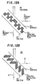
- FIGS.12A and 12B show compositions of the hologram 26 in FIGS.11A and 11B.
- the hologram 26 is composed of a dielectric multilayer film 28 and a SiO2 film 27 as a hologram layer, which are formed on the oblique plane of the prism 9 with an adhesive 29 filled between them and the oblique plane of the prism 10.
- the hologram 26 may be composed of a dielectric multilayer film 31 and a SiO2 film 30 as a hologram layer, which are formed on the oblique plane of the prism 9 with an adhesive 32 filled between them and the oblige plane of the prism 10.
- the hologram 26 in FIG.12B is different from that in FIG.12A in cross-sectional forms of the SiO2 film 30 and dielectric multilayer film 31.
- the dielectric multilayer films 28 and 31 have a function that a light with 635 nm wavelength is all transmitted through and a light with 785 nm wavelength is all reflected on.
- the adhesives 29, 32 and the SiO2 films 27, 30 have like refractive indexes. By the combination of the SiO2 film 27 or 30, the dielectric multilayer film 28 or 31 and the adhesive 29 or 32, the light with 635 nm wavelength is all transmitted through and the light with 785 nm wavelength is all reflected and diffracted on.
- the hologram 26 functions an convex surface mirror to a +1st-order diffraction light.
- an incident light 12 with 635 nm wavelength which is emitted from the semiconductor laser of the module 1 and then enters the hologram 26, as shown in FIGS.12A and 12B, is all transmitted through the SiO2 film 27 or 30, dielectric multilayer film 28 or 31 and adhesive 29 or 32, then being emitted from the hologram 26.
- an incident light 13 with 785 nm wavelength which is emitted from the semiconductor laser of the module 2 and then enters the hologram 26, as shown in FIGS.12A and 12B, is reflected and diffracted as a +1st-order diffraction light by the adhesive 29 or 32 and dielectric multilayer film 28 or 31, then being emitted from the hologram 26.
- a diffraction efficiency to a +1st-order diffraction light is 40.5 % at maximum.
- FIG.12B when the SiO2 film 30 has a step-like section form, a diffraction efficiency to a +1st-order diffraction light is increased, i.e., 81 % at maximum in a four level step form and 95% at maximum in an eight level step form.
- the distance from the module 2 to the optical coupling and dividing device 3 is shorter than the distance from the module 1 to the optical coupling and dividing device 3.
- an apparent luminous point to the light with 785 nm wavelength becomes closer to the optical coupling and dividing device 3 than that to the light with 635 nm wavelength.
- the effective optical path length from the module 2 to the collimator lens 4 as to the light with 785 nm wavelength can be shorter than the effective optical path length from the module 1 to the collimator lens 4 as to the light with 635 nm wavelength.
- the optical utilization ratio in both ways in the optical coupling and dividing devices 3 shown in FIGS.11A and 11B is 100 % to 635 nm wavelength and 66 % at maximum in a four level stop form of the SiO2 film 30 or 90 % at maximum in an eight level step form of the SiO2 film 30 to 785 nm wavelength. Therefore, with respect to 635 nm wavelength, a reproduced signal from the disk 7 has a S/N ratio equal to that in an usual optical head device and a semiconductor laser of the module 1 is only required to have an output power equal to that in an usual optical head device, and the recording of the disk 7 can be performed as well as the reproducing.
- the semiconductor laser of the module 2 has an output power equal to that in an usual optical head device, the amount of light received by the optical detector of the module 2 is 66 to 90 % as compared to that of an usual optical head device, but the S/N ratio of a reproduced signal from the disk 8 is not so reduced as compared to that in an usual optical head device.
- the semiconductor laser of the module 2 is required to have an output power 1.1 to 1.5 times that in an usual optical head device. However, the requirement can be easily satisfied as compared to the conventional optical head device.
- FIGS.13A and 13B show a fourth composition of the optical coupling and dividing device 14 used in the second embodiment shown in FIG.7.
- the optical coupling and dividing device 14 is composed of a prism 9 and a prism 10 which are adhered through a hologram 33.
- an incident light 17 with 635 nm wavelength which is emitted from the semiconductor laser of the module 1 and then enters the prism 10 of the optical coupling and dividing device 14, as, shown in FIG.13A, is reflected and diffracted as a +1st-order diffraction light by the hologram 33, then being emitted from the prism 10 of the optical coupling and dividing device 14.
- an incident light 18 with 785 nm wavelength which is emitted from the semiconductor laser of the module 2 and then enters the prism 9 of the optical coupling and dividing device 14, as shown in FIG.13B, is all transmitted through the hologram 33, than being emitted from the prism 10 of the optical coupling and dividing device 14.
- FIGS.14A and 14B show compositions of the hologram 33 in FIGS.13A and 13B.
- the hologram 33 is composed of a dielectric multilayer film 35 and a SiO2 film 34 as a hologram layer, which are formed on the oblige plane of the prism 9 with an adhesive 36 filled between them and the oblique plane of the prism 10.
- the hologram 33 may be composed of a dielectric multilayer film 38 and a SiO2 film 37 as a hologram layer, which are formed on the oblique plane of the prism 9 with an adhesive 39 filled between them and the oblique plane of the prism 10.
- the hologram 33 in FIG.14B is different from that in FIG.14A in cross-sectional forms of the SiO2 film 37 and dielectric multilayer film 38.
- the dielectric multilayer films 35 and 38 have a function that a light with 635 nm wavelength is all reflected on and a light with 785 nm wavelength is all transmitted through.
- the adhesives 36, 39 and the SiO2 films 34, 37 have like refractive indexes. By the combination of the SiO2 film 34 or 37, the dielectric multilayer film 35 or 38 and the adhesive 36 or 39, the light with 635 nm wavelength is all reflected and diffracted on and the light with 785 nm wavelength is all transmitted through.
- the hologram 33 functions an concave surface mirror to a +1st-order diffraction light.
- an incident light 17 with 635 nm wavelength which is emitted from the semiconductor laser of the module 1 and then enters the hologram 33, as shown in FIGS.14A and 14B, is reflected and diffracted as a +1st-order diffraction light by the adhesive 36 or 39 and dielectric multilayer film 35 or 38, then being emitted from the hologram 33.
- an incident light 18 with 785 nm wavelength which is emitted from the semiconductor laser of the module 2 and then enters the hologram 33, as shown in FIGS.14A and 14B, is all transmitted through the SiO2 film 34 or 37, dielectric multilayer film 35 or 38 and adhesive 36 or 39, then being emitted from the hologram 33.
- a diffraction efficiency to a +1st-order diffraction light is 40.5 % at maximum.
- FIG.14B when the SiO2 film 37 has a step-like section form, a diffraction efficiency to a +1st-order diffraction light is increased, i.e., 81 % at maximum in a four level step form and 95% at maximum in an eight level step form.
- the distance from the module 1 to the optical coupling and dividing device 14 is longer than the distance from the module 2 to the optical coupling and dividing device 14.
- an apparent luminous point to the light with 635 nm wavelength becomes farther from the optical coupling and dividing device 14 than that to the light with 785 nm wavelength.
- the effective optical path length from the module 1 to the collimator lens 4 as to the light with 635 nm wavelength can be longer than the effective optical path length from the module 2 to the collimator lens 4 as to the light with 785 nm wavelength.
- the optical utilization ratio in both ways in the optical coupling and dividing devices 14 shown in FIGS.13A and 13B is 66 % at maximum in a four level step form of the SiO2 film 30 or 90 % at maximum in an eight level step form of the SiO2 film 30 to 635 nm wavelength and is 100 % to 785 nm wavelength. Therefore, with respect to 635 nm wavelength, if the semiconductor laser of the module 1 has an output power equal to that in an usual optical head device, the amount of light received by the optical detector of the module 1 is 66 to 90 % as compared to that of an usual optical head device, but the S/N ratio of a reproduced signal from the disk 7 is not so reduced as compared to that in an usual optical head device.
- the semiconductor laser of the module 1 is required to have an output power 1.1 to 1.5 times that in an usual optical head device.
- the requirement can be easily satisfied as compared to the conventional optical head device.
- a reproduced signal from the disk 8 has a S/N ratio equal to that in an usual optical head device and a semiconductor laser of the module 2 is only required to have an output power equal to that in an usual optical head device, and the recording of the disk 8 can be performed as well as the reproducing.
- FIG.15 shows a pattern of interference fringe of the hologram 26 which is used in the optical coupling and dividing device 3 shown in FIGS.11A and 11B and the hologram 33 which is used in the optical coupling and dividing device 14 shown in FIGS.13A and 13B.
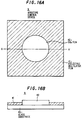
- FIGS.16A and 16B show a composition of the aperture control device 5 used in the first and second embodiments as shown in FIGS.5 and 7, where FIG.16A is a plan view thereof and FIG.16B is a sectional view cut along the A-A' line in FIG.16A.
- the aperture control device 5 is, as shown in FIGS.16A and 16B, composed of a glass substrate 40, a dielectric multilayer film 41 which is formed on the outside of a circular region in the central part of the glass substrate 40, and a SiO2 film 42 as a phase compensating film which is formed on the inside of the circular region.
- the diameter of the circular region is smaller than the effective diameters of the objective lens 6 used in the first embodiment as shown in FIG.5 and the objective lens 15 used in the second embodiment as shown in FIG.7.
- the dielectric multilayer film 41 ham a function that a light with 635 nm wavelength is all transmitted through and a light with 785 nm wavelength is all reflected on.
- the SiO2 film 42 has a function that adjusts a phase difference between a light transmitting through the dielectric multilayer film 14 on the outside of the circular region and the air and a light transmitting through the SiO2 film 42 on the inside of the circular region to be zero with respect to 635 nm wavelength.
- the light with 635 nm wavelength is all transmitted through both the outside and the inside of the circular region of the aperture control device 5.
- the light with 785 nm wavelength is all reflected on the outside of the circular region and is all transmitted through the inside of the circular region.
- FIGS.17A and 17B show another composition of the aperture control device 5 used in the first and second embodiments as shown in FIGS.5 and 7, where FIG.17A is a plan view thereof and FIG.17B is a sectional view cut along the A-A' line in FIG.17A.
- the aperture control device 5 is, as shown in FIGS.17A and 17B, composed of a glass substrate 40 on the outside of a circular region in the central part of which a SiO2 film 43 and a dielectric multilayer film 44 are formed as a diffraction grating layer, and a glass substrate 46 on the inside of the circular region of which a SiO2 film 47 is formed as a phase compensating film, which ace adhered to each other by an adhesive 45.
- the diameter of the circular region is smaller than the effective diameters of the objective lens 6 used in the first embodiment as shown in FIG.5 and the objective lens 15 used in the second embodiment as shown in FIG.7.
- the dielectric multilayer film 44 has a function that a light with 635 nm wavelength is all transmitted through and a light with 785 nm wavelength is all reflected on.
- the adhesive 45 and the SiO2 film 43 have like refractive indexes.
- the SiO2 film 47 has a function that adjusts a phase difference between a light transmitting through the SiO2 film 43, dielectric multilayer film 44 and adhesive 45 on the outside of the circular region and the air and a light transmitting through the adhesive 45 and SiO2 film 47 on the inside of the circular region to be zero with respect to 635 nm wavelength.
- the light with 635 nm wavelength is all transmitted through both the outside and the inside of the circular region of the aperture control device 5.
- the light with 785 nm wavelength is all reflected and diffracted on the outside of the circular region and is all transmitted through the inside of the circular region.
- the pattern of the SiO2, which is formed as straight lines shown in FIG.17A, may be formed as another form such as concentric circles.
- the effective numerical apertures of the objective lens 6 used in the first embodiment as shown in FIG.5 and the objective lens 15 used in the second embodiment as shown in FIG.7 are determined by the effective diameters of the objective lenses 6 and 15, respectively to the light with 635 nm wavelength and are determined by the diameter of the circular region of the aperture control device 5 shown in FIG.16A or 17A to the light with 785 nm wavelength.
- a numerical aperture as to a digital video disk can be smaller than a numerical aperture as to a compact disk, for example, the former is 0.6 and the latter is 0.45.
- the dielectric multilayer film 11 of the optical coupling and dividing device 3 shown in FIGS.6A and 6B, the dielectric multilayer film 16 of the optical coupling and dividing device 14 shown in FIGS.8A and 8B, the dielectric multilayer film 21 of the optical coupling and dividing device 14 shown in FIGS.9A and 9B, the dielectric multilayer film 25 of the optical coupling and dividing device 14 shown in FIGS.10A and 10B, the dielectric multilayer films 28, 31 of the hologram 26 shown in FIGS.12A and 12B, the dielectric multilayer films 35, 38 of the hologram 33 shown in FIGS.14A and 14B, the dielectric multilayer film 41 of the aperture control device 5 shown in FIG.16B, and the dielectric multilayer film 44 of the aperture control device 5 shown in FIG.17B can be made by forming an odd number of layers in which a high refractive index layer such as TiO2 and a low refractive index layer such as SiO2 are alternately deposited.
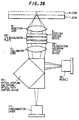
- FIG.18 shows a composition of the modules 1 and 2 used in the first and second embodiments as shown in FIGS.5 and 7.
- the module is composed of a semiconductor laser 48, an optical detector 49, a package 50 for packaging them, and an diffraction optical device 51 and an hologram optical device 52 which are disposed on the window of the package 50 with a spacer 53 inserted therebetween.
- the diffraction optical device 51 and the hologram optical device 52 have structures that SiO2 patterns are formed on glass substrates and have a function that a part of an incident light is transmitted through and a part of the incident light is diffracted on.
- a light emitted from the semiconductor laser 48 is divided into a transmitted light and a ⁇ 1st-order diffraction light by the diffraction optical device 51, each of which is by around 50% transmitted through the hologram optical device 52, then being directed to the disk.
- the two lights reflected on the disk are diffracted by around 40% as a ⁇ 1st-order diffraction light on the hologram optical device 52, being transmitted through the diffraction optical device 51, being received by the optical detector 49.
- FIG.19A shows a pattern of interference fringe of the diffraction optical device 51.
- the diffraction optical device 51 has the pattern only in a central region 54 thereof.
- the light emitted from the semiconductor laser 48 is transmitted through the inside of the region 54, and the light reflected on the disk is transmitted through the outside of the region 54.
- FIG.19B shows a pattern of interference fringe of the hologram optical device 52.
- the hologram optical device 52 has an off-axis concentric circle pattern, and it functions as a convex lens to a +1st-order diffraction light and as a concave lens to a -1st-order diffraction light.
- FIGS.20A and 20B show a pattern of light-receiving part of the optical detector 49 and locations of light spots on the light-receiving part in the case that the diffraction optical device 51 with he pattern of interference fringe shown in FIG.19A and the hologram optical device 52 with the pattern of interference fringe shown in FIG.19B are used, where FIG.20A is a plan view and FIG.20B is a side view of the central part in FIG.20A.
- the semiconductor laser 48 is disposed on the optical detector 49 through a heat sink 55. A light laterally emitted from the semiconductor laser 48 is reflected on a mirror 56, being directed upward as shown in FIG.20B.
- the +1st-order diffraction light by the hologram optical device 52 in the return way forms a light spot 67 on light-receiving parts 57 to 59 which are divided into three parts
- the -1st-order diffraction light by the hologram optical device 52 in the return way forms a light spot 68 on light-receiving parts 60 to 62 which are divided into three parts.
- the +1st-order diffraction light by the diffraction optical device 51 in the forward way forms light spots 69, 70 on light-receiving parts 63, 64, respectively
- the ⁇ 1st-order diffraction light by the hologram optical device 52 in the return way forms light spots 71, 72 on light-receiving parts 65, 66, respectively.
- the light-receiving parts 57 to 59, 63 and 65 are located behind the focusing point, and the light-receiving parts 60 to 62, 64 and 66 are located before the focusing point.
- V57 to V66 the levels of electrical signals obtained by the photoelectric conversion of the light-receiving parts 57 to 66 are represented by V57 to V66, respectively.
- a focus error signal is obtained by the operation of ⁇ (V57+V59+V61)-(V58+V60+V62) ⁇ on the known spot size method
- a track error signal is obtained by the operation of ⁇ (V63+V64)-(V65+V66) ⁇ on the known three beam method.
- a reproduction signal of the disk is obtained by the operation of (V57+V58+V59+V60+V61+V62).
- FIG.21 shows another pattern of interference fringe of the hologram optical device 52.
- the hologram optical device 52 is divided into two regions 73, 74.
- FIG.22 shown a pattern of light-receiving part of the optical detector 49 and locations of light spots on the light-receiving part in the ease that the diffraction optical device 51 with the interference fringe pattern shown in FIG.19A and the hologram optical device 52 with the interference fringe pattern shown in FIG.21 are used.
- the semiconductor laser 48 is disposed on the optical detector 49 as shown in FIG.20B.
- the +1st-order diffraction light by the region 73 of the hologram optical device 52 in the return way forms a light spot 87 on the dividing line of light-receiving parts 75, 76 which are divided into two parts
- the +1st-order diffraction light by the region 74 of the hologram optical device 52 in the return way forms a light spot 88 on the dividing line of light-receiving parts 77, 78 which are divided into two parts.
- the -1st-order diffraction light by the region 73 of the hologram optical device 52 in the return way forms a light spot 89 on the dividing line of light-receiving parts 79, 80 which are divided into two parts
- the -1st-order diffraction light by the region 74 of the hologram optical device 52 in the return way forms a light spot 90 on the dividing line of light-receiving parts 81, 82 which are divided into two parts.
- the +1st-order diffraction lights by the regions 73, 74 of the hologram optical device 52 in the return way form light spots 91, 92, respectively on a light-receiving part 83
- the -1st-order diffraction lights by the regions 73, 74 of the hologram optical device 52 in the return way form light spots 93, 94, respectively on a light-receiving part 84.
- the +1st-order diffraction lights by the regions 73, 74 of the hologram optical device 52 in the return way form light spots 95, 96, respectively on a light-receiving part 85
- the -1st-order diffraction lights by the regions 73, 74 form light spots 97, 98, respectively on a light-receiving part 86.
- a focus error signal is obtained by the operation of ⁇ (V75+V78+V79+V82)-(V76+V77+V80+V81) ⁇ on the known Foucault method
- a track error signal is obtained by the operation of ⁇ (V83+V84)-(V85+V86) ⁇ on the known three beam method.
- a reproduction signal of the disk is obtained by the operation of (V75+V76+V77+V78+V79+V80+V81+V82).
- FIG.23 An optical head device in the third preferred embodiment will be explained in FIG.23, wherein like parts are indicated by like reference numerals as used in FIG.5.
- both a module 99 and a module 100 include a semiconductor laser and an optical detector which receives light reflected on a disk.
- the semiconductor laser of the module 99 emits light with 635 nm wavelength
- the semiconductor laser of the module 100 emits light with 785 nm wavelength.
- Light emitted from the semiconductor laser of the module 99 is transmitted through a 1/2 wavelength plate 101, an optical coupling and dividing device 3, a collimator lens 4, a polarization hologram optical device 102, a 1/4 wavelength plate 103 and an aperture control device 5, entering an objective lens 6 as a collimated light, then being focused on a disk 7 such as a digital video disk with a substrate thickness of 0.6 mm.
- a disk 7 such as a digital video disk with a substrate thickness of 0.6 mm.
- Light reflected on the disk 7 is reversely transmitted through the objective lens 6, aperture control device 5 and 1/4 wavelength plate 103, being diffracted as a ⁇ diffraction light by the polarization hologram optical device 102, then being transmitted through the collimator lens 4, optical coupling and dividing device 3 and 1/2 wavelength plate 101, being received by the optical detector of the module 99.
- light emitted from the semiconductor laser of the module 100 is reflected on the optical coupling and dividing device 3, being transmitted through the collimator lens 4, polarization hologram optical device 102, 1/4 wavelength plate 103 and aperture control device 5, entering the objective lens 6 as a divergent light, then being focused on a disk 8 such as a compact disk with a substrate thickness of 1.2 mm.
- a disk 8 such as a compact disk with a substrate thickness of 1.2 mm.
- Light reflected on the disk 8 is reversely transmitted through the objective lens 6, aperture control device 5 and 1/4 wavelength plate 103, being diffracted as a ⁇ diffraction light by the polarization hologram optical device 102, then being transmitted through the collimator lens 4 and optical coupling and dividing device 3, being received by the optical detector of the module 100.
- the polarization hologram optical device 102, 1/4 wavelength plate 103 and aperture control device 5 can be integrally driven with the objective lens 6 in the directions of focusing and tracking by an actuator(not shown).
- the optical coupling and dividing device 3 has the same composition as shown in FIGS.6A and 6B, and the aperture control device 5 has the same composition as shown in FIGS.16A and 16B or FIGS.17A and 17B.
- the optical path length from the module 100 to the collimator lens 4 as to the light with 785 nm wavelength is shorter than the optical path length from the module 99 to the collimator lens 4 as to the light with 635 nm wavelength.
- the light emitted from the semiconductor laser of the module 99 is rotated by 90° polarization direction by the 1/2 wavelength plate 101, entering the polarization hologram optical device 102 as an ordinary light and all transmitted through it, then being converted from a linear polarization into a circular polarization by the 1/4 wavelength plate 103, being directed to the disk 7.
- the light reflected on the disk 7 is converted from a circular polarization into a linear polarization by the 1/4 wavelength plate 103, entering the polarization hologram optical device 102 as an extraordinary light and diffracted by 81% as a ⁇ -order diffraction light, then being received by the optical detector of the module 99.
- the light emitted from the semiconductor laser of the module 109 enters the polarization hologram optical device 102 as an ordinary light and all transmitted through it, then being converted from a linear polarization into an elliptic polarization by the 1/4 wavelength plate 103, being directed to the disk 8.
- the light reflected on the disk 8 is converted from the elliptic polarization into another elliptic polarization by the 1/4 wavelength plate 103, then entering the polarization hologram optical device 102.
- the values of ordinary and extraordinary light components of this elliptic polarization is 9%, 91%, respectively.
- by 9% of the ordinary light and by 74% of the extraordinary light are diffracted as a ⁇ -order diffraction light, being received by the optical detector of the module 100.
- the optical coupling and dividing device 3 uses the dielectric multilayer film 11 in which the light with 635 nm wavelength is all transmitted through and the light with 785 nm wavelength is all reflected on
- the optical coupling and dividing device 3 may use another dielectric multilayer film in which the light with 635 nm wavelength is all reflected on and the light with 785 nm wavelength is all transmitted through. In this case, the positions of the module 99 and module 100 need to be exchanged with each other.
- FIG.24 An optical head device in the fourth preferred embodiment will be explained in FIG.24, wherein like parts are indicated by like reference numerals as used in FIG.7.
- both a module 99 and a module 100 include a semiconductor laser and an optical detector which receives light reflected on a disk.
- the semiconductor laser of the module 99 emits light with 635 nm wavelength
- the semiconductor laser of the module 100 emits light with 785 nm wavelength.
- Light emitted from the semiconductor laser of the module 99 is reflected on an optical coupling and dividing device 14, being transmitted through a collimator lens 4, a polarization hologram optical device 105, a 1/4 wavelength plate 106 and an aperture control device 5, entering an objective lens 15 as a convergent light, then being focused on a disk 7 such as a digital video disk with a substrate thickness of 0.6 mm.
- a disk 7 such as a digital video disk with a substrate thickness of 0.6 mm.
- Light reflected on the disk 7 is reversely transmitted through the objective lens 15, aperture control device 5 and 1/4 wavelength plate 106, being diffracted as a ⁇ diffraction light by the polarization hologram optical device 105, then being transmitted through the collimator lens 4 and optical coupling and dividing device 14, being received by the optical detector of the module 99.
- light emitted from the semiconductor laser of the module 100 is transmitted through a 1/2 wavelength plate 104, the optical coupling and dividing device 14, collimator lens 4, polarization hologram optical device 105, 1/4 wavelength plate 106 and aperture control device 5, entering an objective lens 15 as a collimated light, then being focused on a disk 8 such as a compact disk with a substrate thickness of 1.2 mm.
- a disk 8 such as a compact disk with a substrate thickness of 1.2 mm.
- Light reflected on the disk 8 is reversely transmitted through the objective lens 15, aperture control device 5 and 1/4 wavelength plate 106, being diffracted as a ⁇ diffraction light by the polarization hologram optical device 105, then being transmitted through the collimator lens 4, optical coupling and dividing device 14 and 1/2 wavelength plate 102, being received by the optical detector of the module 100.
- the polarization hologram optical device 105, 1/4 wavelength plate 106 and aperture control device 5 can be integrally driven with the objective lens 15 in the directions of focusing and tracking by
- the optical coupling and dividing device 14 has the same composition as shown in FIGS.8A and 8B, and the aperture control device 5 has the same composition as shown in FIGS.16A and 16B or FIGS.17A and 17B.
- the optical path length from the module 99 to the collimator lens 4 as to the light with 635 nm wavelength is longer than the optical path length from the module 100 to the collimator lens 4 as to the light with 785 nm wavelength.
- the light emitted from the semiconductor laser of the module 99 enters the polarization hologram optical device 105 as an ordinary light and all transmitted through it, then being converted from a linear polarization into an elliptic polarization by the 1/4 wavelength plate 106, being directed to the disk 7.
- the light reflected on the disk 7 is converted from the elliptic polarization into another elliptic polarization by the 1/4 wavelength plate 106, then entering the polarization hologram optical device 105.
- the values of ordinary and extraordinary light components of this elliptic polarization is 13%, 87%, respectively.
- by 13% of the ordinary light and by 70% of the extraordinary light are diffracted as a ⁇ -order diffraction light, being received by the optical detector of the module 99.
- the light emitted from the semiconductor laser of the module 100 is rotated by 90° polarization direction by the 1/2 wavelength plate 104, entering the polarization hologram optical device 105 as an ordinary light and all transmitted through it, then being converted from a linear polarization into a circular polarization by the 1/4 wavelength plate 106, being directed to the disk 8.
- the light reflected on the disk 8 is converted from a circular polarization into a linear polarization by the 1/4 wavelength plate 106, entering the polarization hologram optical device 105 as an extraordinary light and diffracted by 81% as a ⁇ -order diffraction light, then being received by the optical detector of the module 100.
- the optical coupling and dividing device 14 uses the dielectric multilayer film 16 in which the light with 635 nm wavelength is all reflected on and the light with 785 nm wavelength is all transmitted through
- the optical coupling and dividing device 14 may use another dielectric multilayer film in which the light with 635 nm wavelength is all transmitted through and the light with 785 nm wavelength is all reflected on. In this case, the positions of the module 99 and module 100 need to be exchanged with each other.
- FIG.25 shows a composition of the modules 99 and 100.
- the module is composed of a semiconductor laser 107, an optical detector 108 and a package 50 for packaging them.
- the light emitted from the semiconductor laser 107 is transmitted through the polarization hologram optical device 102 or 105, being directed to the disk.
- the light reflected on the disk is diffracted as a ⁇ -order diffraction light by the polarization hologram optical device 102 or 105, being received by the optical detector 108.
- FIG.26A shows a pattern of interference fringe of the polarization hologram optical devices 102, 105
- FIG.26B is a sectional view thereof.
- the polarization hologram optical devices 102, 105 are a structure that a pattern of proton exchanging region and Nb205 111 is formed on a lithium niobate substrate 109 which has a birefringence characteristic.
- the interference fringe pattern of the polarization hologram optical devices 102, 105 is, as shown in FIG.26A, divided into four regions 112 to 115. Each of the regions has an off-axis concentric circle pattern.
- the regions 112, 115 function as a convex lens to a ⁇ -order diffraction light and as a concave lens to -1st-order diffraction light
- the regions 113, 114 function as a concave lens to a +1st-order diffraction light and as a convex lens to -1st-order diffraction light.
- the optical axes of the polarization hologram optical devices 102, 105 are set in the directions of X, Y as shown in FIG.26A.
- FIG.27 shows a pattern of light-receiving part of the optical detector 108 and locations of light spots on the light-receiving part in the case that the polarization hologram optical device 102 or 105 with the interference fringe pattern shown in FIGS.26A is used.
- the semiconductor laser 107 is disposed on the optical detector 108 as shown in FIG.20B.
- the +1st-order diffraction light by the region 112 of the polarization hologram optical device 102 or 105 forms a light spot 128 on the dividing line of light-receiving parts 116, 117 which are divided into two parts, and the -1st-order diffraction light by the region 112 forms a light spot 132 on a light-receiving part 124.
- the +1st-order diffraction light by the region 113 of the polarization hologram optical device 102 or 105 forms a light spot 129 on the dividing line of light-receiving parts 118, 119 which are divided into two parts, and the -1st-order diffraction light by the region 113 forms a light spot 133 on a light-receiving part 125.
- the +1st-order diffraction light by the region 114 of the polarization hologram optical device 102 or 105 forms a light spot 130 on the dividing line of light-receiving parts 120, 121 and the -1st-order diffraction light by the region 114 forms a light spot 134 on a light-receiving part 126.
- the +1st-order diffraction light by the region 115 of the polarization hologram optical device 102, 105 forms a light spot 131 on the dividing line of light-receiving parts 122, 123 and the -1st-order diffraction light by the region 115 forms a light spot 135 on a light-receiving part 127.
- the light-receiving parts 116, 117, 122, 123, 125 and 126 are located behind the focusing point, and the light-receiving parts 118, 119, 120, 121, 124 and 127 are located before the focusing point.
- a focus error signal is obtained by the operation of ⁇ (V116+V118+V121+V123)-(V117+V119+V120+V122) ⁇ on the known spot size method
- a track error signal is obtained by the operation of ⁇ (V124+V126)-(V125+V127) ⁇ on the known push-pull method.
- a reproduction signal of the disk is obtained by the operation of (V124+V125+V126+V127).
- the track error signal is also obtained by the simple-holding of ⁇ (V124+V126)-(V125+V127) ⁇ at a filling point and a rising point of the reproduction signal of the disk on the known heterodyne method.
- FIG.28 shows another pattern of interference fringe of the polarization hologram optical devices 102, 105.
- the interference fringe pattern of the polarization hologram optical devices 102, 105 is, as shown in FIG.28, divided into four regions 136 to 139.
- the optical axes of the polarization hologram optical devices 102, 105 are set in the directions of X, Y as shown in FIG.28.
- FIG.29 shows a pattern of light-receiving part of the optical detector 108 and locations of light spots on the light-receiving part in the case that the polarization hologram optical device 102 or 105 with the interference fringe pattern shown in FIGS.28 is used.
- the semiconductor laser 107 is disposed on the optical detector 108 as shown in FIG.20B.
- the +1st-order diffraction light by the region 136 of the polarization hologram optical device 102 or 105 forms a light spot 152 on the dividing line of light-receiving parts 140, 141 which are divided into two parts, and the -1st-order diffraction light by the region 136 forms a light spot 156 on a light-receiving part 148.
- the +1st-order diffraction light by the region 137 of the polarization hologram optical device 102 or 105 forms a light spot 153 on the dividing line of light-receiving parts 142, 143 which are divided into two parts, and the -1st-order diffraction light by the region 137 forms a light spot 157 on a light-receiving part 149.
- the +1st-order diffraction light by the region 138 of the polarization hologram optical device 102 or 105 forms a light spot 154 on the dividing line of light-receiving parts 144, 145 and the -1st-order diffraction light by the region 138 forms a light spot 158 on a light-receiving part 150.
- the +1st-order diffraction light by the region 139 of the polarization hologram optical device 102, 105 forms a light spot 155 on the dividing line of light-receiving parts 146, 147 and the -1st-order diffraction light by the region 139 forms a light spot 159 on a light-receiving part 151.
- a focus error signal is obtained by the operation of ⁇ (V140+V142+V145+V147)-(V141+V143+V144+V146) ⁇ on the known Foucault method
- a track error signal is obtained by the operation of ⁇ (V148+V150)-(V149+V151) ⁇ on the known push-pull method.
- a reproduction signal of the disk is obtained by the operation of (V148+V149+V150+V151).
- the track error signal is also obtained by the sample-holding of ⁇ (V148+V151)-(V149+V150) ⁇ at a falling point and a rising point of the reproduction signal of the disk on the known heterodyne method.
- the two modules which include the semiconductor laser and optical detector are used to miniaturize the size, two pairs of blocks, in each pair of blocks a semiconductor laser and an optical detector being separately included, may be used.
- a module 100 includes a semiconductor laser and an optical detector which receives light reflected on a disk.
- a semiconductor laser 160 emits light with 635 nm wavelength, and the semiconductor laser of the module 100 emits light with 785 nm wavelength.
- Light emitted from the semiconductor laser 160 is transmitted through an optical coupling and dividing/optical path control device 161, a collimator lens 4, a polarization hologram optical device 102, a 1/4 wavelength plate 103 and an aperture control device 5, entering an objective lens 6 as a collimated light, then being focused on a disk 7 such as a digital video disk with a substrate thickness of 0.6 mm.
- light emitted from the semiconductor laser of the module 100 is reflected by the optical coupling and dividing/optical path control device 161, then being transmitted through the collimator lens 4, polarization hologram optical device 102, 1/4 wavelength plate 103 and aperture control device 5, entering the objective lens 6 as a divergent light, then being focused on a disk 8 much as a compact disk with a substrate thickness of 1.2 mm.
- Light reflected on the disk 8 is reversely transmitted through the objective lens 6, aperture control device 5 and 1/4 wavelength plate 103, being diffracted as a ⁇ diffraction light by the polarization hologram optical device 102, then being reversely transmitted through the collimator lens 4 and optical coupling and dividing/optical path control device 161, being received by the optical detector of the module 100.
- the polarization hologram optical device 102, 1/4 wavelength plate 103 and aperture control device 5 can be integrally driven with the objective lens 6 in the directions of focusing and tracking by an actuator(not shown).
- the aperture control device 5 has the same composition as shown in FIGS.16A, 16B or FIGS.17A, 17B.
- the polarization hologram optical device 102 and 1/4 wavelength plate 103 function as those in the third embodiment as shown in FIG.23.
- FIGS.31A to 31C show a composition of the optical coupling and dividing/optical path control device 161 used in the fifth embodiment as shown in FIG.30.
- the optical coupling and dividing/optical path control device 161 is composed of prisms 162, 163 and 164, which are adhered through dielectric multilayer films 165, 166.
- the dielectric multilayer film 165 has a function that, of an incident light with 635 nm wavelength, a P-polarization component is all transmitted through and a S-polarization component is all reflected on.
- the dielectric multilayer film 166 has a function that a light with 635 nm wavelength is all transmitted through and a light with 785 nm wavelength is all reflected on.
- An incident light 168 with 635 nm wavelength which is emitted from the semiconductor laser 160 and then enters the prism 162 of the optical coupling and dividing/optical path control device 161, as shown in FIG.31A, is projected as a P-polarized light onto the dielectric multilayer film 165 and all transmitted through it, further being all transmitted through the dielectric multilayer film 166, then being emitted from the prism 164 of the optical coupling and dividing/optical path control device 161.
- a incident light 169 with 635 nm wavelength which is reflected by the disk 7 and then enters the prism 164 of the optical coupling and dividing/optical path control device 161, as shown in FIG.31B, is all transmitted through the dielectric multilayer film 166 and projected as a S-polarized light onto the dielectric multilayer film 165 and is all reflected on it, being all reflected by a reflection film 167, again being transmitted through the dielectric multilayer film 166, then being emitted from the prism 164 of the optical coupling and dividing/optical path control device 161.
- an incident light 170 with 785 nm wavelength which is emitted from the semiconductor laser of the module 100 and then enters the prism 164 of the optical coupling and dividing/optical path control device 161, as shown in FIG.31C, is all reflected by the dielectric multilayer film 166, then being emitted from the prism 164.
- An incident light with 785 nm wavelength which is reflected by the disk 8 and then enters the prism 164 of the optical coupling and dividing/optical path control device 161, reversely passes through the same path as the incident light 170, being emitted from the prism 164.
- FIG.32 An optical head device in the sixth preferred embodiment will be explained in FIG.32.
- the optical coupling and dividing/optical path control device 161 used in the fifth embodiment as shown in FIG.30 is replaced by an optical coupling and dividing/optical path control device 171.
- FIGS.33A to 33C show a composition of the optical coupling and dividing/optical path control device 171.
- the optical coupling and dividing/optical path control device 171 is composed of prisms 172, 173 and 174, which are adhered through dielectric multilayer films 175, 176.
- the dielectric multilayer film 175 has a function that, of an incident light with 635 nm wavelength, a P-polarization component is all transmitted through and a S-polarization component is all reflected on.
- the dielectric multilayer film 176 has a function that a light with 635 nm wavelength is all transmitted through and a light with 785 nm wavelength is all reflected on.
- An incident light 168 with 635 nm wavelength which is emitted from the semiconductor laser 160 and then enters the prism 172 of the optical coupling and dividing/optical path control device 171, as shown in FIG.33A, is projected as a P-polarized light onto the dielectric multilayer film 175 and all transmitted through it, further being all transmitted through the dielectric multilayer film 176, then being emitted from the prism 174 of the optical coupling and dividing/optical path control device 171.
- an incident light 169 with 635 nm wavelength which is reflected by the disk 7 and then enters the prism 174 of the optical coupling and dividing/optical path control device 171, as shown in FIG.33B, is all transmitted through the dielectric multilayer film 176 and projected as a S-polarized light onto the dielectric multilayer film 175 and is all reflected on it, being totally reflected two times on boundary surfaces of the prism 173 and the air, again being all transmitted through the dielectric multilayer film 176, then being emitted from the prism 174 of the optical coupling and dividing/optical path control device 171.
- an incident light 170 with 785 nm wavelength which is emitted from the semiconductor laser of the module 100 and then enters the prism 174 of the optical coupling and dividing/optical path control device 171, as shown in FIG.33C, is all reflected by the dielectric multilayer film 176, then being emitted from the prism 174.
- An incident light with 785 nm wavelength which is reflected by the disk 8 and then enters the prism 174 of the optical coupling and dividing/optical path control device 171, reversely passes through the same path as the incident light 170, being emitted from the prism 174.
- the distance from the module 100 to the optical coupling and dividing/optical path control device 161 or 171 is shorter than the distance from the semiconductor laser 160 to the optical coupling and dividing/optical path control device 161 or 171.
- the effective optical path length from the semiconductor laser 160 to the collimator lens 4 as to the light with 635 nm wavelength can be equal to the effective optical path length from the module 100 to the collimator lens 4 as to the light with 635 nm wavelength, and the effective optical path length from the module 100 to the collimator long 4 as to the light with 785 nm wavelength can be shorter than these effective optical path lengths.
- a module 99 includes a semiconductor loser and an optical detector which receives light reflected on a disk.
- the semiconductor laser of the module 99 emits light with 635 nm wavelength, and a semiconductor laser 177 emits light with 785 nm wavelength.
- Light emitted from the semiconductor laser of the module 99 is reflected by an optical coupling and dividing/optical path control device 178, being transmitted through a collimator lens 4, a polarization hologram optical device 105, a 1/4 wavelength plate 106 and an aperture control device 5, entering an objective lens 15 as a convergent light, then being focused on a disk 7 such as a digital video disk with a substrate thickness of 0.6 mm.
- light emitted from the semiconductor laser 177 is transmitted through the optical coupling and dividing/optical path control device 178, collimator lens 4, polarization hologram optical device 105, 1/4 wavelength plate 106 and aperture control device 5, entering the objective lens 15 as a collimated light, then being focused on a disk 8 such as a compact disk with a substrate thickness of 1.2 mm.
- Light reflected on the disk 8 is reversely transmitted through the objective lens 15, aperture control device 5 and 1/4 wavelength plate 106, being diffracted as a ⁇ diffraction light by the polarization hologram optical device 105, then being reversely transmitted through the collimator lens 4, being reflected by the optical coupling and dividing/optical path control device 178, being received by the optical detector of the module 99.
- the polarization hologram optical device 105, 1/4 wavelength plate 106 and aperture control device 5 can be integrally driven with the objective lens 15 in the directions of focusing and tracking by an actuator(not shown).
- the aperture control device 5 has the same composition as shown in FIGS.16A, 16B or FIGS.17A, 17B.
- the polarization hologram optical device 105 and 1/4 wavelength plate 106 function as those in the fourth embodiment as shown in FIG.24.
- FIGS.35A to 35C show a composition of the optical coupling and dividing/optical path control device 178 used in the seventh embodiment as shown in FIG.34.
- the optical coupling and dividing/optical path control device 178 is composed of prisms 162, 163 and 164, which are adhered through dielectric multilayer films 179, 180.
- the dielectric multilayer film 179 has a function that a light with 635 nm wavelength is all reflected on and a light with 785 nm wavelength is all transmitted through.
- the dielectric multilayer film 180 has a function that a light with 635 nm wavelength is all transmitted through and, of an incident light with 785 nm wavelength, a P-polarization component is all transmitted through and a S-polarization component is all reflected on.
- An incident light 181 with 635 nm wavelength which is emitted from the semiconductor laser of the module 99 and than enters the prism 164 of the optical coupling and dividing/optical path control device 178, as shown in FIG.35A, is all transmitted through a dielectric multilayer film 180, being all reflected by a reflection film of the prism 163 and the dielectric multilayer film 179, again being transmitted through the dielectric multilayer film 180, then being emitted from the prism 164.
- An incident light with 635 nm wavelength which is reflected by the disk 7 and then enters the prism 164 of the optical coupling and dividing/optical path control device 178, reversely passes through the same path as the incident light 181, being emitted from the prism 164 of the optical coupling and dividing/optical path control device 178.
- an incident light 182 with 785 nm wavelength which is emitted from the semiconductor laser 177 and then enters the prism 162 of the optical coupling and dividing/optical path control device 178, as shown in FIG.33B, is all transmitted through the dielectric multilayer film 179, further being projected as a P-polarized light onto the dielectric multilayer film 180 and all transmitted through it, then being emitted from the prism 164.
- an incident light 183 with 785 nm wavelength which is reflected by the disk 8 and then enters the prism 164 of the optical coupling and dividing/optical path control device 178, as shown in FIG.33C, is projected as a S-polarized light onto the dielectric multilayer film 180 and is all reflected on it, then being emitted from the prism 164.
- FIG.36 An optical head device in the eighth preferred embodiment will be explained in FIG.36.
- the optical coupling and dividing/optical path control device 178 used in the seventh embodiment as shown in FIG.34 in replaced by an optical coupling and dividing/optical path control device 184.
- FIGS.37A to 37C show a composition of the optical coupling and dividing/optical path control device 184.
- the optical coupling and dividing/optical path control device 184 is composed of prisms 172, 173 and 174, which are adhered through dielectric multilayer films 185, 186.
- the dielectric multilayer film 185 has a function that a light with 635 nm wavelength is all reflected on and a light with 785 nm wavelength is all transmitted through.
- the dielectric multilayer film 186 has a function that a light with 635 nm wavelength is all transmitted through and, of an incident light with 785 nm wavelength, a P-polarization component is all transmitted through and a S-polarization component is all reflected on.
- An incident light 181 with 635 nm wavelength which is emitted from the semiconductor laser of the module 99 and then enters the prism 174 of the optical coupling and dividing/optical path control device 184, as shown in FIG.37A, is all transmitted through the dielectric multilayer film 186, being totally reflected two times on boundary surfaces of the prism 173 and the air, then being reflected by the dielectric multilayer film 185, again being all transmitted through the 186, being emitted from the optical coupling and dividing/optical path control device 184.
- the light with 635 nm wavelength which is reflected by the disk 7 and then enters the prism 174 of the optical coupling and dividing/optical path control device 184, reversely passes through the lame path a: the incident light 181, being emitted from the prism 174 of the optical coupling and dividing/optical path control device 184.
- an incident light 182 with 785 nm wavelength which is emitted from the semiconductor laser 177 and then enters the prism 172 of the optical coupling and dividing/optical path control device 184, as shown in FIG.33B, is all transmitted through the dielectric multilayer films 185 and the prism 173, being projected as a P-polarized light onto the dielectric multilayer film 186 and all transmitted through it, then being emitted from the prism 174 of the optical coupling and dividing/optical path control device 184.
- an incident light with 785 nm wavelength which is reflected by the disk 8 and then enters the prism 174 of the optical coupling and dividing/optical path control device 184, as shown in FIG.37C, is projected as a S-polarized light onto the dielectric multilayer film 186 and is all reflected on it, then being emitted from the prism 174.
- the distance from the semiconductor laser 177 to the optical coupling and dividing/optical path control device 178 or 184 is equal to the distance from the module 99 to the optical coupling and dividing/optical path control device 178 or 184.
- the effective optical path length from the semiconductor laser 177 to the collimator lens 4 as to the light with 785 nm wavelength can be equal to the effective optical path length from the module 99 to the collimator lens 4 as to the light with 785 nm wavelength, and the effective optical path length from the module 99 to the collimator lens 4 as to the light with 635 nm wavelength can be longer than these effective optical path lengths.
- FIGS.38A to 38C show another composition of optical coupling and dividing/optical path control device 161 used in the fifth embodiment as shown in FIG.30.
- the optical coupling and dividing/optical path control device 161 is composed of prisms 9, 10 which are adhered through a hologram 187.
- An incident light 168 with 635 nm wavelength which is emitted from the semiconductor laser 160 and then enters the prism 9 of the optical coupling and dividing/optical path control device 161, as shown in FIG.38A, is projected as a P-polarization light onto the hologram 187 and all transmitted through it, being emitted from the optical coupling and dividing/optical path control device 161.
- an incident light 169 with 635 nm wavelength which is reflected by the disk 7 and then enters the prism 10 of the optical coupling and dividing/optical path control device 161, as shown in FIG.38B, is projected as a S-polarization light onto the hologram 187, thereby being reflected and diffracted as a +1st-order diffraction light, being emitted from the optical coupling and dividing/optical path control device 161.
- an incident light 170 with 785 nm wavelength which is emitted from the semiconductor laser of the module 100 and then enters the prism 10 of the optical coupling and dividing/optical path control device 161, as shown in FIG.38C, is all reflected by the hologram 187, being emitted from the prism 10.
- the light with 785 nm wavelength which is reflected by the disk 8 and then enters the prism 10 of the optical coupling and dividing/optical path control device 161, reversely passing through the same path as the incident light 170, being emitted from the prism 10.
- FIGS.39A and 39B show compositions of the hologram 187 shown in FIGS.38A to 38C.
- the hologram 187 is, as shown in FIG.39A, composed of a SiO2 film 188 as a hologram layer, a dielectric multilayer film 189 which are formed on the oblique plane of the prism 9, a dielectric multilayer film 191 which is formed on the oblique plane of the prism 10, and an adhesive 190 filled therebetween.
- the hologram 187 may be composed of a SiO2 film 192 as a hologram layer, a dielectric multilayer film 193 which are formed on the oblique plane of the prism 9, a dielectric multilayer film 195 which is formed on the oblique plane of the prism 10, and an adhesive 194 filled therebetween.
- the dielectric multilayer films 189 and 193 have a function that, of a light with 635 nm wavelength, a P-polarization component is all transmitted through and a S-polarization component is all reflected on.
- the dielectric multilayer films 191 and 195 have a function that a light with 635 nm wavelength is all transmitted through and a light with 785 nm wavelength is all reflected on.
- the adhesives 190, 194 and the SiO2 films 188, 192 have like refractive indexes.
- the hologram 187 functions an concave surface mirror to a +1st-order diffraction light.
- an incident light 168 with 635 nm wavelength which is emitted from the semiconductor laser 160 and then enters the hologram 187, as shown in FIGS.39A and 39B, is projected as a P-polarization light onto the SiO2 film 188 or 192, dielectric multilayer film 189 or 193 and adhesive 190 or 194 and all transmitted through them, then being transmitted through the dielectric multilayer film 191 or 195, being emitted from the hologram 187.
- An incident light 169 which is reflected on the disk 7 and then enters the hologram 187, is all transmitted through the dielectric multilayer film 191 or 195 and is then projected as a S-polarization light onto the adhesive 190 or 194 and dielectric multilayer film 189 or 193, being reflected and diffracted as a +1st-order diffraction light, again being all transmitted through the dielectric multilayer film 191 or 195, being emitted from the hologram 187.
- an incident light 170 with 785 nm wavelength which is emitted from the semiconductor laser of the module 100 and then enters the hologram 187, is all reflected on the dielectric multilayer film 191 or 195, then being emitted from the hologram 187.
- a diffraction efficiency to a +1st-order diffraction light is 40.5 % at maximum.
- FIG.39B when the SiO2 film 192 has a step-like section form, a diffraction efficiency to a +1st-order diffraction light is increased, i.e., 81 % at maximum in a four level step form and 95% at maximum in an eight level step form.
- the distance from the module 100 to the optical coupling and dividing/optical path control device 161 is shorter than the distance from the semiconductor laser 160 to the optical coupling and dividing/optical path control device 161.
- the optical coupling and dividing/optical path control device 161 as shown in FIGS.38A to 38C a focused point to the light with 635 nm wavelength reflected on the disk 7 becomes closer to the optical coupling and dividing/optical path control device 161 than that to the light with 785 nm wavelength reflected on the disk 8.
- the effective optical path length from the semiconductor laser 160 to the collimator lens 4 as to the light with 635 nm wavelength can be equal to the effective optical path length from the module 100 to the collimator lens 4 as to the light with 635 nm wavelength, and the effective optical path length from the module 100 to the collimator lens 4 as to the light with 785 nm wavelength can be shorter than these effective optical path lengths.
- FIGS.40A to 40C show another composition of the optical coupling and dividing/optical path control device 178 used in the seventh embodiment as shown in FIG.34.
- This optical coupling and dividing/optical path control device 178 is, as shown in FIGS.40A to 40C, composed of prisms 9, 10 which are adhered through a hologram 196.
- An incident light 181 with 635 nm wavelength which is emitted from the semiconductor laser of the module 99 and then enters the prism 10 of the optical coupling and dividing/optical path control device 178, as shown in FIG.40A, is reflected and diffracted as a +1st-order diffraction light by the hologram 196, being emitted from the prism 10.
- the light with 635 nm wavelength which is reelected on the disk 7 and enters the prism 10 of the optical coupling and dividing/optical path control device 178, reversely passes through the same path as the incident light, being emitted from the prism 10.
- an incident light with 785 nm wavelength which is emitted from the semiconductor laser 177 and then enters prism 9 of the optical coupling and dividing/optical path control device 178, as shown in FIG.40B, is projected as a P-polarization light onto the hologram 196 and all transmitted through it, then being transmitted through the prism 10, being emitted from the hologram 187.
- An incident light 183 which is reflected on the disk 8 and then enters the prism 10 of the optical coupling and dividing/optical path control device 178, as shown in FIG.40C, is projected as a S-polarization light onto the hologram 196 and is all reflected on it, being emitted from the prism 10.
- FIGS.41A and 41B show compositions of the hologram 196 shown in FIGS.40A to 40C.
- the hologram 196 is, as shown in FIG.41A, composed of a SiO2 film 197 as a hologram layer, a dielectric multilayer film 198 which are formed on the oblique plane of the prism 9, a dielectric multilayer film 200 which is formed on the oblique plane of the prism 10, and an adhesive 199 filled therebetween.
- the hologram 196 may be composed of a SiO2 film 201 as a hologram layer, a dielectric multilayer film 202 which are formed on the oblique plane of the prism 9, a dielectric multilayer film 204 which is formed on the oblique plane of the prism 10, and an adhesive 203 filled therebetween.
- the dielectric multilayer films 198 and 202 have a function that a light with 635 nm wavelength is all reflected on and a light with 785 nm wavelength is all transmitted through.
- the dielectric multilayer films 200 and 204 have a function that a light with 635 nm wavelength is all transmitted through and, of a light with 785 nm wavelength, a P-polarization component is all transmitted through and a S-polarization component is all reflected on.
- the adhesives 199, 203 and the SiO2 films 197, 201 have like refractive indexes.
- the hologram 196 functions an concave surface mirror to a +1st-order diffraction light.
- an incident light 181 with 635 nm wavelength which is emitted from the semiconductor laser of the module 99 and then enters the hologram 196, as shown in FIGS.41A and 41B, is all transmitted through the dielectric multilayer film 200 or 204, being reflected and diffracted as a +1st-order diffraction light by the adhesive 199 or 203 and dielectric multilayer film 198 or 202, again being all transmitted through the dielectric multilayer film 200 or 204, being emitted from the hologram 196.
- the light with 635 nm wavelength which is reflected on the disk 7 and then enters the hologram 196, reversely passes through the same path as the incident light 181, being emitted from the hologram 196.
- an incident light 182 with 785 nm wavelength which is emitted from the semiconductor laser 177 and then enters the hologram 196, as shown in FIGS.41A and 41B, is all transmitted through the SiO2 film 197 or 201, the dielectric multilayer film 198 or 202 and the adhesive 199 or 203, then being projected as a P-polarization light onto the dielectric multilayer film 200 or 204 and all transmitted through it, then being emitted from the hologram 196.
- a diffraction efficiency to a +1st-order diffraction light is 40.5 % at maximum.
- FIG.41B when the SiO2 film 201 has a step-like section form, a diffraction efficiency to a +1st-order diffraction light is increased, i.e., 81 % at maximum in a four level step form and 95% at maximum in an eight level stop form.
- the distance from the semiconductor laser 177 to the optical coupling and dividing/optical path control device 178 is equal to the distance from the semiconductor laser of the module 99 to the optical coupling and dividing/optical path control device 178.
- a focused point to the light with 635 nm wavelength reflected on the disk 7 becomes closer to the optical coupling and dividing/optical path control device 178 than that to the light with 785 nm wavelength reflected on the disk 8.
- the effective optical path length from the semiconductor laser 177 to the collimator lens 4 as to the light with 785 nm wavelength can be equal to the effective optical path length from the module 99 to the collimator lens 4 as to the light with 785 nm wavelength, and the effective optical path length from the module 99 to the collimator lens 4 as to the light with 635 nm wavelength can be longer than these effective optical path lengths.
- the lens system composed of the collimator lens 4 and objective lens 6 is used, a lens system composed of only an objective lens may be used therein. Also, though, in the respective embodiments as shown in FIGS. 7, 27, 34, 36, the lens system composed of the collimator lens 4 and objective lens 6 is used, a lens system composed of only an objective lens may be used therein.
- a module 100 includes a semiconductor laser and an optical detector which receives light reflected on a disk.
- a semiconductor laser 160 emits light with 635 nm wavelength, and the semiconductor laser of the module 100 emits light with 785 nm wavelength.
- Light emitted from the semiconductor laser 160 is transmitted through a collimator lens 205, an optical coupling and dividing device 206, a polarization hologram optical device 102, a 1/4 wavelength plate 103 and an aperture control device 5, entering an objective lens 6 as a collimated light, then being focused on a disk 7 such as a digital video disk with a substrate thickness of 0.6 mm.
- light emitted from the semiconductor laser of the module 100 is transmitted through the collimator lens 4, then being reflected by the optical coupling and dividing device 206, being transmitted through the polarization hologram optical device 102, 1/4 wavelength plate 103 and aperture control device 5, entering the objective lens 6 as a divergent light, then being focused on a disk 8 such as a compact disk with a substrate thickness of 1.2 mm.
- the polarization hologram optical device 102, 1/4 wavelength plate 103 and aperture control device 5 can be integrally driven with the objective lens 6 in the directions of focusing and tracking by an actuator(not shown).
- the aperture control device 5 has the same composition as shown in FIGS.16A, 16B or FIGS.17A, 17B.
- the polarization hologram optical device 102 and 1/4 wavelength plate 103 function as those in the third embodiment as shown in FIG.23.
- FIGS.43A to 43C show a composition of the optical coupling and dividing device 206 used in the ninth embodiment as shown in FIG.42.
- the optical coupling and dividing device 206 is composed of a prism 9 and a prism 10 which are adhered through a dielectric multilayer film 208.
- the dielectric multilayer film 208 has a function that, of a light with 635 nm wavelength, a P-polarization component is all transmitted through and a S-polarization component is all reflected on and a light with 785 nm wavelength is all reflected on.
- an incident light 209 with 635 nm wavelength which is emitted from the semiconductor laser 160 and then enters the prism 9 of the optical coupling and dividing device 206, is projected as a P-polarization light onto the dielectric multilayer film 208 and all transmitted through it, being emitted from the prism 10.
- an incident light 211 with 785 nm wavelength which is emitted from the semiconductor laser of the module 100 and then enters the prism 10 of the optical coupling and dividing device 206, as shown in FIG.43C, is all reflected by the dielectric multilayer film 208, then being emitted from the prism 10.
- FIGS.44A and 44B show a composition of the optical path control device 207 used in the ninth embodiment as shown in FIG.42.
- the optical path control device 207 is composed of prisms 212, 213 which are adhered through a dielectric multilayer film 214.
- the dielectric multilayer film 214 is a function that a light with 635 nm wavelength is all transmitted through and a light with 785 nm wavelength is all reflected on.
- an incident light 218 with 785 nm wavelength which is emitted from the semiconductor laser of the module 100 and then enters the prism 212 of the optical path control device 207, as shown in FIG.44B, is all reflected on the dielectric multilayer film 214, being emitted from the prism 212.
- optical head device in the tenth preferred embodiment will be explained in FIG.45.
- the optical path control device 207 in the ninth embodiment as shown in FIG.42 is replaced by an optical path control device 219.
- FIGS.46A and 46B show a composition of the optical path control device 219 used in the tenth embodiment as shown in FIG.45.
- the optical path control device 219 is composed of prisms 220, 221 which are adhered through a dielectric multilayer film 222.
- the dielectric multilayer film 222 is a function that a light with 635 nm wavelength is all transmitted through and a light with 785 nm wavelength is all reflected on.
- an incident light 218 with 785 nm wavelength which is emitted from the semiconductor laser of the module 100 and then enters the prism 220 of the optical path control device 219, is all reflected on the dielectric multilayer film 222, being emitted from the prism 220.
- the light with 785 nm wavelength which is reflected on the disk 8 and then enters the prism 220 of the optical path control device 219, reversely passes through the same path as the incident light 218, being emitted from the prism 220.
- the distance from the semiconductor laser 160 to the collimator lens 205 is equal to the focal distance of the collimator lens 205, and the distance from the module 100 to the collimator lens 4 is shorter than the focal distance of the collimator lens 4.
- the optical path control device 207 as shown in FIGS.44A and 44B or the optical path control device 219 as shown in FIGS.46A and 46B
- the effective optical path length from the module 100 to the collimator lens 4 as to 635 nm wavelength light can be equal to the focal distance of the collimator 4
- the effective optical path length from the module 100 to the collimator lens 4 as to 785 nm wavelength light can be shorter than the focal distance.
- the optical coupling and dividing device 206 uses the dielectric multilayer film 208 in which, of the light with 635 nm wavelength, the P-polarization component is all transmitted through and the S-polarization component is all reflected on and the light with 785 nm wavelength is all reflected on
- the optical coupling and dividing device 206 may use another dielectric multilayer film in which, of the light with 635 nm wavelength, the P-polarization component is all transmitted through and the S-polarization component is all reflected on and the light with 785 nm wavelength is all transmitted through.
- the positions of the block which is composed of the semiconductor laser 160 and collimator lens 205 and the block which is composed of the module 100, optical path control device 207 or 219 and collimator lens 4 need to be exchanged with each other, and the light with 635 nm wavelength emitted from the semiconductor laser 160 needs to be projected as a S-polarization light onto the dielectric multilayer film of the optical coupling and dividing device.
- a module 99 includes a semiconductor laser and an optical detector which receives light reflected on a disk.
- the semiconductor laser of the module 99 emits light with 635 nm wavelength, and a semiconductor laser 177 emits light with 785 nm wavelength.
- Light emitted from the semiconductor laser of the module 99 is reflected by an optical path control device 207, being transmitted through a collimator lens 4, being reflected by an optical coupling and dividing device 223, being transmitted through a polarization hologram optical device 105, a 1/4 wavelength plate 106 and an aperture control device 5, entering an objective lens 15 as a convergent light, then being focused on a disk 7 such as a digital video disk with a substrate thickness of 0.6 mm.
- light emitted from the semiconductor laser 177 is transmitted through the collimator lens 205, optical coupling and dividing device 223, polarization hologram optical device 105, 1/4 wavelength plate 106 and aperture control device 5, entering the objective lens 15 as a collimated light, then being focused on a disk 8 such as a compact disk with a substrate thickness of 1.2 mm.
- the polarization hologram optical device 105, 1/4 wavelength plate 106 and aperture control device 5 can be integrally driven with the objective lens 15 in the directions of focusing and tracking by an actuator(not shown).
- the aperture control device 5 has the same composition as shown in FIGS.16A, 16B or FIGS.17A, 17B.
- the polarization hologram optical device 105 and 1/4 wavelength plate 106 function as those in the fourth embodiment as shown in FIG.24.
- FIGS.48A to 48C show a composition of the optical coupling and dividing device 223 used in the eleventh embodiment as shown in FIG. 47.
- the optical coupling and dividing device 223 is composed of a prism 9 and a prism 10 which are adhered through a dielectric multilayer film 224.
- the dielectric multilayer film 224 has a function that a light with 635 nm wavelength is all reflected on and, of a light with 785 nm wavelength, a P-polarization component is all transmitted through and a S-polarization component is all reflected on
- an incident light 225 with 635 nm wavelength which is emitted from the semiconductor laser of the module 99 and then enters the prism 10 of the optical coupling and dividing device 223, is all reflected on the dielectric multilayer film 224, being emitted from the prism 10.
- an incident light 226 with 785 nm wavelength which is emitted from the semiconductor laser 177 and then enters the prism 9 of the optical coupling and dividing device 223, as shown in FIG.48B, is projected as a P-polarization light onto the dielectric multilayer film 224 and all transmitted through it, being emitted from the prism 10.
- An incident light 227 with 785 nm wavelength, which is reflected on the disk 8 and then enters prism 10 of the optical coupling and dividing device 223, as shown in FIG.48C is projected as a S-polarization light onto the dielectric multilayer film 224 and all reflected on it, being emitted from the prism 10.
- optical path control device 207 in the eleventh embodiment as shown in FIG.47 is replaced by an optical path control device 219.
- the optical path control device 207 used in the eleventh embodiment as shown in FIG.47 has the same composition as the optical path control device 207 as shown in FIGS.44A and 44B
- the optical path control device 219 used in the twelfth embodiment has the same composition as the optical path control device 219 as shown in FIGS. 46A and 46B.
- the distance from the semiconductor laser 177 to the collimator lens 205 is equal to the focal distance of the collimator lens 205, and the distance from the module 99 to the collimator lens 4 is equal to the focal distance of the collimator lens 4.
- the effective optical path length from the module 99 to the collimator lens 4 as to 785 nm wavelength light can be equal to the focal distance of the collimator 4, and the effective optical path length from the module 99 to the collimator lens 4 as to 635 nm wavelength light can be longer than the focal distance.
- the optical coupling and dividing device 223 uses the dielectric multilayer film 224 in which the light with 635 nm wavelength is all reflected on and, of the light with 785 nm wavelength, the P-polarization component is all transmitted through and the S-polarization component is all reflected on
- the optical coupling and dividing device 223 may use another dielectric multilayer film in which the light with 635 nm wavelength is all transmitted through and, of the light with 785 nm wavelength, the P-polarization component is all transmitted through and the S-polarization component is all reflected on.
- the positions of the block which is composed of the semiconductor laser 177 and collimator lens 205 and the block which is composed of the module 99, optical path control device 207 or 219 and collimator lens 4 need to be exchanged with each other, and the light with 785 nm wavelength emitted from the semiconductor laser 177 needs to be projected as a S-polarization light onto the dielectric multilayer film of the optical coupling and dividing device.
- FIGS.50A and 50B show another composition of the optical path control device 207 used in the ninth embodiment as shown in FIG.42.
- This optical path control device 207 is, as shown in FIGS.50A and 50B, composed of a prism 9 and a hologram 228 which is on the oblique plane of the prism 9.
- an incident light 217 with 635 nm wavelength which is reflected on the disk 7 and then enters the prism 9 of the optical path control device 207, is reflected and diffracted as a +1st-order diffraction light by the hologram 228, being emitted from the prism 9.
- an incident light 218 with 785 nm wavelength which is emitted from the semiconductor laser of the module 100 and then enters the prism 9 of the optical path control device 207, is all reflected by the hologram 228, being emitted from the prism 9.
- FIGS.51A and 51B show compositions of the hologram 228 in FIGS.50A and 50B.
- the hologram 228 is, as shown in FIG.51A, composed of a dielectric multilayer film 229 and a SiO2 film 230 as a hologram layer which are formed on the oblique plane of the prism 9.
- the hologram 228 may be, as shown in FIG.51B, composed of a dielectric multilayer film 231 and a SiO2 film 232 as a hologram layer which are formed on the oblique plane of the prism 9.
- the hologram 228 in FIG.51B is different from that in FIG.51A in the cross-sectional form of the SiO2 film 232.
- the dielectric multilayer films 229 and 231 have a function that a light with 635 nm wavelength is all transmitted through and a light with 785 nm wavelength is all reflected on.
- the hologram 228 functions as a concave surface mirror to a +1st-order diffraction light.
- an incident light 217 with 635 nm wavelength which is reflected on the disk 7 and then enters the hologram 228, as shown in FIGS.51A and 51B, is all transmitted through the dielectric multilayer film 229 or 231, being reflected and diffracted as a +1st-order diffraction light by the SiO2 film 230 or 232, again being all transmitted through the dielectric multilayer film 229 or 231, being emitted from the hologram 228.
- an incident light 218 with 785 nm wavelength which is emitted from the semiconductor laser of the module 100 and then enters the hologram 228, as shown in FIGS.51A and 51B, is all reflected by the dielectric multilayer film 229 or 231, being emitted from the hologram 228.
- a diffraction efficiency to a +1st-order diffraction light is 40.5 % at maximum.
- FIG.51B when the SiO2 film 232 has a step-like section form, a diffraction efficiency to a +1st-order diffraction light is increased, i.e., 81 % at maximum in a four level step form and 95% at maximum in an eight level step form.
- the distance from the semiconductor laser 160 to the collimator lens 205 is equal to the focal distance of the collimator lens 205, and the distance from the module 100 to the collimator lens 4 is shorter than the focal distance of the collimator lens 4.
- the optical path control device 207 as shown in FIGS.50A an 50B, a focused point to the light with 635 nm wavelength reflected on the disk 7 becomes closer to the optical path control device 207 than that to the light with 785 nm wavelength reElected on the disk 8.
- the effective optical path length from the module 100 to the collimator lens 4 as to the light with 635 nm wavelength can be equal to the focal distance of the collimator lens 4, and the effective optical path length from the module 100 to the collimator lens 4 as to the light with 785 nm wavelength can be shorter than the focal distance.
- the optical path control device shown in FIGS.50A and 50B can be used in the eleventh embodiment as shown in FIG.47.
- the distance from the semiconductor laser 177 to the collimator lens 205 is equal to the focal distance of the collimator lens 205
- the distance from the module 99 to the collimator lens 4 is equal to the focal distance of the collimator lens 4.
- the optical path control device 207 as shown in FIGS.50 A and 50B a focused point to the light with 635 nm wavelength reflected on the disk 7 becomes closer to the optical path control device 207 than that to the light with 785 nm wavelength reflected on the disk 8.
- the effective optical path length from the module 99 to the collimator lens 4 as to the light with 785 nm wavelength can be equal to the focal distance of the collimator lens 4, and the effective optical path length from the module 99 to the collimator lens 4 as to the light with 635 nm wavelength can be longer than the focal distance.
- Patterns of interference fringe of the hologram 187 which is used in the optical coupling and dividing/optical path control device 161 shown in FIGS.38A to 38C, the hologram 196 which is used in the optical coupling and dividing/optical path control device 178 shown in FIGS.40A to 40C, and the hologram 228 which is used in the optical path control device 207 shown in FIGS.50A and 50B are as shown in FIG.15.
- the two modules which include the semiconductor laser and optical detector are used to miniaturize the size, two pairs of blocks, in each pair of blocks a semiconductor laser and an optical detector being separately included, may be used.
- Both a module 1 and a module 2 include a semiconductor laser and an optical detector which receives light reflected on a disk.
- the semiconductor laser of the module 1 emits light with 635 nm wavelength
- the semiconductor laser of the module 2 emits light with 785 nm wavelength.
- An optical coupling and dividing device 3 has the composition as shown in FIGS.6A and 6B
- an aperture control device 5 has the composition as shown in FIGS.16A and 16B or FIGS.17A and 17B.
- Light emitted from the semiconductor laser of the module 1 is transmitted through a collimator lens 205, an optical coupling and dividing device 3 and an aperture control device 5, entering an objective lens 6 as a collimated light, then being focused on a disk 7 such as a digital video disk with a substrate thickness of 0.6 mm.
- a disk 7 such as a digital video disk with a substrate thickness of 0.6 mm.
- Light reflected on the disk 7 is reversely transmitted through the objective lens 6, aperture control device 5, optical coupling and dividing device 3 and collimator lens 205, being received by the optical detector of the module 1.
- light emitted from the semiconductor of the module 2 is transmitted through a collimator lens 233 and a concave lens 234, being reflected by the optical coupling and dividing device 3, being transmitted through the aperture control device 5, entering the objective lens 6 as a divergent light, then being focused on a disk 8 such as a compact disk with a substrate thickness of 1.2 mm.
- a disk 8 such as a compact disk with a substrate thickness of 1.2 mm.
- Light reflected on the disk 8 reversely passes through the objective lens 6, aperture control device 5, optical coupling and dividing device 3, concave lens 234 and collimator lens 233, being received by the optical detector of the module 2.
- the aperture control device 5 can be integrally driven with the objective lens 6 in the directions of focusing and tracking by an actuator(not shown).
- the optical coupling and dividing device 3 uses the dielectric multilayer film 11 as shown in FIGS.6A and 6B in which the light with 635 nm wavelength is all transmitted through and the light with 785 nm wavelength is all reflected on
- the optical coupling and dividing device 3 may use another dielectric multilayer film in which the light with 635 nm wavelength is all reflected on and the light with 785 nm wavelength is all transmitted through.
- the positions of the module 1 and module 2 as shown in FIG.52 need to be exchanged with each other.
- the concave lens 234 is used to make the light emitted from the semiconductor laser of the module 2 enter the objective lens 6 as a divergent light, alternatively, the emitted light may be focused by using a convex lens, thereafter being diffused.
- Both a module 1 and a module 2 include a semiconductor laser and an optical detector which receives light reflected on a disk.
- the semiconductor laser of the module 1 emits light with 635 nm wavelength
- the semiconductor laser of the module 2 emits light with 785 nm wavelength.
- An optical coupling and dividing device 14 has the composition as shown in FIGS.8A and 8B
- an aperture control device 5 has the composition as shown in FIGS.16A and 16B or FIGS.17A and 17B.
- the fourteenth embodiment is characterized in that a convex lens 236 is used to make the light emitted from the semiconductor laser of the module 1 enter an objective lens 15 as a convergent light.
- the light emitted from the semiconductor laser of the module 1 is transmitted through a collimator lens 235 and a convex lens 236, then being reflected by the optical coupling and dividing device 14, being transmitted through the aperture control device 5, entering the objective lens 15 as a convergent light, then being focused on a disk 7 such as a digital video disk with a substrate thickness of 0.6 mm.
- a disk 7 such as a digital video disk with a substrate thickness of 0.6 mm.
- Light reflected on the disk 7 reversely passes through the objective lens 15, aperture control device 5, optical coupling and dividing device 14, convex lens 236 and collimator lens 235, being received by the optical detector of the module 1.
- light emitted from the semiconductor of the module 2 is transmitted through a collimator lens 205, the optical coupling and dividing device 14 and aperture control device 5, entering the objective lens 15 as a collimated light, then being focused on a disk 8 such as a compact disk with a substrate thickness of 1.2 mm.
- a disk 8 such as a compact disk with a substrate thickness of 1.2 mm.
- Light reflected on the disk 8 reversely passes through the objective lens 15, aperture control device 5, optical coupling and dividing device 14 and collimator lens 205, being received by the optical detector of the module 2.
- the aperture control device 5 can be integrally driven with the objective lens 15 in the directions of focusing and tracking by an actuator(not shown).
- the optical coupling and dividing device 14 uses the dielectric multilayer film 16 as shown in FIGS.8A and 8B in which the light with 635 nm wavelength is all reflected on and the light with 785 nm wavelength is all transmitted through
- the optical coupling and dividing device 14 may use another dielectric multilayer film in which the light with 635 nm wavelength is all transmitted through and the light with 785 nm wavelength is all reflected on.
- the positions of the module 1 and module 2 as shown in FIG.53 need to be exchanged with each other.
- the two modules which include the semiconductor laser and optical detector are used to miniaturize the size, two pairs of blocks, in each pair of blocks a semiconductor laser and an optical detector being separately included, may be used.
Abstract
Description
- Thin invention relates to an optical head device used for the recording or reproducing of an optical recording medium, and more particularly to, an optical head device used for the recording or reproducing of two kinds of optical recording mediums with different substrate thicknesses.
- Recently, the standardization of an optical disk with large storage capacity such as a digital video disk has been discussed. In the standard of digital video disk, an optical disk with a substrate thickness of 0.6 mm is used. On the other hand, in the standard of conventional compact disk, an optical disk with a substrate thickness of 1.2 mm is used. Thus, desired is an optical head device which can be used for the reproducing of both the digital video disk and compact disk.
- However, in a conventional optical head device, since an objective lens thereof is designed such that it cancels a spherical aberration as to a disk with a predetermined substrate thickness, there remains a spherical aberration as to another disk with a different substrate thickness, therefore resulting in failure in reproduction. Therefore, many optical head devices has been suggested which can be used for the reproducing of both the digital video disk and compact disk with different substrate thicknesses( for example, Japanese patent application laid-open No.7-65407(1995)).
- FIG.1 shows a composition of a conventional optical head device. As shown in FIG.1, around half of emitted light from a semiconductor laser 237 is reflected by a
half mirror 238, being transmitted through anaperture 239, entering an opticalpath control device 240, thereby being divided into a first light and a second light. The first light emitted from the opticalpath control device 240 is transmitted through acollimator lens 4, entering anobjective lens 6 as a collimated light, thereby being focused on adisk 7 which is a first optical disk such as a digital video disk with a substrate thickness of 0.6 mm. On the other hand, the second light emitted from the opticalpath control device 240 is transmitted through thecollimator lens 4, entering theobjective lens 6 as a divergent light, thereby being focused on adisk 8 which is a second optical disk such as a compact disk with a substrate thickness of 1.2 mm. - Then, the first and second lights are reflected on the
disk 7 anddisk 8, respectively, being reversely transmitted through theobjective lens 6,collimator lens 4, opticalpath control device 240 andaperture 239, around its half being transmitted through thehalf mirror 238, further being transmitted through aconcave lens 241, being received by anoptical detector 242. - FIGS.2A and 2B show a composition of the optical
path control device 240. The opticalpath control device 240 is composed of aprism 243 and aprism 244 which are adhered through apolarization separating film 245. The polarization separatingfilm 245 has a function that a P-polarization component of an incident light is all transmitted through and a S-polarization component of the incident light is all reflected on. Of the incident light to the opticalpath control device 240, anincident light 248, which is a P-polarization component to thepolarization separating film 245, as shown in FIG.2A, is all transmitted through thepolarization separating film 245, being reflected onreflection films prism 244, again being all transmitted through thepolarization separating film 245, then being emitted from theprism 243 as the first light. On the other hand, of the incident light to the opticalpath control device 240, anincident light 249, which is a S-polarization component to thepolarization separating film 245, as shown in FIG.2B, is all reflected on thepolarization separating film 245, being emitted from theprism 243 as the second light. - Accordingly, in the conventional optical head device shown in FIG.1, by the optical
path control device 240, effective optical path lengths as to the first and second lights are differed from each other, i.e., the effective optical path length from the semiconductor laser 237 to thecollimator lens 4 as to the second light is shorter than that as to the first light. Thus, if the effective optical path length from the semiconductor laser 237 to thecollimator lens 4 is adjusted such that the first light enters theobjective lens 6 as a collimated light, the second light will enter theobjective lens 6 as a divergent light. Theobjective lens 6 has a spherical aberration that cancels a spherical aberration occurred when a collimated light entering theobjective lens 6 is transmitted through a substrate with a thickness of 0.6 mm. Therefore, when the collimated light entering theobjective lens 6 is transmitted through a substrate with a thickness of 1.2 mm, there remains a spherical aberration. However, if a divergent light enters theobjective lens 6, there occurs a new spherical aberration due to a movement of image point of theobjective lens 6, thereby the remaining spherical aberration when transmitting through the substrate with 1.2 mm thickness being canceled. Thus, if the difference of the effective optical path lengths from the semiconductor laser 237 to thecollimator lens 4 as to the first and second lights is suitably set, the first light can be focused on thedisk 7 with a substrate thickness of 0.6 mm with no aberration, and the second light can be focused on thedisk 8 with a substrate thickness of 1.2 mm with no aberration. - Meanwhile, a numerical aperture of objective lens in the standard of compact disk is to be smaller than that in the standard of digital video disk. In the composition shown in FIG.1, since the effective optical path lengths as to the first and second lights are differed from each other, by providing the
aperture 239 in the optical system, the beam diameter of the second light entering theobjective lens 6 can be smaller than the beam diameter of the first light entering theobjective lens 6. Therefore, the effective numerical aperture as to the second light of theobjective lens 6 is smaller than the effective numerical aperture as to the first light of theobjective lens 6, thereby the above requirement being satisfied. - FIGS.3A and 3B show another composition of the optical
path control device 240 in the optical head device in FIG.1. As shown in FIGS.3A and 3B, the opticalpath control device 240 is composed of aprism 10 and ahologram 250 which is formed on the oblique plane of theprism 10. Of the incident light to the opticalpath control device 240, anincident light 248, which is a P-polarization component to thehologram 250, as shown in FIG.3A, is reflected and diffracted as a +1st-order diffraction light by thehologram 250, then being emitted from theprism 10 as the second light. On the other hand, of the incident light to the opticalpath control device 240, anincident light 249, which is a S-polarization component to thehologram 250, an shown in FIG.3B, is all reflected by thehologram 250, being emitted from theprism 10 as the first light. - FIG.4 shows a composition of the
hologram 250 in FIGS.3A and 3B. Thehologram 250 is composed of apolarization separating film 251 and ahologram layer 252 which are formed on the oblige plane of theprism 10. The polarization separatingfilm 251 has a function that a P-polarization component of an incident light is all transmitted through and a S-polarization component of the incident light is all reflected on. The hologram 250 functions as a convex surface mirror to a +1st-order diffraction light. Of the incident light to thehologram 250, theincident light 248, which is a P-polarization component to thepolarization separating film 251, is all transmitted through thepolarization separating film 251, being reflected and diffracted as a +1st-order diffraction light by thehologram layer 252, again being all transmitted through thepolarization separating film 251, then being emitted from thehologram 250 as the second light. On the other hand, of the incident light to thehologram 250, theincident light 249, which is a S-polarization component to thepolarization separating film 251, is all reflected by thepolarization separating film 251, being emitted from thehologram 250 as the first light. As shown in FIG.4, by forming a step-like section of thehologram layer 252, the diffraction efficiency to a +1st-order diffraction light can be enhanced. - By using the optical
path control device 240 as shown in FIGS.3A and 3B, an apparent luminous point to the second light becomes closer to the opticalpath control device 240 than that to the first light. Therefore, the effective optical path length from the semiconductor laser 237 to thecollimator lens 4 as to the second light can be shorter than that as to the first light. - However, the conventional optical head device as shown in FIG.1 has a first problem that, since the incident light is divided into the first and second lights by the optical
path control device 240, the utilization efficiency as to the respective lights is reduced by half. Namely, if the semiconductor laser 237 has the same output power as that of an usual optical head device, the amount of light received by theoptical detector 242 is reduced by half of that in the usual optical head device, thereby the signal-to-noise ratio(S/N ratio) of a reproduced signal being reduced. Thus, to make the amount of light received by theoptical detector 242 equal to that in the usual optical head device, the output power of the semiconductor laser 237 needs to be two times that in the usual optical head device. If the recording of thedisks - Also, the conventional optical head device as shown in FIG.1 has a second problem, which is related to a wavelength of light emitted from the semiconductor laser 237. In the standard of digital video disk, a wavelength of 635 nm to 650 is used, and, in the standard of compact disk, a wavelength of 785 nm is used. Herein, in order to reproduce both the digital video disk and the compact disk, a semiconductor laser which outputs light with a wavelength of 635 to 650 nm needs to be used since it can give a more reduced diameter of focused spot. As one kind of compact disk, there is a rewritable-type compact disk. Though the rewritable-type compact disk has a high reflection factor more than 70 % in 785 nm wavelength, it has a low reflection factor of around 10 % in a wavelength of 635 to 650 nm. Therefore, it is impossible for a conventional optical head device which is adapted to a wavelength of 635 to 650 nm to be used in the reproducing of the rewritable-type compact disk.
- Accordingly, it is an object of the invention to provide an optical head device which is used for the recording or reproducing of two kinds of optical recording mediums with different substrate thicknesses, in which a reproduced signal has a S/N ratio equal to that in an usual optical head device and a semiconductor laser is only required to have an output power equal to that in an usual optical head device.
- It is a further object of the invention to provide an optical head device which is used for the recording or reproducing of two kinds of optical recording mediums with different substrate thicknesses, by which a rewritable-type compact disk can be reproduced.
- According to the invention, an optical head device, comprises:
- a first light source which emits a light with a first wavelength;
- a second light source which emits a light with a second wavelength;
- first and second optical detectors;
- an optical coupling and dividing means in which the light emitted from the first light source and the light emitted from the second light source are coupled and are then led to an optical recording medium with a first or second substrate thickness, and in which the light emitted from the first light source and reflected on the optical recording medium is led to the first optical detector and the light emitted from the second light source and reflected on the optical recording medium is led to the second optical detector; and
- a lens system which is disposed between the optical coupling and dividing means and the optical recording medium and includes an objective lens;
wherein the second substrate thickness is set to be greater than the first substrate thickness and an effective optical path length from the second light source to the lens system is set to be shorter than an effective optical path length from the first light source to the lens system, and
wherein the recording or reproducing of the optical recording medium with the first substrate thickness is conducted by using the light emitted from the first light source, and the recording or reproducing of the optical recording medium with the second substrate thickness is conducted by using the light emitted from the second light source. - According to another aspect of the invention, an optical head device, comprises:
- a first light source which emits a light with a first wavelength;
- a second light source which emits a light with a second wavelength;
- an optical detector;
- an optical coupling and dividing means in which the light emitted from the first light source and the light emitted from the second light source are coupled and are then led to on optical recording medium with a first or second substrate thickness, and in which the light emitted from the first light source and reflected on the optical recording medium and the light emitted from the second light source and reflected on the optical recording medium are led to the optical detector; and
- a lens system which is disposed between the optical coupling and dividing means and the optical recording medium and includes an objective lens;
wherein the second substrate thickness is set to be greater than the first substrate thickness and an effective optical path length from the second light source to the lens system is set to be shorter than an effective optical path length from the first light source to the lens system, and
wherein the recording or reproducing of the optical recording medium with the first substrate thickness is conducted by using the light emitted from the first light source, and the recording or reproducing of the optical recording medium with the second substrate thickness is conducted by using the light emitted from the second light source. - According to a further aspect of the invention, an optical head device, comprises:
- a first light source which emits a light with a first wavelength;
- a second light source which emits a light with a second wavelength;
- an optical detector;
- an optical coupling and dividing means in which the light emitted from the first light source and the light emitted from the second light source are coupled and are than led to an optical recording medium with a first or second substrate thickness, and in which the light emitted from the first light source and reflected on the optical recording medium and the light emitted from the second light source and reflected on the optical recording medium are led to the optical detector;
- an objective lens which is disposed between the optical coupling and dividing means and the optical recording medium;
- a first collimator lens which is disposed between the first light source and the optical coupling and dividing means; and
- a second collimator lens which is disposed between the second light source and the optical coupling and dividing means;
wherein the second substrate thickness is set to be greater than the first substrate thickness, and a difference between an effective optical path length from the second light source to the second collimator lens and a focal distance of the second collimator lens is set to be smaller than a difference between an effective optical path length from the first light source to the first collimator lens and a focal distance of the first collimator lens, and
wherein the recording or reproducing of the optical recording medium with the first substrate thickness is conducted by using the light emitted from the first light source, and the recording or reproducing of the optical recording medium with the second substrate thickness is conducted by using the light emitted from the second light source. - According to a further aspect of the invention, an optical head device, comprises:
- a first light source which emits a light with a first wavelength;
- a second light source which emits a light with a second wavelength;
- first and second optical detectors;
- an optical coupling and dividing means in which the light emitted from the first light source and the light emitted from the second light source are coupled and are then led to an optical recording medium with a first or second substrate thickness, and in which the light emitted from the first light source and reflected on the optical recording medium is led to the first optical detector and the light emitted from the second light source and reflected on the optical recording medium is led to the second optical detector;
- an objective lens which is disposed between the optical coupling and dividing means and the optical recording medium;
- a first collimator lens which is disposed between the first light source and the optical coupling and dividing means; and
- a second collimator lens which is disposed between the second light source and the optical coupling and dividing means;
wherein a lens means by which the light emitted from the second light source is led to the objective lens as a divergent light or by which the light emitted from the first light source is led to the objective lens as a convergent light is disposed between the first or second collimator lens and the optical coupling and dividing means, and
wherein the recording or reproducing of the optical recording medium with the first substrate thickness is conducted by using the light emitted from the first light source, and the recording or reproducing of the optical recording medium with the second substrate thickness which is greater than the first substrate thickness is conducted by using the light emitted from the second light source. - The invention will be explained in more detail in conjunction with the appended drawings, wherein:
- FIG.1 shows a composition of a conventional optical head device,
- FIGS.2A and 2B show a composition of an optical path control device used in the optical head device in FIG.1,
- FIGS.3A and 3B show a composition of another optical path control device used in the optical head device in FIG.1,
- FIG.4 shows a composition of a hologram used in the optical path control device in FIGS.3A and 3B,
- FIG.5 shows a composition of an optical head device in a first preferred embodiment according to the invention,
- FIGS.6A and 6B show a composition of an optical coupling and dividing device used in the first embodiment,
- FIG.7 shows a composition of an optical head device in a second preferred embodiment according to the invention,
- FIGS.8A and 8B show a composition of a first example of optical coupling and dividing device used in the second embodiment,
- FIGS.9A and 9B show a composition of a second example of optical coupling and dividing device used in the second embodiment,
- FIGS.10A and 10B show a composition of a third example of optical coupling and dividing device used in the second embodiment,
- FIGS.11A and 11B show a composition of another optical coupling and dividing device used in the first embodiment,
- FIGS.12A and 12B show compositions of a hologram used in the optical coupling and dividing device in FIGS.11A and 11B,
- FIGS.13A and 13B show a composition of a fourth example of optical coupling and dividing device used in the second embodiment,
- FIGS.14A and 14B show compositions of a hologram used in the optical coupling and dividing device in FIGS.13A and 13B,
- FIG.15 shows a pattern of interference fringe of the holograms of the optical coupling and dividing devices in FIGS.11A and 11B and FIGS.13A and 13B,
- FIGS.16A and 16B show a composition of an aperture control device used in the first and second embodiments,
- FIGS.17A and 17B show a composition of another aperture control device used in the first and second embodiments,
- FIG.18 shows a composition of a module used in the first and second embodiments,
- FIGS.19A and 19B show a composition of a diffraction optical device used in the module in FIG.18 and a patter of interference fringe of a hologram optical device used in the module in FIG.18, respectively,
- FIGS.20A shows a pattern of light-receiving parts of an optical detector in FIG.18 and a location of light spots on the light-receiving parts in the case that the diffraction optical device and hologram optical device in FIGS.19A and 19B are used,
- FIG.20B is a side view at the central part of the optical detector in FIG.20A,
- FIG.21 shows a pattern of interference fringe of another hologram optical device used in the module in FIG.18,
- FIG.22 shows a pattern of light-receiving parts of the optical detector in FIG.18 and a location of light spots on the light-receiving parts in the case that the diffraction optical device and hologram optical device in FIGS.19A and 21, respectively are used,
- FIG.23 shows a composition of an optical head device in a third preferred embodiment according to the invention,
- FIG.24 shows a composition of an optical head device in a fourth preferred embodiment according to the invention,
- FIG.25 shows a composition of a module used in the third and fourth embodiments,
- FIGS.26A and 26B show a pattern of interference fringe and a cross-sectional form, respectively, of a polarization hologram optical device used in the third and fourth embodiments,
- FIG.27 shows a pattern of light-receiving parts of an optical detector in FIG.25 and a location of light spots on the light-receiving parts in the case that the polarization hologram optical device in FIGS.26A and 26B is used,
- FIG.28 shows a pattern of interference fringe of another polarization hologram optical device used in the third and fourth embodiments,
- FIG.29 shows a pattern of light-receiving parts of the optical detector in FIG.25 and a location of light spots on the light-receiving parts in the case that the polarization hologram optical device in FIG.28 is used,
- FIG.30 shows a composition of an optical head device in a fifth preferred embodiment according to the invention,
- FIGS.31A to 31C show a composition of an optical coupling and dividing/optical path control device used in the fifth embodiment,
- FIG.32 shows a composition of an optical head device in a sixth preferred embodiment according to the invention,
- FIGS.33A to 33C show a composition of an optical coupling and dividing/optical path control device used in the sixth embodiment,
- FIG.34 shows a composition of an optical head device in a seventh preferred embodiment according to the invention,
- FIGS.35A to 35C show a composition of an optical coupling and dividing/optical path control device used in the seventh embodiment,
- FIG.36 shows a composition of an optical head device in an eighth preferred embodiment according to the invention,
- FIGS.37A to 37C show a composition of an optical coupling and dividing/optical path control device used in the eighth embodiment,
- FIGS.38A to 38C show another composition of the optical coupling and dividing/optical path control device used in the fifth embodiment,
- FIGS.39A and 39B show compositions of a hologram of the optical coupling and dividing/optical path control device in FIGS.38A to 38C,
- FIGS.40A to 40C show another composition of the optical coupling and dividing/optical path control device used in the seventh embodiment,
- FIGS.41A and 41B show compositions of a hologram of the optical coupling and dividing/optical path control device in FIGS.40A to 40C,
- FIG.42 shows a composition of an optical head device in a ninth preferred embodiment according to the invention,
- FIGS.43A to 43C show a composition of an optical coupling and dividing device used in the ninth embodiment,
- FIGS.44A and 44B show a composition of an optical path control device used in the ninth embodiment,
- FIG.45 shows a composition of an optical head device in a tenth preferred embodiment according to the invention,
- FIGS.46A and 46B show a composition of an optical path control device used in the tenth embodiment,
- FIG.47 shows a composition of an optical head device in an eleventh preferred embodiment according to the invention,
- FIGS.48A to 48C show a composition of an optical coupling and dividing device used in the eleventh embodiment,
- FIG.49 shows a composition of an optical head device in a twelfth preferred embodiment according to the invention,
- FIGS.50A and 50B show another composition of the optical path control device used in the ninth embodiment,
- FIGS.51A and 51B show compositions of a hologram of the optical path control device in FIGS.50A and 50B,
- FIG.52 shows a composition of an optical head device in a thirteenth preferred embodiment according to the invention, and
- FIG.53 shows a composition of an optical head device in a fourteenth preferred embodiment according to the invention.
- An optical head device in the first preferred embodiment will be explained in FIG.5, wherein like parts are indicated by like reference numerals as used in FIG.1.
- In FIG.5, both a
module 1 and amodule 2, as explained after, include a semiconductor laser and an optical detector which receives light reflected on a disk. The semiconductor laser of themodule 1 emits light with 635 nm wavelength, and the semiconductor laser of themodule 2 emits light with 785 nm wavelength. - Light emitted from the semiconductor laser of the
module 1 is transmitted through an optical coupling and dividingdevice 3, acollimator lens 4 and anaperture control device 5, entering anobjective lens 6 as a collimated light, then being focused on adisk 7 such as a digital video disk with a substrate thickness of 0.6 mm. Light reflected on thedisk 7 is reversely transmitted through theobjective lens 6,aperture control device 5,collimator lens 4 and optical coupling and dividingdevice 3, being received by the optical detector of themodule 1. - On the other hand, light emitted from the semiconductor laser of the
module 2 is reflected by the optical coupling and dividingdevice 3, then being transmitted through thecollimator lens 4 andaperture control device 5, entering theobjective lens 6 as a divergent light, then being focused on adisk 8 such as a compact disk with a substrate thickness of 1.2 mm. Light reflected on thedisk 8 is reversely transmitted through theobjective lens 6,aperture control device 5,collimator lens 4 and optical coupling and dividingdevice 3, being received by the optical detector of themodule 2. Theaperture control device 5 can be integrally driven with theobjective lens 6 in the directions of focusing and tracking by an actuator (not shown). - FIGS.6A and 6B show a composition of the optical coupling and dividing
device 3 in FIG.5. The optical coupling and dividingdevice 3 is composed of aprism 9 and aprism 10 which are adhered through adielectric multilayer film 11. Thedielectric multilayer film 11 has a function that a light with 635 nm wavelength is all transmitted through and a light with 785 nm wavelength is all reflected on. - Therefore, as shown in FIG.6A, an incident light 12 with 635 nm wavelength, which is emitted from the semiconductor laser of the
module 1 and then enters theprism 9 of the optical coupling and dividingdevice 3, is all transmitted through thedielectric multilayer film 11, being emitted from theprism 10 of the optical coupling and dividingdevice 3. On the other hand, as shown in FIG.6B, an incident light 11 with 785 nm wavelength, which is emitted from the semiconductor laser of themodule 2 and then enters theprism 10 of the optical coupling and dividingdevice 3, is all reflected on thedielectric multilayer film 11, being emitted from theprism 10 of the optical coupling and dividingdevice 3. - In the first embodiment shown in FIG.5, the optical path length from the
module 2 to thecollimator lens 4 as to the light with 785 nm wavelength is shorter than the optical path length from themodule 1 to thecollimator lens 4 as to the light with 635 nm wavelength. Therefore, if the optical path length from themodule 1 andmodule 2 to thecollimator lens 4 is adjusted such that the light with 635 nm wavelength enters theobjective lens 6 as a collimated light, the light with 785 nm wavelength will enter theobjective lens 6 as a divergent light. - The
objective lens 6 has a spherical aberration that cancels a spherical aberration occurred when a collimated light entering theobjective lens 6 is transmitted through a substrate with a thickness of 0.6 mm. Therefore, when the collimated light entering theobjective lens 6 is transmitted through a substrate with a thickness of 1.2 mm, there remains a spherical aberration. However, if a divergent light enters theobjective lens 6, there occurs a new spherical aberration due to a movement of image point of theobjective lens 6, thereby the remaining spherical aberration when transmitting through the substrate with 1.2 mm thickness being canceled. - Thus, if the difference of the optical path lengths from the
module 1 to thecollimator lens 4 as to the light with 635 nm wavelength and the optical path lengths from themodule 2 to thecollimator lens 4 as to the light with 785 nm wavelength is suitably set, the light with 635 wavelength can be focused on thedisk 7 with a substrate thickness of 0.6 mm with no aberration, and the light with 785 nm wavelength can be focused on thedisk 8 with a substrate thickness of 1.2 mm with no aberration. - In the first embodiment shown in FIG.5, the optical coupling and dividing
device 3 has thedielectric multilayer film 11 where the light with 635 nm wavelength is all transmitted through and the light with 785 nm wavelength is all reflected on. Alternatively, the optical coupling and dividingdevice 3 may have a dielectric multilayer film where the light with 635 nm wavelength is all reflected on and the light with 785 nm wavelength is all transmitted through. In this case, the positions of themodule 1 andmodule 2 need to be exchanged with each other. - An optical head device in the second preferred embodiment will be explained in FIG.7, wherein like parts are indicated by like reference numerals as used in FIG.5.
- In FIG.7, both a
module 1 and amodule 2 include a semiconductor laser and an optical detector which receives light reflected on a disk. The semiconductor laser of themodule 1 emits light with 635 nm wavelength, and the semiconductor laser of themodule 2 emits light with 785 nm wavelength. - Light emitted from the semiconductor laser of the
module 1 is transmitted through an optical coupling and dividingdevice 14, acollimator lens 4 and anaperture control device 5, entering anobjective lens 15 as a convergent light, then being focused on adisk 7 such as a digital video disk with a substrate thickness of 0.6 mm. Light reflected on thedisk 7 is reversely transmitted through theobjective lens 15,aperture control device 5,collimator lens 4 and optical coupling and dividingdevice 14, being received by the optical detector of themodule 1. - On the other hand, light emitted from the semiconductor laser of the
module 2 is transmitted through the optical coupling and dividingdevice 14,collimator lens 4 andaperture control device 5, entering theobjective lens 15 as a collimated light, then being focused on adisk 8 such as a compact dish with a substrate thickness of 1.2 mm. Light reflected on thedisk 8 is reversely transmitted through theobjective lens 15,aperture control device 5,collimator lens 4 and optical coupling and dividingdevice 14, being received by the optical detector of themodule 2. Theaperture control device 5 can be integrally driven with the objective lend 15 in the directions of focusing and tracking by an actuator(not shown). - FIGS.8A and 8B show a composition of the optical coupling and dividing
device 14 in FIG. 7. The optical coupling and dividingdevice 14 is composed of aprism 9 and aprism 10 which are adhered through adielectric multilayer film 16. Thedielectric multilayer film 16 has a function that a light with 635 nm wavelength is all reflected on and a light with 785 nm wavelength is all transmitted through. - Therefore, as shown in FIG.8A, an incident light 17 with 635 nm wavelength, which is emitted from the semiconductor laser of the
module 1 and then enters theprism 10 of the optical coupling and dividingdevice 14, is all reflected on thedielectric multilayer film 16, being emitted from theprism 10 of the optical coupling and dividingdevice 14. On the other hand, as shown in FIG.8B, an incident light 18 with 785 nm wavelength, which is emitted from the semiconductor laser of themodule 2 and then enters theprism 9 of the optical coupling and dividingdevice 14, is all transmitted through thedielectric multilayer film 16, being emitted from theprism 10 of the optical coupling and dividingdevice 14. - In the second embodiment shown in FIG.7, the optical path length from the
module 1 to thecollimator lens 4 as to the light with 635 nm wavelength is longer than the optical path length from themodule 2 to thecollimator lens 4 as to the light with 785 nm wavelength. Therefore, if the optical path length from themodule 1 andmodule 2 to thecollimator lens 4 in adjusted such that the light with 785 nm wavelength enters theobjective lens 15 as a collimated light, the light with 635 nm wavelength will enter theobjective lens 15 as a convergent light. - The
objective lens 15 has a spherical aberration that cancels a spherical aberration occurred when a collimated light entering theobjective lens 15 is transmitted through a substrate with a thickness of 1.2 mm. Therefore, when the collimated light entering theobjective lens 15 is transmitted through a substrate with a thickness of 0.6 mm, there remains a spherical aberration. However, if a convergent light enters theobjective lens 15, there occurs a now spherical aberration due to a movement of image point of theobjective lens 15, thereby the remaining spherical aberration when transmitting through the substrate with 0.6 mm thickness being canceled. - Thus, if the difference of the optical path lengths from the
module 1 to thecollimator lens 4 as to the light with 635 nm wavelength and the optical path lengths from themodule 2 to thecollimator lens 4 as to the light with 785 nm wavelength is suitably set, the light with 635 wavelength can be focused on thedisk 7 with a substrate thickness of 0.6 mm with no aberration, and the light with 785 nm wavelength can be focused on thedisk 8 with a substrate thickness of 1.2 mm with no aberration. - In the second embodiment shown in FIG.7, the optical coupling and dividing
device 14 has thedielectric multilayer film 16 where the light with 635 nm wavelength is all reflected on and the light with 785 nm wavelength is all transmitted through. Alternatively, the optical coupling and dividingdevice 14 may have a dielectric multilayer film where the light with 635 nm wavelength is all transmitted through and the light with 785 nm wavelength is all reflected on. In this case, the positions of themodule 1 andmodule 2 need to be exchanged with each other. - FIGS.9A and 9B show a second composition of the optical coupling and dividing
device 14 in the second embodiment shown in FIG.7. The optical coupling and dividingdevice 14 is composed of aprism 19 and aprism 20 which are adhered through adielectric multilayer film 21. Thedielectric multilayer film 21 has a function that a light with 635 nm wavelength is all reflected on and a light with 785 nm wavelength is all transmitted through. - Therefore, as shown in FIG.9A, an incident light 17 with 635 nm wavelength, which is emitted from the semiconductor laser of the
module 1 and then enters theprism 20 of the optical coupling and dividingdevice 14, is reflected on areflection film 22, then being all reflected on thedielectric multilayer film 21, being emitted from theprism 20 of the optical coupling and dividingdevice 14. On the other hand, as shown in FIG.9B, an incident light 18 with 785 nm wavelength, which is emitted from the semiconductor laser of themodule 2 and then enters theprism 19 of the optical coupling and dividingdevice 14, is all transmitted through thedielectric multilayer film 21, being emitted from theprism 20 of the optical coupling and dividingdevice 14. - FIGS.10A and 10B show a third composition of the optical coupling and dividing
device 14 in the second embodiment shown in FIG.7. The optical coupling and dividingdevice 14 is composed of aprism 23 and aprism 24 which are adhered through adielectric multilayer film 25. Thedielectric multilayer film 25 has a function that a light with 635 nm wavelength is all reflected on and a light with 785 nm wavelength is all transmitted through. - Therefore, as shown in FIG.10A, an incident light 17 with 635 nm wavelength, which is emitted from the semiconductor laser of the
module 1 and then enters theprism 24 of the optical coupling and dividingdevice 14, is totally reflected two times on boundary surfaces of theprism 24 and the air, then being all reflected on thedielectric multilayer film 25, being emitted from theprism 24 of the optical coupling and dividingdevice 14. On the other hand, as shown in FIG.10B, an incident light 18 with 785 nm wavelength, which is emitted from the semiconductor laser of themodule 2 and then enters theprism 23 of the optical coupling and dividingdevice 14, is all transmitted through thedielectric multilayer film 25, being omitted from theprism 24 of the optical coupling and dividingdevice 14. - In the composition shown in FIG.7, the distance from the
module 1 to the optical coupling and dividingdevice 14 is longer than the distance from themodule 2 to the optical coupling and dividingdevice 14. Here, when the optical coupling and dividingdevice 14 shown in FIGS.9A to 10B is substituted for the optical coupling and dividingdevice 14 in FIG.7, even if the distance from themodule 1 to the optical coupling and dividingdevice 14 is equal to the distance from themodule 2 to the optical coupling and dividingdevice 14, the effective optical path length from themodule 1 to thecollimator lens 4 as to the light with 635 nm wavelength can be longer than the effective optical path length from themodule 2 to thecollimator lens 4 as to the light with 785 nm wavelength. - In the first and second embodiments shown in FIGS.5 and 7, the optical utilization ratio in both ways in the optical coupling and dividing
devices disk 7 has a S/N ratio equal to that in an usual optical head device and a semiconductor laser of themodule 1 is only required to have an output power equal to that in an usual optical head device, and the recording of thedisk 7 can be performed as well as the reproducing. With respect to 785 nm wavelength, a reproduced signal from thedisk 8 has a S/N ratio equal to that in an usual optical head device and a semiconductor laser of themodule 2 is only required to have an output power equal to that in an usual optical bead device, and the recording of thedisk 8 can be performed as well as the reproducing. Furthermore, since the semiconductor laser of themodule 2 has the 785 nm wavelength, even if thedisk 8 is a rewritable-type compact disk, the reproducing can be performed. - FIGS.11A and 11B show another composition of the optical coupling and dividing
device 3 used in the first embodiment in FIG.5. The optical coupling and dividingdevice 3 is composed of aprism 9 and aprism 10 which are adhered through ahologram 26. In this composition, an incident light 12 with 635 nm wavelength, which is emitted from the semiconductor laser of themodule 1 and then enters theprism 9 of the optical coupling and dividingdevice 3, as shown in FIG.11A, is all transmitted through thehologram 26, then being emitted from theprism 10 of the optical coupling and dividingdevice 3. On the other hand, an incident light 13 with 785 nm wavelength, which is emitted from the semiconductor laser of themodule 2 and then enters theprism 10 of the optical coupling and dividingdevice 3, as shown in FIG.11B, is reflected and diffracted as a +1st-order diffraction light by thehologram 26, then being emitted from theprism 10 of the optical coupling and dividingdevice 3. - FIGS.12A and 12B show compositions of the
hologram 26 in FIGS.11A and 11B. As shown in FIG.12A, thehologram 26 is composed of adielectric multilayer film 28 and aSiO2 film 27 as a hologram layer, which are formed on the oblique plane of theprism 9 with an adhesive 29 filled between them and the oblique plane of theprism 10. On the other hand, as shown in FIG.12B, thehologram 26 may be composed of adielectric multilayer film 31 and aSiO2 film 30 as a hologram layer, which are formed on the oblique plane of theprism 9 with an adhesive 32 filled between them and the oblige plane of theprism 10. Thehologram 26 in FIG.12B is different from that in FIG.12A in cross-sectional forms of theSiO2 film 30 anddielectric multilayer film 31. - The
dielectric multilayer films adhesives SiO2 films SiO2 film dielectric multilayer film hologram 26 functions an convex surface mirror to a +1st-order diffraction light. - In these compositions, an incident light 12 with 635 nm wavelength, which is emitted from the semiconductor laser of the
module 1 and then enters thehologram 26, as shown in FIGS.12A and 12B, is all transmitted through theSiO2 film dielectric multilayer film hologram 26. On the other hand, an incident light 13 with 785 nm wavelength, which is emitted from the semiconductor laser of themodule 2 and then enters thehologram 26, as shown in FIGS.12A and 12B, is reflected and diffracted as a +1st-order diffraction light by the adhesive 29 or 32 anddielectric multilayer film hologram 26. - As shown in FIG.12A, when the
SiO2 film 27 has a rectangular section form, a diffraction efficiency to a +1st-order diffraction light is 40.5 % at maximum. On the other hand, as shown in FIG.12B, when theSiO2 film 30 has a step-like section form, a diffraction efficiency to a +1st-order diffraction light is increased, i.e., 81 % at maximum in a four level step form and 95% at maximum in an eight level step form. - In the composition of the first embodiment shown in FIG.5, the distance from the
module 2 to the optical coupling and dividingdevice 3 is shorter than the distance from themodule 1 to the optical coupling and dividingdevice 3. Here, by using the optical coupling and dividingdevice 3 as shown in FIGS.11A and 11B, an apparent luminous point to the light with 785 nm wavelength becomes closer to the optical coupling and dividingdevice 3 than that to the light with 635 nm wavelength. Therefore, even if the distance from themodule 1 to the optical coupling and dividingdevice 3 is equal to the distance from themodule 2 to the optical coupling and dividingdevice 3, the effective optical path length from themodule 2 to thecollimator lens 4 as to the light with 785 nm wavelength can be shorter than the effective optical path length from themodule 1 to thecollimator lens 4 as to the light with 635 nm wavelength. - The optical utilization ratio in both ways in the optical coupling and dividing
devices 3 shown in FIGS.11A and 11B is 100 % to 635 nm wavelength and 66 % at maximum in a four level stop form of theSiO2 film SiO2 film 30 to 785 nm wavelength. Therefore, with respect to 635 nm wavelength, a reproduced signal from thedisk 7 has a S/N ratio equal to that in an usual optical head device and a semiconductor laser of themodule 1 is only required to have an output power equal to that in an usual optical head device, and the recording of thedisk 7 can be performed as well as the reproducing. - With respect to 785 nm wavelength, if the semiconductor laser of the
module 2 has an output power equal to that in an usual optical head device, the amount of light received by the optical detector of themodule 2 is 66 to 90 % as compared to that of an usual optical head device, but the S/N ratio of a reproduced signal from thedisk 8 is not so reduced as compared to that in an usual optical head device. Besides, in order to make the amount of light received by the optical detector of themodule 2 equal to that of an usual optical head device, the semiconductor laser of themodule 2 is required to have an output power 1.1 to 1.5 times that in an usual optical head device. However, the requirement can be easily satisfied as compared to the conventional optical head device. - FIGS.13A and 13B show a fourth composition of the optical coupling and dividing
device 14 used in the second embodiment shown in FIG.7. The optical coupling and dividingdevice 14 is composed of aprism 9 and aprism 10 which are adhered through ahologram 33. In this composition, an incident light 17 with 635 nm wavelength, which is emitted from the semiconductor laser of themodule 1 and then enters theprism 10 of the optical coupling and dividingdevice 14, as, shown in FIG.13A, is reflected and diffracted as a +1st-order diffraction light by thehologram 33, then being emitted from theprism 10 of the optical coupling and dividingdevice 14. On the other hand, an incident light 18 with 785 nm wavelength, which is emitted from the semiconductor laser of themodule 2 and then enters theprism 9 of the optical coupling and dividingdevice 14, as shown in FIG.13B, is all transmitted through thehologram 33, than being emitted from theprism 10 of the optical coupling and dividingdevice 14. - FIGS.14A and 14B show compositions of the
hologram 33 in FIGS.13A and 13B. As shown in FIG.14A, thehologram 33 is composed of adielectric multilayer film 35 and aSiO2 film 34 as a hologram layer, which are formed on the oblige plane of theprism 9 with an adhesive 36 filled between them and the oblique plane of theprism 10. On the other hand, as shown in FIG.14B, thehologram 33 may be composed of adielectric multilayer film 38 and aSiO2 film 37 as a hologram layer, which are formed on the oblique plane of theprism 9 with an adhesive 39 filled between them and the oblique plane of theprism 10. Thehologram 33 in FIG.14B is different from that in FIG.14A in cross-sectional forms of theSiO2 film 37 anddielectric multilayer film 38. - The
dielectric multilayer films adhesives SiO2 films SiO2 film dielectric multilayer film hologram 33 functions an concave surface mirror to a +1st-order diffraction light. - In these compositions, an incident light 17 with 635 nm wavelength, which is emitted from the semiconductor laser of the
module 1 and then enters thehologram 33, as shown in FIGS.14A and 14B, is reflected and diffracted as a +1st-order diffraction light by the adhesive 36 or 39 anddielectric multilayer film hologram 33. On the other hand, an incident light 18 with 785 nm wavelength, which is emitted from the semiconductor laser of themodule 2 and then enters thehologram 33, as shown in FIGS.14A and 14B, is all transmitted through theSiO2 film dielectric multilayer film hologram 33. - As shown in FIG.14A, when the
SiO2 film 34 has a rectangular section form, a diffraction efficiency to a +1st-order diffraction light is 40.5 % at maximum. On the other hand, as shown in FIG.14B, when theSiO2 film 37 has a step-like section form, a diffraction efficiency to a +1st-order diffraction light is increased, i.e., 81 % at maximum in a four level step form and 95% at maximum in an eight level step form. - In the composition of the second embodiment shown in FIG.7, the distance from the
module 1 to the optical coupling and dividingdevice 14 is longer than the distance from themodule 2 to the optical coupling and dividingdevice 14. Here, by using the optical coupling and dividingdevice 14 as shown in FIGS.13A and 13B, an apparent luminous point to the light with 635 nm wavelength becomes farther from the optical coupling and dividingdevice 14 than that to the light with 785 nm wavelength. Therefore, even if the distance from themodule 1 to the optical coupling and dividingdevice 14 is equal to the distance from themodule 2 to the optical coupling and dividingdevice 14, the effective optical path length from themodule 1 to thecollimator lens 4 as to the light with 635 nm wavelength can be longer than the effective optical path length from themodule 2 to thecollimator lens 4 as to the light with 785 nm wavelength. - The optical utilization ratio in both ways in the optical coupling and dividing
devices 14 shown in FIGS.13A and 13B is 66 % at maximum in a four level step form of theSiO2 film SiO2 film 30 to 635 nm wavelength and is 100 % to 785 nm wavelength. Therefore, with respect to 635 nm wavelength, if the semiconductor laser of themodule 1 has an output power equal to that in an usual optical head device, the amount of light received by the optical detector of themodule 1 is 66 to 90 % as compared to that of an usual optical head device, but the S/N ratio of a reproduced signal from thedisk 7 is not so reduced as compared to that in an usual optical head device. Besides, in order to make the amount of light received by the optical detector of themodule 1 equal to that of an usual optical head device, the semiconductor laser of themodule 1 is required to have an output power 1.1 to 1.5 times that in an usual optical head device. However, the requirement can be easily satisfied as compared to the conventional optical head device. On the other hand, with respect to 785 nm wavelength, a reproduced signal from thedisk 8 has a S/N ratio equal to that in an usual optical head device and a semiconductor laser of themodule 2 is only required to have an output power equal to that in an usual optical head device, and the recording of thedisk 8 can be performed as well as the reproducing. - FIG.15 shows a pattern of interference fringe of the
hologram 26 which is used in the optical coupling and dividingdevice 3 shown in FIGS.11A and 11B and thehologram 33 which is used in the optical coupling and dividingdevice 14 shown in FIGS.13A and 13B. - FIGS.16A and 16B show a composition of the
aperture control device 5 used in the first and second embodiments as shown in FIGS.5 and 7, where FIG.16A is a plan view thereof and FIG.16B is a sectional view cut along the A-A' line in FIG.16A. Theaperture control device 5 is, as shown in FIGS.16A and 16B, composed of aglass substrate 40, adielectric multilayer film 41 which is formed on the outside of a circular region in the central part of theglass substrate 40, and aSiO2 film 42 as a phase compensating film which is formed on the inside of the circular region. - The diameter of the circular region is smaller than the effective diameters of the
objective lens 6 used in the first embodiment as shown in FIG.5 and theobjective lens 15 used in the second embodiment as shown in FIG.7. Thedielectric multilayer film 41 ham a function that a light with 635 nm wavelength is all transmitted through and a light with 785 nm wavelength is all reflected on. TheSiO2 film 42 has a function that adjusts a phase difference between a light transmitting through thedielectric multilayer film 14 on the outside of the circular region and the air and a light transmitting through theSiO2 film 42 on the inside of the circular region to be zero with respect to 635 nm wavelength. - Thus, the light with 635 nm wavelength is all transmitted through both the outside and the inside of the circular region of the
aperture control device 5. On the other hand, the light with 785 nm wavelength is all reflected on the outside of the circular region and is all transmitted through the inside of the circular region. - FIGS.17A and 17B show another composition of the
aperture control device 5 used in the first and second embodiments as shown in FIGS.5 and 7, where FIG.17A is a plan view thereof and FIG.17B is a sectional view cut along the A-A' line in FIG.17A. Theaperture control device 5 is, as shown in FIGS.17A and 17B, composed of aglass substrate 40 on the outside of a circular region in the central part of which aSiO2 film 43 and adielectric multilayer film 44 are formed as a diffraction grating layer, and aglass substrate 46 on the inside of the circular region of which aSiO2 film 47 is formed as a phase compensating film, which ace adhered to each other by an adhesive 45. - The diameter of the circular region is smaller than the effective diameters of the
objective lens 6 used in the first embodiment as shown in FIG.5 and theobjective lens 15 used in the second embodiment as shown in FIG.7. Thedielectric multilayer film 44 has a function that a light with 635 nm wavelength is all transmitted through and a light with 785 nm wavelength is all reflected on. The adhesive 45 and theSiO2 film 43 have like refractive indexes. - By the combination of the
SiO2 film 43,dielectric multilayer film 44 and adhesive 45, the light with 635 nm wavelength is all transmitted through and the light with 785 nm wavelength is all reflected and diffracted on. TheSiO2 film 47 has a function that adjusts a phase difference between a light transmitting through theSiO2 film 43,dielectric multilayer film 44 and adhesive 45 on the outside of the circular region and the air and a light transmitting through the adhesive 45 andSiO2 film 47 on the inside of the circular region to be zero with respect to 635 nm wavelength. - Thus, the light with 635 nm wavelength is all transmitted through both the outside and the inside of the circular region of the
aperture control device 5. On the other hand, the light with 785 nm wavelength is all reflected and diffracted on the outside of the circular region and is all transmitted through the inside of the circular region. The pattern of the SiO2, which is formed as straight lines shown in FIG.17A, may be formed as another form such as concentric circles. - The effective numerical apertures of the
objective lens 6 used in the first embodiment as shown in FIG.5 and theobjective lens 15 used in the second embodiment as shown in FIG.7 are determined by the effective diameters of theobjective lenses aperture control device 5 shown in FIG.16A or 17A to the light with 785 nm wavelength. Thus, a numerical aperture as to a digital video disk can be smaller than a numerical aperture as to a compact disk, for example, the former is 0.6 and the latter is 0.45. - Meanwhile, when only the
objective lens 6 used in the first embodiment as shown in FIG.5 or theobjective lens 15 used in the second embodiment as shown in FIG.7 is driven in the direction of tracking by an actuator, the light with 785 nm wavelength transmitting through theaperture control device 5 shown in FIG.16A or 17A in a forward way cannot be all transmitted through theaperture control device 5 in a return way since the light axis is shifted from the center axis of the circular region of theaperture control device 5, therefore resulting in a loss in the amount of light. However, by integrally driving theaperture control device 5 with theobjective lens - The
dielectric multilayer film 11 of the optical coupling and dividingdevice 3 shown in FIGS.6A and 6B, thedielectric multilayer film 16 of the optical coupling and dividingdevice 14 shown in FIGS.8A and 8B, thedielectric multilayer film 21 of the optical coupling and dividingdevice 14 shown in FIGS.9A and 9B, thedielectric multilayer film 25 of the optical coupling and dividingdevice 14 shown in FIGS.10A and 10B, thedielectric multilayer films hologram 26 shown in FIGS.12A and 12B, thedielectric multilayer films hologram 33 shown in FIGS.14A and 14B, thedielectric multilayer film 41 of theaperture control device 5 shown in FIG.16B, and thedielectric multilayer film 44 of theaperture control device 5 shown in FIG.17B can be made by forming an odd number of layers in which a high refractive index layer such as TiO2 and a low refractive index layer such as SiO2 are alternately deposited. - Here, if the refractive indexes, thicknesses and incident angles of the high refractive index layer and low refractive index layer are n1, n2, d1, d2 and θ1, θ2, respectively,


- FIG.18 shows a composition of the
modules semiconductor laser 48, anoptical detector 49, apackage 50 for packaging them, and an diffractionoptical device 51 and an hologramoptical device 52 which are disposed on the window of thepackage 50 with a spacer 53 inserted therebetween. The diffractionoptical device 51 and the hologramoptical device 52 have structures that SiO2 patterns are formed on glass substrates and have a function that a part of an incident light is transmitted through and a part of the incident light is diffracted on. - In such module, a light emitted from the
semiconductor laser 48 is divided into a transmitted light and a ±1st-order diffraction light by the diffractionoptical device 51, each of which is by around 50% transmitted through the hologramoptical device 52, then being directed to the disk. The two lights reflected on the disk are diffracted by around 40% as a ±1st-order diffraction light on the hologramoptical device 52, being transmitted through the diffractionoptical device 51, being received by theoptical detector 49. - FIG.19A shows a pattern of interference fringe of the diffraction
optical device 51. The diffractionoptical device 51 has the pattern only in acentral region 54 thereof. The light emitted from thesemiconductor laser 48 is transmitted through the inside of theregion 54, and the light reflected on the disk is transmitted through the outside of theregion 54. FIG.19B shows a pattern of interference fringe of the hologramoptical device 52. The hologramoptical device 52 has an off-axis concentric circle pattern, and it functions as a convex lens to a +1st-order diffraction light and as a concave lens to a -1st-order diffraction light. - FIGS.20A and 20B show a pattern of light-receiving part of the
optical detector 49 and locations of light spots on the light-receiving part in the case that the diffractionoptical device 51 with he pattern of interference fringe shown in FIG.19A and the hologramoptical device 52 with the pattern of interference fringe shown in FIG.19B are used, where FIG.20A is a plan view and FIG.20B is a side view of the central part in FIG.20A. As shown in FIGS.20A and 20B, thesemiconductor laser 48 is disposed on theoptical detector 49 through aheat sink 55. A light laterally emitted from thesemiconductor laser 48 is reflected on amirror 56, being directed upward as shown in FIG.20B. - Of the transmitted light through the diffraction
optical device 51 in the forward way, the +1st-order diffraction light by the hologramoptical device 52 in the return way forms alight spot 67 on light-receivingparts 57 to 59 which are divided into three parts, and the -1st-order diffraction light by the hologramoptical device 52 in the return way forms alight spot 68 on light-receivingparts 60 to 62 which are divided into three parts. Also, of the +1st-order diffraction light by the diffractionoptical device 51 in the forward way, the +1st-order diffraction light by the hologramoptical device 52 in the return way formslight spots parts optical device 51 in the forward way, the ±1st-order diffraction light by the hologramoptical device 52 in the return way formslight spots parts parts 57 to 59, 63 and 65 are located behind the focusing point, and the light-receivingparts 60 to 62, 64 and 66 are located before the focusing point. - If the levels of electrical signals obtained by the photoelectric conversion of the light-receiving
parts 57 to 66 are represented by V57 to V66, respectively, a focus error signal is obtained by the operation of {(V57+V59+V61)-(V58+V60+V62)} on the known spot size method, and a track error signal is obtained by the operation of {(V63+V64)-(V65+V66)} on the known three beam method. Also, a reproduction signal of the disk is obtained by the operation of (V57+V58+V59+V60+V61+V62). - FIG.21 shows another pattern of interference fringe of the hologram
optical device 52. The hologramoptical device 52 is divided into tworegions - FIG.22 shown a pattern of light-receiving part of the
optical detector 49 and locations of light spots on the light-receiving part in the ease that the diffractionoptical device 51 with the interference fringe pattern shown in FIG.19A and the hologramoptical device 52 with the interference fringe pattern shown in FIG.21 are used. Thesemiconductor laser 48 is disposed on theoptical detector 49 as shown in FIG.20B. - In FIG.22, of the transmitted light through the diffraction
optical device 51 in the forward way, the +1st-order diffraction light by theregion 73 of the hologramoptical device 52 in the return way forms alight spot 87 on the dividing line of light-receivingparts region 74 of the hologramoptical device 52 in the return way forms alight spot 88 on the dividing line of light-receivingparts optical device 51 in the forward way, the -1st-order diffraction light by theregion 73 of the hologramoptical device 52 in the return way forms alight spot 89 on the dividing line of light-receivingparts region 74 of the hologramoptical device 52 in the return way forms alight spot 90 on the dividing line of light-receivingparts - On the other hand, of the +1st-order diffraction light by the diffraction
optical device 51 in the forward way, the +1st-order diffraction lights by theregions optical device 52 in the return way formlight spots part 83, and, the -1st-order diffraction lights by theregions optical device 52 in the return way formlight spots part 84. Also, of the -1st-order diffraction light by the diffractionoptical device 51 in the forward way, the +1st-order diffraction lights by theregions optical device 52 in the return way formlight spots part 85, and the -1st-order diffraction lights by theregions part 86. - If the levels of electrical signals obtained by the photoelectric conversion of the light-receiving
parts 75 to 86 are represented by V75 to V86, respectively, a focus error signal is obtained by the operation of {(V75+V78+V79+V82)-(V76+V77+V80+V81)} on the known Foucault method, and a track error signal is obtained by the operation of {(V83+V84)-(V85+V86)} on the known three beam method. Also, a reproduction signal of the disk is obtained by the operation of (V75+V76+V77+V78+V79+V80+V81+V82). - An optical head device in the third preferred embodiment will be explained in FIG.23, wherein like parts are indicated by like reference numerals as used in FIG.5.
- In FIG.23, both a
module 99 and amodule 100, as explained after, include a semiconductor laser and an optical detector which receives light reflected on a disk. The semiconductor laser of themodule 99 emits light with 635 nm wavelength, and the semiconductor laser of themodule 100 emits light with 785 nm wavelength. - Light emitted from the semiconductor laser of the
module 99 is transmitted through a 1/2wavelength plate 101, an optical coupling and dividingdevice 3, acollimator lens 4, a polarization hologramoptical device 102, a 1/4wavelength plate 103 and anaperture control device 5, entering anobjective lens 6 as a collimated light, then being focused on adisk 7 such as a digital video disk with a substrate thickness of 0.6 mm. Light reflected on thedisk 7 is reversely transmitted through theobjective lens 6,aperture control device wavelength plate 103, being diffracted as a ± diffraction light by the polarization hologramoptical device 102, then being transmitted through thecollimator lens 4, optical coupling and dividingdevice wavelength plate 101, being received by the optical detector of themodule 99. - On the other hand, light emitted from the semiconductor laser of the
module 100 is reflected on the optical coupling and dividingdevice 3, being transmitted through thecollimator lens 4, polarization hologramoptical device wavelength plate 103 andaperture control device 5, entering theobjective lens 6 as a divergent light, then being focused on adisk 8 such as a compact disk with a substrate thickness of 1.2 mm. Light reflected on thedisk 8 is reversely transmitted through theobjective lens 6,aperture control device wavelength plate 103, being diffracted as a ± diffraction light by the polarization hologramoptical device 102, then being transmitted through thecollimator lens 4 and optical coupling and dividingdevice 3, being received by the optical detector of themodule 100. The polarization hologramoptical device wavelength plate 103 andaperture control device 5 can be integrally driven with theobjective lens 6 in the directions of focusing and tracking by an actuator(not shown). - The optical coupling and dividing
device 3 has the same composition as shown in FIGS.6A and 6B, and theaperture control device 5 has the same composition as shown in FIGS.16A and 16B or FIGS.17A and 17B. The optical path length from themodule 100 to thecollimator lens 4 as to the light with 785 nm wavelength is shorter than the optical path length from themodule 99 to thecollimator lens 4 as to the light with 635 nm wavelength. - Here, if phase differences between lights transmitting through the line part and space part of the polarization hologram
optical device 102 as to an ordinary light and an extraordinary light are represented by Φo and Φe, respectively, since the polarization hologramoptical device 102 is designed to give Φo=0, Φe=π as to 635 nm wavelength, Φo=0, Φe=0.81π are given as to 785 nm wavelength. Here, if transmissivities as to an ordinary light and an extraordinary light are represented by η0o, η0e, respectively, and, if ±1st-order diffraction efficiencies as to an ordinary light and an extraordinary light are represented by η1o, η1e, respectively, next equations are given:
- Therefore, as to 635 nm wavelength, η0o=1, η0e=0, η1o=0 and η1e=0.81 are given, and, as to 785 nm wavelength, η0o=1, η0e=0.09, η1o=0 and η1e=0.74 are given.
- On the other hand, if a phase difference between an ordinary light and an extraordinary light in the 1/4
wavelength plate 103 is represented by Φ, the 1/4wavelength plate 103 is designed to give
π 19 given as to 785 nm wavelength. When a linearly polarized light enters the 1/4wavelength plate 103, the values of polarization components parallel and perpendicular to an incident light of the light transmitting through the 1/4wavelength plate 103 in the forward and return ways are represented by


- Accordingly, the light emitted from the semiconductor laser of the
module 99 is rotated by 90° polarization direction by the 1/2wavelength plate 101, entering the polarization hologramoptical device 102 as an ordinary light and all transmitted through it, then being converted from a linear polarization into a circular polarization by the 1/4wavelength plate 103, being directed to thedisk 7. The light reflected on thedisk 7 is converted from a circular polarization into a linear polarization by the 1/4wavelength plate 103, entering the polarization hologramoptical device 102 as an extraordinary light and diffracted by 81% as a ±-order diffraction light, then being received by the optical detector of themodule 99. - On the other hand, the light emitted from the semiconductor laser of the
module 109 enters the polarization hologramoptical device 102 as an ordinary light and all transmitted through it, then being converted from a linear polarization into an elliptic polarization by the 1/4wavelength plate 103, being directed to thedisk 8. The light reflected on thedisk 8 is converted from the elliptic polarization into another elliptic polarization by the 1/4wavelength plate 103, then entering the polarization hologramoptical device 102. The values of ordinary and extraordinary light components of this elliptic polarization is 9%, 91%, respectively. Then, by 9% of the ordinary light and by 74% of the extraordinary light are diffracted as a ±-order diffraction light, being received by the optical detector of themodule 100. - Though, in the third embodiment as shown in FIG.23, the optical coupling and dividing
device 3 uses thedielectric multilayer film 11 in which the light with 635 nm wavelength is all transmitted through and the light with 785 nm wavelength is all reflected on, the optical coupling and dividingdevice 3 may use another dielectric multilayer film in which the light with 635 nm wavelength is all reflected on and the light with 785 nm wavelength is all transmitted through. In this case, the positions of themodule 99 andmodule 100 need to be exchanged with each other. - An optical head device in the fourth preferred embodiment will be explained in FIG.24, wherein like parts are indicated by like reference numerals as used in FIG.7.
- In FIG.24, both a
module 99 and amodule 100 include a semiconductor laser and an optical detector which receives light reflected on a disk. The semiconductor laser of themodule 99 emits light with 635 nm wavelength, and the semiconductor laser of themodule 100 emits light with 785 nm wavelength. - Light emitted from the semiconductor laser of the
module 99 is reflected on an optical coupling and dividingdevice 14, being transmitted through acollimator lens 4, a polarization hologramoptical device 105, a 1/4wavelength plate 106 and anaperture control device 5, entering anobjective lens 15 as a convergent light, then being focused on adisk 7 such as a digital video disk with a substrate thickness of 0.6 mm. Light reflected on thedisk 7 is reversely transmitted through theobjective lens 15,aperture control device wavelength plate 106, being diffracted as a ± diffraction light by the polarization hologramoptical device 105, then being transmitted through thecollimator lens 4 and optical coupling and dividingdevice 14, being received by the optical detector of themodule 99. - On the other hand, light emitted from the semiconductor laser of the
module 100 is transmitted through a 1/2wavelength plate 104, the optical coupling and dividingdevice 14,collimator lens 4, polarization hologramoptical device wavelength plate 106 andaperture control device 5, entering anobjective lens 15 as a collimated light, then being focused on adisk 8 such as a compact disk with a substrate thickness of 1.2 mm. Light reflected on thedisk 8 is reversely transmitted through theobjective lens 15,aperture control device wavelength plate 106, being diffracted as a ± diffraction light by the polarization hologramoptical device 105, then being transmitted through thecollimator lens 4, optical coupling and dividingdevice wavelength plate 102, being received by the optical detector of themodule 100. The polarization hologramoptical device wavelength plate 106 andaperture control device 5 can be integrally driven with theobjective lens 15 in the directions of focusing and tracking by an actuator(not shown). - The optical coupling and dividing
device 14 has the same composition as shown in FIGS.8A and 8B, and theaperture control device 5 has the same composition as shown in FIGS.16A and 16B or FIGS.17A and 17B. The optical path length from themodule 99 to thecollimator lens 4 as to the light with 635 nm wavelength is longer than the optical path length from themodule 100 to thecollimator lens 4 as to the light with 785 nm wavelength. - Here, if phase differences between lights transmitting through the line part and space part of the polarization hologram
optical device 105 as to an ordinary light and an extraordinary light are represented by Φo and Φe, respectively, since the polarization hologramoptical device 105 is designed to give Φo=0,

- Therefore, as to 635 nm wavelength, η0o=1, η0e=0.13, η1o=0 and η1e=0.70 are given, and as to 785 nm wavelength, η0o=1, η0e=0, η1o=0 and η1e=0.81 are given.
- On the other hand, if a phase difference between an ordinary light and an extraordinary light in the 1/4
wavelength plate 106 is represented by Φ, the 1/4wavelength plate 106 is designed to give
wavelength plate 106, the values of polarization components parallel and perpendicular to an incident light of the light transmitting through the 1/4wavelength plate 106 in the forward and return ways are represented by


- Accordingly, the light emitted from the semiconductor laser of the
module 99 enters the polarization hologramoptical device 105 as an ordinary light and all transmitted through it, then being converted from a linear polarization into an elliptic polarization by the 1/4wavelength plate 106, being directed to thedisk 7. The light reflected on thedisk 7 is converted from the elliptic polarization into another elliptic polarization by the 1/4wavelength plate 106, then entering the polarization hologramoptical device 105. The values of ordinary and extraordinary light components of this elliptic polarization is 13%, 87%, respectively. Then, by 13% of the ordinary light and by 70% of the extraordinary light are diffracted as a ±-order diffraction light, being received by the optical detector of themodule 99. - On the other hand, the light emitted from the semiconductor laser of the
module 100 is rotated by 90° polarization direction by the 1/2wavelength plate 104, entering the polarization hologramoptical device 105 as an ordinary light and all transmitted through it, then being converted from a linear polarization into a circular polarization by the 1/4wavelength plate 106, being directed to thedisk 8. The light reflected on thedisk 8 is converted from a circular polarization into a linear polarization by the 1/4wavelength plate 106, entering the polarization hologramoptical device 105 as an extraordinary light and diffracted by 81% as a ±-order diffraction light, then being received by the optical detector of themodule 100. - Though, in the fourth embodiment as shown in FIG.24, the optical coupling and dividing
device 14 uses thedielectric multilayer film 16 in which the light with 635 nm wavelength is all reflected on and the light with 785 nm wavelength is all transmitted through, the optical coupling and dividingdevice 14 may use another dielectric multilayer film in which the light with 635 nm wavelength is all transmitted through and the light with 785 nm wavelength is all reflected on. In this case, the positions of themodule 99 andmodule 100 need to be exchanged with each other. - Next, components used in the third and fourth embodiments as shown in FIGS.23 and 24 will be detailed.
- FIG.25 shows a composition of the
modules semiconductor laser 107, anoptical detector 108 and apackage 50 for packaging them. The light emitted from thesemiconductor laser 107 is transmitted through the polarization hologramoptical device optical device optical detector 108. - FIG.26A shows a pattern of interference fringe of the polarization hologram
optical devices optical devices Nb205 111 is formed on alithium niobate substrate 109 which has a birefringence characteristic. - The interference fringe pattern of the polarization hologram
optical devices regions 112 to 115. Each of the regions has an off-axis concentric circle pattern. Theregions regions optical devices - FIG.27 shows a pattern of light-receiving part of the
optical detector 108 and locations of light spots on the light-receiving part in the case that the polarization hologramoptical device semiconductor laser 107 is disposed on theoptical detector 108 as shown in FIG.20B. - The +1st-order diffraction light by the
region 112 of the polarization hologramoptical device light spot 128 on the dividing line of light-receivingparts region 112 forms alight spot 132 on a light-receivingpart 124. - The +1st-order diffraction light by the
region 113 of the polarization hologramoptical device light spot 129 on the dividing line of light-receivingparts region 113 forms alight spot 133 on a light-receivingpart 125. The +1st-order diffraction light by theregion 114 of the polarization hologramoptical device light spot 130 on the dividing line of light-receivingparts 120, 121 and the -1st-order diffraction light by theregion 114 forms alight spot 134 on a light-receivingpart 126. - Also, the +1st-order diffraction light by the
region 115 of the polarization hologramoptical device light spot 131 on the dividing line of light-receivingparts 122, 123 and the -1st-order diffraction light by theregion 115 forms alight spot 135 on a light-receivingpart 127. The light-receivingparts parts - If the levels of electrical signals obtained by the photoelectric conversion of the light-receiving
parts 116 to 127 are represented by V116 to V127, respectively, a focus error signal is obtained by the operation of {(V116+V118+V121+V123)-(V117+V119+V120+V122)} on the known spot size method, and a track error signal is obtained by the operation of {(V124+V126)-(V125+V127)} on the known push-pull method. Also, a reproduction signal of the disk is obtained by the operation of (V124+V125+V126+V127). The track error signal is also obtained by the simple-holding of {(V124+V126)-(V125+V127)} at a filling point and a rising point of the reproduction signal of the disk on the known heterodyne method. - FIG.28 shows another pattern of interference fringe of the polarization hologram
optical devices optical devices regions 136 to 139. The optical axes of the polarization hologramoptical devices - FIG.29 shows a pattern of light-receiving part of the
optical detector 108 and locations of light spots on the light-receiving part in the case that the polarization hologramoptical device semiconductor laser 107 is disposed on theoptical detector 108 as shown in FIG.20B. - The +1st-order diffraction light by the
region 136 of the polarization hologramoptical device light spot 152 on the dividing line of light-receivingparts region 136 forms alight spot 156 on a light-receivingpart 148. - The +1st-order diffraction light by the
region 137 of the polarization hologramoptical device light spot 153 on the dividing line of light-receivingparts region 137 forms alight spot 157 on a light-receivingpart 149. The +1st-order diffraction light by theregion 138 of the polarization hologramoptical device light spot 154 on the dividing line of light-receivingparts region 138 forms alight spot 158 on a light-receivingpart 150. - Also, the +1st-order diffraction light by the
region 139 of the polarization hologramoptical device light spot 155 on the dividing line of light-receivingparts region 139 forms alight spot 159 on a light-receivingpart 151. - If the levels of electrical signals obtained by the photoelectric conversion of the light-receiving
parts 140 to 151 are represented by V140 to V151, respectively, a focus error signal is obtained by the operation of {(V140+V142+V145+V147)-(V141+V143+V144+V146)} on the known Foucault method, and a track error signal is obtained by the operation of {(V148+V150)-(V149+V151)} on the known push-pull method. Also, a reproduction signal of the disk is obtained by the operation of (V148+V149+V150+V151). The track error signal is also obtained by the sample-holding of {(V148+V151)-(V149+V150)} at a falling point and a rising point of the reproduction signal of the disk on the known heterodyne method. - Though, in the first to fourth embodiments as shown in FIGS.5, 7, 23 and 24, the two modules which include the semiconductor laser and optical detector are used to miniaturize the size, two pairs of blocks, in each pair of blocks a semiconductor laser and an optical detector being separately included, may be used.
- An optical head device in the fifth preferred embodiment will be explained in FIG.30. A
module 100 includes a semiconductor laser and an optical detector which receives light reflected on a disk. Asemiconductor laser 160 emits light with 635 nm wavelength, and the semiconductor laser of themodule 100 emits light with 785 nm wavelength. - Light emitted from the
semiconductor laser 160 is transmitted through an optical coupling and dividing/optical path controldevice 161, acollimator lens 4, a polarization hologramoptical device 102, a 1/4wavelength plate 103 and anaperture control device 5, entering anobjective lens 6 as a collimated light, then being focused on adisk 7 such as a digital video disk with a substrate thickness of 0.6 mm. Light reflected on thedisk 7 is reversely transmitted through theobjective lens 6,aperture control device wavelength plate 103, being diffracted as a ± diffraction light by the polarization hologramoptical device 102, then being reversely transmitted through thecollimator lens 4, being reflected by the optical coupling and dividing/optical path controldevice 161, being received by the optical detector of themodule 100. - On the other hand, light emitted from the semiconductor laser of the
module 100 is reflected by the optical coupling and dividing/optical path controldevice 161, then being transmitted through thecollimator lens 4, polarization hologramoptical device wavelength plate 103 andaperture control device 5, entering theobjective lens 6 as a divergent light, then being focused on adisk 8 much as a compact disk with a substrate thickness of 1.2 mm. Light reflected on thedisk 8 is reversely transmitted through theobjective lens 6,aperture control device wavelength plate 103, being diffracted as a ± diffraction light by the polarization hologramoptical device 102, then being reversely transmitted through thecollimator lens 4 and optical coupling and dividing/optical path controldevice 161, being received by the optical detector of themodule 100. The polarization hologramoptical device wavelength plate 103 andaperture control device 5 can be integrally driven with theobjective lens 6 in the directions of focusing and tracking by an actuator(not shown). - The
aperture control device 5 has the same composition as shown in FIGS.16A, 16B or FIGS.17A, 17B. The polarization hologramoptical device wavelength plate 103 function as those in the third embodiment as shown in FIG.23. - FIGS.31A to 31C show a composition of the optical coupling and dividing/optical path control
device 161 used in the fifth embodiment as shown in FIG.30. As shown in FIGS.31A to 31C, the optical coupling and dividing/optical path controldevice 161 is composed ofprisms multilayer films dielectric multilayer film 165 has a function that, of an incident light with 635 nm wavelength, a P-polarization component is all transmitted through and a S-polarization component is all reflected on. Thedielectric multilayer film 166 has a function that a light with 635 nm wavelength is all transmitted through and a light with 785 nm wavelength is all reflected on. - An incident light 168 with 635 nm wavelength, which is emitted from the
semiconductor laser 160 and then enters theprism 162 of the optical coupling and dividing/optical path controldevice 161, as shown in FIG.31A, is projected as a P-polarized light onto thedielectric multilayer film 165 and all transmitted through it, further being all transmitted through thedielectric multilayer film 166, then being emitted from theprism 164 of the optical coupling and dividing/optical path controldevice 161. Also, a incident light 169 with 635 nm wavelength, which is reflected by thedisk 7 and then enters theprism 164 of the optical coupling and dividing/optical path controldevice 161, as shown in FIG.31B, is all transmitted through thedielectric multilayer film 166 and projected as a S-polarized light onto thedielectric multilayer film 165 and is all reflected on it, being all reflected by areflection film 167, again being transmitted through thedielectric multilayer film 166, then being emitted from theprism 164 of the optical coupling and dividing/optical path controldevice 161. - On the other hand, an incident light 170 with 785 nm wavelength, which is emitted from the semiconductor laser of the
module 100 and then enters theprism 164 of the optical coupling and dividing/optical path controldevice 161, as shown in FIG.31C, is all reflected by thedielectric multilayer film 166, then being emitted from theprism 164. An incident light with 785 nm wavelength, which is reflected by thedisk 8 and then enters theprism 164 of the optical coupling and dividing/optical path controldevice 161, reversely passes through the same path as theincident light 170, being emitted from theprism 164. - An optical head device in the sixth preferred embodiment will be explained in FIG.32. In the sixth embodiment, the optical coupling and dividing/optical path control
device 161 used in the fifth embodiment as shown in FIG.30 is replaced by an optical coupling and dividing/optical path controldevice 171. - FIGS.33A to 33C show a composition of the optical coupling and dividing/optical path control
device 171. As shown in FIGS.33A to 33C, the optical coupling and dividing/optical path controldevice 171 is composed ofprisms multilayer films dielectric multilayer film 175 has a function that, of an incident light with 635 nm wavelength, a P-polarization component is all transmitted through and a S-polarization component is all reflected on. Thedielectric multilayer film 176 has a function that a light with 635 nm wavelength is all transmitted through and a light with 785 nm wavelength is all reflected on. - An incident light 168 with 635 nm wavelength, which is emitted from the
semiconductor laser 160 and then enters theprism 172 of the optical coupling and dividing/optical path controldevice 171, as shown in FIG.33A, is projected as a P-polarized light onto thedielectric multilayer film 175 and all transmitted through it, further being all transmitted through thedielectric multilayer film 176, then being emitted from theprism 174 of the optical coupling and dividing/optical path controldevice 171. Also, an incident light 169 with 635 nm wavelength, which is reflected by thedisk 7 and then enters theprism 174 of the optical coupling and dividing/optical path controldevice 171, as shown in FIG.33B, is all transmitted through thedielectric multilayer film 176 and projected as a S-polarized light onto thedielectric multilayer film 175 and is all reflected on it, being totally reflected two times on boundary surfaces of theprism 173 and the air, again being all transmitted through thedielectric multilayer film 176, then being emitted from theprism 174 of the optical coupling and dividing/optical path controldevice 171. - On the other hand, an incident light 170 with 785 nm wavelength, which is emitted from the semiconductor laser of the
module 100 and then enters theprism 174 of the optical coupling and dividing/optical path controldevice 171, as shown in FIG.33C, is all reflected by thedielectric multilayer film 176, then being emitted from theprism 174. An incident light with 785 nm wavelength, which is reflected by thedisk 8 and then enters theprism 174 of the optical coupling and dividing/optical path controldevice 171, reversely passes through the same path as theincident light 170, being emitted from theprism 174. - In the fifth and sixth embodiments as shown in FIGS.30 and 32, the distance from the
module 100 to the optical coupling and dividing/optical path controldevice semiconductor laser 160 to the optical coupling and dividing/optical path controldevice device 161 as shown in FIGS.31A to 31C or the optical coupling and dividing/optical path controldevice 171 as shown in FIGS.33A to 33C, the effective optical path length from thesemiconductor laser 160 to thecollimator lens 4 as to the light with 635 nm wavelength can be equal to the effective optical path length from themodule 100 to thecollimator lens 4 as to the light with 635 nm wavelength, and the effective optical path length from themodule 100 to the collimator long 4 as to the light with 785 nm wavelength can be shorter than these effective optical path lengths. - An optical head device in the seventh preferred embodiment will be explained in FIG.34. A
module 99 includes a semiconductor loser and an optical detector which receives light reflected on a disk. The semiconductor laser of themodule 99 emits light with 635 nm wavelength, and asemiconductor laser 177 emits light with 785 nm wavelength. - Light emitted from the semiconductor laser of the
module 99 is reflected by an optical coupling and dividing/optical path controldevice 178, being transmitted through acollimator lens 4, a polarization hologramoptical device 105, a 1/4wavelength plate 106 and anaperture control device 5, entering anobjective lens 15 as a convergent light, then being focused on adisk 7 such as a digital video disk with a substrate thickness of 0.6 mm. Light reflected on thedisk 7 is reversely transmitted through theobjective lens 15,aperture control device wavelength plate 106, being diffracted as a ± diffraction light by the polarization hologramoptical device 105, then being reversely transmitted through thecollimator lens 4 and the optical coupling and dividing/optical path controldevice 178, being received by the optical detector of themodule 99. - On the other hand, light emitted from the
semiconductor laser 177 is transmitted through the optical coupling and dividing/optical path controldevice 178,collimator lens 4, polarization hologramoptical device wavelength plate 106 andaperture control device 5, entering theobjective lens 15 as a collimated light, then being focused on adisk 8 such as a compact disk with a substrate thickness of 1.2 mm. Light reflected on thedisk 8 is reversely transmitted through theobjective lens 15,aperture control device wavelength plate 106, being diffracted as a ± diffraction light by the polarization hologramoptical device 105, then being reversely transmitted through thecollimator lens 4, being reflected by the optical coupling and dividing/optical path controldevice 178, being received by the optical detector of themodule 99. The polarization hologramoptical device wavelength plate 106 andaperture control device 5 can be integrally driven with theobjective lens 15 in the directions of focusing and tracking by an actuator(not shown). - The
aperture control device 5 has the same composition as shown in FIGS.16A, 16B or FIGS.17A, 17B. The polarization hologramoptical device wavelength plate 106 function as those in the fourth embodiment as shown in FIG.24. - FIGS.35A to 35C show a composition of the optical coupling and dividing/optical path control
device 178 used in the seventh embodiment as shown in FIG.34. As shown in FIGS.35A to 35C, the optical coupling and dividing/optical path controldevice 178 is composed ofprisms multilayer films dielectric multilayer film 179 has a function that a light with 635 nm wavelength is all reflected on and a light with 785 nm wavelength is all transmitted through. Thedielectric multilayer film 180 has a function that a light with 635 nm wavelength is all transmitted through and, of an incident light with 785 nm wavelength, a P-polarization component is all transmitted through and a S-polarization component is all reflected on. - An incident light 181 with 635 nm wavelength, which is emitted from the semiconductor laser of the
module 99 and than enters theprism 164 of the optical coupling and dividing/optical path controldevice 178, as shown in FIG.35A, is all transmitted through adielectric multilayer film 180, being all reflected by a reflection film of theprism 163 and thedielectric multilayer film 179, again being transmitted through thedielectric multilayer film 180, then being emitted from theprism 164. An incident light with 635 nm wavelength, which is reflected by thedisk 7 and then enters theprism 164 of the optical coupling and dividing/optical path controldevice 178, reversely passes through the same path as theincident light 181, being emitted from theprism 164 of the optical coupling and dividing/optical path controldevice 178. - On the other hand, an incident light 182 with 785 nm wavelength, which is emitted from the
semiconductor laser 177 and then enters theprism 162 of the optical coupling and dividing/optical path controldevice 178, as shown in FIG.33B, is all transmitted through thedielectric multilayer film 179, further being projected as a P-polarized light onto thedielectric multilayer film 180 and all transmitted through it, then being emitted from theprism 164. Also, an incident light 183 with 785 nm wavelength, which is reflected by thedisk 8 and then enters theprism 164 of the optical coupling and dividing/optical path controldevice 178, as shown in FIG.33C, is projected as a S-polarized light onto thedielectric multilayer film 180 and is all reflected on it, then being emitted from theprism 164. - An optical head device in the eighth preferred embodiment will be explained in FIG.36. In the eighth embodiment, the optical coupling and dividing/optical path control
device 178 used in the seventh embodiment as shown in FIG.34 in replaced by an optical coupling and dividing/optical path controldevice 184. - FIGS.37A to 37C show a composition of the optical coupling and dividing/optical path control
device 184. As shown in FIGS.37A to 37C, the optical coupling and dividing/optical path controldevice 184 is composed ofprisms multilayer films dielectric multilayer film 185 has a function that a light with 635 nm wavelength is all reflected on and a light with 785 nm wavelength is all transmitted through. Thedielectric multilayer film 186 has a function that a light with 635 nm wavelength is all transmitted through and, of an incident light with 785 nm wavelength, a P-polarization component is all transmitted through and a S-polarization component is all reflected on. - An incident light 181 with 635 nm wavelength, which is emitted from the semiconductor laser of the
module 99 and then enters theprism 174 of the optical coupling and dividing/optical path controldevice 184, as shown in FIG.37A, is all transmitted through thedielectric multilayer film 186, being totally reflected two times on boundary surfaces of theprism 173 and the air, then being reflected by thedielectric multilayer film 185, again being all transmitted through the 186, being emitted from the optical coupling and dividing/optical path controldevice 184. Also, the light with 635 nm wavelength, which is reflected by thedisk 7 and then enters theprism 174 of the optical coupling and dividing/optical path controldevice 184, reversely passes through the lame path a: theincident light 181, being emitted from theprism 174 of the optical coupling and dividing/optical path controldevice 184. - On the other hand, an incident light 182 with 785 nm wavelength, which is emitted from the
semiconductor laser 177 and then enters theprism 172 of the optical coupling and dividing/optical path controldevice 184, as shown in FIG.33B, is all transmitted through thedielectric multilayer films 185 and theprism 173, being projected as a P-polarized light onto thedielectric multilayer film 186 and all transmitted through it, then being emitted from theprism 174 of the optical coupling and dividing/optical path controldevice 184. Also, an incident light with 785 nm wavelength, which is reflected by thedisk 8 and then enters theprism 174 of the optical coupling and dividing/optical path controldevice 184, as shown in FIG.37C, is projected as a S-polarized light onto thedielectric multilayer film 186 and is all reflected on it, then being emitted from theprism 174. - In the seventh and eighth embodiments as shown in FIGS.34 and 36, the distance from the
semiconductor laser 177 to the optical coupling and dividing/optical path controldevice module 99 to the optical coupling and dividing/optical path controldevice device 178 as shown in FIGS.35A to 35C or the optical coupling and dividing/optical path controldevice 184 as shown in FIGS.37A to 37C, the effective optical path length from thesemiconductor laser 177 to thecollimator lens 4 as to the light with 785 nm wavelength can be equal to the effective optical path length from themodule 99 to thecollimator lens 4 as to the light with 785 nm wavelength, and the effective optical path length from themodule 99 to thecollimator lens 4 as to the light with 635 nm wavelength can be longer than these effective optical path lengths. - FIGS.38A to 38C show another composition of optical coupling and dividing/optical path control
device 161 used in the fifth embodiment as shown in FIG.30. As shown in FIGS.38A to 38C, the optical coupling and dividing/optical path controldevice 161 is composed ofprisms hologram 187. - An incident light 168 with 635 nm wavelength, which is emitted from the
semiconductor laser 160 and then enters theprism 9 of the optical coupling and dividing/optical path controldevice 161, as shown in FIG.38A, is projected as a P-polarization light onto thehologram 187 and all transmitted through it, being emitted from the optical coupling and dividing/optical path controldevice 161. Also, an incident light 169 with 635 nm wavelength, which is reflected by thedisk 7 and then enters theprism 10 of the optical coupling and dividing/optical path controldevice 161, as shown in FIG.38B, is projected as a S-polarization light onto thehologram 187, thereby being reflected and diffracted as a +1st-order diffraction light, being emitted from the optical coupling and dividing/optical path controldevice 161. - On the other hand, an incident light 170 with 785 nm wavelength, which is emitted from the semiconductor laser of the
module 100 and then enters theprism 10 of the optical coupling and dividing/optical path controldevice 161, as shown in FIG.38C, is all reflected by thehologram 187, being emitted from theprism 10. The light with 785 nm wavelength, which is reflected by thedisk 8 and then enters theprism 10 of the optical coupling and dividing/optical path controldevice 161, reversely passing through the same path as theincident light 170, being emitted from theprism 10. - FIGS.39A and 39B show compositions of the
hologram 187 shown in FIGS.38A to 38C. Thehologram 187 is, as shown in FIG.39A, composed of aSiO2 film 188 as a hologram layer, adielectric multilayer film 189 which are formed on the oblique plane of theprism 9, adielectric multilayer film 191 which is formed on the oblique plane of theprism 10, and an adhesive 190 filled therebetween. On the other hand, as shown in FIG.39B, thehologram 187 may be composed of aSiO2 film 192 as a hologram layer, adielectric multilayer film 193 which are formed on the oblique plane of theprism 9, adielectric multilayer film 195 which is formed on the oblique plane of theprism 10, and an adhesive 194 filled therebetween. - The
dielectric multilayer films dielectric multilayer films adhesives 190, 194 and theSiO2 films SiO2 film dielectric multilayer film hologram 187 functions an concave surface mirror to a +1st-order diffraction light. - In these compositions, an incident light 168 with 635 nm wavelength, which is emitted from the
semiconductor laser 160 and then enters thehologram 187, as shown in FIGS.39A and 39B, is projected as a P-polarization light onto theSiO2 film dielectric multilayer film dielectric multilayer film hologram 187. Anincident light 169, which is reflected on thedisk 7 and then enters thehologram 187, is all transmitted through thedielectric multilayer film dielectric multilayer film dielectric multilayer film hologram 187. - On the other hand, an incident light 170 with 785 nm wavelength, which is emitted from the semiconductor laser of the
module 100 and then enters thehologram 187, is all reflected on thedielectric multilayer film hologram 187. The light with 785 nm wavelength, which is reflected on thedisk 8 and entershologram 187, reversely passes through the same path as theincident light 170, being emitted from thehologram 187. - As shown in FIG.39A, when the
SiO2 film 188 has a rectangular section form, a diffraction efficiency to a +1st-order diffraction light is 40.5 % at maximum. On the other hand, as shown in FIG.39B, when theSiO2 film 192 has a step-like section form, a diffraction efficiency to a +1st-order diffraction light is increased, i.e., 81 % at maximum in a four level step form and 95% at maximum in an eight level step form. - In the composition of the fifth embodiment as shown in FIG.30, the distance from the
module 100 to the optical coupling and dividing/optical path controldevice 161 is shorter than the distance from thesemiconductor laser 160 to the optical coupling and dividing/optical path controldevice 161. Here, by using the optical coupling and dividing/optical path controldevice 161 as shown in FIGS.38A to 38C, a focused point to the light with 635 nm wavelength reflected on thedisk 7 becomes closer to the optical coupling and dividing/optical path controldevice 161 than that to the light with 785 nm wavelength reflected on thedisk 8. Therefore, the effective optical path length from thesemiconductor laser 160 to thecollimator lens 4 as to the light with 635 nm wavelength can be equal to the effective optical path length from themodule 100 to thecollimator lens 4 as to the light with 635 nm wavelength, and the effective optical path length from themodule 100 to thecollimator lens 4 as to the light with 785 nm wavelength can be shorter than these effective optical path lengths. - FIGS.40A to 40C show another composition of the optical coupling and dividing/optical path control
device 178 used in the seventh embodiment as shown in FIG.34. This optical coupling and dividing/optical path controldevice 178 is, as shown in FIGS.40A to 40C, composed ofprisms hologram 196. - An incident light 181 with 635 nm wavelength, which is emitted from the semiconductor laser of the
module 99 and then enters theprism 10 of the optical coupling and dividing/optical path controldevice 178, as shown in FIG.40A, is reflected and diffracted as a +1st-order diffraction light by thehologram 196, being emitted from theprism 10. The light with 635 nm wavelength, which is reelected on thedisk 7 and enters theprism 10 of the optical coupling and dividing/optical path controldevice 178, reversely passes through the same path as the incident light, being emitted from theprism 10. - On the other hand, an incident light with 785 nm wavelength, which is emitted from the
semiconductor laser 177 and then entersprism 9 of the optical coupling and dividing/optical path controldevice 178, as shown in FIG.40B, is projected as a P-polarization light onto thehologram 196 and all transmitted through it, then being transmitted through theprism 10, being emitted from thehologram 187. Anincident light 183, which is reflected on thedisk 8 and then enters theprism 10 of the optical coupling and dividing/optical path controldevice 178, as shown in FIG.40C, is projected as a S-polarization light onto thehologram 196 and is all reflected on it, being emitted from theprism 10. - FIGS.41A and 41B show compositions of the
hologram 196 shown in FIGS.40A to 40C. Thehologram 196 is, as shown in FIG.41A, composed of aSiO2 film 197 as a hologram layer, adielectric multilayer film 198 which are formed on the oblique plane of theprism 9, adielectric multilayer film 200 which is formed on the oblique plane of theprism 10, and an adhesive 199 filled therebetween. On the other hand, as shown in FIG.41B, thehologram 196 may be composed of aSiO2 film 201 as a hologram layer, adielectric multilayer film 202 which are formed on the oblique plane of theprism 9, adielectric multilayer film 204 which is formed on the oblique plane of theprism 10, and an adhesive 203 filled therebetween. - The
dielectric multilayer films dielectric multilayer films adhesives SiO2 films SiO2 film dielectric multilayer film hologram 196 functions an concave surface mirror to a +1st-order diffraction light. - In these compositions, an incident light 181 with 635 nm wavelength, which is emitted from the semiconductor laser of the
module 99 and then enters thehologram 196, as shown in FIGS.41A and 41B, is all transmitted through thedielectric multilayer film dielectric multilayer film dielectric multilayer film hologram 196. The light with 635 nm wavelength, which is reflected on thedisk 7 and then enters thehologram 196, reversely passes through the same path as theincident light 181, being emitted from thehologram 196. - On the other hand, an incident light 182 with 785 nm wavelength, which is emitted from the
semiconductor laser 177 and then enters thehologram 196, as shown in FIGS.41A and 41B, is all transmitted through theSiO2 film dielectric multilayer film dielectric multilayer film hologram 196. An incident light 183 with 785 nm wavelength, which is reflected on thedisk 8 and enters thehologram 196, is projected as a S-polarization light onto thedielectric multilayer film hologram 196. - As shown in FIG.41A, when the
SiO2 film 197 has a rectangular section form, a diffraction efficiency to a +1st-order diffraction light is 40.5 % at maximum. On the other hand, as shown in FIG.41B, when theSiO2 film 201 has a step-like section form, a diffraction efficiency to a +1st-order diffraction light is increased, i.e., 81 % at maximum in a four level step form and 95% at maximum in an eight level stop form. - In the composition of the seventh embodiment as shown in FIG.34, the distance from the
semiconductor laser 177 to the optical coupling and dividing/optical path controldevice 178 is equal to the distance from the semiconductor laser of themodule 99 to the optical coupling and dividing/optical path controldevice 178. Here, by using the optical coupling and dividing/optical path controldevice 178 as shown in FIGS.40A to 40C, a focused point to the light with 635 nm wavelength reflected on thedisk 7 becomes closer to the optical coupling and dividing/optical path controldevice 178 than that to the light with 785 nm wavelength reflected on thedisk 8. Therefore, the effective optical path length from thesemiconductor laser 177 to thecollimator lens 4 as to the light with 785 nm wavelength can be equal to the effective optical path length from themodule 99 to thecollimator lens 4 as to the light with 785 nm wavelength, and the effective optical path length from themodule 99 to thecollimator lens 4 as to the light with 635 nm wavelength can be longer than these effective optical path lengths. - Though, in the respective embodiments as shown in FIGS.5, 23, 30, 32, the lens system composed of the
collimator lens 4 andobjective lens 6 is used, a lens system composed of only an objective lens may be used therein. Also, though, in the respective embodiments as shown in FIGS. 7, 27, 34, 36, the lens system composed of thecollimator lens 4 andobjective lens 6 is used, a lens system composed of only an objective lens may be used therein. - An optical head device in the ninth preferred embodiment will be explained in FIG. 42. A
module 100 includes a semiconductor laser and an optical detector which receives light reflected on a disk. Asemiconductor laser 160 emits light with 635 nm wavelength, and the semiconductor laser of themodule 100 emits light with 785 nm wavelength. - Light emitted from the
semiconductor laser 160 is transmitted through acollimator lens 205, an optical coupling and dividingdevice 206, a polarization hologramoptical device 102, a 1/4wavelength plate 103 and anaperture control device 5, entering anobjective lens 6 as a collimated light, then being focused on adisk 7 such as a digital video disk with a substrate thickness of 0.6 mm. Light reflected on thedisk 7 is reversely transmitted through theobjective lens 6,aperture control device wavelength plate 103, being diffracted as a ± diffraction light by the polarization hologramoptical device 102, then being reflected by the optical coupling and dividingdevice 206, being transmitted through acollimator lens 4, being reflected by an optical path controldevice 207, being received by the optical detector of themodule 100. - On the other hand, light emitted from the semiconductor laser of the
module 100 is transmitted through thecollimator lens 4, then being reflected by the optical coupling and dividingdevice 206, being transmitted through the polarization hologramoptical device wavelength plate 103 andaperture control device 5, entering theobjective lens 6 as a divergent light, then being focused on adisk 8 such as a compact disk with a substrate thickness of 1.2 mm. Light reflected on thedisk 8 is reversely transmitted through theobjective lens 6,aperture control device wavelength plate 103, being diffracted as a ± diffraction light by the polarization hologramoptical device 102, then reversely passing through the optical coupling and dividingdevice 206,collimator lens 4 and optical path controldevice 207, being received by the optical detector of themodule 100. - The polarization hologram
optical device wavelength plate 103 andaperture control device 5 can be integrally driven with theobjective lens 6 in the directions of focusing and tracking by an actuator(not shown). - The
aperture control device 5 has the same composition as shown in FIGS.16A, 16B or FIGS.17A, 17B. The polarization hologramoptical device wavelength plate 103 function as those in the third embodiment as shown in FIG.23. - FIGS.43A to 43C show a composition of the optical coupling and dividing
device 206 used in the ninth embodiment as shown in FIG.42. AS shown in FIGS.43A to 43C, the optical coupling and dividingdevice 206 is composed of aprism 9 and aprism 10 which are adhered through adielectric multilayer film 208. Thedielectric multilayer film 208 has a function that, of a light with 635 nm wavelength, a P-polarization component is all transmitted through and a S-polarization component is all reflected on and a light with 785 nm wavelength is all reflected on. - Therefore, as shown in FIG.43A, an incident light 209 with 635 nm wavelength, which is emitted from the
semiconductor laser 160 and then enters theprism 9 of the optical coupling and dividingdevice 206, is projected as a P-polarization light onto thedielectric multilayer film 208 and all transmitted through it, being emitted from theprism 10. An incident light 210 with 635 nm wavelength, which is reflected on thedisk 7 and then entersprism 10 of the optical coupling and dividingdevice 206, as shown in FIG.43B, is projected as a S-polarization light onto thedielectric multilayer film 208 and all reflected on it, being emitted from theprism 10. - On the other hand, an incident light 211 with 785 nm wavelength, which is emitted from the semiconductor laser of the
module 100 and then enters theprism 10 of the optical coupling and dividingdevice 206, as shown in FIG.43C, is all reflected by thedielectric multilayer film 208, then being emitted from theprism 10. The light with 785 nm wavelength, which is reflected on thedisk 8 and then entersprism 10 of the optical coupling and dividingdevice 206, reversely passes through the same path as theincident light 211, being emitted from theprism 10. - FIGS.44A and 44B show a composition of the optical path control
device 207 used in the ninth embodiment as shown in FIG.42. As shown in FIGS.44A and 44B, the optical path controldevice 207 is composed ofprisms dielectric multilayer film 214. Thedielectric multilayer film 214 is a function that a light with 635 nm wavelength is all transmitted through and a light with 785 nm wavelength is all reflected on. - An incident light 217 with 635 nm wavelength, which is reflected on the
disk 7 and then enters theprism 212 of the optical path controldevice 207, as shown in FIG.44A, is all transmitted through thedielectric multilayer film 214, then being all reflected on areflection film 215 and anreflection film 216, again being all transmitted through thedielectric multilayer film 214, being emitted from theprism 212. - On the other hand, an incident light 218 with 785 nm wavelength, which is emitted from the semiconductor laser of the
module 100 and then enters theprism 212 of the optical path controldevice 207, as shown in FIG.44B, is all reflected on thedielectric multilayer film 214, being emitted from theprism 212. The light with 785 nm wavelength, which is reflected on thedisk 8 and then enters theprism 212 of the optical path controldevice 207, reversely passes through the same path as theincident light 218, being emitted from theprism 212. - An optical head device in the tenth preferred embodiment will be explained in FIG.45. In the tenth embodiment, the optical path control
device 207 in the ninth embodiment as shown in FIG.42 is replaced by an optical path controldevice 219. - FIGS.46A and 46B show a composition of the optical path control
device 219 used in the tenth embodiment as shown in FIG.45. As shown in FIGS.46A and 46B, the optical path controldevice 219 is composed ofprisms dielectric multilayer film 222. Thedielectric multilayer film 222 is a function that a light with 635 nm wavelength is all transmitted through and a light with 785 nm wavelength is all reflected on. - An incident light 217 with 635 nm wavelength, which is reflected on the
disk 7 and then enters theprism 220 of the optical path controldevice 219, is all transmitted through thedielectric multilayer film 222, then being totally reflected three times on boundary surfaces of theprism 221 and the air, again being all transmitted through thedielectric multilayer film 222, being emitted from theprism 220. - On the other hand, an incident light 218 with 785 nm wavelength, which is emitted from the semiconductor laser of the
module 100 and then enters theprism 220 of the optical path controldevice 219, is all reflected on thedielectric multilayer film 222, being emitted from theprism 220. The light with 785 nm wavelength, which is reflected on thedisk 8 and then enters theprism 220 of the optical path controldevice 219, reversely passes through the same path as theincident light 218, being emitted from theprism 220. - In the ninth and tenth embodiments as shown in FIGS.42 and 45, the distance from the
semiconductor laser 160 to thecollimator lens 205 is equal to the focal distance of thecollimator lens 205, and the distance from themodule 100 to thecollimator lens 4 is shorter than the focal distance of thecollimator lens 4. In this composition, by using the optical path controldevice 207 as shown in FIGS.44A and 44B or the optical path controldevice 219 as shown in FIGS.46A and 46B, the effective optical path length from themodule 100 to thecollimator lens 4 as to 635 nm wavelength light can be equal to the focal distance of thecollimator 4, and the effective optical path length from themodule 100 to thecollimator lens 4 as to 785 nm wavelength light can be shorter than the focal distance. - Though, in the ninth and tenth embodiments as shown in FIGS.42 and 45, the optical coupling and dividing
device 206 uses thedielectric multilayer film 208 in which, of the light with 635 nm wavelength, the P-polarization component is all transmitted through and the S-polarization component is all reflected on and the light with 785 nm wavelength is all reflected on, the optical coupling and dividingdevice 206 may use another dielectric multilayer film in which, of the light with 635 nm wavelength, the P-polarization component is all transmitted through and the S-polarization component is all reflected on and the light with 785 nm wavelength is all transmitted through. In this case, the positions of the block which is composed of thesemiconductor laser 160 andcollimator lens 205 and the block which is composed of themodule 100, optical path controldevice collimator lens 4 need to be exchanged with each other, and the light with 635 nm wavelength emitted from thesemiconductor laser 160 needs to be projected as a S-polarization light onto the dielectric multilayer film of the optical coupling and dividing device. - An optical head device in the eleventh preferred embodiment will be explained in FIG.47. A
module 99 includes a semiconductor laser and an optical detector which receives light reflected on a disk. The semiconductor laser of themodule 99 emits light with 635 nm wavelength, and asemiconductor laser 177 emits light with 785 nm wavelength. - Light emitted from the semiconductor laser of the
module 99 is reflected by an optical path controldevice 207, being transmitted through acollimator lens 4, being reflected by an optical coupling and dividingdevice 223, being transmitted through a polarization hologramoptical device 105, a 1/4wavelength plate 106 and anaperture control device 5, entering anobjective lens 15 as a convergent light, then being focused on adisk 7 such as a digital video disk with a substrate thickness of 0.6 mm. Light reflected on thedisk 7 is reversely transmitted through theobjective lens 15,aperture control device wavelength plate 106, being diffracted as a ± diffraction light by the polarization hologramoptical device 105, reversely passing through the optical coupling and dividingdevice 223,collimator lens 4 and optical path controldevice 207, being received by the optical detector of themodule 99. - On the other hand, light emitted from the
semiconductor laser 177 is transmitted through thecollimator lens 205, optical coupling and dividingdevice 223, polarization hologramoptical device wavelength plate 106 andaperture control device 5, entering theobjective lens 15 as a collimated light, then being focused on adisk 8 such as a compact disk with a substrate thickness of 1.2 mm. Light reflected on thedisk 8 is reversely transmitted through theobjective lens 15,aperture control device wavelength plate 106, being diffracted as a ± diffraction light by the polarization hologramoptical device 105, then being reflected by the optical coupling and dividingdevice 223, being transmitted through thecollimator lens 4, being reflected by the optical path controldevice 207, being received by the optical detector of themodule 99. - The polarization hologram
optical device wavelength plate 106 andaperture control device 5 can be integrally driven with theobjective lens 15 in the directions of focusing and tracking by an actuator(not shown). - The
aperture control device 5 has the same composition as shown in FIGS.16A, 16B or FIGS.17A, 17B. The polarization hologramoptical device wavelength plate 106 function as those in the fourth embodiment as shown in FIG.24. - FIGS.48A to 48C show a composition of the optical coupling and dividing
device 223 used in the eleventh embodiment as shown in FIG. 47. As shown in FIGS.48A to 48C, the optical coupling and dividingdevice 223 is composed of aprism 9 and aprism 10 which are adhered through adielectric multilayer film 224. Thedielectric multilayer film 224 has a function that a light with 635 nm wavelength is all reflected on and, of a light with 785 nm wavelength, a P-polarization component is all transmitted through and a S-polarization component is all reflected on - Therefore, as shown in FIG.48A, an incident light 225 with 635 nm wavelength, which is emitted from the semiconductor laser of the
module 99 and then enters theprism 10 of the optical coupling and dividingdevice 223, is all reflected on thedielectric multilayer film 224, being emitted from theprism 10. The light with 635 nm wavelength, which is reflected on thedisk 7 and then entersprism 10 of the optical coupling and dividingdevice 223, reversely passes through the same path as theincident light 225, being emitted from theprism 10. - On the other hand, an incident light 226 with 785 nm wavelength, which is emitted from the
semiconductor laser 177 and then enters theprism 9 of the optical coupling and dividingdevice 223, as shown in FIG.48B, is projected as a P-polarization light onto thedielectric multilayer film 224 and all transmitted through it, being emitted from theprism 10. An incident light 227 with 785 nm wavelength, which is reflected on thedisk 8 and then entersprism 10 of the optical coupling and dividingdevice 223, as shown in FIG.48C, is projected as a S-polarization light onto thedielectric multilayer film 224 and all reflected on it, being emitted from theprism 10. - An optical head device in the twelfth preferred embodiment will be explained in FIG.49. In the twelfth embodiment, the optical path control
device 207 in the eleventh embodiment as shown in FIG.47 is replaced by an optical path controldevice 219. Herein, the optical path controldevice 207 used in the eleventh embodiment as shown in FIG.47 has the same composition as the optical path controldevice 207 as shown in FIGS.44A and 44B, and the optical path controldevice 219 used in the twelfth embodiment has the same composition as the optical path controldevice 219 as shown in FIGS. 46A and 46B. - In the eleventh and twelfth embodiments as shown in FIGS.47 and 49, the distance from the
semiconductor laser 177 to thecollimator lens 205 is equal to the focal distance of thecollimator lens 205, and the distance from themodule 99 to thecollimator lens 4 is equal to the focal distance of thecollimator lens 4. In this composition, by using the optical path controldevice 207 as shown in FIGS.44A and 44B or the optical path controldevice 219 as shown in FIGS.46A and 46B, the effective optical path length from themodule 99 to thecollimator lens 4 as to 785 nm wavelength light can be equal to the focal distance of thecollimator 4, and the effective optical path length from themodule 99 to thecollimator lens 4 as to 635 nm wavelength light can be longer than the focal distance. - Though, in the eleventh and twelfth embodiments as shown in FIGS.47 and 49, the optical coupling and dividing
device 223 uses thedielectric multilayer film 224 in which the light with 635 nm wavelength is all reflected on and, of the light with 785 nm wavelength, the P-polarization component is all transmitted through and the S-polarization component is all reflected on, the optical coupling and dividingdevice 223 may use another dielectric multilayer film in which the light with 635 nm wavelength is all transmitted through and, of the light with 785 nm wavelength, the P-polarization component is all transmitted through and the S-polarization component is all reflected on. In this case, the positions of the block which is composed of thesemiconductor laser 177 andcollimator lens 205 and the block which is composed of themodule 99, optical path controldevice collimator lens 4 need to be exchanged with each other, and the light with 785 nm wavelength emitted from thesemiconductor laser 177 needs to be projected as a S-polarization light onto the dielectric multilayer film of the optical coupling and dividing device. - FIGS.50A and 50B show another composition of the optical path control
device 207 used in the ninth embodiment as shown in FIG.42. This optical path controldevice 207 is, as shown in FIGS.50A and 50B, composed of aprism 9 and ahologram 228 which is on the oblique plane of theprism 9. As shown in FIG.50A, an incident light 217 with 635 nm wavelength, which is reflected on thedisk 7 and then enters theprism 9 of the optical path controldevice 207, is reflected and diffracted as a +1st-order diffraction light by thehologram 228, being emitted from theprism 9. On the other hand, as shown in FIG.50B, an incident light 218 with 785 nm wavelength, which is emitted from the semiconductor laser of themodule 100 and then enters theprism 9 of the optical path controldevice 207, is all reflected by thehologram 228, being emitted from theprism 9. The light with 785 nm wavelength, which is reflected on thedisk 8 and then enters theprism 9 of the optical path controldevice 207, reversely passes through the same way as theincident light 218, being emitted through theprism 9. - FIGS.51A and 51B show compositions of the
hologram 228 in FIGS.50A and 50B. Thehologram 228 is, as shown in FIG.51A, composed of adielectric multilayer film 229 and aSiO2 film 230 as a hologram layer which are formed on the oblique plane of theprism 9. On the other hand, thehologram 228 may be, as shown in FIG.51B, composed of adielectric multilayer film 231 and aSiO2 film 232 as a hologram layer which are formed on the oblique plane of theprism 9. Thehologram 228 in FIG.51B is different from that in FIG.51A in the cross-sectional form of theSiO2 film 232. - The
dielectric multilayer films hologram 228 functions as a concave surface mirror to a +1st-order diffraction light. - In these compositions, an incident light 217 with 635 nm wavelength, which is reflected on the
disk 7 and then enters thehologram 228, as shown in FIGS.51A and 51B, is all transmitted through thedielectric multilayer film SiO2 film dielectric multilayer film hologram 228. On the other hand, an incident light 218 with 785 nm wavelength, which is emitted from the semiconductor laser of themodule 100 and then enters thehologram 228, as shown in FIGS.51A and 51B, is all reflected by thedielectric multilayer film hologram 228. The light with 785 nm wavelength, which is reflected on thedisk 8 and enters thehologram 228, reversely passes through the same path as theincident light 218, being emitted from thehologram 228. - As shown in FIG.51A, when the
SiO2 film 230 has a rectangular section form, a diffraction efficiency to a +1st-order diffraction light is 40.5 % at maximum. On the other hand, as shown in FIG.51B, when theSiO2 film 232 has a step-like section form, a diffraction efficiency to a +1st-order diffraction light is increased, i.e., 81 % at maximum in a four level step form and 95% at maximum in an eight level step form. - In the composition of the ninth embodiment as shown in FIG.42, the distance from the
semiconductor laser 160 to thecollimator lens 205 is equal to the focal distance of thecollimator lens 205, and the distance from themodule 100 to thecollimator lens 4 is shorter than the focal distance of thecollimator lens 4. Here, by using the optical path controldevice 207 as shown in FIGS.50A an 50B, a focused point to the light with 635 nm wavelength reflected on thedisk 7 becomes closer to the optical path controldevice 207 than that to the light with 785 nm wavelength reElected on thedisk 8. Therefore, the effective optical path length from themodule 100 to thecollimator lens 4 as to the light with 635 nm wavelength can be equal to the focal distance of thecollimator lens 4, and the effective optical path length from themodule 100 to thecollimator lens 4 as to the light with 785 nm wavelength can be shorter than the focal distance. - The optical path control device shown in FIGS.50A and 50B can be used in the eleventh embodiment as shown in FIG.47. In the composition of the eleventh embodiment as shown in FIG.47, the distance from the
semiconductor laser 177 to thecollimator lens 205 is equal to the focal distance of thecollimator lens 205, and the distance from themodule 99 to thecollimator lens 4 is equal to the focal distance of thecollimator lens 4. Here, by using the optical path controldevice 207 as shown in FIGS.50 A and 50B, a focused point to the light with 635 nm wavelength reflected on thedisk 7 becomes closer to the optical path controldevice 207 than that to the light with 785 nm wavelength reflected on thedisk 8. Therefore, the effective optical path length from themodule 99 to thecollimator lens 4 as to the light with 785 nm wavelength can be equal to the focal distance of thecollimator lens 4, and the effective optical path length from themodule 99 to thecollimator lens 4 as to the light with 635 nm wavelength can be longer than the focal distance. - Patterns of interference fringe of the
hologram 187 which is used in the optical coupling and dividing/optical path controldevice 161 shown in FIGS.38A to 38C, thehologram 196 which is used in the optical coupling and dividing/optical path controldevice 178 shown in FIGS.40A to 40C, and thehologram 228 which is used in the optical path controldevice 207 shown in FIGS.50A and 50B are as shown in FIG.15. - The dielectric multilayer films 165 and 166 of the optical coupling and dividing/optical path control device 161 shown in FIGS.31A to 31C, the dielectric multilayer films 175 and 176 of the optical coupling and dividing/optical path control device 171 shown in FIGS.33A to 33C, the dielectric multilayer films 179 and 180 of the optical coupling and dividing/optical path control device 178 shown in FIGS.35A to 35C, the dielectric multilayer films 185 and 186 of the optical coupling and dividing/optical path control device 184 shown in FIGS.37A to 37C, the dielectric multilayer films 189, 191, 193 and 195 of the hologram 187 shown in FIGS.39A and 39B, the dielectric multilayer films 198, 200, 202 and 204 of the hologram 196 shown in FIGS.41A and 41B, the dielectric multilayer film 208 of the optical coupling and dividing device 206 shown in FIGS.43A to 43C, the dielectric multilayer film 214 of the optical path control device 207 shown in FIGS.44A and 44B, the dielectric multilayer film 222 of the optical path control device 219 shown in FIGS.46A and 46B, the dielectric multilayer film 224 of the optical coupling and dividing device 223 shown in FIGS.48A to 48C, and the dielectric multilayer films 229 and 231 of the hologram 228 shown in FIGS.51A and 51B can be made by forming an odd number of layers in which a high refractive index layer such as TiO2 and a low refractive index layer such as SiO2 are alternately deposited.
- Though, in the respective embodiments as shown in FIGS.30, 32, 34, 36, 42, 45, 47 and 49, the two modules which include the semiconductor laser and optical detector are used to miniaturize the size, two pairs of blocks, in each pair of blocks a semiconductor laser and an optical detector being separately included, may be used.
- An optical head device in the thirteenth preferred embodiment will be explained in FIG.52. Both a
module 1 and amodule 2 include a semiconductor laser and an optical detector which receives light reflected on a disk. The semiconductor laser of themodule 1 emits light with 635 nm wavelength, and the semiconductor laser of themodule 2 emits light with 785 nm wavelength. An optical coupling and dividingdevice 3 has the composition as shown in FIGS.6A and 6B, and anaperture control device 5 has the composition as shown in FIGS.16A and 16B or FIGS.17A and 17B. - Light emitted from the semiconductor laser of the
module 1 is transmitted through acollimator lens 205, an optical coupling and dividingdevice 3 and anaperture control device 5, entering anobjective lens 6 as a collimated light, then being focused on adisk 7 such as a digital video disk with a substrate thickness of 0.6 mm. Light reflected on thedisk 7 is reversely transmitted through theobjective lens 6,aperture control device 5, optical coupling and dividingdevice 3 andcollimator lens 205, being received by the optical detector of themodule 1. - On the other hand, light emitted from the semiconductor of the
module 2 is transmitted through acollimator lens 233 and aconcave lens 234, being reflected by the optical coupling and dividingdevice 3, being transmitted through theaperture control device 5, entering theobjective lens 6 as a divergent light, then being focused on adisk 8 such as a compact disk with a substrate thickness of 1.2 mm. Light reflected on thedisk 8 reversely passes through theobjective lens 6,aperture control device 5, optical coupling and dividingdevice 3,concave lens 234 andcollimator lens 233, being received by the optical detector of themodule 2. Theaperture control device 5 can be integrally driven with theobjective lens 6 in the directions of focusing and tracking by an actuator(not shown). - Though, in the thirteenth embodiment as shown in FIG.52, the optical coupling and dividing
device 3 uses thedielectric multilayer film 11 as shown in FIGS.6A and 6B in which the light with 635 nm wavelength is all transmitted through and the light with 785 nm wavelength is all reflected on, the optical coupling and dividingdevice 3 may use another dielectric multilayer film in which the light with 635 nm wavelength is all reflected on and the light with 785 nm wavelength is all transmitted through. In this case, the positions of themodule 1 andmodule 2 as shown in FIG.52 need to be exchanged with each other. - Though, in the thirteenth embodiment as shown in FIG.52, the
concave lens 234 is used to make the light emitted from the semiconductor laser of themodule 2 enter theobjective lens 6 as a divergent light, alternatively, the emitted light may be focused by using a convex lens, thereafter being diffused. - An optical head device in the fourteenth preferred embodiment will be explained in FIG.53. Both a
module 1 and amodule 2 include a semiconductor laser and an optical detector which receives light reflected on a disk. The semiconductor laser of themodule 1 emits light with 635 nm wavelength, and the semiconductor laser of themodule 2 emits light with 785 nm wavelength. An optical coupling and dividingdevice 14 has the composition as shown in FIGS.8A and 8B, and anaperture control device 5 has the composition as shown in FIGS.16A and 16B or FIGS.17A and 17B. The fourteenth embodiment is characterized in that aconvex lens 236 is used to make the light emitted from the semiconductor laser of themodule 1 enter anobjective lens 15 as a convergent light. - As shown in FIG.53, the light emitted from the semiconductor laser of the
module 1 is transmitted through acollimator lens 235 and aconvex lens 236, then being reflected by the optical coupling and dividingdevice 14, being transmitted through theaperture control device 5, entering theobjective lens 15 as a convergent light, then being focused on adisk 7 such as a digital video disk with a substrate thickness of 0.6 mm. Light reflected on thedisk 7 reversely passes through theobjective lens 15,aperture control device 5, optical coupling and dividingdevice 14,convex lens 236 andcollimator lens 235, being received by the optical detector of themodule 1. - On the other hand, light emitted from the semiconductor of the
module 2 is transmitted through acollimator lens 205, the optical coupling and dividingdevice 14 andaperture control device 5, entering theobjective lens 15 as a collimated light, then being focused on adisk 8 such as a compact disk with a substrate thickness of 1.2 mm. Light reflected on thedisk 8 reversely passes through theobjective lens 15,aperture control device 5, optical coupling and dividingdevice 14 andcollimator lens 205, being received by the optical detector of themodule 2. Theaperture control device 5 can be integrally driven with theobjective lens 15 in the directions of focusing and tracking by an actuator(not shown). - Though, in the fourteenth embodiment as shown in FIG.53, the optical coupling and dividing
device 14 uses thedielectric multilayer film 16 as shown in FIGS.8A and 8B in which the light with 635 nm wavelength is all reflected on and the light with 785 nm wavelength is all transmitted through, the optical coupling and dividingdevice 14 may use another dielectric multilayer film in which the light with 635 nm wavelength is all transmitted through and the light with 785 nm wavelength is all reflected on. In this case, the positions of themodule 1 andmodule 2 as shown in FIG.53 need to be exchanged with each other. - Though, in the thirteenth and fourteenth embodiments as shown in FIGS.52 and 53, the two modules which include the semiconductor laser and optical detector are used to miniaturize the size, two pairs of blocks, in each pair of blocks a semiconductor laser and an optical detector being separately included, may be used.
- Although the invention has been described with respect to specific embodiment for complete and clear disclosure, the appended claims are not to be thus limited but are to be construed as embodying all modification and alternative constructions that may be occurred to one skilled in the art which fairly fall within the basic teaching here is set forth.
Claims (61)
- An optical head device, comprising:a first light source which emits a light with a first wavelength;a second light source which emits a light with a second wavelength;first and second optical detectors;an optical coupling and dividing means in which said light emitted from said first light source and said light emitted from said second light source are coupled and are then led to an optical recording medium with a first or second substrate thickness, and in which said light emitted from said first light source and reflected on said optical recording medium is led to said first optical detector and said light emitted from said second light source and reflected on said optical recording medium is led to said second optical detector; anda lens system which is disposed between said optical coupling and dividing means and said optical recording medium and includes an objective lens;
wherein said second substrate thickness is set to be greater than said first substrate thickness and an effective optical path length from said second light source to said lens system is set to be shorter than an effective optical path length from said first light source to said lens system, and
wherein the recording or reproducing of said optical recording medium with said first substrate thickness is conducted by using said light emitted from said first light source, and the recording or reproducing of said optical recording medium with said second substrate thickness is conducted by using said light emitted from said second light source. - An optical head device, comprising:a first light source which emits a light with a first wavelength;a second light source which emits a light with a second wavelength;an optical detector;an optical coupling and dividing means in which said light emitted from said first light source and said light emitted from said second light source are coupled and are then led to an optical recording medium with a first or second substrate thickness, and in which said light emitted from said first light source and reflected on said optical recording medium and said light emitted from said second light source and reflected on said optical recording medium are led to said optical detector; anda lens system which is disposed between said optical coupling and dividing means and said optical recording medium and includes an objective lens;
wherein said second substrate thickness is set to be greater than said first substrate thickness and an effective optical path length from said second light source to said lens system is set to be shorter than an effective optical path length from said first light source to said lens system, and
wherein the recording or reproducing of said optical recording medium with said first substrate thickness is conducted by using said light emitted from said first light source, and the recording or reproducing of said optical recording medium with said second substrate thickness is conducted by using said light emitted from said second light source. - An optical head device, comprising:a first light source which emits a light with a first wavelength;a second light source which emits a light with a second wavelength;an optical detector;an optical coupling and dividing means in which said light emitted from said first light source and said light emitted from said second light source are coupled and are then led to an optical recording medium with a first or second substrate thickness, and in which said light emitted from said first light source and reflected on said optical recording medium and said light emitted from said second light source and reflected on said optical recording medium are led to said optical detector;an objective lens which is disposed between said optical coupling and dividing means and said optical recording medium;a first collimator lens which is disposed between said first light source and sated optical coupling and dividing means; anda second collimator lens which is disposed between said second light source and said optical coupling and dividing means;
wherein said second substrate thickness is set to be greater than said first substrate thickness, and a difference between an effective optical path length from said second light source to said second collimator lens and a focal distance of said second collimator lens is set to be smaller than a difference between an effective optical path length from said first light source to said first collimator lens and a focal distance of said first collimator lens, and
wherein the recording or reproducing of said optical recording medium with said first substrate thickness is conducted by using said light emitted from said first light source, and the recording or reproducing of said optical recording medium with said second substrate thickness is conducted by using said light emitted from said second light source. - An optical head device, comprising:a first light source which emits a light with a first wavelength;a second light source which emits a light with a second wavelength;first and second optical detectors;an optical coupling and dividing means in which said light emitted from said first light source and said light emitted from said second light source are coupled and are then led to an optical recording medium with a first or second substrate thickness, and in which said light emitted from said first light source and reflected on said optical recording medium is led to said first optical detector and said light emitted from said second light source and reflected on said optical recording medium is led to said second optical detector;an objective lens which is disposed between said optical coupling and dividing means and said optical recording medium;a first collimator lens which is disposed between said first light source and said optical coupling and dividing means; anda second collimator lens which is disposed between said second light source and said optical coupling and dividing means;
wherein a lens means by which said light emitted from said second light source is led to said objective lens as a divergent light or by which said light emitted from said first light source is led to said objective lens as a convergent light is disposed between said first or second collimator lens and said optical coupling and dividing means, and
wherein the recording or reproducing of said optical recording medium with said first substrate thickness is conducted by using said light emitted from said first light source, and the recording or reproducing of said optical recording medium with said second substrate thickness which is greater than said first substrate thickness is conducted by using said light emitted from said second light source. - An optical head device, according to claim 1, wherein:said first wavelength is about 635 nm and said second wavelength is about 785 nm.
- An optical head device, according to claim 2, wherein:said first wavelength is about 635 nm and said second wavelength is about 785 nm.
- An optical head device, according to claim 3, wherein:said first wavelength is about 635 nm and said second wavelength is about 785 nm.
- An optical head device, according to claim 4, wherein:said first wavelength is about 635 nm and said second wavelength is about 785 nm.
- An optical head device, according to claim 1, wherein:an aperture control device which allows an incident light to be all transmitted through as to said first wavelength and allows only a central part in cross section of an incident light to be transmitted through as to said second wavelength is disposed between said optical coupling and dividing means and said objective lens.
- An optical head device, according to claim 2, wherein:an aperture control device which allows an incident light to be all transmitted through as to said first wavelength and allows only a central part in cross section of an incident light to be transmitted through as to said second wavelength is disposed between said optical coupling and dividing means and said objective lens.
- An optical head device, according to claim 3, wherein:an aperture control device which allows an incident light to be all transmitted through as to said first wavelength and allows only a central part in cross section of an incident light to be transmitted through as to said second wavelength is disposed between said optical coupling and dividing means and said objective lens.
- An optical head device, according to claim 4, wherein:an aperture control device which allows an incident light to be all transmitted through as to said first wavelength and allows only a central part in cross section of an incident light to be transmitted through as to said second wavelength is disposed between said optical coupling and dividing means and said objective lens.
- An optical head device, according to claim 9, wherein:said aperture control device and said objective lens is integrally driven in the directions of focusing and tracking by an actuator.
- An optical head device, according to claim 10, wherein:said aperture control device and said objective lens is integrally driven in the directions of focusing and tracking by an actuator.
- An optical head device, according to claim 11, wherein:said aperture control device and said objective lens is integrally driven in the directions of focusing and tracking by an actuator.
- An optical head device, according to claim 12, wherein:said aperture control device and said objective lens is integrally driven in the directions of focusing and tracking by an actuator.
- An optical head device, according to claim 9, wherein:said aperture control device comprises a dielectric multilayer film which is formed on the outside of a circular region of a substrate that has a diameter smaller than an effective diameter of said objective lens, and a phase compensating film which is formed on the inside of said circular region, wherein said dielectric multilayer film allows said light with said first wavelength to be all transmitted through and allows said light with said second wavelength to be all reflected on, and said phase compensating film adjusts a phase difference between a light transmitting through the outside of said circular region and a light transmitting through the inside of said circular region to be zero or so as to said first wavelength.
- An optical head device, according to claim 10, wherein:said aperture control device comprises a dielectric multi layer film which is formed on the outside of a circular region of a substrate that has a diameter smaller than an effective diameter of said objective lens, and a phase compensating film which is formed on the inside of said circular region, wherein said dielectric multi layer film allows said light with said first wavelength to be all transmitted through and allows said light with said second wavelength to be all reflected on, and said phase compensating film adjusts a phase difference between a light transmitting through the outside of said circular region and a light transmitting through the inside of said circular region to be zero or so as to said first wavelength.
- An optical head device, according to claim 11, wherein:said aperture control device comprises a dielectric multilayer film which is formed on the outside of a circular region of a substrate that has a diameter smaller than an effective diameter of said objective lens, and a phase compensating film which is formed on the inside of said circular region, wherein said dielectric multilayer film allows said light with said first wavelength to be all transmitted through and allows said light with said second wavelength to be all reflected on, and said phase compensating film adjusts a phase difference between a light transmitting through the outside of said circular region and a light transmitting through the inside of said circular region to be zero or so as to said first wavelength.
- An optical head device, according to claim 12, wherein:said aperture control device comprises a dielectric multilayer film which is farmed on the outside of a circular region of a substrate that has a diameter smaller than an effective diameter of said objective lens, and a phase compensating film which is formed on the inside of said circular region, wherein said dielectric multilayer film allows said light with said first wavelength to be all transmitted through and allows said light with said second wavelength to be all reflected on, and said phase compensating film adjusts a phase difference between a light transmitting through the outside of said circular region and a light transmitting through the inside of said circular region to be zero or so as to said first wavelength.
- An optical head device, according to claim 9, wherein:said aperture control device comprises a first substrate which includes a diffraction grating layer and a dielectric multilayer film formed on the outside of a circular region of said first substrate that has a diameter smaller than an effective diameter of said objective lens, and a second substrate which includes a phase compensating film formed above the inside of said circular region, said first and second substrates being adhered by an adhesive,
wherein said dielectric multilayer film allows said light with said first wavelength to be all transmitted through and allows said light with said second wavelength to be all reflected on, and said phase compensating film adjusts a phase difference between a light transmitting through the outside of said circular region and a light transmitting through the inside of said circular region to be zero or so as to said first wavelength. - An optical head device, according to claim 10, wherein:said aperture control device comprises a first substrate which includes a diffraction grating layer and a dielectric multilayer film formed on the outside of a circular region of said first substrate that has a diameter smaller than an effective diameter of said objective lens, and a second substrate which includes a phase compensating film formed above the inside of said circular region, said first and second substrates being adhered by an adhesive,
wherein said dielectric multilayer film allows said light with said first wavelength to be all transmitted through and allows said light with said second wavelength to be all reflected on, and said phase compensating film adjusts a phase difference between a light transmitting through the outside of said circular region and a light transmitting through the inside of said circular region to be zero or so as to said first wavelength. - An optical head device, according to claim 11, wherein:said aperture control device comprises a first substrate which includes a diffraction grating layer and a dielectric multilayer film formed on the outside of a circular region of said first substrate that has a diameter smaller than an effective diameter of said objective lens, and a second substrate which includes a phase compensating film formed above the inside of said circular region, said first and second substrates being adhered by an adhesive,
wherein said dielectric multi layer film allows said light with said first wavelength to be all transmitted through and allows said light with said second wavelength to be all reflected on, and said phase compensating film adjusts a phase difference between a light transmitting through the outside of said circular region and a light transmitting through the inside of said circular region to be zero or so as to said first wavelength. - An optical head device, according to claim 12, wherein:said aperture control device comprises a first substrate which includes a diffraction grating layer and a dielectric multilayer film formed an the outside of a circular region of said first substrate that has a diameter smaller than an effective diameter of said objective lens, and a second substrate which includes a phase compensating film formed above the inside of said circular region, said first and second substrates being adhered by an adhesive,
wherein said dielectric multilayer film allows said light with said first wavelength to be all transmitted through and allows said light with said second wavelength to be all reflected on, and said phase compensating film adjusts a phase difference between a light transmitting through the outside of said circular region and a light transmitting through the inside of said circular region to be zero or so as to said first wavelength. - An optical head device, according to claim 1, wherein:said lens system comprises a collimator lens and an objective lens.
- An optical head device, according to claim 2, wherein:said lens system comprises a collimator lens and an objective lens.
- An optical head device, according to claim 1, wherein:said lens system consists of an objective lens.
- An optical head device, according to claim 2, wherein:said lens system consists of an objective lens.
- An optical head device, according to claim 1, wherein:said first light source and said first optical detector are packaged in a first common package and said second light source and said second optical detector are packaged in a second common package.
- An optical head device, according to claim 4, wherein:said first light source and said first optical detector are packaged in a first common package and said second light source and said second optical detector are packaged in a second common package.
- An optical head device, according to claim 2, wherein:one of said first and second light sources and said optical detector are packaged in a common package.
- An optical head device, according to claim 3, wherein:one of said first and second light sources and said optical detector are packaged in a common package.
- An optical head device, according to claim 1, wherein;said optical coupling and dividing means is a device which includes a dielectric multi layer film which allows an incident light to be transmitted through as to one of said first and second wavelengths and allows an incident light to be reflected on as to the other of said first and second wavelengths.
- An optical head device, according to claim 4, wherein:said optical coupling and dividing means is a device which includes a dielectric multilayer film which allows an incident light to be transmitted through as to one of said first and second wavelengths and allows an incident light to be reflected on as to the other of said first and second wavelengths.
- An optical head device, according to claim 1, wherein:said optical coupling and dividing means is a device which includes a dielectric multilayer film which allows an incident light to be transmitted through as to said first wavelength and allows an incident light to be reflected on as to said second wavelength, and which includes a reflection surface which allows said light emitted from said light source to be reflected on at least one time to be led to said dielectric multilayer film as to said first wavelength.
- An optical head device, according to claim 1, wherein:said optical coupling and dividing means is a device which includes a hologram which allows an incident light to be transmitted through as to said first wavelength and allows an incident light to be reflected and diffracted as a +1st-order diffraction light as to said second wavelength, wherein said hologram functions as a convex surface mirror as to a +1st-order diffraction light.
- An optical head device, according to claim 36, wherein:said hologram is composed of a first prism on an oblique plane of which a hologram layer and a dielectric multilayer film ate formed and a second prism which are adhered with each other, wherein said dielectric multilayer film allows an incident light to be transmitted through as to said first wavelength and allows an incident light to be reflected on as to said second wavelength.
- An optical head device, according to claim 1, wherein:said optical coupling and dividing means is a device which includes a hologram which allows an incident light to be reflected and diffracted as a +ist-order diffraction light as to said first wavelength and allows an incident light to be transmitted through as to said second wavelength, wherein said hologram functions as a concave surface mirror as to a +1st-order diffraction light.
- An optical head device, according to claim 38, wherein:said hologram is composed of a first prism on an oblique plane of which a hologram layer and a dielectric multilayer film are formed and a second prism, said first and second prism being adhered with each other, wherein said dielectric multilayer film allows an incident light to be reflected on as to said first wavelength and allows an incident light to be transmitted through as to said second wavelength.
- An optical head device, according to claim 2, further comprising:an optical path control means which is disposed between said lens system and said optical detector and in which an effective optical path length from said lens system to said optical detector as to said second wavelength is controlled to be shorter than an effective optical path length from said lens system to said optical detector as to said first wavelength.
- An optical head device, according to claim 40, wherein:said optical coupling and dividing means and said optical path control means are a same device which includes a first dielectric multilayer film which allows said light emitted from said light source to be transmitted through and said light reflected on said optical recording medium to be reflected on as to said first wavelength and a second dielectric multilayer film which allows an incident light to be transmitted through as to said first wavelength and allows an incident light to be reflected on as to said second wavelength, and which includes a reflection surface which allows said light reflected on said optical recording medium to be reflected on at leach one time to be again led to said second dielectric multilayer film after it is transmitted through said second dielectric multilayer film and is then reflected on said first dielectric multilayer film as to said first wavelength.
- An optical head device, according to claim 40, wherein:said optical coupling and dividing means and said optical path control means are a same device which includes a first dielectric multilayer film which allows an incident light to be reflected on as to said first wavelength and allows an incident light to be transmitted through as to said second wavelength and a second dielectric multilayer film which allows said light emitted from said light source to be transmitted through as to said first wavelength and allows said light emitted from said light source to be transmitted through and said light reflected on said optical recording medium to be reflected on as to said second wavelength, and which includes a reflection surface which allows said light reflected on said optical recording medium to be reflected on at least one time to be again led to said second dielectric multilayer film after it is transmitted through said second dielectric multilayer film and is then reflected on said first dielectric multilayer film as to said first wavelength.
- An optical head device, according to claim 40, wherein;said optical coupling and dividing means and said optical path control means are a same device which includes a hologram which allows said light emitted from said light source to be transmitted through and said light reflected on said optical recording medium to be reflected and diffracted on as a +1st-order diffraction light as to said first wavelength and allows an incident light to be reflected on as to said second wavelength, wherein said hologram functions as a concave surface mirror as to a +1st-order diffraction light.
- An optical head device, according to claim 43, wherein;said hologram is composed of a first prism on an oblique plane of which a hologram layer and a first dielectric multilayer film are formed and a second prism on an oblique plane of which a second dielectric multilayer film is formed, said first and second prism being adhered with each other, wherein said first dielectric multilayer film allows said light emitted from said light source to be transmitted through and said light reflected on said recording medium to be reflected on as to said first wavelength and said second dielectric multilayer film allows an incident light to be transmitted through on as to first wavelength and allows an incident light to be reflected on as to second wavelength.
- An optical head device, according to claim 40, wherein:said optical coupling and dividing means and said optical path control means are a same device which includes a hologram which allows an incident light to be reflected and diffracted on as a +1st-order diffraction light as to said first wavelength and allows said light emitted from said light source to be transmitted through and said light reflected on said optical recording medium to be reflected on as to said second wavelength, wherein said hologram functions as a concave surface mirror as to a +1st-order diffraction light.
- An optical head device, according to claim 45, wherein:said hologram is composed of a first prism on an oblique plane of which a hologram layer and a first dielectric multilayer film are formed and a second prism on an oblique plane of which a second dielectric multilayer film is formed, said first and second prism being adhered with each other, wherein said first dielectric multilayer film allows an incident light to be reflected on as to said first wavelength and allows an incident light to be transmitted through as to said second wavelength, and said second dielectric multilayer film allows an incident light to be transmitted through as to said first wavelength and allows said light emitted from said light source to be transmitted through and said light reflected on said recording medium to be reflected on as to said second wavelength.
- An optical head device, according to claim 3, wherein;said optical coupling and dividing means is a device which includes a dielectric multilayer film which allows said light emitted from said light source to be transmitted through and said light reflected on said optical recording medium to be reflected on as to one of said first and second wavelengths and allows an incident light to be reflected on as to the other of said first and second wavelengths.
- An optical head device, according to claim 3, wherein:said optical coupling and dividing means is a device which includes a dielectric multilayer film which allows said light emitted from said light source to be reflected on and said light reflected on said optical recording medium to be transmitted through as to one of said first and second wavelengths and allows an incident light to be transmitted through as to the other of said first and second wavelengths.
- An optical head device, according to claim 3, further comprising:an optical path control means which is disposed between said lens system and said optical detector and in which an effective optical path length from said first or second collimator lens to said optical detector as to said second wavelength is controlled to be shorter than an effective optical path length from said first or second collimator lens to said optical detector as to said first wavelength.
- An optical head device, according to claim 49, wherein;said optical path control means is a device which includes a dielectric multilayer film which allows an incident light to be transmitted through as to said first wavelength and allows an incident light to be reflected on as to said second wavelength, and which includes a reflection surface which allows said light reflected on said optical recording medium to be reflected on at least two times to be again led to said dielectric multilayer film after it is transmitted through said dielectric multilayer film as to said first wavelength.
- An optical head device, according to claim 49, wherein:said optical path control means is a device which includes a hologram which allows an incident light to be reflected and diffracted on as a +1st-order diffraction light as to said first wavelength and allows an incident light to be reflected on as to said second wavelength, wherein said hologram functions as a concave surface mirror as to a +1st-order diffraction light.
- An optical head device, according to claim 51, wherein;said hologram is composed a prism on an oblique plane of which a dielectric multilayer film and a hologram layer are formed, wherein said dielectric multilayer film allows an incident light to be transmitted through as to said first wavelength and allows an incident light to be reflected on as to said second wavelength.
- An optical head device, according to claim 37, wherein:said hologram layer has a step-like section.
- An optical head device, according to claim 39, wherein:said hologram layer has a step-like section.
- An optical head device, according to claim 44, wherein:said hologram layer has a step-like section.
- An optical head device, according to claim 46, wherein:said hologram layer has a step-like section.
- An optical head device, according to claim 52, wherein:said hologram layer has a step-like section.
- An optical head device, according to claim 1, wherein;said light emitted from one of said first and second light sources is led to said objective lens of said lens system as a collimated light and said light emitted from the other of said first and second light sources is led to said objective lens of said lens system as a divergent light or a convergent light, and said objective lens has a spherical aberration that cancels a spherical aberration which occurs when said collimated light led to said objective lens is transmitted through said optical recording medium with said first or second substrate thickness which is subject to the recording or reproducing by said collimated light.
- An optical head device, according to claim 2, wherein:said light emitted from one of said first and second light sources is led to said objective lens of said lens system as a collimated light and said light emitted from the other of said first and second light sources is led to said objective lens of said lens system as a divergent light or a convergent light, and said objective lens has a spherical aberration that cancels a spherical aberration which occurs when said collimated light led to said objective lens is transmitted through said optical recording medium with said first or second substrate thickness which is subject to the recording or reproducing by said collimated light.
- An optical head device, according to claim 4, wherein:said lens means is a concave lens or a convex lens which is disposed between said second collimator lens and said optical coupling and dividing means and which allows said light emitted from said second light source to be led to said objective lens as a divergent light.
- An optical head device, according to claim 4, wherein:said lens means is a convex lens which is disposed between said first collimator lens and said optical coupling and dividing means and which allows said light emitted from said first light source to be led to said objective lens as a convergent light.
Applications Claiming Priority (6)
| Application Number | Priority Date | Filing Date | Title |
|---|---|---|---|
| JP19744/96 | 1996-02-06 | ||
| JP1974496 | 1996-02-06 | ||
| JP1974496 | 1996-02-06 | ||
| JP8250081A JP3062099B2 (en) | 1996-02-06 | 1996-09-20 | Optical head device |
| JP25008196 | 1996-09-20 | ||
| JP250081/96 | 1996-09-20 |
Publications (4)
| Publication Number | Publication Date |
|---|---|
| EP0803867A1 EP0803867A1 (en) | 1997-08-27 |
| EP0803867A2 true EP0803867A2 (en) | 1997-10-29 |
| EP0803867A3 EP0803867A3 (en) | 1997-11-05 |
| EP0803867B1 EP0803867B1 (en) | 2000-05-10 |
Family
ID=26356594
Family Applications (1)
| Application Number | Title | Priority Date | Filing Date |
|---|---|---|---|
| EP97101875A Expired - Lifetime EP0803867B1 (en) | 1996-02-06 | 1997-02-06 | Optical head device |
Country Status (4)
| Country | Link |
|---|---|
| US (1) | US5875167A (en) |
| EP (1) | EP0803867B1 (en) |
| JP (1) | JP3062099B2 (en) |
| DE (1) | DE69701919T2 (en) |
Cited By (15)
| Publication number | Priority date | Publication date | Assignee | Title |
|---|---|---|---|---|
| EP0823705A1 (en) * | 1996-02-23 | 1998-02-11 | Toyo Communication Equipment Co. Ltd. | Optical pickup and optical element used therefor |
| EP0828244A2 (en) * | 1996-08-29 | 1998-03-11 | Samsung Electronics Co., Ltd. | Optical pickup using an optical phase plate |
| EP0831466A2 (en) * | 1996-09-24 | 1998-03-25 | Nec Corporation | Optical head having multiple light sources having different wavelengths |
| EP0851415A1 (en) * | 1996-12-26 | 1998-07-01 | Nec Corporation | Optical head for an optical disk drive |
| EP0855701A2 (en) * | 1997-01-28 | 1998-07-29 | Samsung Electronics Co., Ltd. | Optical pickup compatible with recordable compact disk and digital video disk using plane parallel plates |
| GB2328777A (en) * | 1997-08-30 | 1999-03-03 | Samsung Electronics Co Ltd | Optical pickup device |
| EP0918321A2 (en) * | 1997-11-19 | 1999-05-26 | Samsung Electronics Co., Ltd. | Optical pickup compatible with optical recording media |
| NL1008739C2 (en) * | 1997-03-28 | 2000-08-08 | Samsung Electronics Co Ltd | Optical pick-up compatible with a digital versatile disc and a recordable compact disc using a holographic ring lens. |
| US6222812B1 (en) | 1996-08-29 | 2001-04-24 | Samsung Electronics Co., Ltd. | Optical pickup using an optical phase plate |
| US6275461B1 (en) | 1996-08-29 | 2001-08-14 | Samsung Electronic Co., Ltd. | Optical pickup using an optical phase plate |
| EP1209671A1 (en) * | 1999-08-04 | 2002-05-29 | Hitachi, Ltd. | Laser module and optical head |
| US6639889B1 (en) | 1997-02-13 | 2003-10-28 | Samsung Electronics Co., Ltd. | Recording/reproducing apparatus including an optical pickup having an objective lens compatible with a plurality of optical disk formats |
| US6788636B2 (en) | 1997-03-28 | 2004-09-07 | Samsung Electronics Co., Ltd. | Optical pickup compatible with a digital versatile disk and a recordable compact disk using a holographic ring lens |
| US7283452B2 (en) | 2000-07-31 | 2007-10-16 | Asahi Glass Company, Limited | Objective lens having two aspheric surfaces and a phase shifter and optical device including the same |
| US7372794B2 (en) | 2002-06-05 | 2008-05-13 | Samsung Electronics Co., Ltd. | Compatible optical pickup applying tilt to objective lens in proportion to radial movement of objective lens |
Families Citing this family (37)
| Publication number | Priority date | Publication date | Assignee | Title |
|---|---|---|---|---|
| US6016301A (en) * | 1996-04-01 | 2000-01-18 | Sony Corporation | Optical pickup device and optical disc reproducing apparatus |
| US6449237B1 (en) * | 1996-08-29 | 2002-09-10 | Samsung Electronics Co., Ltd. | Optical recording and pickup head for digital versatile disc compatible with read-writable compact disc by adopting flat plate lens having staircase type diffraction grating structure |
| US6256283B1 (en) * | 1996-10-01 | 2001-07-03 | Matsushita Electric Industrial Co., Ltd. | Optical pickup having a common light beam path for passing either of a plurality of kinds of light beams |
| US6556533B1 (en) | 1996-10-01 | 2003-04-29 | Matsushita Electric Industrial Co., Ltd. | Optical pickup device |
| JP3653923B2 (en) * | 1997-03-19 | 2005-06-02 | ソニー株式会社 | Recording / reproducing apparatus and method |
| JPH10312574A (en) * | 1997-05-09 | 1998-11-24 | Ricoh Co Ltd | Optical disk apparatus |
| US6285645B1 (en) * | 1997-05-27 | 2001-09-04 | Asahi Glass Company Ltd. | Optical device |
| JP3830537B2 (en) * | 1997-09-10 | 2006-10-04 | シチズン時計株式会社 | Optical device |
| JPH11213405A (en) * | 1998-01-22 | 1999-08-06 | Sony Corp | Optical head and method for detecting tracking error signal |
| KR19990074812A (en) | 1998-03-14 | 1999-10-05 | 윤종용 | Compatible optical pickup device |
| US6278548B1 (en) * | 1998-03-27 | 2001-08-21 | Hitachi, Ltd. | Polarizing diffraction grating and magneto-optical head made by using the same |
| US6449235B1 (en) | 1998-04-04 | 2002-09-10 | Lg Electronics, Inc. | Optical pick-up apparatus and optical recording/reproducing apparatus using the same |
| US6043935A (en) * | 1998-07-17 | 2000-03-28 | Hoetron, Inc. | Wavelength sensitive beam combiner with aberration correction |
| KR100295102B1 (en) * | 1998-07-29 | 2001-07-12 | 이형도 | Optical pickup |
| US6545958B1 (en) * | 1998-08-31 | 2003-04-08 | Ricoh Company, Ltd. | Optical-pickup device and tilt-detecting method thereof |
| KR100604788B1 (en) * | 1998-10-23 | 2006-07-26 | 삼성전자주식회사 | Compatible optical pickup |
| JP3462126B2 (en) * | 1999-07-19 | 2003-11-05 | シャープ株式会社 | Optical pickup device and lens inclination detecting method |
| JP2001043544A (en) * | 1999-07-28 | 2001-02-16 | Nec Corp | Optical head device |
| JP3724290B2 (en) | 1999-11-18 | 2005-12-07 | 株式会社日立製作所 | Optical head and optical information recording / reproducing apparatus using the same |
| JP3831576B2 (en) * | 2000-05-26 | 2006-10-11 | 株式会社リコー | Optical pickup device |
| US20020105892A1 (en) * | 2000-06-06 | 2002-08-08 | Seiji Onishi | Optical pickup device |
| JP2003067972A (en) | 2001-05-29 | 2003-03-07 | Nec Corp | Optical head and optical information recording and reproducing device |
| US7321533B2 (en) * | 2002-03-20 | 2008-01-22 | Sharp Kabushiki Kaisha | Optical pickup device having a wavelength selecting film and an optical reflector |
| JP2004086136A (en) * | 2002-07-01 | 2004-03-18 | Seiko Epson Corp | Method of manufacturing optical transceiver and adjustment device thereof |
| KR100792659B1 (en) | 2004-01-26 | 2008-01-09 | 닛뽕빅터 가부시키가이샤 | Optical device and optical pickup device |
| JP4299185B2 (en) * | 2004-04-27 | 2009-07-22 | 株式会社ディスコ | Laser processing equipment |
| US7889622B2 (en) * | 2004-06-03 | 2011-02-15 | Panasonic Corporation | Optical head for optical recorder/reproducer |
| JP2008130128A (en) * | 2006-11-17 | 2008-06-05 | Funai Electric Co Ltd | Optical pickup device |
| JP2008130129A (en) * | 2006-11-17 | 2008-06-05 | Funai Electric Co Ltd | Optical pickup device |
| JP2008140483A (en) * | 2006-12-04 | 2008-06-19 | Funai Electric Co Ltd | Optical pickup device |
| JP2008140484A (en) * | 2006-12-04 | 2008-06-19 | Funai Electric Co Ltd | Optical pickup device |
| JPWO2009139258A1 (en) * | 2008-05-14 | 2011-09-15 | コニカミノルタオプト株式会社 | Optical element and optically assisted magnetic recording head |
| CN102119415A (en) * | 2008-11-05 | 2011-07-06 | 日立麦克赛尔株式会社 | Grating element, optical pickup optical system, and grating element designing method |
| JP2009163879A (en) * | 2009-04-27 | 2009-07-23 | Asahi Glass Co Ltd | Optical head unit |
| JP2011150767A (en) * | 2010-01-25 | 2011-08-04 | Hitachi Media Electoronics Co Ltd | Optical head |
| US8872985B2 (en) * | 2012-04-13 | 2014-10-28 | Red.Com, Inc. | Video projector system |
| US9025086B2 (en) | 2012-04-13 | 2015-05-05 | Red.Com, Inc. | Video projector system |
Citations (1)
| Publication number | Priority date | Publication date | Assignee | Title |
|---|---|---|---|---|
| JPH0765407A (en) | 1993-08-25 | 1995-03-10 | Matsushita Electric Ind Co Ltd | Optical head |
Family Cites Families (9)
| Publication number | Priority date | Publication date | Assignee | Title |
|---|---|---|---|---|
| JPS63146244A (en) * | 1986-12-10 | 1988-06-18 | Hitachi Ltd | Wavelength multiplex light recording device |
| US5281797A (en) * | 1991-12-26 | 1994-01-25 | Hitachi, Ltd. | Short wavelength optical disk head having a changeable aperture |
| US5513164A (en) * | 1992-09-11 | 1996-04-30 | Kabushiki Kaisha Toshiba | Optical recording and reproducing apparatus |
| JP3309470B2 (en) * | 1993-03-10 | 2002-07-29 | 松下電器産業株式会社 | Optical information recording / reproducing device |
| JP3240846B2 (en) * | 1994-08-12 | 2001-12-25 | 松下電器産業株式会社 | Light head |
| US6026065A (en) * | 1995-03-04 | 2000-02-15 | Lg Electronics Inc. | Optical pick-up apparatus capable of reading data irrespective of disc type |
| KR100373673B1 (en) * | 1995-05-08 | 2003-05-09 | 산요 덴키 가부시키가이샤 | Optical recording and playback device and optical pickup |
| DE69635559T2 (en) * | 1995-06-05 | 2006-06-14 | Nec Corp | Optical playback head device for various types of discs |
| US5696749A (en) * | 1996-06-28 | 1997-12-09 | Eastman Kodak Company | Dual-wavelength optical recording head utilizing grating beam splitter and integrated laser and detectors |
-
1996
- 1996-09-20 JP JP8250081A patent/JP3062099B2/en not_active Expired - Lifetime
-
1997
- 1997-02-06 DE DE69701919T patent/DE69701919T2/en not_active Expired - Lifetime
- 1997-02-06 US US08/796,152 patent/US5875167A/en not_active Expired - Lifetime
- 1997-02-06 EP EP97101875A patent/EP0803867B1/en not_active Expired - Lifetime
Patent Citations (1)
| Publication number | Priority date | Publication date | Assignee | Title |
|---|---|---|---|---|
| JPH0765407A (en) | 1993-08-25 | 1995-03-10 | Matsushita Electric Ind Co Ltd | Optical head |
Cited By (35)
| Publication number | Priority date | Publication date | Assignee | Title |
|---|---|---|---|---|
| EP0823705A1 (en) * | 1996-02-23 | 1998-02-11 | Toyo Communication Equipment Co. Ltd. | Optical pickup and optical element used therefor |
| EP0823705A4 (en) * | 1996-02-23 | 1998-06-10 | Toyo Communication Equip | Optical pickup and optical element used therefor |
| US6985293B2 (en) | 1996-08-29 | 2006-01-10 | Samsung Electronics Co., Ltd. | Optical pickup using an optical phase plate and which is compatible with optical media for different types |
| EP0828244A2 (en) * | 1996-08-29 | 1998-03-11 | Samsung Electronics Co., Ltd. | Optical pickup using an optical phase plate |
| US6222812B1 (en) | 1996-08-29 | 2001-04-24 | Samsung Electronics Co., Ltd. | Optical pickup using an optical phase plate |
| EP0828244A3 (en) * | 1996-08-29 | 1998-05-06 | Samsung Electronics Co., Ltd. | Optical pickup using an optical phase plate |
| US6275461B1 (en) | 1996-08-29 | 2001-08-14 | Samsung Electronic Co., Ltd. | Optical pickup using an optical phase plate |
| US6272096B2 (en) | 1996-08-29 | 2001-08-07 | Samsung Electronics Co., Ltd. | Optical pickup using an optical phase plate |
| US6791933B1 (en) | 1996-08-29 | 2004-09-14 | Samsung Electronics Co., Ltd. | Optical pickup using an optical phase plate |
| US7072114B2 (en) | 1996-08-29 | 2006-07-04 | Samsung Electronics Co., Ltd. | Optical pickup using an optical phase plate and which is compatible with optical recording media of different types |
| US5982732A (en) * | 1996-09-24 | 1999-11-09 | Nec Corporation | Optical head having multiple light sources having different wavelengths |
| EP0831466A3 (en) * | 1996-09-24 | 1998-05-13 | Nec Corporation | Optical head having multiple light sources having different wavelengths |
| EP0831466A2 (en) * | 1996-09-24 | 1998-03-25 | Nec Corporation | Optical head having multiple light sources having different wavelengths |
| EP0851415A1 (en) * | 1996-12-26 | 1998-07-01 | Nec Corporation | Optical head for an optical disk drive |
| US6205108B1 (en) | 1996-12-26 | 2001-03-20 | Nec Corporation | Optical head for reproducing or recording a compact or similar disk |
| EP0855701A3 (en) * | 1997-01-28 | 1999-01-07 | Samsung Electronics Co., Ltd. | Optical pickup compatible with recordable compact disk and digital video disk using plane parallel plates |
| EP0855701A2 (en) * | 1997-01-28 | 1998-07-29 | Samsung Electronics Co., Ltd. | Optical pickup compatible with recordable compact disk and digital video disk using plane parallel plates |
| US6081498A (en) * | 1997-01-28 | 2000-06-27 | Samsung Electronics Co., Ltd. | Optical pickup compatible with recordable compact disk and digital video disk using plane parallel plates |
| US6639889B1 (en) | 1997-02-13 | 2003-10-28 | Samsung Electronics Co., Ltd. | Recording/reproducing apparatus including an optical pickup having an objective lens compatible with a plurality of optical disk formats |
| NL1008739C2 (en) * | 1997-03-28 | 2000-08-08 | Samsung Electronics Co Ltd | Optical pick-up compatible with a digital versatile disc and a recordable compact disc using a holographic ring lens. |
| US6788636B2 (en) | 1997-03-28 | 2004-09-07 | Samsung Electronics Co., Ltd. | Optical pickup compatible with a digital versatile disk and a recordable compact disk using a holographic ring lens |
| USRE43106E1 (en) | 1997-03-28 | 2012-01-17 | Samsung Electronics Co., Ltd. | Optical pickup compatible with a digital versatile disk and a recordable compact disk using a holographic ring lens |
| US7046611B2 (en) | 1997-03-28 | 2006-05-16 | Samsung Electronics Co., Ltd. | Optical pickup compatible with a digital versatile disk and a recordable compact disk using a holographic ring lens |
| US6816449B2 (en) | 1997-03-28 | 2004-11-09 | Samsung Electronic Co., Ltd. | Optical pickup compatible with a digital versatile disk and a recordable compact disk using a holographic ring lens |
| GB2328777B (en) * | 1997-08-30 | 1999-11-17 | Samsung Electronics Co Ltd | Optical pickup apparatus and method |
| GB2328777A (en) * | 1997-08-30 | 1999-03-03 | Samsung Electronics Co Ltd | Optical pickup device |
| US6345029B1 (en) | 1997-08-30 | 2002-02-05 | Samsung Electronics Co., Ltd. | Optical pickup apparatus and method |
| EP0918321A3 (en) * | 1997-11-19 | 1999-06-16 | Samsung Electronics Co., Ltd. | Optical pickup compatible with optical recording media |
| US6009066A (en) * | 1997-11-19 | 1999-12-28 | Samsung Electronics Co., Ltd. | Optical pickup of two different wavelength laser sources with an objective lens having an annular shielding region |
| EP0918321A2 (en) * | 1997-11-19 | 1999-05-26 | Samsung Electronics Co., Ltd. | Optical pickup compatible with optical recording media |
| EP1209671A4 (en) * | 1999-08-04 | 2005-05-04 | Hitachi Ltd | Laser module and optical head |
| US6985424B1 (en) | 1999-08-04 | 2006-01-10 | Hitachi, Ltd. | Laser module and optical head |
| EP1209671A1 (en) * | 1999-08-04 | 2002-05-29 | Hitachi, Ltd. | Laser module and optical head |
| US7283452B2 (en) | 2000-07-31 | 2007-10-16 | Asahi Glass Company, Limited | Objective lens having two aspheric surfaces and a phase shifter and optical device including the same |
| US7372794B2 (en) | 2002-06-05 | 2008-05-13 | Samsung Electronics Co., Ltd. | Compatible optical pickup applying tilt to objective lens in proportion to radial movement of objective lens |
Also Published As
| Publication number | Publication date |
|---|---|
| EP0803867A3 (en) | 1997-11-05 |
| EP0803867B1 (en) | 2000-05-10 |
| JP3062099B2 (en) | 2000-07-10 |
| JPH09274730A (en) | 1997-10-21 |
| US5875167A (en) | 1999-02-23 |
| DE69701919D1 (en) | 2000-06-15 |
| DE69701919T2 (en) | 2001-02-01 |
Similar Documents
| Publication | Publication Date | Title |
|---|---|---|
| US5875167A (en) | Optical head device | |
| EP0803867A1 (en) | Optical head device | |
| US5406543A (en) | Optical head with semiconductor laser | |
| EP0747893B1 (en) | Optical head apparatus for different types of disks | |
| US6366548B1 (en) | Optical pickup having two laser beam sources having wave lengths different from each other and optical device including the optical pickup | |
| US5013107A (en) | Polarization selective holographic optical element | |
| US6920101B2 (en) | Optical information processor and optical element | |
| US5621714A (en) | Optical pick-up apparatus having hologram and beam splitter with birefringent member and polarizing film | |
| US5708644A (en) | Optical head for optical disk drive | |
| US4993789A (en) | Dual wavelength polarization selective holographic optical element | |
| JPH08249710A (en) | Optical head | |
| JPH0954973A (en) | Optical head device | |
| JPH0973654A (en) | Optical head device | |
| US6266313B1 (en) | Optical pickup for recording or reproducing system | |
| KR100286865B1 (en) | Optical head unit | |
| US20030076766A1 (en) | Optical element, method of manufacturing the optical element and optical head using the optical element | |
| JP2000348367A (en) | Optical unit and optical pickup | |
| US5751682A (en) | Compact size magneto-optical head with a hologram and a beam splitting means | |
| JP3471960B2 (en) | Pickup device | |
| KR100433775B1 (en) | Optical pickup | |
| KR100245241B1 (en) | Dual optical pick-up device | |
| JPH08153336A (en) | Optical head device | |
| JPH06250008A (en) | Grating prism | |
| JPH07249242A (en) | Optical pickup | |
| JPH07153107A (en) | Optical head |
Legal Events
| Date | Code | Title | Description |
|---|---|---|---|
| PUAB | Information related to the publication of an a document modified or deleted |
Free format text: ORIGINAL CODE: 0009199EPPU |
|
| PUAI | Public reference made under article 153(3) epc to a published international application that has entered the european phase |
Free format text: ORIGINAL CODE: 0009012 |
|
| PUAL | Search report despatched |
Free format text: ORIGINAL CODE: 0009013 |
|
| AK | Designated contracting states |
Kind code of ref document: A2 Designated state(s): DE FR GB NL |
|
| AK | Designated contracting states |
Kind code of ref document: A3 Designated state(s): DE FR GB NL |
|
| 17P | Request for examination filed |
Effective date: 19971205 |
|
| 17Q | First examination report despatched |
Effective date: 19980324 |
|
| GRAG | Despatch of communication of intention to grant |
Free format text: ORIGINAL CODE: EPIDOS AGRA |
|
| GRAG | Despatch of communication of intention to grant |
Free format text: ORIGINAL CODE: EPIDOS AGRA |
|
| GRAH | Despatch of communication of intention to grant a patent |
Free format text: ORIGINAL CODE: EPIDOS IGRA |
|
| GRAH | Despatch of communication of intention to grant a patent |
Free format text: ORIGINAL CODE: EPIDOS IGRA |
|
| GRAA | (expected) grant |
Free format text: ORIGINAL CODE: 0009210 |
|
| AK | Designated contracting states |
Kind code of ref document: B1 Designated state(s): DE FR GB NL |
|
| REF | Corresponds to: |
Ref document number: 69701919 Country of ref document: DE Date of ref document: 20000615 |
|
| ET | Fr: translation filed | ||
| PLBE | No opposition filed within time limit |
Free format text: ORIGINAL CODE: 0009261 |
|
| STAA | Information on the status of an ep patent application or granted ep patent |
Free format text: STATUS: NO OPPOSITION FILED WITHIN TIME LIMIT |
|
| 26N | No opposition filed | ||
| REG | Reference to a national code |
Ref country code: GB Ref legal event code: IF02 |
|
| REG | Reference to a national code |
Ref country code: NL Ref legal event code: SD Effective date: 20110216 |
|
| REG | Reference to a national code |
Ref country code: GB Ref legal event code: 732E Free format text: REGISTERED BETWEEN 20110310 AND 20110316 |
|
| REG | Reference to a national code |
Ref country code: FR Ref legal event code: TP |
|
| REG | Reference to a national code |
Ref country code: DE Ref legal event code: R082 Ref document number: 69701919 Country of ref document: DE Representative=s name: MEISSNER, BOLTE & PARTNER GBR, DE Ref country code: DE Ref legal event code: R082 Ref document number: 69701919 Country of ref document: DE |
|
| REG | Reference to a national code |
Ref country code: DE Ref legal event code: R081 Ref document number: 69701919 Country of ref document: DE Owner name: KONINKLIJKE PHILIPS N.V., NL Free format text: FORMER OWNER: NEC CORP., TOKYO, JP Effective date: 20111205 |
|
| REG | Reference to a national code |
Ref country code: DE Ref legal event code: R082 Ref document number: 69701919 Country of ref document: DE Representative=s name: MEISSNER BOLTE PATENTANWAELTE RECHTSANWAELTE P, DE Effective date: 20111205 Ref country code: DE Ref legal event code: R082 Ref document number: 69701919 Country of ref document: DE Representative=s name: MEISSNER, BOLTE & PARTNER GBR, DE Effective date: 20111205 Ref country code: DE Ref legal event code: R081 Ref document number: 69701919 Country of ref document: DE Owner name: KONINKLIJKE PHILIPS N.V., NL Free format text: FORMER OWNER: KONINKLIJKE PHILIPS ELECTRONICS N.V., EINDHOVEN, NL Effective date: 20140328 |
|
| REG | Reference to a national code |
Ref country code: FR Ref legal event code: CD Owner name: KONINKLIJKE PHILIPS ELECTRONICS N.V., NL Effective date: 20141126 Ref country code: FR Ref legal event code: CA Effective date: 20141126 |
|
| REG | Reference to a national code |
Ref country code: FR Ref legal event code: PLFP Year of fee payment: 20 |
|
| PGFP | Annual fee paid to national office [announced via postgrant information from national office to epo] |
Ref country code: NL Payment date: 20160225 Year of fee payment: 20 |
|
| PGFP | Annual fee paid to national office [announced via postgrant information from national office to epo] |
Ref country code: GB Payment date: 20160226 Year of fee payment: 20 Ref country code: FR Payment date: 20160229 Year of fee payment: 20 |
|
| PGFP | Annual fee paid to national office [announced via postgrant information from national office to epo] |
Ref country code: DE Payment date: 20160502 Year of fee payment: 20 |
|
| REG | Reference to a national code |
Ref country code: DE Ref legal event code: R071 Ref document number: 69701919 Country of ref document: DE |
|
| REG | Reference to a national code |
Ref country code: NL Ref legal event code: MK Effective date: 20170205 |
|
| REG | Reference to a national code |
Ref country code: GB Ref legal event code: PE20 Expiry date: 20170205 |
|
| PG25 | Lapsed in a contracting state [announced via postgrant information from national office to epo] |
Ref country code: GB Free format text: LAPSE BECAUSE OF EXPIRATION OF PROTECTION Effective date: 20170205 |