EP0803918A1 - Piezoelectric vibrator unit, ink jet recording head using the piezoelectric vibrator unit and method of manufacturing the same - Google Patents
Piezoelectric vibrator unit, ink jet recording head using the piezoelectric vibrator unit and method of manufacturing the same Download PDFInfo
- Publication number
- EP0803918A1 EP0803918A1 EP97106000A EP97106000A EP0803918A1 EP 0803918 A1 EP0803918 A1 EP 0803918A1 EP 97106000 A EP97106000 A EP 97106000A EP 97106000 A EP97106000 A EP 97106000A EP 0803918 A1 EP0803918 A1 EP 0803918A1
- Authority
- EP
- European Patent Office
- Prior art keywords
- plate
- pressure generating
- curved portions
- piezoelectric vibrator
- generating chamber
- Prior art date
- Legal status (The legal status is an assumption and is not a legal conclusion. Google has not performed a legal analysis and makes no representation as to the accuracy of the status listed.)
- Granted
Links
- 238000004519 manufacturing process Methods 0.000 title claims description 29
- 239000000463 material Substances 0.000 claims abstract description 30
- 125000006850 spacer group Chemical group 0.000 claims description 51
- 230000001939 inductive effect Effects 0.000 claims description 35
- 239000000945 filler Substances 0.000 claims description 28
- 238000000034 method Methods 0.000 claims description 21
- 238000000465 moulding Methods 0.000 claims description 16
- 238000005245 sintering Methods 0.000 claims description 12
- 239000004020 conductor Substances 0.000 claims description 10
- 239000011295 pitch Substances 0.000 claims description 10
- 229910052751 metal Inorganic materials 0.000 claims description 5
- 239000002184 metal Substances 0.000 claims description 5
- 238000007599 discharging Methods 0.000 claims 1
- 238000002844 melting Methods 0.000 claims 1
- 230000008018 melting Effects 0.000 claims 1
- 230000008602 contraction Effects 0.000 abstract description 4
- 230000005684 electric field Effects 0.000 abstract description 3
- 239000010410 layer Substances 0.000 description 19
- MCMNRKCIXSYSNV-UHFFFAOYSA-N Zirconium dioxide Chemical compound O=[Zr]=O MCMNRKCIXSYSNV-UHFFFAOYSA-N 0.000 description 12
- 239000000919 ceramic Substances 0.000 description 12
- 238000000576 coating method Methods 0.000 description 8
- 238000006073 displacement reaction Methods 0.000 description 6
- 239000011248 coating agent Substances 0.000 description 5
- 238000004544 sputter deposition Methods 0.000 description 5
- 238000010586 diagram Methods 0.000 description 4
- BASFCYQUMIYNBI-UHFFFAOYSA-N platinum Chemical compound [Pt] BASFCYQUMIYNBI-UHFFFAOYSA-N 0.000 description 4
- 238000007639 printing Methods 0.000 description 3
- 239000002356 single layer Substances 0.000 description 3
- 238000000638 solvent extraction Methods 0.000 description 3
- 238000007740 vapor deposition Methods 0.000 description 3
- 230000007423 decrease Effects 0.000 description 2
- 238000000151 deposition Methods 0.000 description 2
- 229910052697 platinum Inorganic materials 0.000 description 2
- 229920000642 polymer Polymers 0.000 description 2
- VYPSYNLAJGMNEJ-UHFFFAOYSA-N Silicium dioxide Chemical compound O=[Si]=O VYPSYNLAJGMNEJ-UHFFFAOYSA-N 0.000 description 1
- 239000000853 adhesive Substances 0.000 description 1
- 230000001070 adhesive effect Effects 0.000 description 1
- PNEYBMLMFCGWSK-UHFFFAOYSA-N aluminium oxide Inorganic materials [O-2].[O-2].[O-2].[Al+3].[Al+3] PNEYBMLMFCGWSK-UHFFFAOYSA-N 0.000 description 1
- 229910010293 ceramic material Inorganic materials 0.000 description 1
- 238000010276 construction Methods 0.000 description 1
- 238000005260 corrosion Methods 0.000 description 1
- 230000007797 corrosion Effects 0.000 description 1
- 230000001419 dependent effect Effects 0.000 description 1
- -1 e.g. Substances 0.000 description 1
- 230000000694 effects Effects 0.000 description 1
- 239000003779 heat-resistant material Substances 0.000 description 1
- 238000007747 plating Methods 0.000 description 1
- 238000003825 pressing Methods 0.000 description 1
- 238000007493 shaping process Methods 0.000 description 1
- 229910052814 silicon oxide Inorganic materials 0.000 description 1
- 229910001220 stainless steel Inorganic materials 0.000 description 1
- 239000010935 stainless steel Substances 0.000 description 1
Images


Classifications
-
- B—PERFORMING OPERATIONS; TRANSPORTING
- B41—PRINTING; LINING MACHINES; TYPEWRITERS; STAMPS
- B41J—TYPEWRITERS; SELECTIVE PRINTING MECHANISMS, i.e. MECHANISMS PRINTING OTHERWISE THAN FROM A FORME; CORRECTION OF TYPOGRAPHICAL ERRORS
- B41J2/00—Typewriters or selective printing mechanisms characterised by the printing or marking process for which they are designed
- B41J2/005—Typewriters or selective printing mechanisms characterised by the printing or marking process for which they are designed characterised by bringing liquid or particles selectively into contact with a printing material
- B41J2/01—Ink jet
- B41J2/135—Nozzles
- B41J2/16—Production of nozzles
- B41J2/1621—Manufacturing processes
- B41J2/164—Manufacturing processes thin film formation
- B41J2/1642—Manufacturing processes thin film formation thin film formation by CVD [chemical vapor deposition]
-
- B—PERFORMING OPERATIONS; TRANSPORTING
- B41—PRINTING; LINING MACHINES; TYPEWRITERS; STAMPS
- B41J—TYPEWRITERS; SELECTIVE PRINTING MECHANISMS, i.e. MECHANISMS PRINTING OTHERWISE THAN FROM A FORME; CORRECTION OF TYPOGRAPHICAL ERRORS
- B41J2/00—Typewriters or selective printing mechanisms characterised by the printing or marking process for which they are designed
- B41J2/005—Typewriters or selective printing mechanisms characterised by the printing or marking process for which they are designed characterised by bringing liquid or particles selectively into contact with a printing material
- B41J2/01—Ink jet
- B41J2/135—Nozzles
- B41J2/14—Structure thereof only for on-demand ink jet heads
- B41J2/14201—Structure of print heads with piezoelectric elements
- B41J2/14209—Structure of print heads with piezoelectric elements of finger type, chamber walls consisting integrally of piezoelectric material
-
- B—PERFORMING OPERATIONS; TRANSPORTING
- B41—PRINTING; LINING MACHINES; TYPEWRITERS; STAMPS
- B41J—TYPEWRITERS; SELECTIVE PRINTING MECHANISMS, i.e. MECHANISMS PRINTING OTHERWISE THAN FROM A FORME; CORRECTION OF TYPOGRAPHICAL ERRORS
- B41J2/00—Typewriters or selective printing mechanisms characterised by the printing or marking process for which they are designed
- B41J2/005—Typewriters or selective printing mechanisms characterised by the printing or marking process for which they are designed characterised by bringing liquid or particles selectively into contact with a printing material
- B41J2/01—Ink jet
- B41J2/135—Nozzles
- B41J2/14—Structure thereof only for on-demand ink jet heads
- B41J2/14201—Structure of print heads with piezoelectric elements
- B41J2/14233—Structure of print heads with piezoelectric elements of film type, deformed by bending and disposed on a diaphragm
-
- B—PERFORMING OPERATIONS; TRANSPORTING
- B41—PRINTING; LINING MACHINES; TYPEWRITERS; STAMPS
- B41J—TYPEWRITERS; SELECTIVE PRINTING MECHANISMS, i.e. MECHANISMS PRINTING OTHERWISE THAN FROM A FORME; CORRECTION OF TYPOGRAPHICAL ERRORS
- B41J2/00—Typewriters or selective printing mechanisms characterised by the printing or marking process for which they are designed
- B41J2/005—Typewriters or selective printing mechanisms characterised by the printing or marking process for which they are designed characterised by bringing liquid or particles selectively into contact with a printing material
- B41J2/01—Ink jet
- B41J2/135—Nozzles
- B41J2/16—Production of nozzles
- B41J2/1607—Production of print heads with piezoelectric elements
- B41J2/161—Production of print heads with piezoelectric elements of film type, deformed by bending and disposed on a diaphragm
-
- B—PERFORMING OPERATIONS; TRANSPORTING
- B41—PRINTING; LINING MACHINES; TYPEWRITERS; STAMPS
- B41J—TYPEWRITERS; SELECTIVE PRINTING MECHANISMS, i.e. MECHANISMS PRINTING OTHERWISE THAN FROM A FORME; CORRECTION OF TYPOGRAPHICAL ERRORS
- B41J2/00—Typewriters or selective printing mechanisms characterised by the printing or marking process for which they are designed
- B41J2/005—Typewriters or selective printing mechanisms characterised by the printing or marking process for which they are designed characterised by bringing liquid or particles selectively into contact with a printing material
- B41J2/01—Ink jet
- B41J2/135—Nozzles
- B41J2/16—Production of nozzles
- B41J2/1621—Manufacturing processes
- B41J2/1637—Manufacturing processes molding
-
- B—PERFORMING OPERATIONS; TRANSPORTING
- B41—PRINTING; LINING MACHINES; TYPEWRITERS; STAMPS
- B41J—TYPEWRITERS; SELECTIVE PRINTING MECHANISMS, i.e. MECHANISMS PRINTING OTHERWISE THAN FROM A FORME; CORRECTION OF TYPOGRAPHICAL ERRORS
- B41J2/00—Typewriters or selective printing mechanisms characterised by the printing or marking process for which they are designed
- B41J2/005—Typewriters or selective printing mechanisms characterised by the printing or marking process for which they are designed characterised by bringing liquid or particles selectively into contact with a printing material
- B41J2/01—Ink jet
- B41J2/135—Nozzles
- B41J2/16—Production of nozzles
- B41J2/1621—Manufacturing processes
- B41J2/164—Manufacturing processes thin film formation
- B41J2/1646—Manufacturing processes thin film formation thin film formation by sputtering
-
- H—ELECTRICITY
- H10—SEMICONDUCTOR DEVICES; ELECTRIC SOLID-STATE DEVICES NOT OTHERWISE PROVIDED FOR
- H10N—ELECTRIC SOLID-STATE DEVICES NOT OTHERWISE PROVIDED FOR
- H10N30/00—Piezoelectric or electrostrictive devices
- H10N30/20—Piezoelectric or electrostrictive devices with electrical input and mechanical output, e.g. functioning as actuators or vibrators
- H10N30/204—Piezoelectric or electrostrictive devices with electrical input and mechanical output, e.g. functioning as actuators or vibrators using bending displacement, e.g. unimorph, bimorph or multimorph cantilever or membrane benders
- H10N30/2047—Membrane type
- H10N30/2048—Membrane type having non-planar shape
-
- B—PERFORMING OPERATIONS; TRANSPORTING
- B41—PRINTING; LINING MACHINES; TYPEWRITERS; STAMPS
- B41J—TYPEWRITERS; SELECTIVE PRINTING MECHANISMS, i.e. MECHANISMS PRINTING OTHERWISE THAN FROM A FORME; CORRECTION OF TYPOGRAPHICAL ERRORS
- B41J2/00—Typewriters or selective printing mechanisms characterised by the printing or marking process for which they are designed
- B41J2/005—Typewriters or selective printing mechanisms characterised by the printing or marking process for which they are designed characterised by bringing liquid or particles selectively into contact with a printing material
- B41J2/01—Ink jet
- B41J2/135—Nozzles
- B41J2/14—Structure thereof only for on-demand ink jet heads
- B41J2/14201—Structure of print heads with piezoelectric elements
- B41J2/14209—Structure of print heads with piezoelectric elements of finger type, chamber walls consisting integrally of piezoelectric material
- B41J2002/14225—Finger type piezoelectric element on only one side of the chamber
Definitions
- the present invention relates to a piezoelectric vibrator unit, an ink jet recording head using the piezoelectric vibrator unit, a method of manufacturing a piezoelectric vibrator unit and a method of manufacturing an ink jet recording head.
- the present invention relates to a piezoelectric vibrator unit suitable for an ink jet recording head and having curved portions which correspond to deformable regions of the vibrator unit.
- the actuator unit in which minute regions (arrayed at fixed pitches) are deflected is disclosed in Japanese Patent Laid-Open Publication No. Sho. 58-7364.
- the actuator unit includes a lower electrode, formed on the surface of a thin plate, which is elastically deformable.
- a green sheet which is shaped like a rectangular strip and made of piezoelectric material, is layered on the thin plate surface with the lower electrode by bonding or coating.
- the resultant structure is sintered to form a piezoelectric layer.
- upper electrodes are formed on the surface of the sintered structure.
- the bonding or coating process, by which the rectangular green sheet made of piezoelectric material is layered on the thin plate's surface is an essential step in the manufacture of the above-mentioned actuator unit. Therefore, the manufacturing of the actuator unit is inefficient. Furthermore, the lower electrode is easily peeled away from the piezoelectric layer in the sintering process. In this respect, the actuator unit is poor in durability.
- the actuator unit includes a thin elastic plate made of ceramic which has an electromechanical displacing property. A ceramic piece is inserted in a region of the elastic plate which is to be deflected. In addition, electrodes are attached to both sides of the region containing the ceramic piece.
- the actuator unit described above eliminates the need for the bonding or coating process associated with the green sheet of piezoelectric material.
- the piezoelectric member has a single layer structure. Therefore, it rarely happens that the electrode is peeled away.
- the actuator unit has the following disadvantage. An elasticity and a rigidity of a vibrating region of the elastic plate are substantially equal to those in a non-vibrating region. Therefore, a displacement of the vibrated region by its deflection is small. Accordingly, when the actuator unit is applied to an ink jet recording head in which the volume of the pressure generating chamber is varied in order to discharge an ink droplet, a high voltage is required in order to drive the recording head.
- the piezoelectric vibrator unit may be manufactured without any bonding or coating process for forming a piezoelectric member.
- a method of manufacturing the piezoelectric vibrator unit shall be provided.
- an ink jet recording head using the piezoelectric vibrator unit shall be provided.
- a piezoelectric vibrator unit in accordance with a first embodiment of the present invention.
- the piezoelectric vibrator unit includes an elastically deformable plate made of piezoelectric material having curved portions lengthwise arrayed at fixed pitches.
- a common electrode is formed on one side of the elastic plate, while discrete electrodes are formed on the curved portions of the elastic plate.
- the piezoelectric vibrator unit may be included in an ink jet recording head in which a pressure generating chamber is included.
- a rate of change of the volume of the pressure generating chamber per unit drive voltage is increased by employing the above mentioned elastically deformable plate having the curved portions instead of a vibrator unit including a flat plate.
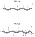
- Fig. 1 is a cross-sectional view showing a piezoelectric vibrator unit 5 according to an embodiment of the present invention.
- the vibrator unit 5 includes an elastically deformable plate 1, made of piezoelectric material, e.g., PZT.
- the plate 1 may be about 7 ⁇ m thick.
- the elastic plate 1 has a surface including troughs or curved portions 2 which are laterally spaced at fixed pitches.
- a common electrode 3 is layered over one side of the elastic plate 1.
- platinum is vapor deposited over one side of the elastic plate 1.
- one side of the elastic plate may be coated with a conductive material which forms the common electrode 3.
- Discrete electrodes 4 are layered on the other side of the elastic plate 1 over the curved portions 2 that serve as deformable regions.
- the discrete electrodes 4 may be formed by vapor depositing platinum or the like over the surfaces of the curved portions 1.
- the surface of the curved portions 2 of the elastic plate 1 may be coated with conductive material which forms the discrete electrodes 4.
- a drive voltage is applied between the common electrodes 3 and at least one of the discrete electrodes 4.
- the deformable region of the elastic plate 1 which is sandwiched between those electrodes 3 and 4 contracts, so that the corresponding curved portion 2 is displaced outwardly (upwardly in the drawing), as shown in Fig. 1(b).
- the length L of the deformable region of the elastic plate 1 is increased to the length L' when the side edges of the deformable region are held by the corresponding side edges of one of the discrete electrodes 4.
- a tension is generated in the deformable region.
- the deformable region varies its curvature. Consequently, the curved portion 2 moves upwards and reduces its depth by ⁇ H.
- the deformable regions of the elastic plate 1 of the single layer structure which are defined by the discrete electrodes, may be selectively deformed when a drive signal is applied between the common electrode 3 and at least one of the discrete electrodes 4 which defines that region.
- a magnitude of deflection of the elastic plate 1 is maximized when a magnitude of deflection ⁇ H of the deformable region of the elastic plate 1 is selected to be one to two times as large as the thickness of the elastic plate 1.
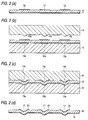
- Figs. 2(a)-2(d) show a sequence of process steps of a method of manufacturing the piezoelectric vibrator unit according to the present invention.
- a common electrode 11 is formed on one side of a green sheet 10 and discrete electrodes 12 are formed on the other side thereof.
- the green sheet 10 is made of piezoelectric material, e.g., PZT.
- the common electrode 11 consists of a deformable layer, made of a conductive material, formed by coating, as shown in Fig. 2a.
- the green sheet 10 is then placed between a lower mold 13 and an upper mold 14, as shown in Fig. 2(b).
- the discrete electrodes 12 on the green sheet 10 are confronted with inwardly curved portions 13a of the lower mold 13, which are configured in conformity with the above-mentioned curved portions.
- the upper mold 14 having outwardly curved portions 14a is positioned so that the outwardly curved portions 14a thereof are confronted with the discrete electrodes 12 of the green sheet 10.
- the green sheet 10 is then pressed between the upper and lower molds 13 and 14 by applying a fixed pressure to the upper mold 14.
- the green sheet 10 and the electrodes 11 and 12 are configured as defined by the shapes of the upper and the lower molds 13 and 14, as shown in Fig. 2(c).
- the green sheet 10 is taken out of the lower and upper molds 13 and 14, or while the green sheet 10 is kept to be placed between the molds 13 and 14 under a fixed pressure, the green sheet 10 is sintered at a temperature, e.g., 1200°C, which is sufficient to transform its nature into a ceramic. In this way, a piezoelectric vibrator unit is manufactured.
- a temperature e.g. 1200°C
- the resulting piezoelectric vibrator unit consists of an elastic plate 18 having curved portions 17 configured as defined by the inwardly and outwardly curved portions 13a and 14a of the molds 13 and 14, a common electrode 19 layered on one side of the elastic plate 18, and drive (i.e., discrete) electrodes 20 formed and discretely arrayed on the other side thereof, as shown in Fig. 2(d).
- the common electrode 19 and the discrete electrodes 20 are attached to the green sheet 18 before the green sheet 18 is subjected to the above process.
- a piezoelectric vibrator unit is also provided in accordance with the present invention, as shown in Figs. 3(a)-3(e).
- the green sheet 10 made of piezoelectric material is molded and sintered in the manner shown in Figs. 3(a)-3(c).
- An elastic plate 18 is then formed which has curved portions 17 that are defined by the inwardly and outwardly curved portions 13a and 14a of the molds 13 and 14, as shown in Fig. 3(d).
- a common electrode 19 is formed on one side of the elastic plate 18, and drive (i.e., discrete) electrodes 20 are formed on the curved portions 17 of the other side of the elastic plate 18, as shown in Fig. 3(e).
- a vapor deposition or sputtering process may be used to form the common and discrete electrodes 19 and 20 on the surfaces of the elastic plate 18.
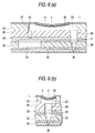
- Figs. 4(a)-4(d) show a method of manufacturing a piezoelectric vibrator unit in accordance with another embodiment the present invention.
- a common electrode 11 is formed on one side of a green sheet 10, and discrete electrodes 12 are formed on the other side thereof.
- the green sheet 10 is made of piezoelectric material, e.g., PZT.
- the common electrode 11 consists of a deformable layer made of conductive material, which maybe formed as a coating, as shown in Fig. 4(a).
- Lumps 15 are then placed on the surfaces of the discrete electrodes 12 at the same pitches as the curved portions 17 (i.e., deformable regions) to be formed, as shown in Fig. 4(a).
- Each of the lumps 15 has a proper shape for forming the curved portions 17 of an elastic plate when the lumps are pressed by an upper mold 14.
- the green sheet 10 is sandwiched between a lower mold 13 and an upper mold 14, as shown in Fig. 4(b).
- the lower mold 13 has inwardly curved portions 13a that are configured in conformity with the shape of the curved portions 17.
- the upper mold 14 has depressions 14b which are deep enough to allow the upper mold to press the lumps 15, as shown in Fig. 4(b).
- the green sheet 10 is compressed by the molds 13 and 14 to which a fixed force is applied.
- the surface of the green sheet 10 on which the discrete electrodes 12 are formed (which corresponds to deformable regions of the green sheet 10) are inwardly deformed due to the presence of the lumps 15.
- portions of the other surface of the green sheet 10 on which the common electrode 11 is formed (which also correspond to the deformable regions of the green sheet 10) are outwardly deformed as defined by the configuration of the inwardly curved portions 13a of the lower mold 13.
- the green sheet 10 is taken out of the molds 13 and 14, or while the green sheet 10 is kept to be placed between the molds 13 and 14 to which a fixed pressure is applied, the green sheet 10 is sintered at a temperature, e.g., 1200°C, which is sufficient to transform the green sheet 10 into a ceramic.
- a temperature e.g. 1200°C
- the lumps 15 are moltened away, as shown in Fig. 4(c). In this manner, the inventive piezoelectric vibrator unit is manufactured.
- the piezoelectric vibrator unit consists of an elastic plate 18 having curved portions 17 which are defined by the inwardly curved portions 13a of the lower mold 13 and the contour of the lumps 15, a common electrode 19 layered on one side of the elastic plate 18, and discrete (i.e., drive) electrodes 20 formed on the curved portions 17 of the other side of the elastic plate, as shown in Fig. 4(d).
- a green sheet 10 is first subjected to the shaping and sintering process using the lumps 15, and the molds 13 and 14. Then, a common electrode 11 and discrete electrodes 12 are disposed on the shaped and sintered green sheet 10.
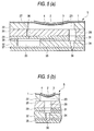
- Figs. 5(a) and 5(b) show a component ink jet recording head utilizing a piezoelectric vibrator unit 5 constructed in accordance with the present invention.
- the ink jet recording head includes a spacer 22 formed from a ceramic plate made of zirconia, for example.
- the spacer 22 has a proper thickness for forming pressure generating chambers 23 (e.g., 150 ⁇ m).
- Through-holes 27 and 28, which are configured so as to conform the pressure generating chambers 23, are formed at fixed pitches in the spacer 22.
- the pressure generating chamber 23 may have a discharge orifice pitch which is 90 dpi, a width which is 190 to 210 ⁇ m, and a length which is about 2mm.
- the inventive piezoelectric vibrator unit 5 serves as a first covering member which covers and seals one of the sides of the spacer 22.
- an initial deflection of each of the curved portions 17 of the piezoelectric vibrator unit is selected to be 5 ⁇ or larger, preferably about 30 ⁇ m or larger at the deepest part thereof, and generally one to two times as large as the thickness of the elastic plate 18.
- a second covering member 26 covers and seals the other side of the spacer 22.
- the second covering member 26 is made of zirconia, for example.
- the piezoelectric vibrator unit 5, the spacer 22, and the second covering member 26 define the pressure generating chamber 23.
- the second covering member includes a first through-hole 27 which communicates with one end of the pressure generating chamber 23, and a second through-hole 28 which communicates with the other end of the pressure generating chamber 23.
- an ink-supply-port forming plate 29 which may be made of zirconia, is fixed to the second covering member 26.
- the ink-supply-port forming plate 29 further includes a through-hole 31 which is formed at a location corresponding to the second through-hole 28 of the second covering member 26.
- An ink-chamber forming plate 32 is formed from a plate member having a proper thickness for forming a common ink chamber by way of example, the plate member may be 150 ⁇ m thick and may be formed of zirconia.
- the ink supply port 30 has an opening at the top of the common ink chamber 33.
- a through-hole 34 which is formed in the ink-chamber forming plate 32, communicatively connects the pressure generating chamber 23 with a discharge orifice 36.
- a nozzle plate 35 is also provided in the ink jet recording head.
- the nozzle plate 35 is a metal plate member, such as stainless steel.
- the metal plate member is corrosion resistant to ink.
- a discharge orifice 36 is formed in the nozzle plate at a location which corresponds to the pressure generating chamber 23 so that it is communicatively connected to the pressure generating chamber 23 via the through-holes 28, 31 and 34.
- the nozzle plate 35 is bonded to the ink-chamber forming plate 32 by means of a bonding layer 37, e.g., a thermally molten film, inserted therebetween.
- a bonding layer 38 is also provided for bonding the ink-supply-port forming plate 29 to the common ink-chamber forming plate 32.
- a drive voltage is applied between the common electrode 3 and a discrete (i.e, drive) electrode 4 which are associated with the pressure generating chamber 23 so that only the region sandwiched between the electrodes 3 and 4, (i.e., the deformable region) contracts.
- the curved portion 2 moves upwards and its bottom rises by an amount ⁇ H, as shown in Fig. 1(b).
- the elastic plate 1 includes curved portions 2 that are formed by curving the elastic plate per se.
- the expansion and/or contraction of the elastic plate 1 can easily vary the volume of the pressure generating chamber, as compared to the case in which a deflection deformation is caused by expanding and contracting a planar vibrating plate. Therefore, the volume of the pressure generating chamber 23 increases when it sucks ink into itself and decreases when it discharges the ink droplet at a faster rate when a curved vibrating plate is used in the ink jet recording head instead of a planar vibrating plate. As a result, ink droplets can be more efficiently discharged from the ink jet recording head under the application of the same drive signal.
- the electrode 3 is used as a common electrode.
- at least one discrete electrode 39 is used in place of the common electrode as shown in Figs. 6(a) and 6(b).
- the electrode 39 is formed on the lower side of the deformable region so that it is exposed to the pressure generating chamber 23.
- Figs. 7(a) and 7(b) show an ink jet recording head incorporating a piezoelectric vibrator unit according to another aspect of the present invention.
- a vibration inducing plate 40 is layered on the common electrode 3 on the inner side of each curved portion 2 of the elastic plate 1.
- the vibration inducing plate 40 extends in the longitudinal direction of the pressure generating chamber 23 and on a central line on the inner side of the curved portion 2.
- the vibration inducing plate 40 is made of a material having a larger rigidity than the piezoelectric material of the elastic plate 1.
- the vibration inducing plate 40 may be made of metal or ceramic.
- a vibration inducing plate may be formed on the discrete electrode alone, or in addition to the vibration inducing plate which is formed on the common electrode.
- the vibration inducing plate 40 cooperates with the elastic plate 1 to provide a bimetal effect. Therefore, the deformable region is more easily bendable, and its endurance against a pressure generated at the time of applying pressure to the ink is improved by an amount corresponding to the increase of the thickness of the deformable region structure. Accordingly, pressure can be efficiently applied to the ink.
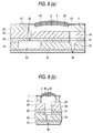
- the curved portions 2 of the elastic plate 1 are each curved toward the pressure generating chamber 23.
- those curved portions 2 may also be outwardly curved, as shown in Figs. 8(a) and 8(b).
- the vibration inducing plates 40 may be formed on the side of the elastic plate 1 that faces the pressure generating chambers 23.
- the common electrodes 3 are exposed to ink in the pressure generating chambers 23. Therefore, the common electrodes 3 are preferably covered with layers (each having a thickness, e.g., 1 ⁇ m) which will not interrupt a vibration of the deformable region structure. These layers may be made of piezoelectric material, such as silicon oxide, zirconia, or the like. Where the electrodes 3 are covered with the layers, the electrodes are separated from ink and prevented from being corroded.
- the spacer 22 and the covering member 26 may be formed from ceramic material other than zirconia, such as alumina. Further, if the spacer 22, the covering member 26 and the elastic plate 1 are made of the same material, those members may be formed in a one-piece construction.
- Fig. 9 shows a piezoelectric vibrator unit according to another embodiment of the present invention.
- the piezoelectric vibrator unit includes thin plates 43 and 44 made of piezoelectric material which are curved so as to form curved portions 45 that are lengthwise arrayed at fixed pitches.
- Individual electrodes 46 are buried in the curved portions 45, as shown in Fig. 9.
- common electrodes 47 and 48 are layered on the exposed surfaces of the thin plates 43 and 44 made of piezoelectric material.
- a drive signal is applied to those electrodes 46, 47 and 48 in order to generate electric fields, which are in the same direction, so that a deformable region of the curved portion 45 is deformed. Since the plates 43 and 44 made of piezoelectric material are thin, a low voltage of the drive signal may be used for generating the required electric fields.
- Fig. 10 is a partial cross-sectional view showing an ink jet recording head incorporating the piezoelectric vibrator unit of Fig. 9. With the exception of the piezoelectric vibrator unit, the ink jet recording head is similar the embodiments described above.
- the piezoelectric vibrator unit is fixed to the spacer 22 so that the curved portion 45 is located in the corresponding pressure generating chamber 23 defined by the spacer 22.
- the ink droplet can be discharged by a relatively low drive voltage.
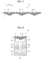
- Fig. 11 is a cross-sectional view showing a piezoelectric vibrator unit 51 according to yet another embodiment of the present invention.
- the piezoelectric vibrator unit 51 includes fillers 50 which are placed on and along the upper side of the curved portions 2 of the piezoelectric vibrator unit 51.
- the piezoelectric vibrator unit 51 may be made of high polymer, for example. In all other respects, the piezoelectric vibrator unit 51 is similar to the one shown in Fig. 1(a).
- Fig. 12 is a partial cross-sectional view showing an ink jet recording head incorporating the piezoelectric vibrator unit 51 of Fig. 11.
- the ink jet recording head is similar to the embodiments described above.
- the piezoelectric vibrator unit 51 is fixed to a spacer 22 so that the lower side of a curved portion 2 thereof is located in a corresponding pressure generating chamber 23 defined by the spacer 22.
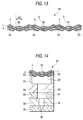
- Fig. 13 is a cross-sectional view showing a piezoelectric vibrator unit according to yet another embodiment of the present invention.
- fillers 52 are disposed on the upper side of the curved portions 2 of the elastic plate 1.
- the width w2 of each filler 52 is slightly shorter than the width w1 of the filler 50 shown in the Fig. 11.
- second fillers 53 are placed on a lower side of the curved portions 2 of the elastic plate 1.
- Each of the second fillers 53 extends so that its left end reaches a position corresponding to the right end of an adjacent filler 52 located to the left of that filler 53.
- the right end of each filler 53 reaches to a position corresponding to the left end of an adjacent filler 52 located on the right side of that filler 53.
- Fig. 14 is a partial cross-sectional view showing an ink jet recording head incorporating the piezoelectric vibrator unit of Fig. 13.
- the piezoelectric vibrator unit 54 is similar to the embodiments described above.
- the piezoelectric vibrator unit 54 is fixed to a spacer 22 so that the lower side of a curved portion 2 is located in a corresponding pressure generating chamber 23 defined by the spacer 22.
- Portions of the second fillers 53 are put on corresponding surfaces of walls of the pressure generating chamber 23, the walls being defined by the spacer 22.
- Fig. 15 is a cross-sectional view showing a piezoelectric vibrator unit according to yet another embodiment of the present invention.
- the piezoelectric vibrator unit 56 includes a filler 55 which is placed on the upper side of each curved portion 2 of an elastic plate 1.
- the filler 55 may be configured independently of the shape of the curved portion 2.
- Fig. 16 is a partial cross-sectional view showing an ink jet recording head incorporating the piezoelectric vibrator unit 56 of Fig. 15.
- the ink jet recording head is similar to the embodiments described above.
- the piezoelectric vibrator unit 56 is fixed to the spacer 22 so that the lower side of a curved portion 2 is located in a corresponding pressure generating chamber 23 defined by the spacer 22.
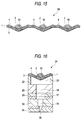
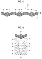
- Fig. 17 is a cross-sectional view showing a piezoelectric vibrator unit according to still yet another embodiment of the present invention.
- an elastic plate is formed from a couple of layered thin plates 58 and 59.
- discrete electrodes 57 are sandwiched between the thin plates 58 and 59 at the locations of corresponding curved portions 2.
- Common electrodes 60 and 61 are layered on the upper and lower sides (when viewed in the drawing) of the elastic plate.
- fillers 62 which are upwardly curved, are placed on the upper side of the curved portions 2.
- Fig. 18 is a partial cross-sectional view showing an ink jet recording head incorporating the piezoelectric vibrator unit 63 of Fig. 17.
- the ink jet recording head is similar to the embodiments described above.
- the piezoelectric vibrator unit 63 is fixed to a spacer 22 so that a lower side of a curved portion 2 is located in a corresponding pressure generating chamber 23 defined by the spacer 22.
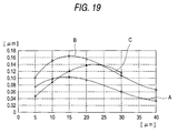
- Fig. 19 is a graph showing variations A, B and C of the magnitude of deflection of the curved portions of the piezoelectric vibrator units shown in Figs. 9, 11 and 13, respectively, with respect to an initial deflection magnitude thereof.
- the magnitude of deflection of each of the curved portions was measured under a fixed voltage of a drive signal that is applied to the curved portion of the piezoelectric vibrator unit.
- the thickness of the elastic plate used was 10 ⁇ m.
- the curved portions of the elastic plate were arrayed at pitches of 150 ⁇ m along the piezoelectric vibrator unit.
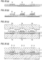
- Figs. 20(a)-20(d) shows an embodiment of a method of manufacturing a piezoelectric vibrator unit which is similar to the one shown in Fig. 2(d).
- discrete electrodes 12 are formed on one side of a green sheet 10 in the regions thereof which will define the inwardly curved side of the curved portions of the piezoelectric vibrator unit, as shown in Fig. 20(a).
- the discrete electrodes 12 are deformable and are made of conductive material.
- the electrodes 12 may be formed as a conductive coating.
- the green sheet 10 is made of piezoelectric material, such as PZT. If necessary, a common electrode 11 can be provided which is also deformable and made of conductive material.
- the common electrode 11 is formed on the other side of the green sheet 10, as shown in Fig. 20(b).
- green sheets 70 which are used as fillers, are formed on the discrete electrodes 12.
- the green sheets 70 are made of heat resistant material, e.g., ceramic, which is deformable when it is under pressure.
- the green sheet 10 having the electrodes 11 and 12 and the green sheets 70 is inserted between a lower mold 13 and an upper mold 14, as shown in Fig. 20(c).
- the lower mold 13 has inwardly curved portions 13a which are each configured in conformity with a curved portion of the piezoelectric vibrator unit.
- the upper mold 14 has outwardly curved portions 14a. Subsequently, the green sheet 10 is compressed with the upper and lower molds 14 and 13 so that the green sheet 10, having the electrodes and the green sheets 70, is molded into a shape defined by the combined molds 13 and 14, as shown in Fig. 20(d).
- the green sheet 10 is taken out of the molds 13 and 14, or while the green sheet 10 is kept to be placed between the molds 13 and 14 under a fixed pressure, the green sheet 10 is sintered at a temperature, e.g., 1200°C, which is sufficient to transform it into a ceramic.
- a temperature e.g. 1200°C
- the green sheet 10 made of piezoelectric material, and the green sheets 70, which will be used as fillers, are transformed into a ceramic so that a piezoelectric vibrator unit is manufactured.
- the green sheet 10 is sintered after the common electrode 11 is formed thereon.
- the common electrode may be formed on the green sheet 10 by vapor deposition, sputtering, or the like after the green sheet is sintered.
- the fillers are formed by a sintering process, they also may be formed so that the curved portions 2 of the piezoelectric vibrator unit 5 are coated with a high polymer.
- the electrodes are provided on both sides of the elastic plate.
- the piezoelectric vibrator unit is incorporated into the recording head, the common electrode formed on the reverse side of the elastic plate is covered with the spacer of the recording head. Therefore, it is difficult to connect the electrode to an external drive circuit.
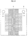
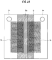
- a conductive layer 72 is formed on the surface of the spacer 22 to which piezoelectric vibrator units will be fixed.
- the conductive layer 72 extends through a region of the spacer surface which contacts the common electrodes 75 of the piezoelectric vibrator unit 74 and a region of the spacer surface, which is free from a vibration of the piezoelectric vibrator units 74 (the central region of the spacer surface where two series of pressure generating chambers 23 are confronted with each other in this embodiment).
- the piezoelectric vibrator units 74 are set on the spacer 22 with the conductive layer 72 such that the curved portions 2 of the piezoelectric vibrator units 74 are positioned within the pressure generating chambers 23, as shown in Fig. 23, the piezoelectric vibrator units 74 are formed having corresponding widths, W3 and W3'. These dimensions ensure that a gap 73 is produced between the vibrator units 74.
- the common electrode 75 is formed to reach the conductive layer 72 of the spacer 22 so that the later has an exposed portion 72a, as shown in Fig. 23.
- the exposed portion 72a of the conductive layer 72 is connected to an external drive circuit by a flexible cable, for example.
- two piezoelectric vibrator units are separately arranged.
- a single piezoelectric vibrator unit may be applied to the two series of pressure generating chambers of the spacer, as a matter of course.
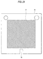
- a piezoelectric vibrator unit 76 is cut out to form a cutout portion 78 which faces a conductive layer 77 of the spacer 22.
- the cutout portion 78 the conductive layer 77 formed on the spacer may be exposed through the cutout portion 78 even when the piezoelectric vibrator unit is layered over the spacer.
- the piezoelectric vibrator unit is sintered, and then fixed to the spacer 22 in the above-mentioned embodiments depicted in Figs. 21-24.
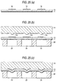
- the spacer 22 may be used for a molding member in order to form the deflecting member of the piezoelectric vibrator unit of the present invention. The use of the spacer in this fashion is shown in Figs. 25(a)-(c).
- a common electrode 11 may be formed on one side of a green sheet 10 and discrete electrodes 12 formed on the other side thereof, as shown in Fig, 25(a).
- the green sheet 10 is made of piezoelectric material, for example, PZT.
- the common electrode 11 is deformable and made of conductive material, such as a conductive coating.
- the green sheet 10 having the electrodes 11 and 12 is positioned so that the discrete electrodes 12 on the green sheet 10 lie above the pressure generating chambers 23 of the spacer 22, respectively.
- An upper mold 14 is provided which has outwardly curved portions 14a arrayed at the same pitches as the pressure generating chambers 23, as shown in Fig. 25(b).
- the spacer 22 is used as a lower mold.
- the upper mold 14 is pressed against the green sheet 10 and the lower mold 22 by applying a fixed pressure to the upper mold 14, as shown in Fig. 25(c).
- the green sheet 10 and the electrodes 11 and 12 are configured as defined by the shape of the outward curved portions 14a of the upper mold 14.
- the green sheet 10 is then sintered at a temperature, e.g., 1200°C, which is sufficient to transform it into a ceramic.
- a temperature e.g. 1200°C
- the piezoelectric vibrator unit is bonded to the spacer 22 by the process of sintering, without using adhesive.
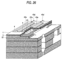
- Figs. 26, 27(a) and 27(b) show an ink jet recording head in which a piezolectric vibrator unit in accordance with another embodiment of the present invention is used.
- no curved portions are formed in the elastically deformable plate.
- first and second vibration inducing plates 40a and 40b are layered on the electrode 3 and 4.
- the first vibration inducing plates 40a are formed on the surface of the discrete electrodes 4 and the second vibration inducing plates 40b are formed on the surface of the common electrode 3.
- a lead-out electrode 40a' which is continuous to the first vibration inducing plates 40a, is extended to beyond the pressure generating chamber 23.
- a common electrode 4 is formed, by sputtering or vapor deposition, in a region of one of the major surfaces of a green sheet made of piezoelectric material, e.g., PZT, which will be formed into a vibrating plate by sintering, the region facing the pressure generating chambers 23.
- second vibration inducing plates 40b are formed on the surface of the common electrode 4 such that a gap is created in a region facing the pressure generating chambers 23, and the second vibration inducing plates 40b are respectively centered at the partitioning walls 22a of the spacer 22 partitioning the pressure generating chamber 23.
- thick-film plating, sputtering, a thick-film printing method, or the like may be used for forming the second vibration inducing plates 40b.
- the structure formed in the above-mentioned process is bonded to one of the major surfaces of the spacer 22, and the covering member 26 is bonded to the other major surface of the spacer 22.
- the discrete electrodes 4 and the first vibration inducing plates 40a are not yet formed on the surface of the elastic plate 1. Therefore, it never happens that the elastic plate 1 subsides into the pressure generating chambers 23 and is deflected. Accordingly, pressure is applied to the elastic plate 1 uniformly over its entire surface, and the respective layers are reliably bonded together.
- the structure is sintered to complete a semi-product of a piezolectric vibrator unit not having the discrete electrodes 4 and the first vibration inducing plates 40a which will be famed on the upper surface of the elastic plate 1. Then, discrete electrodes 4 are formed on the surface of the semi-product 50 as to face the pressure generating chambers 23 by sputtering or vapor depositing conductive material. Metal is vapor deposited over the surface of the structure, and first vibration inducing plates 40a of ceramic are formed thereon by a thick-film printing method.
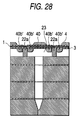
- Figs. 28 shows an ink jet recording head in which a piezolectric vibrator unit similar to the embodiment in Figs. 27(a) and 27(b) is used.
- the second vibration inducing plate 40b is formed of a continuous body put on the related partitioning wall 22a of the spacer 22.
- the second vibration inducing plate 40b has two separate bodies 40b' and 40b'.
Abstract
Description
- The present invention relates to a piezoelectric vibrator unit, an ink jet recording head using the piezoelectric vibrator unit, a method of manufacturing a piezoelectric vibrator unit and a method of manufacturing an ink jet recording head. In particular, the present invention relates to a piezoelectric vibrator unit suitable for an ink jet recording head and having curved portions which correspond to deformable regions of the vibrator unit.
- An actuator unit in which minute regions (arrayed at fixed pitches) are deflected is disclosed in Japanese Patent Laid-Open Publication No. Sho. 58-7364. The actuator unit includes a lower electrode, formed on the surface of a thin plate, which is elastically deformable. A green sheet, which is shaped like a rectangular strip and made of piezoelectric material, is layered on the thin plate surface with the lower electrode by bonding or coating. The resultant structure is sintered to form a piezoelectric layer. In addition, upper electrodes are formed on the surface of the sintered structure.
- However, the bonding or coating process, by which the rectangular green sheet made of piezoelectric material is layered on the thin plate's surface is an essential step in the manufacture of the above-mentioned actuator unit. Therefore, the manufacturing of the actuator unit is inefficient. Furthermore, the lower electrode is easily peeled away from the piezoelectric layer in the sintering process. In this respect, the actuator unit is poor in durability.
- To cope with this, a unique actuator unit is proposed in Japanese Patent Laid-Open Publication No. Sho. 62-101455. The actuator unit includes a thin elastic plate made of ceramic which has an electromechanical displacing property. A ceramic piece is inserted in a region of the elastic plate which is to be deflected. In addition, electrodes are attached to both sides of the region containing the ceramic piece.
- The actuator unit described above eliminates the need for the bonding or coating process associated with the green sheet of piezoelectric material. In addition, the piezoelectric member has a single layer structure. Therefore, it rarely happens that the electrode is peeled away. However, the actuator unit has the following disadvantage. An elasticity and a rigidity of a vibrating region of the elastic plate are substantially equal to those in a non-vibrating region. Therefore, a displacement of the vibrated region by its deflection is small. Accordingly, when the actuator unit is applied to an ink jet recording head in which the volume of the pressure generating chamber is varied in order to discharge an ink droplet, a high voltage is required in order to drive the recording head.
- It is therefore the object of the present invention to overcome the above described problems and to provide a piezoelectric vibrator unit having a single layer structure that allows for a greater displacement of the vibrating plate, and an ink jet recording head provided with such a piezoelectric vibrator unit.
- This object is solved by the piezoelectric vibrator unit according to
claim 1, the layered ink jet type recording head according toindependent claims independent claims - According to an advantageous aspect of the invention, the piezoelectric vibrator unit may be manufactured without any bonding or coating process for forming a piezoelectric member.
- According to a further aspect of the present invention, a method of manufacturing the piezoelectric vibrator unit shall be provided. According to another aspect of the present invention, an ink jet recording head using the piezoelectric vibrator unit shall be provided.
- In order to carry out the above object of the invention, a piezoelectric vibrator unit is provided in accordance with a first embodiment of the present invention. The piezoelectric vibrator unit includes an elastically deformable plate made of piezoelectric material having curved portions lengthwise arrayed at fixed pitches. Preferably, a common electrode is formed on one side of the elastic plate, while discrete electrodes are formed on the curved portions of the elastic plate.
- An extension and a contraction of the elastic plate are converted into deflection displacements that are made in conformity with a shape of each curved portion. Advantageously, the piezoelectric vibrator unit may be included in an ink jet recording head in which a pressure generating chamber is included. A rate of change of the volume of the pressure generating chamber per unit drive voltage is increased by employing the above mentioned elastically deformable plate having the curved portions instead of a vibrator unit including a flat plate.
- These and other features, aspects and advantages of the present invention will become better understood with reference to the following description, appended claims, and accompanying drawings, in which:
- Figs. 1(a) and 1(b) are cross-sectional views showing a piezoelectric vibrator unit according to an embodiment of the present invention. Fig. 1(a) is a cross-sectional view showing the piezoelectric vibrator unit when a drive signal is not applied thereto. Fig. 1(b) is a cross-sectional view showing the piezoelectric vibrator unit when a drive signal is applied between one discrete electrode and a common electrode in the vibrator unit.
- Figs. 2(a) to 2(d) are sectional views showing a sequence of process steps of a method of manufacturing a piezoelectric vibrator unit according to another embodiment of the present invention.
- Figs. 3(a) to 3(e) are sectional views showing a sequence of process steps of a method of manufacturing a piezoelectric vibrator unit according to yet another embodiment of the present invention.
- Figs. 4(a) to 4(d) are sectional views showing a sequence of process steps of a method of manufacturing a piezoelectric vibrator unit according to still yet another embodiment the present invention.
- Figs. 5(a) and 5(b) are cross-sectional views showing a portion of an ink jet recording head utilizing a piezoelectric vibrator unit constructed in accordance with the present invention.
- Figs. 6(a) and 6(b) are cross-sectional views showing another ink jet recording head utilizing a piezoelectric vibrator unit constructed in accordance with the present invention.
- Figs. 7(a) and 7(b) are cross-sectional views showing still another ink jet recording head utilizing a piezoelectric vibrator unit constructed in accordance With the present invention.
- Figs. 8(a) and 8(b) are cross-sectional views showing yet another ink jet recording head utilizing a piezoelectric vibrator unit constructed in accordance with the present invention.
- Fig. 9 is a cross-sectional view showing still yet another embodiment of a piezoelectric vibrator unit according to the present invention.
- Fig. 10 is a partial cross-sectional view showing an ink jet recording head incorporating the piezoelectric vibrator unit of Fig. 9.
- Fig. 11 is a cross-sectional view showing a piezoelectric vibrator unit according to another embodiment of the present invention.
- Fig. 12 is a partial cross-sectional view showing an ink jet recording head incorporating the piezoelectric vibrator unit of Fig. 11.
- Fig. 13 is a cross-sectional view showing a piezoelectric vibrator unit according to yet another embodiment of the present invention.
- Fig. 14 is a partial cross-sectional view showing an ink jet recording head incorporating the piezoelectric vibrator unit of Fig. 13.
- Fig. 15 is a cross-sectional view showing a piezoelectric vibrator unit according to still yet another embodiment of the present invention.
- Fig. 16 is a partial cross-sectional view showing an ink jet recording head incorporating the piezoelectric vibrator unit of Fig. 15.
- Fig. 17 is a cross-sectional view showing a piezoelectric vibrator unit according to still another embodiment of the present invention.
- Fig. 18 is a partial cross-sectional view showing an ink jet recording head incorporating the piezoelectric vibrator unit of Fig. 17.
- Fig. 19 is a graph showing variations of the quantities of deflection of the curved portions of the piezoelectric vibrator units of Figs. 9, 11 and 13 with respect to initial deflection quantities thereof.
- Figs. 20(a) to 20(d) are sectional views showing a sequence of process steps of an additional embodiment of a method of manufacturing a piezoelectric vibrator unit according to the present invention.
- Fig. 21 is a diagram showing a structure for leading out an electrode formed on a piezoelectric vibrator unit in an ink jet recording head using the piezoelectric vibrator unit as an actuator.
- Fig. 22 is a diagram showing the rear sides of the separated piezoelectric vibrator units in the electrode lead-out structure of Fig. 21.
- Fig. 23 is a diagram showing a conductive layer formed on the spacer and common electrodes formed on the rear sides of the piezoelectric vibrator units in the electrode lead-out structure of Fig. 21.
- Fig. 24 is a diagram showing another electrode lead-out structure in an ink jet recording head using the piezoelectric vibrator unit as an actuator.
- Figs. 25(a) to 25(c) are sectional views showing a sequence of process steps of a method of manufacturing a piezoelectric vibrator unit according to an embodiment of the present invention.
- Fig. 26 is a perspective view showing a piezoelectric vibrator unit according to another embodiment of the present invention.
- Fig. 27(a) is a lengthwise cross sectional view of the recording head in Fig. 26. Fig. 27(b) is a widthwise cross sectional view of the recording head in Fig. 26.
- Fig. 28 is a cross sectional view of a piezoelectric vibrator unit according to another embodiment of the present invention.
- The preferred embodiments of the present invention, which are illustrated in detail in the accompanying drawings, will be described hereunder.
- Fig. 1 is a cross-sectional view showing a
piezoelectric vibrator unit 5 according to an embodiment of the present invention. Thevibrator unit 5 includes an elasticallydeformable plate 1, made of piezoelectric material, e.g., PZT. By way of example, theplate 1 may be about 7µm thick. Theelastic plate 1 has a surface including troughs orcurved portions 2 which are laterally spaced at fixed pitches. Acommon electrode 3 is layered over one side of theelastic plate 1. - To form the
common electrode 3, platinum is vapor deposited over one side of theelastic plate 1. Alternatively, one side of the elastic plate may be coated with a conductive material which forms thecommon electrode 3.Discrete electrodes 4 are layered on the other side of theelastic plate 1 over thecurved portions 2 that serve as deformable regions. Thediscrete electrodes 4 may be formed by vapor depositing platinum or the like over the surfaces of thecurved portions 1. Alternatively, the surface of thecurved portions 2 of theelastic plate 1 may be coated with conductive material which forms thediscrete electrodes 4. - In the above-mentioned embodiment, a drive voltage is applied between the
common electrodes 3 and at least one of thediscrete electrodes 4. Thus, only the deformable region of theelastic plate 1, which is sandwiched between thoseelectrodes curved portion 2 is displaced outwardly (upwardly in the drawing), as shown in Fig. 1(b). Specifically, the length L of the deformable region of theelastic plate 1 is increased to the length L' when the side edges of the deformable region are held by the corresponding side edges of one of thediscrete electrodes 4. As a result, a tension is generated in the deformable region. To balance the tension, the deformable region varies its curvature. Consequently, thecurved portion 2 moves upwards and reduces its depth by ΔH. - In this state, an electric charge of the deformable region defined by the
electrodes elastic plate 1 of the single layer structure, which are defined by the discrete electrodes, may be selectively deformed when a drive signal is applied between thecommon electrode 3 and at least one of thediscrete electrodes 4 which defines that region. - In the above-mentioned piezoelectric vibrator unit, a magnitude of deflection of the
elastic plate 1 is maximized when a magnitude of deflection ΔH of the deformable region of theelastic plate 1 is selected to be one to two times as large as the thickness of theelastic plate 1. - Figs. 2(a)-2(d) show a sequence of process steps of a method of manufacturing the piezoelectric vibrator unit according to the present invention. A
common electrode 11 is formed on one side of agreen sheet 10 anddiscrete electrodes 12 are formed on the other side thereof. Thegreen sheet 10 is made of piezoelectric material, e.g., PZT. Thecommon electrode 11 consists of a deformable layer, made of a conductive material, formed by coating, as shown in Fig. 2a. - The
green sheet 10 is then placed between alower mold 13 and anupper mold 14, as shown in Fig. 2(b). In this case, thediscrete electrodes 12 on thegreen sheet 10 are confronted with inwardlycurved portions 13a of thelower mold 13, which are configured in conformity with the above-mentioned curved portions. Theupper mold 14 having outwardlycurved portions 14a is positioned so that the outwardlycurved portions 14a thereof are confronted with thediscrete electrodes 12 of thegreen sheet 10. Thegreen sheet 10 is then pressed between the upper andlower molds upper mold 14. As a result, thegreen sheet 10 and theelectrodes lower molds - After the
green sheet 10 is taken out of the lower andupper molds green sheet 10 is kept to be placed between themolds green sheet 10 is sintered at a temperature, e.g., 1200°C, which is sufficient to transform its nature into a ceramic. In this way, a piezoelectric vibrator unit is manufactured. - The resulting piezoelectric vibrator unit consists of an
elastic plate 18 havingcurved portions 17 configured as defined by the inwardly and outwardlycurved portions molds common electrode 19 layered on one side of theelastic plate 18, and drive (i.e., discrete)electrodes 20 formed and discretely arrayed on the other side thereof, as shown in Fig. 2(d). - In the manufacturing process mentioned above, the
common electrode 19 and thediscrete electrodes 20 are attached to thegreen sheet 18 before thegreen sheet 18 is subjected to the above process. - Another process for manufacturing a piezoelectric vibrator unit is also provided in accordance with the present invention, as shown in Figs. 3(a)-3(e). According to the inventive manufacturing process, the
green sheet 10 made of piezoelectric material is molded and sintered in the manner shown in Figs. 3(a)-3(c). Anelastic plate 18 is then formed which hascurved portions 17 that are defined by the inwardly and outwardlycurved portions molds - Subsequently, a
common electrode 19 is formed on one side of theelastic plate 18, and drive (i.e., discrete)electrodes 20 are formed on thecurved portions 17 of the other side of theelastic plate 18, as shown in Fig. 3(e). A vapor deposition or sputtering process may be used to form the common anddiscrete electrodes elastic plate 18. - Figs. 4(a)-4(d) show a method of manufacturing a piezoelectric vibrator unit in accordance with another embodiment the present invention. According to the inventive method, a
common electrode 11 is formed on one side of agreen sheet 10, anddiscrete electrodes 12 are formed on the other side thereof. Thegreen sheet 10 is made of piezoelectric material, e.g., PZT. Thecommon electrode 11 consists of a deformable layer made of conductive material, which maybe formed as a coating, as shown in Fig. 4(a).Lumps 15 are then placed on the surfaces of thediscrete electrodes 12 at the same pitches as the curved portions 17 (i.e., deformable regions) to be formed, as shown in Fig. 4(a). Each of thelumps 15 has a proper shape for forming thecurved portions 17 of an elastic plate when the lumps are pressed by anupper mold 14. - The
green sheet 10 is sandwiched between alower mold 13 and anupper mold 14, as shown in Fig. 4(b). Thelower mold 13 has inwardlycurved portions 13a that are configured in conformity with the shape of thecurved portions 17. Theupper mold 14 hasdepressions 14b which are deep enough to allow the upper mold to press thelumps 15, as shown in Fig. 4(b). Thegreen sheet 10 is compressed by themolds green sheet 10 on which thediscrete electrodes 12 are formed (which corresponds to deformable regions of the green sheet 10) are inwardly deformed due to the presence of thelumps 15. In addition, portions of the other surface of thegreen sheet 10 on which thecommon electrode 11 is formed (which also correspond to the deformable regions of the green sheet 10) are outwardly deformed as defined by the configuration of the inwardlycurved portions 13a of thelower mold 13. - After the
green sheet 10 is taken out of themolds green sheet 10 is kept to be placed between themolds green sheet 10 is sintered at a temperature, e.g., 1200°C, which is sufficient to transform thegreen sheet 10 into a ceramic. Through the sintering process, thelumps 15 are moltened away, as shown in Fig. 4(c). In this manner, the inventive piezoelectric vibrator unit is manufactured. - The piezoelectric vibrator unit consists of an
elastic plate 18 havingcurved portions 17 which are defined by the inwardlycurved portions 13a of thelower mold 13 and the contour of thelumps 15, acommon electrode 19 layered on one side of theelastic plate 18, and discrete (i.e., drive)electrodes 20 formed on thecurved portions 17 of the other side of the elastic plate, as shown in Fig. 4(d). - The manufacturing process described above may be modified in the same manner that the first embodiment was modified. According to the modified process, a
green sheet 10 is first subjected to the shaping and sintering process using thelumps 15, and themolds common electrode 11 anddiscrete electrodes 12 are disposed on the shaped and sinteredgreen sheet 10. - Figs. 5(a) and 5(b) show a component ink jet recording head utilizing a
piezoelectric vibrator unit 5 constructed in accordance with the present invention. The ink jet recording head includes aspacer 22 formed from a ceramic plate made of zirconia, for example. Thespacer 22 has a proper thickness for forming pressure generating chambers 23 (e.g., 150µm). Through-holes pressure generating chambers 23, are formed at fixed pitches in thespacer 22. By way of example, thepressure generating chamber 23 may have a discharge orifice pitch which is 90 dpi, a width which is 190 to 210µm, and a length which is about 2mm. - The inventive
piezoelectric vibrator unit 5 serves as a first covering member which covers and seals one of the sides of thespacer 22. To this end, an initial deflection of each of thecurved portions 17 of the piezoelectric vibrator unit is selected to be 5µ or larger, preferably about 30µm or larger at the deepest part thereof, and generally one to two times as large as the thickness of theelastic plate 18. - A
second covering member 26 covers and seals the other side of thespacer 22. Thesecond covering member 26 is made of zirconia, for example. Thepiezoelectric vibrator unit 5, thespacer 22, and thesecond covering member 26 define thepressure generating chamber 23. The second covering member includes a first through-hole 27 which communicates with one end of thepressure generating chamber 23, and a second through-hole 28 which communicates with the other end of thepressure generating chamber 23. - One side of an ink-supply-
port forming plate 29, which may be made of zirconia, is fixed to thesecond covering member 26. Anink supply port 30, which communicates with the first through-hole 27 of thesecond covering member 26, is formed in the ink-supply-port forming plate 29. The ink-supply-port forming plate 29 further includes a through-hole 31 which is formed at a location corresponding to the second through-hole 28 of thesecond covering member 26. - An ink-
chamber forming plate 32 is formed from a plate member having a proper thickness for forming a common ink chamber by way of example, the plate member may be 150µm thick and may be formed of zirconia. Theink supply port 30 has an opening at the top of thecommon ink chamber 33. A through-hole 34, which is formed in the ink-chamber forming plate 32, communicatively connects thepressure generating chamber 23 with adischarge orifice 36. - A
nozzle plate 35 is also provided in the ink jet recording head. Thenozzle plate 35 is a metal plate member, such as stainless steel. Advantageously, the metal plate member is corrosion resistant to ink. Adischarge orifice 36 is formed in the nozzle plate at a location which corresponds to thepressure generating chamber 23 so that it is communicatively connected to thepressure generating chamber 23 via the through-holes nozzle plate 35 is bonded to the ink-chamber forming plate 32 by means of abonding layer 37, e.g., a thermally molten film, inserted therebetween. In addition, abonding layer 38 is also provided for bonding the ink-supply-port forming plate 29 to the common ink-chamber forming plate 32. - In the above-described embodiment, a drive voltage is applied between the
common electrode 3 and a discrete (i.e, drive)electrode 4 which are associated with thepressure generating chamber 23 so that only the region sandwiched between theelectrodes curved portion 2 moves upwards and its bottom rises by an amount ΔH, as shown in Fig. 1(b). - When the
curved portion 2 moves upwards, the volume of thepressure generating chamber 23 increases and ink flows from thecommon ink chamber 33 into thepressure generating chamber 23 through the passage including theink supply port 30 and the first through-hole 27. - In this state, an electric charge of the
elastic plate 1 in the deformable region is discharged and theelastic plate 1 is restored to its original shape. In particular, the original shape of thecurved portion 2 is restored and the volume of thepressure generating chamber 23 decreases. Consequently, thepressure generating chamber 23 compresses ink therein, so chat the ink is discharged outside through thedischarge orifice 36 in the form of an ink droplet. - It is noted that the
elastic plate 1 includescurved portions 2 that are formed by curving the elastic plate per se. With this unique elastic plate, the expansion and/or contraction of theelastic plate 1 can easily vary the volume of the pressure generating chamber, as compared to the case in which a deflection deformation is caused by expanding and contracting a planar vibrating plate. Therefore, the volume of thepressure generating chamber 23 increases when it sucks ink into itself and decreases when it discharges the ink droplet at a faster rate when a curved vibrating plate is used in the ink jet recording head instead of a planar vibrating plate. As a result, ink droplets can be more efficiently discharged from the ink jet recording head under the application of the same drive signal. - In the above-mentioned embodiment, the
electrode 3 is used as a common electrode. In an ink jet recording head which embodies another aspect of the present invention, at least onediscrete electrode 39 is used in place of the common electrode as shown in Figs. 6(a) and 6(b). Theelectrode 39 is formed on the lower side of the deformable region so that it is exposed to thepressure generating chamber 23. - Figs. 7(a) and 7(b) show an ink jet recording head incorporating a piezoelectric vibrator unit according to another aspect of the present invention. As shown in Figs. 7(a) and 7(b), a
vibration inducing plate 40 is layered on thecommon electrode 3 on the inner side of eachcurved portion 2 of theelastic plate 1. In addition, thevibration inducing plate 40 extends in the longitudinal direction of thepressure generating chamber 23 and on a central line on the inner side of thecurved portion 2. Thevibration inducing plate 40 is made of a material having a larger rigidity than the piezoelectric material of theelastic plate 1. By way of example, thevibration inducing plate 40 may be made of metal or ceramic. In addition, a vibration inducing plate may be formed on the discrete electrode alone, or in addition to the vibration inducing plate which is formed on the common electrode. - Advantageously, the
vibration inducing plate 40 cooperates with theelastic plate 1 to provide a bimetal effect. Therefore, the deformable region is more easily bendable, and its endurance against a pressure generated at the time of applying pressure to the ink is improved by an amount corresponding to the increase of the thickness of the deformable region structure. Accordingly, pressure can be efficiently applied to the ink. - In the embodiments mentioned above, the
curved portions 2 of theelastic plate 1 are each curved toward thepressure generating chamber 23. However, thosecurved portions 2 may also be outwardly curved, as shown in Figs. 8(a) and 8(b). In this case, if thevibration inducing plates 40 are required, they may be formed on the side of theelastic plate 1 that faces thepressure generating chambers 23. - In the embodiments mentioned above, the
common electrodes 3 are exposed to ink in thepressure generating chambers 23. Therefore, thecommon electrodes 3 are preferably covered with layers (each having a thickness, e.g., 1µm) which will not interrupt a vibration of the deformable region structure. These layers may be made of piezoelectric material, such as silicon oxide, zirconia, or the like. Where theelectrodes 3 are covered with the layers, the electrodes are separated from ink and prevented from being corroded. - As a further refinement, the
spacer 22 and the coveringmember 26 may be formed from ceramic material other than zirconia, such as alumina. Further, if thespacer 22, the coveringmember 26 and theelastic plate 1 are made of the same material, those members may be formed in a one-piece construction. - Fig. 9 shows a piezoelectric vibrator unit according to another embodiment of the present invention. The piezoelectric vibrator unit includes
thin plates curved portions 45 that are lengthwise arrayed at fixed pitches.Individual electrodes 46 are buried in thecurved portions 45, as shown in Fig. 9. In addition,common electrodes thin plates - In operation, a drive signal is applied to those
electrodes curved portion 45 is deformed. Since theplates - Fig. 10 is a partial cross-sectional view showing an ink jet recording head incorporating the piezoelectric vibrator unit of Fig. 9. With the exception of the piezoelectric vibrator unit, the ink jet recording head is similar the embodiments described above.
- The piezoelectric vibrator unit is fixed to the
spacer 22 so that thecurved portion 45 is located in the correspondingpressure generating chamber 23 defined by thespacer 22. Advantageously, the ink droplet can be discharged by a relatively low drive voltage. - Fig. 11 is a cross-sectional view showing a
piezoelectric vibrator unit 51 according to yet another embodiment of the present invention. Thepiezoelectric vibrator unit 51 includesfillers 50 which are placed on and along the upper side of thecurved portions 2 of thepiezoelectric vibrator unit 51. Thepiezoelectric vibrator unit 51 may be made of high polymer, for example. In all other respects, thepiezoelectric vibrator unit 51 is similar to the one shown in Fig. 1(a). - Fig. 12 is a partial cross-sectional view showing an ink jet recording head incorporating the
piezoelectric vibrator unit 51 of Fig. 11. With the exception of thepiezoelectric vibrator unit 51, the ink jet recording head is similar to the embodiments described above. In the ink jet recording head, thepiezoelectric vibrator unit 51 is fixed to aspacer 22 so that the lower side of acurved portion 2 thereof is located in a correspondingpressure generating chamber 23 defined by thespacer 22. - Fig. 13 is a cross-sectional view showing a piezoelectric vibrator unit according to yet another embodiment of the present invention. In the
piezoelectric vibrator unit 54,fillers 52 are disposed on the upper side of thecurved portions 2 of theelastic plate 1. The width w2 of eachfiller 52 is slightly shorter than the width w1 of thefiller 50 shown in the Fig. 11. In addition,second fillers 53 are placed on a lower side of thecurved portions 2 of theelastic plate 1. Each of thesecond fillers 53 extends so that its left end reaches a position corresponding to the right end of anadjacent filler 52 located to the left of thatfiller 53. Similarly, the right end of eachfiller 53 reaches to a position corresponding to the left end of anadjacent filler 52 located on the right side of thatfiller 53. - Fig. 14 is a partial cross-sectional view showing an ink jet recording head incorporating the piezoelectric vibrator unit of Fig. 13. With the exception of the
piezoelectric vibrator unit 54, the ink jet recording head is similar to the embodiments described above. In the ink jet recording head, thepiezoelectric vibrator unit 54 is fixed to aspacer 22 so that the lower side of acurved portion 2 is located in a correspondingpressure generating chamber 23 defined by thespacer 22. Portions of thesecond fillers 53 are put on corresponding surfaces of walls of thepressure generating chamber 23, the walls being defined by thespacer 22. - Fig. 15 is a cross-sectional view showing a piezoelectric vibrator unit according to yet another embodiment of the present invention. The
piezoelectric vibrator unit 56 includes afiller 55 which is placed on the upper side of eachcurved portion 2 of anelastic plate 1. Thefiller 55 may be configured independently of the shape of thecurved portion 2. - Fig. 16 is a partial cross-sectional view showing an ink jet recording head incorporating the
piezoelectric vibrator unit 56 of Fig. 15. With the exception of thepiezoelectric vibrator unit 56, the ink jet recording head is similar to the embodiments described above. In the ink jet recording head, thepiezoelectric vibrator unit 56 is fixed to thespacer 22 so that the lower side of acurved portion 2 is located in a correspondingpressure generating chamber 23 defined by thespacer 22. - Fig. 17 is a cross-sectional view showing a piezoelectric vibrator unit according to still yet another embodiment of the present invention. In the
piezoelectric vibrator unit 63 of this embodiment, an elastic plate is formed from a couple of layeredthin plates discrete electrodes 57 are sandwiched between thethin plates curved portions 2.Common electrodes fillers 62, which are upwardly curved, are placed on the upper side of thecurved portions 2. - Fig. 18 is a partial cross-sectional view showing an ink jet recording head incorporating the
piezoelectric vibrator unit 63 of Fig. 17. With the exception of thepiezoelectric vibrator unit 63, the ink jet recording head is similar to the embodiments described above. In the ink jet recording head, thepiezoelectric vibrator unit 63 is fixed to aspacer 22 so that a lower side of acurved portion 2 is located in a correspondingpressure generating chamber 23 defined by thespacer 22. - Fig. 19 is a graph showing variations A, B and C of the magnitude of deflection of the curved portions of the piezoelectric vibrator units shown in Figs. 9, 11 and 13, respectively, with respect to an initial deflection magnitude thereof. To plot the graph, the magnitude of deflection of each of the curved portions was measured under a fixed voltage of a drive signal that is applied to the curved portion of the piezoelectric vibrator unit. The thickness of the elastic plate used was 10µm. The curved portions of the elastic plate were arrayed at pitches of 150 µm along the piezoelectric vibrator unit.
- As seen from the graph, in the piezoelectric vibrator unit of Fig. 11 where
fillers 50 are respectively placed on and along (after the shape of) the upper side of thecurved portions 2, a great displacement of the curved portion is caused with its initial deflection being small. - Figs. 20(a)-20(d) shows an embodiment of a method of manufacturing a piezoelectric vibrator unit which is similar to the one shown in Fig. 2(d). Initially,
discrete electrodes 12 are formed on one side of agreen sheet 10 in the regions thereof which will define the inwardly curved side of the curved portions of the piezoelectric vibrator unit, as shown in Fig. 20(a). Thediscrete electrodes 12 are deformable and are made of conductive material. By way of example, theelectrodes 12 may be formed as a conductive coating. Thegreen sheet 10 is made of piezoelectric material, such as PZT. If necessary, acommon electrode 11 can be provided which is also deformable and made of conductive material. Thecommon electrode 11 is formed on the other side of thegreen sheet 10, as shown in Fig. 20(b). In addition,green sheets 70, which are used as fillers, are formed on thediscrete electrodes 12. Thegreen sheets 70 are made of heat resistant material, e.g., ceramic, which is deformable when it is under pressure. - The
green sheet 10 having theelectrodes green sheets 70 is inserted between alower mold 13 and anupper mold 14, as shown in Fig. 20(c). Thelower mold 13 has inwardlycurved portions 13a which are each configured in conformity with a curved portion of the piezoelectric vibrator unit. Theupper mold 14 has outwardlycurved portions 14a. Subsequently, thegreen sheet 10 is compressed with the upper andlower molds green sheet 10, having the electrodes and thegreen sheets 70, is molded into a shape defined by the combinedmolds - After the
green sheet 10 is taken out of themolds green sheet 10 is kept to be placed between themolds green sheet 10 is sintered at a temperature, e.g., 1200°C, which is sufficient to transform it into a ceramic. As a result, thegreen sheet 10, made of piezoelectric material, and thegreen sheets 70, which will be used as fillers, are transformed into a ceramic so that a piezoelectric vibrator unit is manufactured. - In the just described embodiment, the
green sheet 10 is sintered after thecommon electrode 11 is formed thereon. However, the common electrode may be formed on thegreen sheet 10 by vapor deposition, sputtering, or the like after the green sheet is sintered. - Although the fillers are formed by a sintering process, they also may be formed so that the
curved portions 2 of thepiezoelectric vibrator unit 5 are coated with a high polymer. - In the
piezoelectric vibrator unit 5, the electrodes are provided on both sides of the elastic plate. When the piezoelectric vibrator unit is incorporated into the recording head, the common electrode formed on the reverse side of the elastic plate is covered with the spacer of the recording head. Therefore, it is difficult to connect the electrode to an external drive circuit. - An example of a spacer which can solve the above-mentioned problem is shown in Fig. 21. According to the present invention, a
conductive layer 72 is formed on the surface of thespacer 22 to which piezoelectric vibrator units will be fixed. Theconductive layer 72 extends through a region of the spacer surface which contacts thecommon electrodes 75 of thepiezoelectric vibrator unit 74 and a region of the spacer surface, which is free from a vibration of the piezoelectric vibrator units 74 (the central region of the spacer surface where two series ofpressure generating chambers 23 are confronted with each other in this embodiment). - When the
piezoelectric vibrator units 74 are set on thespacer 22 with theconductive layer 72 such that thecurved portions 2 of thepiezoelectric vibrator units 74 are positioned within thepressure generating chambers 23, as shown in Fig. 23, thepiezoelectric vibrator units 74 are formed having corresponding widths, W3 and W3'. These dimensions ensure that agap 73 is produced between thevibrator units 74. In addition, thecommon electrode 75 is formed to reach theconductive layer 72 of thespacer 22 so that the later has an exposedportion 72a, as shown in Fig. 23. To connect the common electrodes of the piezoelectric vibrator units, the exposedportion 72a of theconductive layer 72 is connected to an external drive circuit by a flexible cable, for example. - In the embodiment described above, to expose the conductive layer of the spacer, two piezoelectric vibrator units are separately arranged. However, a single piezoelectric vibrator unit may be applied to the two series of pressure generating chambers of the spacer, as a matter of course. In this case, which is shown in rig. 24, a
piezoelectric vibrator unit 76 is cut out to form acutout portion 78 which faces aconductive layer 77 of thespacer 22. By including thecutout portion 78, theconductive layer 77 formed on the spacer may be exposed through thecutout portion 78 even when the piezoelectric vibrator unit is layered over the spacer. - The piezoelectric vibrator unit is sintered, and then fixed to the
spacer 22 in the above-mentioned embodiments depicted in Figs. 21-24. Advantageously, thespacer 22 may be used for a molding member in order to form the deflecting member of the piezoelectric vibrator unit of the present invention. The use of the spacer in this fashion is shown in Figs. 25(a)-(c). - In particular, a
common electrode 11 may be formed on one side of agreen sheet 10 anddiscrete electrodes 12 formed on the other side thereof, as shown in Fig, 25(a). Thegreen sheet 10 is made of piezoelectric material, for example, PZT. Thecommon electrode 11 is deformable and made of conductive material, such as a conductive coating. - The
green sheet 10 having theelectrodes discrete electrodes 12 on thegreen sheet 10 lie above thepressure generating chambers 23 of thespacer 22, respectively. Anupper mold 14 is provided which has outwardlycurved portions 14a arrayed at the same pitches as thepressure generating chambers 23, as shown in Fig. 25(b). Thespacer 22 is used as a lower mold. - The
upper mold 14 is pressed against thegreen sheet 10 and thelower mold 22 by applying a fixed pressure to theupper mold 14, as shown in Fig. 25(c). As a result, thegreen sheet 10 and theelectrodes curved portions 14a of theupper mold 14. - After the
upper mold 14 is detached from thegreen sheet 10, or while theupper mold 14 is kept to be pressed, thegreen sheet 10 is then sintered at a temperature, e.g., 1200°C, which is sufficient to transform it into a ceramic. Advantageously, the piezoelectric vibrator unit is bonded to thespacer 22 by the process of sintering, without using adhesive. - A displacement of the vibrating plate, which ensues from the expansion and contraction of the vibrating plate, is easily converted into a deflection displacement which is made in conformity with a shape of the curved portion. Therefore, even if the piezoelectric vibrator unit is applied to an ink jet recording head of high density type in which it is required to reduce the volume of each pressure generating chamber, the vibrating plate can be deflected to such an extent as to discharge an ink droplet whose ink amount is required for the printing, by using a high drive voltage.
- Figs. 26, 27(a) and 27(b) show an ink jet recording head in which a piezolectric vibrator unit in accordance with another embodiment of the present invention is used. In this embodiment, no curved portions are formed in the elastically deformable plate. Further, not only one vibration inducing plate as shown in Figs. 7(a)-8(b), but also first and second
vibration inducing plates electrode vibration inducing plates 40a are formed on the surface of thediscrete electrodes 4 and the secondvibration inducing plates 40b are formed on the surface of thecommon electrode 3. A lead-outelectrode 40a', which is continuous to the firstvibration inducing plates 40a, is extended to beyond thepressure generating chamber 23. - In the recording head thus constructed, a
common electrode 4 is formed, by sputtering or vapor deposition, in a region of one of the major surfaces of a green sheet made of piezoelectric material, e.g., PZT, which will be formed into a vibrating plate by sintering, the region facing thepressure generating chambers 23. Then, secondvibration inducing plates 40b are formed on the surface of thecommon electrode 4 such that a gap is created in a region facing thepressure generating chambers 23, and the secondvibration inducing plates 40b are respectively centered at thepartitioning walls 22a of thespacer 22 partitioning thepressure generating chamber 23. In this case, thick-film plating, sputtering, a thick-film printing method, or the like may be used for forming the secondvibration inducing plates 40b. - The structure formed in the above-mentioned process is bonded to one of the major surfaces of the
spacer 22, and the coveringmember 26 is bonded to the other major surface of thespacer 22. In this state, thediscrete electrodes 4 and the firstvibration inducing plates 40a are not yet formed on the surface of theelastic plate 1. Therefore, it never happens that theelastic plate 1 subsides into thepressure generating chambers 23 and is deflected. Accordingly, pressure is applied to theelastic plate 1 uniformly over its entire surface, and the respective layers are reliably bonded together. - The structure is sintered to complete a semi-product of a piezolectric vibrator unit not having the
discrete electrodes 4 and the firstvibration inducing plates 40a which will be famed on the upper surface of theelastic plate 1. Then,discrete electrodes 4 are formed on the surface of the semi-product 50 as to face thepressure generating chambers 23 by sputtering or vapor depositing conductive material. Metal is vapor deposited over the surface of the structure, and firstvibration inducing plates 40a of ceramic are formed thereon by a thick-film printing method. - Figs. 28 shows an ink jet recording head in which a piezolectric vibrator unit similar to the embodiment in Figs. 27(a) and 27(b) is used. In the embodiment in Figs. 27(a) and 27(b), the second
vibration inducing plate 40b is formed of a continuous body put on therelated partitioning wall 22a of thespacer 22. However, in Fig. 28, the secondvibration inducing plate 40b has twoseparate bodies 40b' and 40b'. - The embodiments described above are intended to be illustrative of the present invention. Accordingly, those skilled in the art will understand that additional examples could be produced which in no way depart from the scope of the present invention.
Claims (34)
- A piezoelectric vibrator unit comprising:an elastically deformable plate (1) made of piezoelectric material having curved portions (2; 45);a first common electrode (3; 47) formed on one side of said elastic plate (1); anddiscrete electrodes (4; 46) formed on said curved portions (2; 45) of said elastic plate (1).
- The piezoelectric vibrator unit according to claim 1, wherein said curved portions (2; 45) are lengthwise arrayed at fixed pitches.
- The piezoelectric vibrator unit according to claim 1 or 2, wherein a magnitude of deflection of each said curved portions (2; 45) of said elastic plate (1) is selected to be one to two times as large as the thickness of said elastic plate (1).
- The piezoelectric vibrator unit according to one of the preceding claims, further comprising a second common electrode (48) formed on another side of said elastically deformable plate (1), wherein said discrete electrodes (46) are buried in the regions of said curved portions (45) of said elastic plate.
- The piezoelectric vibrator unit according to one of the preceding claims, wherein a vibration inducing plate (40) is layered on an inwardly curved side of each of said curved portions (2).
- The piezoelectric vibrator unit according to one of the preceding claims, further comprising first fillers (50; 52) which are disposed on said curved portions (2) of said elastically deformable plate (1).
- The piezoelectric vibrator unit according to claim 6, further comprising second fillers (53) which are each provided on a side of each of said curved portions (2) that is opposite to the inwardly curved side of said curved portions (2), wherein each of said second fillers (53) is positioned between at least two of said first fillers (52).
- A method of manufacturing a piezoelectric vibrator unit comprising the steps of:forming a common electrode on one side of a green sheet made of piezoelectric material and discrete electrodes on another side of said green sheet;forming curved portions in said green sheet by compressing said green sheet between a first molding member and a second molding member; andsintering said green sheet having said curved portions thus formed.
- The manufacturing method of claim 8, wherein said first molding member has inwardly curved portions, which are each configured to define a shape of one of said curved portions of said green sheet, and wherein said second molding member has outwardly curved portions, which are each configured to define the shape of said curved portion in conjunction with the inwardly curved portions of said first molding member.
- A method of manufacturing a piezoelectric vibrator unit comprising the steps of:forming discrete electrodes on portions of one side of a green sheet made of piezoelectric material;molding said green sheet having said discrete electrodes under a fixed pressure using first and second molding members; andsintering said green sheet having said portions which are curved.
- The method of claim 10, wherein said first and second molding members are configured to define a shape of each of said portions and of each corresponding one of said discrete electrodes.
- The manufacturing method according to one of claims 8 to 11, wherein said molding members are made of a material which will be moltened away when said green sheet is sintered.
- A method of manufacturing a piezoelectric vibrator unit comprising the steps of:forming curved portions in a green sheet made of piezoelectric material with a first molding member having inwardly curved portions and a second molding member having outwardly curved portions corresponding to said inwardly curved portions;sintering said green sheet having said curved portions; andforming a common electrode on one side of said green sheet and discrete electrodes on another side of said green sheet at a location corresponding to said curved portions.
- A method of manufacturing a piezoelectric vibrator unit comprising the steps of :forming a common electrode and discrete electrodes on a curved portion of a green sheet made of piezoelectric material;placing fillers comprising small pieces of deformable material on said discrete electrodes;forming curved portions in said green sheet by compressing said green sheet between a first molding member having inwardly curved portions and a second molding member having outwardly curved portions; andsintering said green sheet having said curved portions.
- The manufacturing method of claim 13 or 14, wherein each of said inwardly curved portions and said outwardly curved portions are configured to define a shape of each of the curved portions of said green sheet.
- The manufacturing method according to any one of claims 8 to 15, wherein said sintering process is carried out when said green sheet is placed between said first and second molding members.
- The manufacturing method according to any one of claims 8 to 16, wherein said first molding member is a spacer having cavities which define pressure generating chambers.
- A layered type ink jet recording head comprising:at least one actuator unit and at least one ink supply unit coupled together;said actuator unit including;an elastic plate (1), made of piezoelectric material, having at least one drive electrode (4) formed on a first side of said elastic plate (1) and a common electrode (3) formed in a deformable region on a second side of said elastic plate (1);a spacer (22) having a first side which is sealingly covered by said elastic plate (1);and an ink supply port forming plate (29) which sealingly covers a second side of said spacer, said spacer (22) having a hollow interior, which along with said elastic plate (1) and said ink supply forming plate (29), defines a pressure generating chamber (23), said drive electrode (4) being disposed within said deformable region and above said pressure generating chamber (23),
wherein at least one curved portion is formed in said deformable region of said elastic plate (1) which faces said pressure generating chamber (23). - The layered type ink jet recording head of claim 18, wherein said ink supply port forming plate (29) includes a first through-hole which connects said pressure generating chamber (23) to a first portion of said ink supply unit and a second through-hole which connects said pressure generating chamber (23) to a second portion of said ink supply unit.
- The layered type ink jet recording head of claim 19, wherein said first portion of said ink supply unit includes a common ink chamber (33) and a first discharge orifice which connects said first through-hole to said common ink chamber (33);
wherein said second portion of said ink supply unit includes an ink supply through-hole which connects said second through-hole to a second discharge orifice of said second portion which receives ink from said pressure generating chamber (23) in order to discharge an ink droplet, said ink originating in said common ink chamber (35). - The layered type ink jet recording head according to one of claims 18 to 20, wherein a magnitude of deflection of said curved portion of said elastic plate (1) is selected to be one to two times as large as the thickness of said elastic plate (1).
- The layered type ink jet recording head according to one of claims 18 to 21, further comprising a second common electrode (48) which is formed on a side of said elastic plate (1) which is opposite to the side upon which said first common electrode (47) is formed;
wherein said discrete electrodes (46) are buried in said curved portion of said elastic plate (1) at a location which is within said deformable region. - The layered type ink jet recording head according to one of claims 18 to 22, wherein a vibration inducing plate (40) is layered on an inwardly curved side of said curved portion (2) of said elastic plate (1).
- The layered type ink jet recording head according to one of claims 18 to 23, wherein a first filler (50; 52) is placed on said curved portions (2) of said elastic plate (1).
- The layered type ink jet recording head according to claim 24, wherein second fillers (53) are each provided on a side of said curved portion (2), which is opposite to an inwardly curved side of said curved portion (2), in such a fashion that each of said second filler (53) is positioned on either side of said first filler (52).
- The layered type ink jet recording head according to one of claims 18 to 25, wherein said spacer (22) includes a conductive layer on the surface thereof to which said elastic plate (1) is to be fixed, said elastic plate (1) including an open area, in a region which is free from a vibration of said elastic plate (1), through which said conductive layer of said spacer (22) is exposed and through which a signal is transmitted to said common electrodes (3) of said elastic plate through said conductive layer.
- A layered type ink jet recording head, in particular according to one of claims 18 to 26, comprising:at least one actuator unit and at least one ink passage supply unit coupled together;said actuator unit including:a vibrating plate, made of piezoelectric material, having at least one drive electrode (4) formed on a first side of said vibrating plate and a common electrode (3) formed in a deformable region on a second side of said vibrating plate;a pressure generating chamber forming plate, having a first side which is sealingly covered by said vibrating plate; and an ink supply port forming plate which sealingly covers a second side of said pressure generating chamber forming plate, said pressure generating chamber forming plate having a hollow interior, which along with said vibrating plate and said ink supply port forming plate, defines a pressure generating chamber (23), said drive electrode (4) being disposed within said deformable region and above said pressure generating chamber (23), said ink supply port forming plate including a first through-hole which connects said ink supply unit to said pressure generating chamber (23) and a second through-hole which connects said pressure generating chamber to a second portion of said ink supply unit.
- The layered type ink jet recording head of claim 27, wherein, said first portion of said ink supply unit includes a common ink chamber and a first discharge orifice which connects said first through-hole to said common ink chamber, said second portion of said ink supply unit including an ink supply through-hole which connects said second through hole to a second discharge orifice (36) of said second portion which receives ink from said pressure generating chamber in order to discharge an ink droplet, said ink originating in said common ink chamber; and
wherein said actuator unit further comprises first and second vibration inducing plates each having a higher rigidity than said vibrating plate, said first vibration inducing plate being formed in a first region on a surface of said drive electrodes, said first vibration inducing plate facing said pressure generating chamber, said second vibration inducing plate being formed in a second region on a surface of said common electrode. - The layered type ink jet recording head according to claim 28, wherein said first vibration inducing plate is made of conductive material, and wherein a first end of said first vibration inducing plate is outwardly extended beyond said pressure generating chamber.
- The layered type ink jet recording head according to claim 29, wherein said second vibration inducing plate is made of conductive material.
- The layered type ink jet recording head according to claim 30, wherein said second vibration inducing plate is made of metal.
- A layered type ink jet recording head, in particular according to one of claims 18 to 31, having at least one actuator unit comprising:an elastic plate (1), made of piezoelectric material, having at least one drive electrode (4) formed on a first side of said elastic plate (1) and a common electrode (3) formed in a deformable region on a second side of said elastic plate (1);a spacer (22) having a first side which is sealingly covered by said elastic plate (1);said spacer having a hollow interior, which along with said elastic plate (1) defines a pressure generating chamber (23), said drive electrode (4) being disposed within said deformable region and above said pressure generating chamber (23);
wherein at least one curved portion (2) is formed in said deformable region of said elastic plate (1) which faces said pressure generating chamber (23). - A layered type ink jet recording head having at least one actuator unit comprising the piezoelectric vibrator unit of one of claims 1 to 7.
- A method of manufacturing a layered type ink jet recording head comprising the steps of:forming a common electrode on a first side of a vibrating plate in a deformable region thereof:forming a first vibration inducing plate on a surface of said common electrode;bonding a member including said vibrating plate and said vibration inducing plate to a first side of a pressure generating chamber forming plate and an ink supply port forming plate to a second side of said pressure generating chamber forming plate, and sintering them, said pressure generating chamber forming plate including a hollow region which, along with said vibrating plate and said ink supply port forming plate, defines a pressure generating chamber;forming a drive electrode in said deformable region on a second side of said vibrating plate that faces said pressure generating chamber along with said common electrode;forming a second vibration inducing plate on said drive electrode; and bonding, by thermal melting, a member formed in said step of forming a second vibration inducing plate, to an ink passage unit including a common ink chamber and discharge orifices for delivering ink from said common ink chamber to said pressure generating chamber and for discharging an ink droplet received from said pressure generating chamber.
Applications Claiming Priority (9)
| Application Number | Priority Date | Filing Date | Title |
|---|---|---|---|
| JP114136/96 | 1996-04-11 | ||
| JP11413696 | 1996-04-11 | ||
| JP11413696A JP3407535B2 (en) | 1996-04-11 | 1996-04-11 | Laminated ink jet recording head and method of manufacturing the same |
| JP150073/96 | 1996-05-21 | ||
| JP15007396 | 1996-05-21 | ||
| JP15007396 | 1996-05-21 | ||
| JP229334/96 | 1996-08-12 | ||
| JP22933496A JP3484889B2 (en) | 1996-05-21 | 1996-08-12 | Piezoelectric vibrator unit, manufacturing method thereof, and ink jet recording head |
| JP22933496 | 1996-08-12 |
Publications (3)
| Publication Number | Publication Date |
|---|---|
| EP0803918A1 true EP0803918A1 (en) | 1997-10-29 |
| EP0803918B1 EP0803918B1 (en) | 2002-10-09 |
| EP0803918B2 EP0803918B2 (en) | 2010-10-20 |
Family
ID=27312660
Family Applications (1)
| Application Number | Title | Priority Date | Filing Date |
|---|---|---|---|
| EP97106000A Expired - Lifetime EP0803918B2 (en) | 1996-04-11 | 1997-04-11 | Piezoelectric vibrator unit, ink jet recording head using the piezoelectric vibrator unit and method of manufacturing the same |
Country Status (3)
| Country | Link |
|---|---|
| US (1) | US6217158B1 (en) |
| EP (1) | EP0803918B2 (en) |
| DE (1) | DE69716157T3 (en) |
Cited By (10)
| Publication number | Priority date | Publication date | Assignee | Title |
|---|---|---|---|---|
| WO2001072519A1 (en) * | 2000-03-27 | 2001-10-04 | Fujitsu Limited | Multiple-nozzle ink-jet head and method of manufacture thereof |
| FR2821291A1 (en) * | 2001-02-27 | 2002-08-30 | Imaje Sa | PRINTHEAD AND PRINTER WITH IMPROVED DEFLECTION ELECTRODES |
| EP1346828A3 (en) * | 2002-03-18 | 2003-11-05 | Seiko Epson Corporation | Piezoelectric actuator, liquid jetting head incorporating the same, piezoelectric element, and method of manufacturing the same |
| EP1346829A3 (en) * | 2002-03-18 | 2003-11-05 | Seiko Epson Corporation | Piezoelectric actuator, liquid jetting head incorporating the same, and method of manufacturing the actuator and head |
| US6726312B1 (en) * | 1999-10-12 | 2004-04-27 | Kabushiki Kaisha Giken | Ink jet head for use in a printer |
| EP1428661A2 (en) * | 2002-12-13 | 2004-06-16 | Xerox Corporation | Piezoelectric transducers |
| US6967431B2 (en) | 2002-12-13 | 2005-11-22 | Palo Alto Research Center Inc. | Piezoelectric transducers and methods of manufacture |
| US6987348B2 (en) | 2002-12-13 | 2006-01-17 | Palo Alto Research Center Inc. | Piezoelectric transducers |
| WO2006136492A1 (en) * | 2005-06-22 | 2006-12-28 | Siemens Aktiengesellschaft | Piezoelectric actuator with an improved stroke capability |
| EP1778492A2 (en) * | 2004-06-21 | 2007-05-02 | Dimatix, Inc. | Ink jet printing module |
Families Citing this family (18)
| Publication number | Priority date | Publication date | Assignee | Title |
|---|---|---|---|---|
| DE69927211T2 (en) * | 1998-06-30 | 2006-06-29 | Canon K.K. | Line printhead for inkjet printers |
| US6361154B1 (en) * | 1998-09-03 | 2002-03-26 | Matsushita Electric Industrial Co., Ltd. | Ink-jet head with piezoelectric actuator |
| JP3241334B2 (en) * | 1998-11-16 | 2001-12-25 | 松下電器産業株式会社 | Ink jet head and method of manufacturing the same |
| CN1170681C (en) * | 1999-05-24 | 2004-10-13 | 松下电器产业株式会社 | Ink jet head and method for manufacture thereof |
| US6450626B2 (en) | 1999-12-24 | 2002-09-17 | Matsushita Electric Industrial Co., Ltd. | Ink jet head, method for producing the same, and ink jet type recording apparatus |
| KR100499118B1 (en) * | 2000-02-24 | 2005-07-04 | 삼성전자주식회사 | Monolithic fluidic nozzle assembly using mono-crystalline silicon wafer and method for manufacturing the same |
| WO2001072520A1 (en) * | 2000-03-27 | 2001-10-04 | Fujitsu Limited | Multiple-nozzle ink-jet head and method of manufacture thereof |
| US6824253B2 (en) * | 2001-12-18 | 2004-11-30 | Spectra, Inc. | Low voltage ink jet printing module |
| TWI222408B (en) * | 2002-12-03 | 2004-10-21 | Nanodynamics Inc | Pressure chamber of a piezoelectric ink jet print head and fabrication method thereof |
| KR100481996B1 (en) * | 2003-06-17 | 2005-04-14 | 주식회사 피에조닉스 | Piezoelectric ink jet printer head and its manufacturing process |
| JP3864953B2 (en) * | 2003-12-25 | 2007-01-10 | ブラザー工業株式会社 | Inkjet head, inkjet head assembly, and inkjet printer including the same |
| US7686433B2 (en) * | 2007-08-21 | 2010-03-30 | Xerox Corporation | Membrane stiffener for electrostatic inkjet actuator |
| JP4924336B2 (en) * | 2007-09-28 | 2012-04-25 | ブラザー工業株式会社 | Liquid transfer device and piezoelectric actuator |
| JP2013538446A (en) | 2010-07-26 | 2013-10-10 | 富士フイルム株式会社 | Formation of devices with curved piezoelectric films |
| JP6066422B2 (en) | 2011-02-15 | 2017-01-25 | フジフィルム ディマティックス, インコーポレイテッド | Piezoelectric transducer using microdome array |
| US8404132B2 (en) * | 2011-03-31 | 2013-03-26 | Fujifilm Corporation | Forming a membrane having curved features |
| JP2014162038A (en) * | 2013-02-22 | 2014-09-08 | Seiko Epson Corp | Flow channel unit, liquid jet head, liquid jet apparatus, method for manufacturing flow channel unit |
| JP7166865B2 (en) * | 2018-10-01 | 2022-11-08 | 株式会社ニューフレアテクノロジー | Charged particle beam device |
Citations (4)
| Publication number | Priority date | Publication date | Assignee | Title |
|---|---|---|---|---|
| US4588998A (en) * | 1983-07-27 | 1986-05-13 | Ricoh Company, Ltd. | Ink jet head having curved ink |
| US4825227A (en) * | 1988-02-29 | 1989-04-25 | Spectra, Inc. | Shear mode transducer for ink jet systems |
| US5266964A (en) * | 1990-09-14 | 1993-11-30 | Brother Kogyo Kabushiki Kaisha | Piezoelectric ink jet printer head |
| US5495137A (en) * | 1993-09-14 | 1996-02-27 | The Whitaker Corporation | Proximity sensor utilizing polymer piezoelectric film with protective metal layer |
Family Cites Families (19)
| Publication number | Priority date | Publication date | Assignee | Title |
|---|---|---|---|---|
| GB2061831B (en) * | 1979-11-07 | 1984-02-29 | Matsushita Electric Ind Co Ltd | Ink jet writing head with spacer in capillary chamber |
| US4383264A (en) * | 1980-06-18 | 1983-05-10 | Exxon Research And Engineering Co. | Demand drop forming device with interacting transducer and orifice combination |
| NL8102227A (en) † | 1981-05-07 | 1982-12-01 | Philips Nv | METHOD FOR MANUFACTURING JET PIPES AND INK PRINT WITH A JET PIPE MANUFACTURED BY THAT PROCESS. |
| JPS587364A (en) | 1981-07-06 | 1983-01-17 | Seiko Epson Corp | Printing head |
| JPS62101455A (en) | 1985-10-29 | 1987-05-11 | Nec Corp | Ink jet head and its manufacture |
| US4766671A (en) * | 1985-10-29 | 1988-08-30 | Nec Corporation | Method of manufacturing ceramic electronic device |
| US4742365A (en) † | 1986-04-23 | 1988-05-03 | Am International, Inc. | Ink jet apparatus |
| JP2733766B2 (en) † | 1986-11-14 | 1998-03-30 | クエニコ、アクチエボラク | Piezo pump |
| US4887100A (en) † | 1987-01-10 | 1989-12-12 | Am International, Inc. | Droplet deposition apparatus |
| JPH0236578A (en) † | 1988-07-26 | 1990-02-06 | Mitsubishi Kasei Corp | Laminated type piezoelectric element |
| JPH0670941B2 (en) † | 1988-12-15 | 1994-09-07 | 株式会社村田製作所 | Manufacturing method of multilayer capacitor |
| US5210455A (en) † | 1990-07-26 | 1993-05-11 | Ngk Insulators, Ltd. | Piezoelectric/electrostrictive actuator having ceramic substrate having recess defining thin-walled portion |
| JP2913862B2 (en) † | 1991-03-01 | 1999-06-28 | ブラザー工業株式会社 | Piezoelectric actuator element for pulse droplet deposition device and method of manufacturing the same |
| JP3175269B2 (en) | 1992-03-18 | 2001-06-11 | セイコーエプソン株式会社 | Inkjet print head |
| JPH05278216A (en) † | 1992-04-03 | 1993-10-26 | Ricoh Co Ltd | Electric field assist piezoelectric type ink jet printer head |
| JP3144948B2 (en) | 1992-05-27 | 2001-03-12 | 日本碍子株式会社 | Inkjet print head |
| IT1268870B1 (en) * | 1993-08-23 | 1997-03-13 | Seiko Epson Corp | INKJET REGISTRATION HEAD AND PROCEDURE FOR ITS MANUFACTURING. |
| US5634999A (en) † | 1994-09-06 | 1997-06-03 | Ngk Insulators, Ltd. | Method of producing ceramic diaphragm structure having convex diaphragm portion |
| US5812163A (en) * | 1996-02-13 | 1998-09-22 | Hewlett-Packard Company | Ink jet printer firing assembly with flexible film expeller |
-
1997
- 1997-04-11 EP EP97106000A patent/EP0803918B2/en not_active Expired - Lifetime
- 1997-04-11 DE DE69716157T patent/DE69716157T3/en not_active Expired - Lifetime
- 1997-04-11 US US08/843,002 patent/US6217158B1/en not_active Expired - Lifetime
Patent Citations (4)
| Publication number | Priority date | Publication date | Assignee | Title |
|---|---|---|---|---|
| US4588998A (en) * | 1983-07-27 | 1986-05-13 | Ricoh Company, Ltd. | Ink jet head having curved ink |
| US4825227A (en) * | 1988-02-29 | 1989-04-25 | Spectra, Inc. | Shear mode transducer for ink jet systems |
| US5266964A (en) * | 1990-09-14 | 1993-11-30 | Brother Kogyo Kabushiki Kaisha | Piezoelectric ink jet printer head |
| US5495137A (en) * | 1993-09-14 | 1996-02-27 | The Whitaker Corporation | Proximity sensor utilizing polymer piezoelectric film with protective metal layer |
Cited By (23)
| Publication number | Priority date | Publication date | Assignee | Title |
|---|---|---|---|---|
| US6726312B1 (en) * | 1999-10-12 | 2004-04-27 | Kabushiki Kaisha Giken | Ink jet head for use in a printer |
| US7743477B2 (en) | 2000-03-27 | 2010-06-29 | Fuji Photo Film Co., Ltd. | Method of manufacturing a multi-nozzle ink jet head |
| US7425058B2 (en) | 2000-03-27 | 2008-09-16 | Fuji Photo Film Co., Ltd. | Multi-nozzle ink jet head and manufacturing method thereof |
| US7517061B2 (en) | 2000-03-27 | 2009-04-14 | Fuji Photo Film Co., Ltd. | Multi-nozzle ink jet head and manufacturing method thereof |
| US7607764B2 (en) | 2000-03-27 | 2009-10-27 | Fuji Photo Film Co., Ltd. | Multi-nozzle ink jet head and manufacturing method thereof |
| WO2001072519A1 (en) * | 2000-03-27 | 2001-10-04 | Fujitsu Limited | Multiple-nozzle ink-jet head and method of manufacture thereof |
| US6877843B2 (en) | 2000-03-27 | 2005-04-12 | Fuji Photo Film Co., Ltd. | Multi-nozzle ink jet head and manufacturing method thereof |
| US6758555B2 (en) | 2001-02-27 | 2004-07-06 | Imaje Sa | Printing head and printer with improved deflection electrodes |
| FR2821291A1 (en) * | 2001-02-27 | 2002-08-30 | Imaje Sa | PRINTHEAD AND PRINTER WITH IMPROVED DEFLECTION ELECTRODES |
| EP1234670A3 (en) * | 2001-02-27 | 2007-03-07 | Imaje S.A. | Printhead and printer with improved deflection electrodes |
| US6803703B2 (en) | 2002-03-18 | 2004-10-12 | Seiko Epson Corporation | Piezoelectric actuator, liquid jetting head incorporating the same, and method of manufacturing the actuator and head |
| EP1775130A3 (en) * | 2002-03-18 | 2007-11-21 | Seiko Epson Corporation | Piezoelectric actuator, liquid jetting head incorporating the same, piezoelectric element, and method of manufacturing the same |
| US6949869B2 (en) | 2002-03-18 | 2005-09-27 | Seiko Epson Corporation | Piezoelectric actuator, liquid jetting head incorporating the same, piezoelectric element, and method of manufacturing the same |
| EP1346829A3 (en) * | 2002-03-18 | 2003-11-05 | Seiko Epson Corporation | Piezoelectric actuator, liquid jetting head incorporating the same, and method of manufacturing the actuator and head |
| EP1346828A3 (en) * | 2002-03-18 | 2003-11-05 | Seiko Epson Corporation | Piezoelectric actuator, liquid jetting head incorporating the same, piezoelectric element, and method of manufacturing the same |
| EP1428661A2 (en) * | 2002-12-13 | 2004-06-16 | Xerox Corporation | Piezoelectric transducers |
| US6987348B2 (en) | 2002-12-13 | 2006-01-17 | Palo Alto Research Center Inc. | Piezoelectric transducers |
| US6967431B2 (en) | 2002-12-13 | 2005-11-22 | Palo Alto Research Center Inc. | Piezoelectric transducers and methods of manufacture |
| EP1428661A3 (en) * | 2002-12-13 | 2004-09-08 | Xerox Corporation | Piezoelectric transducers |
| EP1778492A2 (en) * | 2004-06-21 | 2007-05-02 | Dimatix, Inc. | Ink jet printing module |
| EP1778492A4 (en) * | 2004-06-21 | 2010-01-06 | Dimatix Inc | Ink jet printing module |
| WO2006136492A1 (en) * | 2005-06-22 | 2006-12-28 | Siemens Aktiengesellschaft | Piezoelectric actuator with an improved stroke capability |
| CN101203967B (en) * | 2005-06-22 | 2011-04-06 | 西门子公司 | Piezoelectric actuator with an improved stroke capability and its manufacture method |
Also Published As
| Publication number | Publication date |
|---|---|
| DE69716157T2 (en) | 2003-05-28 |
| US6217158B1 (en) | 2001-04-17 |
| EP0803918B2 (en) | 2010-10-20 |
| DE69716157T3 (en) | 2011-05-19 |
| DE69716157D1 (en) | 2002-11-14 |
| EP0803918B1 (en) | 2002-10-09 |
Similar Documents
| Publication | Publication Date | Title |
|---|---|---|
| EP0803918B2 (en) | Piezoelectric vibrator unit, ink jet recording head using the piezoelectric vibrator unit and method of manufacturing the same | |
| EP0485241B1 (en) | Ink jet head | |
| US6334673B1 (en) | Ink jet print head with plural electrodes | |
| JP3106026B2 (en) | Piezoelectric / electrostrictive actuator | |
| EP0584823B1 (en) | Ink jet recording head and manufacturing method therefor | |
| EP1164015B1 (en) | Ink jet type recording head | |
| US6073321A (en) | Manufacturing method for an ink jet recording head | |
| JP3484889B2 (en) | Piezoelectric vibrator unit, manufacturing method thereof, and ink jet recording head | |
| EP0677386B1 (en) | Ink jet recording head | |
| WO1998018633A1 (en) | Ink jet printhead and ink jet printer | |
| US6503407B1 (en) | Ink jet printer head actuator and manufacturing method thereof | |
| EP0694389B1 (en) | Ink jet recording head and method of manufacturing said ink jet recording head | |
| JP3291999B2 (en) | Ink jet print head | |
| GB2265862A (en) | Piezoelectrically driven ink-jet print head. | |
| GB2403186A (en) | Piezoelectric converter | |
| US6676248B1 (en) | Channel structure for an ink jet printhead | |
| JP3339288B2 (en) | Ink jet recording head | |
| US20030007037A1 (en) | Inkjet printhead | |
| JPH11138809A (en) | Actuator and ink-jet type recording head | |
| JPH081933A (en) | Piezoelectric vibrator array | |
| EP1078761A2 (en) | Channel structure for an ink jet printhead | |
| JPH11138802A (en) | Ink-jet type recording head | |
| JP3414495B2 (en) | Laminated ink jet recording head and method of manufacturing driving body suitable for the same | |
| JPH1044403A (en) | Ink jet recording head | |
| EP1046505A1 (en) | Inkjet printhead |
Legal Events
| Date | Code | Title | Description |
|---|---|---|---|
| PUAI | Public reference made under article 153(3) epc to a published international application that has entered the european phase |
Free format text: ORIGINAL CODE: 0009012 |
|
| AK | Designated contracting states |
Kind code of ref document: A1 Designated state(s): DE FR GB IT |
|
| 17P | Request for examination filed |
Effective date: 19980428 |
|
| 17Q | First examination report despatched |
Effective date: 20000419 |
|
| GRAG | Despatch of communication of intention to grant |
Free format text: ORIGINAL CODE: EPIDOS AGRA |
|
| GRAG | Despatch of communication of intention to grant |
Free format text: ORIGINAL CODE: EPIDOS AGRA |
|
| GRAG | Despatch of communication of intention to grant |
Free format text: ORIGINAL CODE: EPIDOS AGRA |
|
| GRAH | Despatch of communication of intention to grant a patent |
Free format text: ORIGINAL CODE: EPIDOS IGRA |
|
| GRAH | Despatch of communication of intention to grant a patent |
Free format text: ORIGINAL CODE: EPIDOS IGRA |
|
| GRAA | (expected) grant |
Free format text: ORIGINAL CODE: 0009210 |
|
| AK | Designated contracting states |
Kind code of ref document: B1 Designated state(s): DE FR GB IT |
|
| REG | Reference to a national code |
Ref country code: GB Ref legal event code: FG4D |
|
| REF | Corresponds to: |
Ref document number: 69716157 Country of ref document: DE Date of ref document: 20021114 |
|
| ET | Fr: translation filed | ||
| PLBI | Opposition filed |
Free format text: ORIGINAL CODE: 0009260 |
|
| PLBQ | Unpublished change to opponent data |
Free format text: ORIGINAL CODE: EPIDOS OPPO |
|
| PLAX | Notice of opposition and request to file observation + time limit sent |
Free format text: ORIGINAL CODE: EPIDOSNOBS2 |
|
| 26 | Opposition filed |
Opponent name: XAAR TECHNOLOGY LIMITED Effective date: 20030708 |
|
| PLAX | Notice of opposition and request to file observation + time limit sent |
Free format text: ORIGINAL CODE: EPIDOSNOBS2 |
|
| PLBB | Reply of patent proprietor to notice(s) of opposition received |
Free format text: ORIGINAL CODE: EPIDOSNOBS3 |
|
| RDAF | Communication despatched that patent is revoked |
Free format text: ORIGINAL CODE: EPIDOSNREV1 |
|
| APBP | Date of receipt of notice of appeal recorded |
Free format text: ORIGINAL CODE: EPIDOSNNOA2O |
|
| APAH | Appeal reference modified |
Free format text: ORIGINAL CODE: EPIDOSCREFNO |
|
| APBQ | Date of receipt of statement of grounds of appeal recorded |
Free format text: ORIGINAL CODE: EPIDOSNNOA3O |
|
| APBU | Appeal procedure closed |
Free format text: ORIGINAL CODE: EPIDOSNNOA9O |
|
| PUAH | Patent maintained in amended form |
Free format text: ORIGINAL CODE: 0009272 |
|
| STAA | Information on the status of an ep patent application or granted ep patent |
Free format text: STATUS: PATENT MAINTAINED AS AMENDED |
|
| 27A | Patent maintained in amended form |
Effective date: 20101020 |
|
| AK | Designated contracting states |
Kind code of ref document: B2 Designated state(s): DE FR GB IT |
|
| REG | Reference to a national code |
Ref country code: FR Ref legal event code: PLFP Year of fee payment: 20 |
|
| PGFP | Annual fee paid to national office [announced via postgrant information from national office to epo] |
Ref country code: FR Payment date: 20160309 Year of fee payment: 20 |
|
| PGFP | Annual fee paid to national office [announced via postgrant information from national office to epo] |
Ref country code: DE Payment date: 20160405 Year of fee payment: 20 Ref country code: GB Payment date: 20160406 Year of fee payment: 20 |
|
| PGFP | Annual fee paid to national office [announced via postgrant information from national office to epo] |
Ref country code: IT Payment date: 20160418 Year of fee payment: 20 |
|
| REG | Reference to a national code |
Ref country code: DE Ref legal event code: R071 Ref document number: 69716157 Country of ref document: DE |
|
| REG | Reference to a national code |
Ref country code: GB Ref legal event code: PE20 Expiry date: 20170410 |
|
| PG25 | Lapsed in a contracting state [announced via postgrant information from national office to epo] |
Ref country code: GB Free format text: LAPSE BECAUSE OF EXPIRATION OF PROTECTION Effective date: 20170410 |