EP0807954A1 - Coils for generating a plasma and for sputtering - Google Patents
Coils for generating a plasma and for sputtering Download PDFInfo
- Publication number
- EP0807954A1 EP0807954A1 EP97303124A EP97303124A EP0807954A1 EP 0807954 A1 EP0807954 A1 EP 0807954A1 EP 97303124 A EP97303124 A EP 97303124A EP 97303124 A EP97303124 A EP 97303124A EP 0807954 A1 EP0807954 A1 EP 0807954A1
- Authority
- EP
- European Patent Office
- Prior art keywords
- target
- coil
- workpiece
- chamber
- plasma
- Prior art date
- Legal status (The legal status is an assumption and is not a legal conclusion. Google has not performed a legal analysis and makes no representation as to the accuracy of the status listed.)
- Ceased
Links
Images

Classifications
-
- H—ELECTRICITY
- H05—ELECTRIC TECHNIQUES NOT OTHERWISE PROVIDED FOR
- H05H—PLASMA TECHNIQUE; PRODUCTION OF ACCELERATED ELECTRICALLY-CHARGED PARTICLES OR OF NEUTRONS; PRODUCTION OR ACCELERATION OF NEUTRAL MOLECULAR OR ATOMIC BEAMS
- H05H1/00—Generating plasma; Handling plasma
-
- H—ELECTRICITY
- H01—ELECTRIC ELEMENTS
- H01J—ELECTRIC DISCHARGE TUBES OR DISCHARGE LAMPS
- H01J37/00—Discharge tubes with provision for introducing objects or material to be exposed to the discharge, e.g. for the purpose of examination or processing thereof
- H01J37/32—Gas-filled discharge tubes
- H01J37/34—Gas-filled discharge tubes operating with cathodic sputtering
- H01J37/3411—Constructional aspects of the reactor
- H01J37/3438—Electrodes other than cathode
-
- H—ELECTRICITY
- H01—ELECTRIC ELEMENTS
- H01J—ELECTRIC DISCHARGE TUBES OR DISCHARGE LAMPS
- H01J37/00—Discharge tubes with provision for introducing objects or material to be exposed to the discharge, e.g. for the purpose of examination or processing thereof
- H01J37/32—Gas-filled discharge tubes
- H01J37/34—Gas-filled discharge tubes operating with cathodic sputtering
- H01J37/3402—Gas-filled discharge tubes operating with cathodic sputtering using supplementary magnetic fields
Definitions
- the present invention relates to plasma generators, and more particularly, to a method and apparatus for generating a plasma to sputter deposit a layer of material in the fabrication of semiconductor devices.
- RF generated plasmas have become convenient sources of energetic ions and activated atoms which can be employed in a variety of semiconductor device fabrication processes including surface treatments, depositions, and etching processes.
- a plasma is produced in the vicinity of a sputter target material which is negatively biased. Ions created within the plasma impact the surface of the target to dislodge, i.e., "sputter" material from the target. The sputtered materials are then transported and deposited on the surface of the semiconductor wafer.
- Sputtered material has a tendency to travel in straight line paths from the target to the substrate being deposited at angles which are oblique to the surface of the substrate.
- materials deposited in etched trenches and holes of semiconductor devices having trenches or holes with a high depth to width aspect ratio can bridge over causing undesirable cavities in the deposition layer.
- the sputtered material can be redirected into substantially vertical paths between the target and the substrate by negatively charging the substrate and positioning appropriate vertically oriented electric fields adjacent the substrate if the sputtered material is sufficiently ionized by the plasma.
- material sputtered by a low density plasma often has an ionization degree of less than 1% which is usually insufficient to avoid the formation of an excessive number of cavities.
- the term "dense plasma” is intended to refer to one that has a high electron and ion density.
- ICP inductively coupled plasma
- RF current passing through a coil surrounding the plasma induces electromagnetic currents in the plasma. These currents heat the conducting plasma by ohmic heating, so that it is sustained in steady state.
- current through a coil is supplied by an RF generator coupled to the coil through an impedance matching network, such that the coil acts as the first windings of a transformer.
- the plasma acts as a single turn second winding of a transformer.
- the chamber In many high density plasma applications, it is preferable for the chamber to be operated at a relatively high pressure so that the frequency of collisions between the plasma ions and the deposition material atoms is increased to increase thereby the resident time of the sputtered material in the high density plasma zone.
- scattering of the deposition atoms is likewise increased. This scattering of the deposition atoms typically causes the thickness of the deposition layer on the substrate to be thicker on that portion of the substrate aligned with the center of the target and thinner in the outlying regions. It has been found that the deposition layer can be made more uniform by reducing the distance between the target and the substrate which reduces the effect of the plasma scattering.
- the coil which is used to couple energy into the plasma typically encircles the space between the target and the substrate. If the target is positioned too closely to the substrate, the ionization of the plasma can be adversely affected. Thus, in order to accommodate the coil which is coupling RF energy into the plasma, it has often been found necessary to space the target from the substrate a certain minimum distance even though such a minimum spacing can have an adverse effect on the uniformity of the deposition.
- a plasma generating apparatus which inductively couples electromagnetic energy from a coil which is also adapted to sputter material from the coil onto the workpiece to supplement the material being sputtered from a target onto the workpiece.
- the coil is preferably made of the same type of material as the target so that the atoms sputtered from the coil combine with the atoms sputtered from the target to form a layer of the desired type of material. It has been found that the distribution of material sputtered from a coil in accordance with one embodiment of the present invention tends to be thicker at the edges of the substrate and thinner toward the center of the substrate.
- Such a distribution is very advantageous for compensating for the distribution profile of material sputtered from a target in which the material from the target tends to deposit more thickly in the center of the substrate as compared to the edges.
- the materials deposited from both the coil and the target can combine to form a layer of relatively uniform thickness from the center of the substrate to its edges.
- both the target and the coil are formed from relatively pure titanium so that the material sputtered onto the substrate from both the target and the coil is substantially the same material, that is, titanium.
- other types of materials may be deposited such as aluminum.
- the coil as well as the target would be made from the same grade of aluminum, i.e., target grade aluminum. If it is desired to deposit a mixture or combination of materials, the target and the coil can be formed from the same mixture of materials or alternatively from different materials such that the materials combine or mix when deposited on the substrate.
- a second coil-like structure in addition to the first coil, provides a supplemental target for sputtering material.
- This second coil is preferably not coupled to an RF generator but is instead biased with DC power.
- material may or may not continue to be sputtered from the first coil, sputtered material from the coils will originate primarily from the second coil because of its DC biasing.
- Such an arrangement permits the ratio of the DC bias of the primary target to the DC bias of the second coil to be set to optimize compensation for non-uniformity in thickness of the material being deposited from the primary target.
- the RF power applied to the first coil can be set independently of the biases applied to the target and the second coil for optimization of the plasma density for ionization.
- Fig. 1 is a perspective, partial cross-sectional view of a plasma generating chamber in accordance with one embodiment of the present invention.
- Fig. 2 is a schematic diagram of the electrical interconnections to the plasma generating chamber of Fig. 1.
- Fig. 3 is a perspective view of a coil ring for a plasma generating apparatus in accordance with another embodiment of the present invention.
- Fig. 4 is a schematic partial cross-sectional view of a plasma generating chamber in accordance with another embodiment of the present invention utilizing a coil ring as shown in Fig. 3.
- Fig. 5 illustrates a plurality of coil ring support standoffs for the plasma generating chamber of Fig. 4.
- Fig. 6 illustrates a plurality of coil ring feedthrough standoffs for the plasma generating chamber of Fig. 4.
- Fig. 7 is a chart depicting the respective deposition profiles for material deposited from the coil and the target of the apparatus of Fig. 1.
- Fig. 8 is a graph depicting the effect on deposition uniformity of the ratio of the RF power applied to the coil relative to the DC power bias of the target.
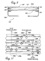
- Fig. 9 is a schematic partial cross-sectional view of a plasma generating chamber in accordance with another embodiment of the present invention utilizing dual coils, one of which is RF powered for plasma generation and the other of which is DC biased to provide a supplemental target.
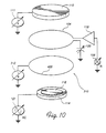
- Fig. 10 is a schematic diagram of the electrical interconnections to the plasma generating chamber of Fig. 10.
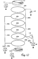
- Fig. 11 illustrates a plurality of coil ring feedthrough standoffs for a plasma generating chamber having two multiple ring coils in which the rings of the two coils are interleaved.
- Fig. 12 is a schematic diagram of the electrical interconnections to the plasma generating chamber of Fig. 11.
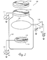
- a plasma generator in accordance with a first embodiment of the present invention comprises a substantially cylindrical plasma chamber 100 which is received in a vacuum chamber 102 (shown schematically in Fig. 2).
- the plasma chamber 100 of this embodiment has a single turn coil 104 which is carried internally by a shield 106.
- the shield 106 protects the interior walls (not shown) of the vacuum chamber 102 from the material being deposited within the interior of the plasma chamber 100.
- Radio frequency (RF) energy from an RF generator 106 is radiated from the coil 104 into the interior of the deposition system 100, which energizes a plasma within the deposition system 100.
- the energized plasma produces a plasma ion flux which strikes a negatively biased target 110 positioned at the top of the chamber 102.
- the target 110 is negatively biased by a DC power source 111.
- the plasma ions eject material from the target 110 onto a substrate 112 which may be a wafer or other workpiece which is supported by a pedestal 114 at the bottom of the deposition system 100.
- a rotating magnet assembly 116 provided above the target 110 produces magnetic fields which sweep over the face of the target 110 to promote uniform erosion of the target.
- the atoms of material ejected from the target 110 are in turn ionized by the plasma being energized by the coil 104 which is inductively coupled to the plasma.
- the RF generator 106 is preferably coupled to the coil 104 through an amplifier and impedance matching network 118.
- the other end of the coil 104 is coupled to ground, preferably through a capacitor 120 which may be a variable capacitor.
- the ionized deposition material is attracted to the substrate 112 and forms a deposition layer thereon.
- the pedestal 114 may be negatively biasd by an AC (or DC or RF) source 121 so as to externally bias the substrate 112.
- material is also sputtered from the coil 104 onto the substrate 112 to supplement the material which is being sputtered from the target 110 onto the workpiece.
- the layer deposited onto the substrate 112 is formed from material from both the coil 104 and the target 110 which can substantially improve the uniformity of the resultant layer.
- the coil 104 is carried on the shield 106 by a plurality of coil standoffs 122 (Fig. 1) which electrically insulate the coil 104 from the supporting shield 106.
- a plurality of coil standoffs 122 FIG. 1 which electrically insulate the coil 104 from the supporting shield 106.
- the insulating coil standoffs 122 have an internal labyrinth structure which permits repeated deposition of conductive materials from the target 110 onto the coil standoffs 122 while preventing the formation of a complete conducting path of deposited material from the coil 104 to the shield 106 which could short the coil 104 to the shield 106 (which is typically at ground).
- RF power is applied to the coil 104 by feedthroughs (not shown) which are supported by insulating feedthrough standoffs 124.
- the feedthrough standoffs 124 like the coil support standoffs 122, permit repeated deposition of conductive material from the target onto the feedthrough standoff 124 without the formation of a conducting path which could short the coil 104 to the shield 106.
- the coil feedthrough standoff 124 has an internal labyrinth structure somewhat similar to that of the coil standoff 122 to prevent the formation of a short between the coil 104 and the wall 140 of the shield.
- the plasma chamber 100 has a dark space shield ring 130 which provides a ground plane with respect to the target 110 above which is negatively biased.
- the shield ring 130 shields the outer edges of the target from the plasma to reduce sputtering of the target outer edges.
- the dark space shield 130 performs yet another function in that it is positioned to shield the coil 104 (and the coil support standoffs 122 and feedthrough standoffs 124) from the material being sputtered from the target 110.
- the dark space shield 130 does not completely shield the coil 104 and its associated supporting structure from all of the material being sputtered since some of the sputtered material travels at an oblique angle with respect to the vertical axis of the plasma chamber 100. However, because much of the sputtered material does travel parallel to the vertical axis of the chamber or at relatively small oblique angles relative to the vertical axis, the dark space shield 130 which is positioned in an overlapping fashion above the coil 104, prevents a substantial amount of sputtered material from being deposited on the coil 104. By reducing the amount of material that would otherwise be deposited on the coil 104, the generation of particles by the material which is deposited on the coil 104 (and its supporting structures) can be substantially reduced.
- the dark space shield 130 is a closed continuous ring of titanium (where titanium deposition is occurring in the chamber 100) or stainless steel having a generally inverted frusto-conical shape.
- the dark space shield extends inward toward the center of plasma chamber 100 so as to overlap the coil 104 by a distance of 1/4 inch. It is recognized, of course, that the amount of overlap can be varied depending upon the relative size and placement of the coil and other factors. For example, the overlap may be increased to increase the shielding of the coil 104 from the sputtered material but increasing the overlap could also further shield the target from the plasma which may be undesirable in some applications.
- the coil 104 may be placed in a recessed coil chamber (not shown) to further protect the coil and reduce particle deposits on the workpiece.
- the chamber shield 106 is generally bowl-shaped and includes a generally cylindrically shaped, vertically oriented wall 140 to which the standoffs 122 and 124 are attached to insulatively support the coil 104.
- the shield further has a generally annular-shaped floor wall (not shown) which surrounds the chuck or pedestal 114 which supports the workpiece 112 which has an 8" diameter in the illustrated embodiment.
- a clamp ring (not shown) may be used to clamp the wafer to the chuck 114 and cover the gap between the floor wall of the shield 106 and the chuck 114.
- the plasma chamber 100 is supported by an adapter ring assembly 152 which engages the vacuum chamber.
- the chamber shield 106 is grounded to the system ground through the adapter ring assembly 152.
- the dark space shield 130 like the chamber shield 106, is grounded through the adapter ring assembly 152.
- the target 110 is generally disk-shaped and is also supported by the adapter ring assembly 152. However, the target 110 is negatively biased and therefore should be insulated from the adapter ring assembly 152 which is at ground. Accordingly, seated in a circular channel formed in the underside of the target 110 is a ceramic insulation ring assembly 172 which is also seated in a corresponding channel 174 in the upper side of the target 152.
- the insulator ring assembly 172 which may be made of a variety of insulative materials including ceramics spaces the target 110 from the adapter ring assembly 152 so that the target 110 may be adequately negatively biased.
- the target, adapter and ceramic ring assembly are provided with O-ring sealing surfaces (not shown) to provide a vacuum tight assembly from the vacuum chamber to the target 110.
- the coil 104 of the illustrated embodiment is made of 1/2 by 1/8 inch heavy duty bead blasted solid high-purity (preferably 99.995% pure) titanium ribbon formed into a single turn coil having a diameter of 10-12 inches.
- the ribbon may be as thin as 1/16 inch and exceed 2 inches in height.
- both the target and the coil may be made of high purity aluminum.
- hollow tubing may be utilized, particularly if water cooling is desired.
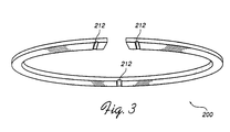
- each turn of the coil may be implemented with a flat, open-ended annular ring such as that illustrated at 200 in Fig. 3.
- a flat, open-ended annular ring such as that illustrated at 200 in Fig. 3.
- Such an arrangement is particularly advantageous for multiple turn coils.
- the advantage of a multiple turn coil is that the required current levels can be substantially reduced for a given RF power level.
- multiple turn coils tend to be more complicated and hence most costly and difficult to clean as compared to single turn coils.
- a three turn helical coil of titanium and its associated supporting structure could be quite expensive.
- the cost of manufacture of a multiple turn coil can be substantially reduced by utilizing several such flat rings 200a-200c to form a multiple turn coil 104' as illustrated in Fig. 4.
- Each ring is supported on one side by a support standoff 204a-204c and a pair of RF feedthrough standoffs 206a-206c and 208a-208c (Fig. 6) on the other side.
- the support standoffs 204a-204c are preferably positioned on the shield wall 210 in a staggered relationship.
- Each support standoff 204a-204c is received by a corresponding groove 212 (Fig. 3) formed in the underside of the corresponding coil ring 200 to secure the coil ring in place.
- the coil rings 200a-200c are electrically connected together in series by RF feedthroughs which pass through the RF feedthrough standoffs 206a-206c and 208a-208c.
- the feedthrough standoffs 206a-206c and 208a-208c are each received in a corresponding groove 212 (Fig. 3) formed in the underside of each coil ring adjacent each end of the coil ring.
- a corresponding groove 212 FIG. 3
- an RF waveguide 220a external to the shield wall is coupled by the RF feedthrough in feedthrough standoff 206a to one end of the lowest coil ring 200a.
- the other end of the coil ring 200a is coupled by the RF feedthrough in feedthrough standoff 208a to another external RF waveguide 220b which is coupled by the RF feedthrough in feedthrough standoff 206b to one end of the middle coil ring 200b.
- the other end of the coil ring 200b is coupled by the RF feedthrough in feedthrough standoff 208b to another extemal RF waveguide 220c which is coupled by the RF feedthrough in feedthrough standoff 206c to one end of the top coil ring 200c.
- the other end of the top coil ring 200c is coupled by the RF feedthrough in feedthrough standoff 208c to another extemal RF waveguide 220d.
- the currents through the coil rings 200a-200c will be directed in the same direction such that the magnetic fields generated by the coil rings will constructively reinforce each other. Because the coil 104' is a multiple turn coil, the current handling requirements of the feedthrough supports 206 and 208 can be substantially reduced as compared to those of the feedthrough supports 124 of the single turn coil 104 for a given RF power level.
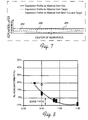
- the deposition level of the material being sputtered from the coil 104 can be selected in such a manner as to compensate substantially for the nonuniformity of the deposition profile of the material from the target such that the overall deposition profile of the layer from both sources of sputtered material as indicated by the deposition profile 254 in Fig. 7 can be substantially more uniform than that which has often been obtained from the target alone.
- the coil supply sufficient sputtered material such that the material sputtered from the coil be deposited at a rate of at least 50 ⁇ per minute as measured at the edge of the wafer in addition to that material being sputtered from the target and deposited on the wafer.
- the amount of sputtering which originates from the coil 104 as compared to the sputtering which originates from the target 110 is a function of the RF power applied to the coil 104 relative to the DC power applied to the target 110.
- the ratio of the coil RF power to the target DC power By adjusting the ratio of the coil RF power to the target DC power, the relative amounts of material sputtered from the coil 104 and the target 110 may be varied so as to achieve the desired uniformity.
- a particular ratio of the coil RF power to the target DC power will achieve the smallest degree (represented as 0%) of non-uniformity of the layer of material deposited from both the coil and the target.
- the deposited layer tends to be more edge thick as represented by the increasingly negative percentage of non-uniformity as shown in Fig. 8.
- an edge thick non-uniformity was chosen to be represented by a negative percentage of non-uniformity and a center thick non-uniformity was chosen to be represented by a positive percentage of non-uniformity.
- the center of the deposited layer tends to grow increasingly thicker relative to the edges as represented by the increasingly positive percentage of non-uniformity.
- the ratio of the RF power to the coil relative to the DC power biasing the target the material being sputtered from the coil can be increased or decreased as appropriate to effectively compensate for non-uniformity of the material being deposited from the target to achieve a more uniform deposited layer comprising material from both the target and the coil.
- a coil RF power to target DC power ratio of approximately 1.5 has been found to provide satisfactory results on an 8 inch diameter wafer.
- Fig. 8 depicts the results of varying coil RF power to target DC power for a three turn coil in which a ratio of approximately 0.7 is indicated as being optimal.
- the relative amounts of sputtering between the coil and the target may also be a function of the DC biasing of the coil 104 relative to that of the target 110.
- This DC biasing of the coil 104 may be adjusted in a variety of methods.
- the matching network 302 typically includes inductors and capacitors. By varying the capacitance of one or more capacitors of the matching network, the DC biasing of the coil 104 might be adjusted to achieve the desired level of uniformity.
- the RF power to the coil and the DC biasing of the coil 104 may have separate adjustment inputs to achieve the desired results.
- An alternative power arrangement could include two RF generators operated at slightly different frequencies.
- the output of one generator would be coupled to the coil in the conventional manner but the other generator at the slightly different frequency would be capacitively coupled to the coil such that a change in the power level of the second generator would change the DC bias of the coil.
- Such an arrangement could provide independent control of the RF power and DC bias applied to the coil. At present, it is believed that relatively large changes in DC bias to the coil for a given RF power level would be necessary to have a substantial effect on the amount of material sputtered from the coil.
- each of the embodiments discussed above utilized a single coil in the plasma chamber. It should be recognized that the present invention is applicable to plasma chambers having more than one RF powered coil. For example, the present invention may be applied to multiple coil chambers for launching helicon waves of the type described in copending application serial No.08/559,345.
- the appropriate RF generators and matching circuits are components well known to those skilled in the art.
- an RF generator such as the ENI Genesis series which has the capability to "frequency hunt" for the best frequency match with the matching circuit and antenna is suitable.
- the frequency of the generator for generating the RF power to the coil 104 is preferably 2 MHz but it is anticipated that the range can vary from, for example, 1 MHz to 100 MHz.
- An RF power setting of 4.5 kW is preferred but a range of 1.5-5 kW is believed to be satisfactory.
- energy may also be transferred to the plasma by applying AC or DC power to coils and other energy transfer members.
- a DC power setting for biasing the target 110 of 3 kW is preferred but a range of 2-5 kW and a pedestal bias voltage of -30 volts DC is believed to be satisfactory for many applications.
- the shield 106 has a diameter of 13 1/2" but it is anticipated that good results can be obtained so long as the shield has a diameter sufficient to extend beyond the outer diameter of the target, the substrate support and substrate, to shield the chamber from the plasma.
- the shields may be fabricated from a variety of materials including insulative materials such as ceramics or quartz.
- the shield and all metal surfaces likely to be coated with the target material are preferably made of the same material as the sputtered target material but may be made of a material such as stainless steel or copper.
- the material of the structure which will be coated should have a coefficient of thermal expansion which closely matches that of the material being sputtered to reduce flaking of sputtered material from the shield or other structure onto the wafer.
- the material to be coated should have good adhesion to the sputtered material.
- the preferred metal of the shields, brackets and other structures likely to be coated is bead blasted titanium. Any surfaces which are more likely to sputter such as the end caps of the coil support and feed through standoffs would preferably be made of the same type of material as the target such as high purity titanium, for example.
- the material to be deposited is a material other than titanium, the preferred metal is the deposited material, stainless steel or copper. Adherence can also be improved by coating the structures with molybdenum prior to sputtering the target. However, it is preferred that the coil (or any other surface likely to sputter) not be coated with molybdenum or other materials since the molybdenum can contaminate the workpiece if sputtered from the coil.
- the wafer to target space is preferably about 140 mm but can range from about 1.5" to 8".
- satisfactory coverage i.e., the ratio of aperture bottom deposition thickness to field deposition thickness
- a coil diameter of about 11 1/2 inches spaced from the target by a distance of about 2.9 inches. It has been found that increasing the diameter of the coil which moves the coil away from the workpiece edge has an adverse effect on bottom coverage.
- decreasing the coil diameter to move the coil closer to the wafer edge can adversely effect layer uniformity. It is believed that decreasing the coil diameter causes the coil to be more closely aligned with the target resulting in substantial deposition of material from the target onto the coil which in turn can adversely effect the uniformity of material being sputtered from the coil.
- Deposition uniformity also appears to be a function of coil spacing from the target. As previously mentioned, a spacing of about 2.9 inches between the coil and target has been found satisfactory for a target to wafer spacing of 140 mm. Moving the coil vertically either toward or away from the target (or wafer) can adversely effect deposition layer uniformity.
- Fig. 9 illustrates an alternative embodiment of a plasma chamber 100" having a coil 104" formed of a single open ended coil ring 200d of the type depicted in Fig. 3. As shown in Fig.
- the coil 104" is coupled through the shield 308 by feedthrough standoffs 206 to a matching network 118 and an RF generator 106 in the same manner as the coils 104 and 104' described above.
- the chamber 100" has a second target 310 which, although generally shaped like a coil, is not coupled to an RF generator. Instead, the second target 310 formed of a flat closed ring 400 is coupled through feedthrough standoffs 206 to a variable negative DC bias source 312 as shown in Fig. 10.
- the chamber has three "targets," the first and second targets 110 and 310, respectively, as well as the RF coil 104". However, most of the material sputtered from the coil 104" and the second target 310 originates from the DC biased target 310 rather than the RF powered coil 104".
- the relative amounts of material being sputtered from the coil 104" and the first and second targets 110 and 310 are a function primarily of the relative DC power biasing the target 310 and the target 110.
- the variable DC power sources 111 and 312 biasing the first target 110 and the second target 310, respectively can be set to optimize the uniformity of the deposition of material more independently of the RF power setting for the RF generator 106 powering the coil 104".
- the RF power to the coil 104" can be set more independently of the DC biases to the target 110 and the target 310 in order to optimize plasma density for ionization purposes.
- the RF power levels for the coil 104" may be lower as compared to those for the coil 104.
- a suitable power range for the coil 104" is 1.5 to 3.5 kW RF.
- the power ranges for the primary target 110 and the secondary target, i.e., the coil 310, are 2-5 kW DC and 1-3 kW DC, respectively. Of course, values will vary depending upon the particular application.
- Figs. 11 and 12 show yet another alternative embodiment, which includes a multiple turn RF coil and a multiple ring secondary target in which the rings of the target are interleaved with the turns of the RF coil.
- the RF coil of Fig. 12 like the coil 104' of Figs 4-6, is formed of flat rings 200a-200c which are electrically connected together in series by RF feedthroughs which pass through the RF feedthrough standoffs 206a-206c and 208a-208c and extemal waveguides 220a-220d to the RF source and RF ground.
- the negatively biasing DC power source 312 extemal to the shield wall is coupled by an external strap 330a to a DC feedthrough in feedthrough standoff 206d to the lowest ring 400a of the second sputtering target.
- the target ring 400a is also coupled by the DC feedthrough in feedthrough standoff 206d to another extemal DC strap 330b which is coupled by the DC feedthrough in feedthrough standoff 206e to the middle target ring 400b.
- the target ring 400b is also coupled by the DC feedthrough in feedthrough standoff 206e to another external strap 330c which is coupled by the DC feedthrough in feedthrough standoff 206f to the top target ring 400c of sputtering secondary target.
- the target rings 400a-400c of the target 310' will be negatively DC biased so that the majority of the material sputtered from the RF coil and the secondary 400a-400c target will originate primarily from the target rings 400a-400c of the secondary target.
- the RF coil is a multiple turn coil
- the current handling requirements of the feedthrough supports 206 and 208 can be substantially reduced as compared to those of the feedthrough supports 124 of the single turn coil 104 for a given RF power level as set forth above.
- the life of the sputtering rings can be enhanced as a result of using multiple rings.
- the secondary sputtering targets 310 and 400a-400c have been described as being fabricated from flat rings 400, it should be appreciated that the sputtering secondary targets may be fabricated from ribbon and tubular materials as well as in a variety of other shapes and sizes including cylinders and segments of cylinders. However, it is preferred that the secondary targets be shaped so as to be symmetrical about the axis of the substrate and encircle the interior of the chamber at the periphery of the plasma.
- the secondary target material should be a solid, conductive material and may be of the same type or a different type of conductive material than that of the primary target 110.
- the biasing of the primary and secondary targets has been described as DC biasing, it should be appreciated that in some applications, AC or RF biasing of one or both of the primary and secondary targets may be appropriate.
- precursor gases may be utilized to generate the plasma including Ar, H 2 or reactive gases such as NF 3 , CF 4 and many others.
- Various precursor gas pressures are suitable induding pressures of 0.1 - 50 mTorr. For ionized PVD, a pressure between 10 and 100 mTorr is preferred for best ionization of sputtered material.
Abstract
A sputtering coil for a plasma chamber (100) in a semiconductor fabrication system is provided. The sputtering coil (104) couples energy into a plasma and also provides a source of sputtering material to be sputtered onto a workpiece (112) from the coil to supplement material being sputtered from a target (110) onto the workpiece. Alternatively a plurality of coils may be provided, one primarily for coupling energy into the plasma and the other primarily for providing a supplemental source of sputtering material to be sputtered on the workpiece.
Description
- The present invention relates to plasma generators, and more particularly, to a method and apparatus for generating a plasma to sputter deposit a layer of material in the fabrication of semiconductor devices.
- Low pressure radio frequency (RF) generated plasmas have become convenient sources of energetic ions and activated atoms which can be employed in a variety of semiconductor device fabrication processes including surface treatments, depositions, and etching processes. For example, to deposit materials onto a semiconductor wafer using a sputter deposition process, a plasma is produced in the vicinity of a sputter target material which is negatively biased. Ions created within the plasma impact the surface of the target to dislodge, i.e., "sputter" material from the target. The sputtered materials are then transported and deposited on the surface of the semiconductor wafer.
- Sputtered material has a tendency to travel in straight line paths from the target to the substrate being deposited at angles which are oblique to the surface of the substrate. As a consequence, materials deposited in etched trenches and holes of semiconductor devices having trenches or holes with a high depth to width aspect ratio, can bridge over causing undesirable cavities in the deposition layer. To prevent such cavities, the sputtered material can be redirected into substantially vertical paths between the target and the substrate by negatively charging the substrate and positioning appropriate vertically oriented electric fields adjacent the substrate if the sputtered material is sufficiently ionized by the plasma. However, material sputtered by a low density plasma often has an ionization degree of less than 1% which is usually insufficient to avoid the formation of an excessive number of cavities. Accordingly, it is desirable to increase the density of the plasma to increase the ionization rate of the sputtered material in order to decrease the formation of unwanted cavities in the deposition layer. As used herein, the term "dense plasma" is intended to refer to one that has a high electron and ion density.
- There are several known techniques for exciting a plasma with RF fields including capacitive coupling, inductive coupling and wave heating. In a standard inductively coupled plasma (ICP) generator, RF current passing through a coil surrounding the plasma induces electromagnetic currents in the plasma. These currents heat the conducting plasma by ohmic heating, so that it is sustained in steady state. As shown in U.S. Pat. No. 4,362,632, for example, current through a coil is supplied by an RF generator coupled to the coil through an impedance matching network, such that the coil acts as the first windings of a transformer. The plasma acts as a single turn second winding of a transformer.
- In many high density plasma applications, it is preferable for the chamber to be operated at a relatively high pressure so that the frequency of collisions between the plasma ions and the deposition material atoms is increased to increase thereby the resident time of the sputtered material in the high density plasma zone. However, scattering of the deposition atoms is likewise increased. This scattering of the deposition atoms typically causes the thickness of the deposition layer on the substrate to be thicker on that portion of the substrate aligned with the center of the target and thinner in the outlying regions. It has been found that the deposition layer can be made more uniform by reducing the distance between the target and the substrate which reduces the effect of the plasma scattering.
- On the other hand, in order to increase the ionization of the plasma to increase the sputtering rate and the ionization of the sputtered atoms, it has been found desirable to increase the distance between the target and the substrate. The coil which is used to couple energy into the plasma typically encircles the space between the target and the substrate. If the target is positioned too closely to the substrate, the ionization of the plasma can be adversely affected. Thus, in order to accommodate the coil which is coupling RF energy into the plasma, it has often been found necessary to space the target from the substrate a certain minimum distance even though such a minimum spacing can have an adverse effect on the uniformity of the deposition.
- It is an object of the present invention to provide an improved method and apparatus for generating a plasma within a chamber and for sputter depositing a layer which obviate, for practical purposes, the above-mentioned limitations.
- These and other objects and advantages are achieved by, in accordance with one aspect of the invention, a plasma generating apparatus which inductively couples electromagnetic energy from a coil which is also adapted to sputter material from the coil onto the workpiece to supplement the material being sputtered from a target onto the workpiece. The coil is preferably made of the same type of material as the target so that the atoms sputtered from the coil combine with the atoms sputtered from the target to form a layer of the desired type of material. It has been found that the distribution of material sputtered from a coil in accordance with one embodiment of the present invention tends to be thicker at the edges of the substrate and thinner toward the center of the substrate. Such a distribution is very advantageous for compensating for the distribution profile of material sputtered from a target in which the material from the target tends to deposit more thickly in the center of the substrate as compared to the edges. As a consequence, the materials deposited from both the coil and the target can combine to form a layer of relatively uniform thickness from the center of the substrate to its edges.
- In one embodiment, both the target and the coil are formed from relatively pure titanium so that the material sputtered onto the substrate from both the target and the coil is substantially the same material, that is, titanium. In other embodiments, other types of materials may be deposited such as aluminum. In which case, the coil as well as the target would be made from the same grade of aluminum, i.e., target grade aluminum. If it is desired to deposit a mixture or combination of materials, the target and the coil can be formed from the same mixture of materials or alternatively from different materials such that the materials combine or mix when deposited on the substrate.
- In yet another embodiment, a second coil-like structure in addition to the first coil, provides a supplemental target for sputtering material. This second coil is preferably not coupled to an RF generator but is instead biased with DC power. Although material may or may not continue to be sputtered from the first coil, sputtered material from the coils will originate primarily from the second coil because of its DC biasing. Such an arrangement permits the ratio of the DC bias of the primary target to the DC bias of the second coil to be set to optimize compensation for non-uniformity in thickness of the material being deposited from the primary target. In addition, the RF power applied to the first coil can be set independently of the biases applied to the target and the second coil for optimization of the plasma density for ionization.
- The following is a description of some specific embodiments of the invention, reference being made to the accompanying drawings, in which:
- Fig. 1 is a perspective, partial cross-sectional view of a plasma generating chamber in accordance with one embodiment of the present invention.
- Fig. 2 is a schematic diagram of the electrical interconnections to the plasma generating chamber of Fig. 1.
- Fig. 3 is a perspective view of a coil ring for a plasma generating apparatus in accordance with another embodiment of the present invention.
- Fig. 4 is a schematic partial cross-sectional view of a plasma generating chamber in accordance with another embodiment of the present invention utilizing a coil ring as shown in Fig. 3.
- Fig. 5 illustrates a plurality of coil ring support standoffs for the plasma generating chamber of Fig. 4.
- Fig. 6 illustrates a plurality of coil ring feedthrough standoffs for the plasma generating chamber of Fig. 4.
- Fig. 7 is a chart depicting the respective deposition profiles for material deposited from the coil and the target of the apparatus of Fig. 1.
- Fig. 8 is a graph depicting the effect on deposition uniformity of the ratio of the RF power applied to the coil relative to the DC power bias of the target.
- Fig. 9 is a schematic partial cross-sectional view of a plasma generating chamber in accordance with another embodiment of the present invention utilizing dual coils, one of which is RF powered for plasma generation and the other of which is DC biased to provide a supplemental target.
- Fig. 10 is a schematic diagram of the electrical interconnections to the plasma generating chamber of Fig. 10.
- Fig. 11 illustrates a plurality of coil ring feedthrough standoffs for a plasma generating chamber having two multiple ring coils in which the rings of the two coils are interleaved.
- Fig. 12 is a schematic diagram of the electrical interconnections to the plasma generating chamber of Fig. 11.
- Referring first to Figs. 1 and 2, a plasma generator in accordance with a first embodiment of the present invention comprises a substantially
cylindrical plasma chamber 100 which is received in a vacuum chamber 102 (shown schematically in Fig. 2). Theplasma chamber 100 of this embodiment has asingle turn coil 104 which is carried internally by ashield 106. Theshield 106 protects the interior walls (not shown) of thevacuum chamber 102 from the material being deposited within the interior of theplasma chamber 100. - Radio frequency (RF) energy from an
RF generator 106 is radiated from thecoil 104 into the interior of thedeposition system 100, which energizes a plasma within thedeposition system 100. The energized plasma produces a plasma ion flux which strikes a negativelybiased target 110 positioned at the top of thechamber 102. Thetarget 110 is negatively biased by aDC power source 111. The plasma ions eject material from thetarget 110 onto asubstrate 112 which may be a wafer or other workpiece which is supported by apedestal 114 at the bottom of thedeposition system 100. A rotatingmagnet assembly 116 provided above thetarget 110 produces magnetic fields which sweep over the face of thetarget 110 to promote uniform erosion of the target. - The atoms of material ejected from the
target 110 are in turn ionized by the plasma being energized by thecoil 104 which is inductively coupled to the plasma. TheRF generator 106 is preferably coupled to thecoil 104 through an amplifier andimpedance matching network 118. The other end of thecoil 104 is coupled to ground, preferably through acapacitor 120 which may be a variable capacitor. The ionized deposition material is attracted to thesubstrate 112 and forms a deposition layer thereon. Thepedestal 114 may be negatively biasd by an AC (or DC or RF)source 121 so as to externally bias thesubstrate 112. As set forth in greater detail in copending application Serial No. , filed July 9, 1996 (Attorney Docket No. 1402/PVD/DV), Express Mail Certificate No. EM 129 431 588, entitled "Method for Providing Full-Face High Density Plasma Deposition" by Ken Ngan, Simon Hui and Gongda Yao, which is assigned to the assignee of the present application and is incorporated herein by reference in its entirety, external biasing of thesubstrate 112 may optionally be eliminated. - As will be explained in greater detail below, in accordance with one aspect of the present invention, material is also sputtered from the
coil 104 onto thesubstrate 112 to supplement the material which is being sputtered from thetarget 110 onto the workpiece. As a result, the layer deposited onto thesubstrate 112 is formed from material from both thecoil 104 and thetarget 110 which can substantially improve the uniformity of the resultant layer. - The
coil 104 is carried on theshield 106 by a plurality of coil standoffs 122 (Fig. 1) which electrically insulate thecoil 104 from the supportingshield 106. As set forth in greater detail in copending application Serial No. 081647,182, entitled Recessed Coil for Generating a Plasma, filed May 9, 1996 (Attorney Docket # 1186/PVD/DV) and assigned to the assignee of the present application, which application is incorporated herein by reference in its entirety, the insulatingcoil standoffs 122 have an internal labyrinth structure which permits repeated deposition of conductive materials from thetarget 110 onto thecoil standoffs 122 while preventing the formation of a complete conducting path of deposited material from thecoil 104 to theshield 106 which could short thecoil 104 to the shield 106 (which is typically at ground). - RF power is applied to the
coil 104 by feedthroughs (not shown) which are supported by insulatingfeedthrough standoffs 124. The feedthrough standoffs 124, like thecoil support standoffs 122, permit repeated deposition of conductive material from the target onto thefeedthrough standoff 124 without the formation of a conducting path which could short thecoil 104 to theshield 106. Thus, thecoil feedthrough standoff 124 has an internal labyrinth structure somewhat similar to that of thecoil standoff 122 to prevent the formation of a short between thecoil 104 and the wall 140 of the shield. - As best seen in Fig. 1, the
plasma chamber 100 has a darkspace shield ring 130 which provides a ground plane with respect to thetarget 110 above which is negatively biased. In addition, as explained in greater detail in the aforementioned copending application Serial No. 08/647,182, theshield ring 130 shields the outer edges of the target from the plasma to reduce sputtering of the target outer edges. Thedark space shield 130 performs yet another function in that it is positioned to shield the coil 104 (and thecoil support standoffs 122 and feedthrough standoffs 124) from the material being sputtered from thetarget 110. Thedark space shield 130 does not completely shield thecoil 104 and its associated supporting structure from all of the material being sputtered since some of the sputtered material travels at an oblique angle with respect to the vertical axis of theplasma chamber 100. However, because much of the sputtered material does travel parallel to the vertical axis of the chamber or at relatively small oblique angles relative to the vertical axis, thedark space shield 130 which is positioned in an overlapping fashion above thecoil 104, prevents a substantial amount of sputtered material from being deposited on thecoil 104. By reducing the amount of material that would otherwise be deposited on thecoil 104, the generation of particles by the material which is deposited on the coil 104 (and its supporting structures) can be substantially reduced. - In the illustrated embodiment, the
dark space shield 130 is a closed continuous ring of titanium (where titanium deposition is occurring in the chamber 100) or stainless steel having a generally inverted frusto-conical shape. The dark space shield extends inward toward the center ofplasma chamber 100 so as to overlap thecoil 104 by a distance of 1/4 inch. It is recognized, of course, that the amount of overlap can be varied depending upon the relative size and placement of the coil and other factors. For example, the overlap may be increased to increase the shielding of thecoil 104 from the sputtered material but increasing the overlap could also further shield the target from the plasma which may be undesirable in some applications. In an alternative embodiment, thecoil 104 may be placed in a recessed coil chamber (not shown) to further protect the coil and reduce particle deposits on the workpiece. - The
chamber shield 106 is generally bowl-shaped and includes a generally cylindrically shaped, vertically oriented wall 140 to which thestandoffs coil 104. The shield further has a generally annular-shaped floor wall (not shown) which surrounds the chuck orpedestal 114 which supports theworkpiece 112 which has an 8" diameter in the illustrated embodiment. A clamp ring (not shown) may be used to clamp the wafer to thechuck 114 and cover the gap between the floor wall of theshield 106 and thechuck 114. - The
plasma chamber 100 is supported by anadapter ring assembly 152 which engages the vacuum chamber. Thechamber shield 106 is grounded to the system ground through theadapter ring assembly 152. Thedark space shield 130, like thechamber shield 106, is grounded through theadapter ring assembly 152. - The
target 110 is generally disk-shaped and is also supported by theadapter ring assembly 152. However, thetarget 110 is negatively biased and therefore should be insulated from theadapter ring assembly 152 which is at ground. Accordingly, seated in a circular channel formed in the underside of thetarget 110 is a ceramicinsulation ring assembly 172 which is also seated in acorresponding channel 174 in the upper side of thetarget 152. Theinsulator ring assembly 172 which may be made of a variety of insulative materials including ceramics spaces thetarget 110 from theadapter ring assembly 152 so that thetarget 110 may be adequately negatively biased. The target, adapter and ceramic ring assembly are provided with O-ring sealing surfaces (not shown) to provide a vacuum tight assembly from the vacuum chamber to thetarget 110. - The
coil 104 of the illustrated embodiment is made of 1/2 by 1/8 inch heavy duty bead blasted solid high-purity (preferably 99.995% pure) titanium ribbon formed into a single turn coil having a diameter of 10-12 inches. However, other highly conductive materials and shapes may be utilized depending upon the material being sputtered and other factors. For example, the ribbon may be as thin as 1/16 inch and exceed 2 inches in height. Also, if the material to be sputtered is aluminum, both the target and the coil may be made of high purity aluminum. In addition to the ribbon shape illustrated, hollow tubing may be utilized, particularly if water cooling is desired. - Still further, instead of the ribbon shape illustrated, each turn of the coil, where the coil has multiple turns, may be implemented with a flat, open-ended annular ring such as that illustrated at 200 in Fig. 3. Such an arrangement is particularly advantageous for multiple turn coils. The advantage of a multiple turn coil is that the required current levels can be substantially reduced for a given RF power level. However, multiple turn coils tend to be more complicated and hence most costly and difficult to clean as compared to single turn coils. For example, a three turn helical coil of titanium and its associated supporting structure could be quite expensive. The cost of manufacture of a multiple turn coil can be substantially reduced by utilizing several such
flat rings 200a-200c to form a multiple turn coil 104' as illustrated in Fig. 4. Each ring is supported on one side by asupport standoff 204a-204c and a pair ofRF feedthrough standoffs 206a-206c and 208a-208c (Fig. 6) on the other side. As best seen in Fig. 5, thesupport standoffs 204a-204c are preferably positioned on theshield wall 210 in a staggered relationship. Eachsupport standoff 204a-204c is received by a corresponding groove 212 (Fig. 3) formed in the underside of thecorresponding coil ring 200 to secure the coil ring in place. - The coil rings 200a-200c are electrically connected together in series by RF feedthroughs which pass through the
RF feedthrough standoffs 206a-206c and 208a-208c. In the same manner as thesupport standoffs 204a-204c, thefeedthrough standoffs 206a-206c and 208a-208c are each received in a corresponding groove 212 (Fig. 3) formed in the underside of each coil ring adjacent each end of the coil ring. As schematically represented in Fig. 6, anRF waveguide 220a external to the shield wall is coupled by the RF feedthrough infeedthrough standoff 206a to one end of thelowest coil ring 200a. The other end of thecoil ring 200a is coupled by the RF feedthrough infeedthrough standoff 208a to anotherexternal RF waveguide 220b which is coupled by the RF feedthrough infeedthrough standoff 206b to one end of themiddle coil ring 200b. The other end of thecoil ring 200b is coupled by the RF feedthrough infeedthrough standoff 208b to anotherextemal RF waveguide 220c which is coupled by the RF feedthrough infeedthrough standoff 206c to one end of thetop coil ring 200c. Finally, the other end of thetop coil ring 200c is coupled by the RF feedthrough infeedthrough standoff 208c to anotherextemal RF waveguide 220d. Coupled together in this manner, it is seen that the currents through the coil rings 200a-200c will be directed in the same direction such that the magnetic fields generated by the coil rings will constructively reinforce each other. Because the coil 104' is a multiple turn coil, the current handling requirements of the feedthrough supports 206 and 208 can be substantially reduced as compared to those of the feedthrough supports 124 of thesingle turn coil 104 for a given RF power level. - As previously mentioned, in order to accommodate the
coil 104 to facilitate ionization of the plasma, it has been found beneficial to space thetarget 110 from the surface of theworkpiece 112. However, this increased spacing between the target and the workpiece can adversely impact the uniformity of the material being deposited from the target. As indicated at 250 in Fig. 7, such nonuniformity typically exhibits itself as a thickening of the deposited material toward the center of the workpiece with a consequent thinning of the deposited material toward the edges of the workpiece. In accordance with one feature of the present invention, this nonuniformity can be effectively compensated by sputtering deposition material not only from thesputter target 110 above the workpiece but also from thecoil 104 encircling the edges of the workpiece. Because the edges of the workpiece are closer to thecoil 104 than is the center of the workpiece, it has been found that the material sputtered from the coil tends to deposit more thickly toward the edges of the workpiece than the center, as indicated at 252 in Fig. 3. This is of course the reverse of the deposition pattern of material from thetarget 110. By appropriately adjusting the ratio of RF power level applied to thecoil 104 to the DC power level of the bias applied to the target, it has been found that the deposition level of the material being sputtered from thecoil 104 can be selected in such a manner as to compensate substantially for the nonuniformity of the deposition profile of the material from the target such that the overall deposition profile of the layer from both sources of sputtered material as indicated by thedeposition profile 254 in Fig. 7 can be substantially more uniform than that which has often been obtained from the target alone. It is preferred that the coil supply sufficient sputtered material such that the material sputtered from the coil be deposited at a rate of at least 50 Å per minute as measured at the edge of the wafer in addition to that material being sputtered from the target and deposited on the wafer. - It is presently believed that the amount of sputtering which originates from the
coil 104 as compared to the sputtering which originates from thetarget 110 is a function of the RF power applied to thecoil 104 relative to the DC power applied to thetarget 110. By adjusting the ratio of the coil RF power to the target DC power, the relative amounts of material sputtered from thecoil 104 and thetarget 110 may be varied so as to achieve the desired uniformity. As shown in Fig. 8, it is believed that a particular ratio of the coil RF power to the target DC power will achieve the smallest degree (represented as 0%) of non-uniformity of the layer of material deposited from both the coil and the target. As the RF power to the coil is increased relative to the DC power applied to the target, the deposited layer tends to be more edge thick as represented by the increasingly negative percentage of non-uniformity as shown in Fig. 8. (In the sign convention of Fig. 8, an edge thick non-uniformity was chosen to be represented by a negative percentage of non-uniformity and a center thick non-uniformity was chosen to be represented by a positive percentage of non-uniformity. The larger the absolute value of the percentage non-uniformity, the greater the degree of non-uniformity (either edge thick or center thick) represented by that percentage. Conversely, by decreasing the ratio of the RF power to the coil relative to the DC power applied to the target, the center of the deposited layer tends to grow increasingly thicker relative to the edges as represented by the increasingly positive percentage of non-uniformity. Thus, by adjusting the ratio of the RF power to the coil relative to the DC power biasing the target, the material being sputtered from the coil can be increased or decreased as appropriate to effectively compensate for non-uniformity of the material being deposited from the target to achieve a more uniform deposited layer comprising material from both the target and the coil. For thesingle turn coil 104, a coil RF power to target DC power ratio of approximately 1.5 has been found to provide satisfactory results on an 8 inch diameter wafer. Fig. 8 depicts the results of varying coil RF power to target DC power for a three turn coil in which a ratio of approximately 0.7 is indicated as being optimal. - It is further believed that the relative amounts of sputtering between the coil and the target may also be a function of the DC biasing of the
coil 104 relative to that of thetarget 110. This DC biasing of thecoil 104 may be adjusted in a variety of methods. For example, the matching network 302 typically includes inductors and capacitors. By varying the capacitance of one or more capacitors of the matching network, the DC biasing of thecoil 104 might be adjusted to achieve the desired level of uniformity. In one embodiment, the RF power to the coil and the DC biasing of thecoil 104 may have separate adjustment inputs to achieve the desired results. An alternative power arrangement could include two RF generators operated at slightly different frequencies. The output of one generator would be coupled to the coil in the conventional manner but the other generator at the slightly different frequency would be capacitively coupled to the coil such that a change in the power level of the second generator would change the DC bias of the coil. Such an arrangement could provide independent control of the RF power and DC bias applied to the coil. At present, it is believed that relatively large changes in DC bias to the coil for a given RF power level would be necessary to have a substantial effect on the amount of material sputtered from the coil. - Each of the embodiments discussed above utilized a single coil in the plasma chamber. It should be recognized that the present invention is applicable to plasma chambers having more than one RF powered coil. For example, the present invention may be applied to multiple coil chambers for launching helicon waves of the type described in copending application serial No.08/559,345.
- The appropriate RF generators and matching circuits are components well known to those skilled in the art. For example, an RF generator such as the ENI Genesis series which has the capability to "frequency hunt" for the best frequency match with the matching circuit and antenna is suitable. The frequency of the generator for generating the RF power to the
coil 104 is preferably 2 MHz but it is anticipated that the range can vary from, for example, 1 MHz to 100 MHz. An RF power setting of 4.5 kW is preferred but a range of 1.5-5 kW is believed to be satisfactory. In some applications, energy may also be transferred to the plasma by applying AC or DC power to coils and other energy transfer members. A DC power setting for biasing thetarget 110 of 3 kW is preferred but a range of 2-5 kW and a pedestal bias voltage of -30 volts DC is believed to be satisfactory for many applications. - In the illustrated embodiment, the
shield 106 has a diameter of 13 1/2" but it is anticipated that good results can be obtained so long as the shield has a diameter sufficient to extend beyond the outer diameter of the target, the substrate support and substrate, to shield the chamber from the plasma. The shields may be fabricated from a variety of materials including insulative materials such as ceramics or quartz. However, the shield and all metal surfaces likely to be coated with the target material are preferably made of the same material as the sputtered target material but may be made of a material such as stainless steel or copper. The material of the structure which will be coated should have a coefficient of thermal expansion which closely matches that of the material being sputtered to reduce flaking of sputtered material from the shield or other structure onto the wafer. In addition, the material to be coated should have good adhesion to the sputtered material. Thus for example if the deposited material is titanium, the preferred metal of the shields, brackets and other structures likely to be coated is bead blasted titanium. Any surfaces which are more likely to sputter such as the end caps of the coil support and feed through standoffs would preferably be made of the same type of material as the target such as high purity titanium, for example. Of course, if the material to be deposited is a material other than titanium, the preferred metal is the deposited material, stainless steel or copper. Adherence can also be improved by coating the structures with molybdenum prior to sputtering the target. However, it is preferred that the coil (or any other surface likely to sputter) not be coated with molybdenum or other materials since the molybdenum can contaminate the workpiece if sputtered from the coil. - The wafer to target space is preferably about 140 mm but can range from about 1.5" to 8". For this wafer to target spacing, satisfactory coverage, i.e., the ratio of aperture bottom deposition thickness to field deposition thickness, has been achieved with a coil diameter of about 11 1/2 inches spaced from the target by a distance of about 2.9 inches. It has been found that increasing the diameter of the coil which moves the coil away from the workpiece edge has an adverse effect on bottom coverage. On the other hand, decreasing the coil diameter to move the coil closer to the wafer edge can adversely effect layer uniformity. It is believed that decreasing the coil diameter causes the coil to be more closely aligned with the target resulting in substantial deposition of material from the target onto the coil which in turn can adversely effect the uniformity of material being sputtered from the coil.
- Deposition uniformity also appears to be a function of coil spacing from the target. As previously mentioned, a spacing of about 2.9 inches between the coil and target has been found satisfactory for a target to wafer spacing of 140 mm. Moving the coil vertically either toward or away from the target (or wafer) can adversely effect deposition layer uniformity.
- As set forth above, the relative amounts of material sputtered from the
target 110 and thecoil 104 are a function of the ratio of the RF power applied to the coil and the DC power applied to the target. However, it is recognized that in some applications, an RF power level which is optimum for improving the uniformity of the deposited layer of materials from the coil and the target may not be optimum for generating a plasma density for ionization. Fig. 9 illustrates an alternative embodiment of aplasma chamber 100" having acoil 104" formed of a single open endedcoil ring 200d of the type depicted in Fig. 3. As shown in Fig. 10, thecoil 104" is coupled through theshield 308 by feedthroughstandoffs 206 to amatching network 118 and anRF generator 106 in the same manner as thecoils 104 and 104' described above. However, thechamber 100" has asecond target 310 which, although generally shaped like a coil, is not coupled to an RF generator. Instead, thesecond target 310 formed of a flatclosed ring 400 is coupled throughfeedthrough standoffs 206 to a variable negativeDC bias source 312 as shown in Fig. 10. As a consequence, the chamber has three "targets," the first andsecond targets RF coil 104". However, most of the material sputtered from thecoil 104" and thesecond target 310 originates from the DCbiased target 310 rather than the RF poweredcoil 104". - Such an arrangement has a number of advantages. Because most of the material sputtered from the coils originates from the
second target 310 rather than thecoil 104", the relative amounts of material being sputtered from thecoil 104" and the first andsecond targets target 310 and thetarget 110. Hence the variableDC power sources first target 110 and thesecond target 310, respectively, can be set to optimize the uniformity of the deposition of material more independently of the RF power setting for theRF generator 106 powering thecoil 104". Conversely, the RF power to thecoil 104" can be set more independently of the DC biases to thetarget 110 and thetarget 310 in order to optimize plasma density for ionization purposes. - In addition, it is believed that the RF power levels for the
coil 104" may be lower as compared to those for thecoil 104. For example, a suitable power range for thecoil 104" is 1.5 to 3.5 kW RF. The power ranges for theprimary target 110 and the secondary target, i.e., thecoil 310, are 2-5 kW DC and 1-3 kW DC, respectively. Of course, values will vary depending upon the particular application. - Figs. 11 and 12 show yet another alternative embodiment, which includes a multiple turn RF coil and a multiple ring secondary target in which the rings of the target are interleaved with the turns of the RF coil. The RF coil of Fig. 12, like the coil 104' of Figs 4-6, is formed of
flat rings 200a-200c which are electrically connected together in series by RF feedthroughs which pass through theRF feedthrough standoffs 206a-206c and 208a-208c andextemal waveguides 220a-220d to the RF source and RF ground. - Interleaved with the coil rings 200a-200c of the RF coil are the
closed rings 400a-400c of the second target. As schematically represented in Figs. 11 and 12, the negatively biasingDC power source 312 extemal to the shield wall is coupled by anexternal strap 330a to a DC feedthrough infeedthrough standoff 206d to thelowest ring 400a of the second sputtering target. Thetarget ring 400a is also coupled by the DC feedthrough infeedthrough standoff 206d to anotherextemal DC strap 330b which is coupled by the DC feedthrough infeedthrough standoff 206e to themiddle target ring 400b. Thetarget ring 400b is also coupled by the DC feedthrough infeedthrough standoff 206e to anotherexternal strap 330c which is coupled by the DC feedthrough infeedthrough standoff 206f to thetop target ring 400c of sputtering secondary target. - Coupled together in this manner, it is seen that the target rings 400a-400c of the target 310' will be negatively DC biased so that the majority of the material sputtered from the RF coil and the secondary 400a-400c target will originate primarily from the target rings 400a-400c of the secondary target. Because the RF coil is a multiple turn coil, the current handling requirements of the feedthrough supports 206 and 208 can be substantially reduced as compared to those of the feedthrough supports 124 of the
single turn coil 104 for a given RF power level as set forth above. In addition, it is believed that the life of the sputtering rings can be enhanced as a result of using multiple rings. Although the secondary sputtering targets 310 and 400a-400c have been described as being fabricated fromflat rings 400, it should be appreciated that the sputtering secondary targets may be fabricated from ribbon and tubular materials as well as in a variety of other shapes and sizes including cylinders and segments of cylinders. However, it is preferred that the secondary targets be shaped so as to be symmetrical about the axis of the substrate and encircle the interior of the chamber at the periphery of the plasma. The secondary target material should be a solid, conductive material and may be of the same type or a different type of conductive material than that of theprimary target 110. Although the biasing of the primary and secondary targets has been described as DC biasing, it should be appreciated that in some applications, AC or RF biasing of one or both of the primary and secondary targets may be appropriate. - A variety of precursor gases may be utilized to generate the plasma including Ar, H2 or reactive gases such as NF3, CF4 and many others. Various precursor gas pressures are suitable induding pressures of 0.1 - 50 mTorr. For ionized PVD, a pressure between 10 and 100 mTorr is preferred for best ionization of sputtered material.
- It will, of course, be understood that modifications of the present invention, in its various aspects, will be apparent to those skilled in the art, some being apparent only after study others being matters of routine mechanical and electronic design. Other embodiments are also possible, their specific designs depending upon the particular application. As such, the scope of the invention should not be limited by the particular embodiments herein described but should be defined only by the appended claims and equivalents thereof.
Claims (40)
- An apparatus for sputter deposition of a film layer onto a substrate, comprising:a vacuum chamber having a substrate support member maintainable therein;a first biasable target disposed in said chamber; anda second biasable target disposed in said chamber adjacent to and extending substantially around a space defined between said target and said substrate support.
- The sputter deposition apparatus of claim 1, further including a first power supply connected to said first target and a second power supply connected to said second target.
- The sputter deposition apparatus of claim 2, wherein said second power supply is an AC power supply.
- The apparatus of claim 1, further including a third biasable sputter target disposed about said space defined between said first sputter target and said substrate support.
- The apparatus of claim 4, wherein said third sputter target is DC biased.
- The apparatus of claim 1, wherein said second target inductively couples into a gas maintainable in said chamber to create a plasma therefrom.
- The apparatus of claim 6, wherein said third target is negatively biased to provide sputtering thereof by said plasma.
- The apparatus of claim 7, wherein each of said targets is of the same material.
- The apparatus of claim 1, wherein said second target is a solid member.
- The apparatus of claim 7, wherein said third target is a solid member.
- An apparatus for energizing a plasma within a semiconductor fabrication system to sputter material onto a workpiece, the apparatus comprising:a semiconductor fabrication chamber having a plasma generation area within said chamber; anda metal material coil carried by said chamber and positioned to couple energy into said plasma generation area and to sputter metal material from said coil onto said workpiece.
- The apparatus of claim 11 further comprising a target made of titanium.
- The apparatus of claim 11 further comprising a target made of a material selected from Al, Cr, Te and SiO2.
- An apparatus for energizing a plasma within a semiconductor fabrication system to sputter material onto a workpiece, the apparatus comprising:a semiconductor fabrication chamber having a plasma generation area within said chamber;a sputtering target carried within said chamber and made of a first material, said target being positioned to sputter said target material onto said workpiece; anda coil carried within said chamber and formed of the same type of material as said target, said coil being positioned to couple energy into said plasma generation area and to sputter said coil material onto said workpiece so that both said coil material and said target material are deposited on said workpiece to form a layer thereon.
- The apparatus of claim 14 wherein said coil material is deposited on at least a portion of said workpiece at a rate of at least 50 Å per minute.
- The apparatus of claim 14 further comprising:a source for applying a DC bias to said target;a source for applying a DC bias to said workpiece; anda generator for applying RF power to said coil;wherein the power of said target DC bias and said coil RF power have a predetermined relationship so that said coil material deposited on said workpiece compensates for nonuniformity in thickness of said target material deposited on said workpiece.
- The apparatus of claim 16 wherein the ratio of said coil RF power to said target DC bias power is approximately 1.5.
- A method of depositing material on a workpiece in a sputter deposition chamber, comprisingsputtering target material onto said workpiece from a target positioned in said chamber;sputtering coil material onto said workpiece from a coil positioned adjacent said workpiece; andwherein said coil is inductively coupled to a gas in the chamber.
- The method of claim 18 further comprising adjusting the ratio of RF power applied to said coil relative to the DC power applied to said target to compensate for nonuniformity in thickness of said target material being sputtered onto said workpiece from said target.
- The method of claim 19 wherein said ratio is approximately 1.5.
- The method of claim 18 wherein said target material and said coil material are the same type of material.
- The method of claim 18 wherein said target material and said coil material are different types of material.
- The method of daim 18 wherein said target material and said coil material are sputtered in quantities which compensate for nonuniformities in thickness of said target material sputtered onto said workpiece.
- The method of claim 18 wherein said target material and said coil material are sputtered at different rates.
- The method of claim 23 wherein said coil material is deposited on at least a portion of said workpiece at a rate of at least 50 Å per minute.
- An apparatus for energizing a plasma within a semiconductor fabrication system to sputter material onto a workpiece, the apparatus comprising:a semiconductor fabrication chamber having a plasma generation area within said chamber;a first target carried within said chamber and made of a first material, said first target being positioned to sputter said target material onto said workpiece;a coil positioned to couple energy into said plasma generation area; anda second target carried by said chamber spaced from the first target and formed of the same type of material as said first target, said second target being positioned to sputter said second target material onto said workpiece so that both said second target material and said first target material are deposited on said workpiece to form a layer.
- The apparatus of claim 26 wherein said second target material is deposited on at least a portion of said workpiece at a rate of at least 50 Å per minute.
- The apparatus of claim 26 wherein said coil is formed of the same type of material as said first target, said coil being positioned to sputter said coil material onto said workpiece so that said coil material together with said first and second target materials are deposited on said workpiece to form a layer.
- The apparatus of claim 26 wherein said second target is a closed ring.
- The apparatus of claim 26 wherein said second target is a cylinder.
- The apparatus of claim 26 further comprising:a source for applying a DC bias to said first target;a source for applying a DC bias to said second target; anda generator for applying RF power to said coil;wherein the power of said first target DC bias and said second target DC power have a predetermined relationship so that said second target material deposited on said workpiece compensates for nonuniformity in thickness of said first target material deposited on said workpiece.
- The apparatus of claim 26 wherein said coil and said second target each have a plurality of rings interleaved with rings of the other.
- A method of depositing material on a workpiece, comprisingenergizing a plasma with RF energy from a first coil;sputtering target material onto said workpiece from a target positioned above said workpiece; andsputtering coil material onto said workpiece from a second coil positioned adjacent said workpiece.
- The method of claim 33 further comprising adjusting the ratio of DC power applied to said second coil relative to the DC power applied to said target to compensate for nonuniformity in thickness of said target material being sputtered onto said workpiece from said target.
- The method of claim 33 wherein said target material and said second coil material are the same type of material.
- The method of claim 33 wherein said target material and said second coil material are sputtered in quantities which compensate for nonuniformities in thickness of said target material sputtered onto said workpiece.
- The method of claim 36 wherein said second coil material is deposited on at least a portion of said workpiece at a rate of at least 50 Å per minute.
- The method of claim 35 wherein said first coil is formed of the same type of material as said target, said first coil being positioned to sputter said first coil material onto said workpiece so that said first coil material together with said second coil material and said target material are deposited on said workpiece to form a layer.
- The method of claim 36 wherein said first coil material and said second coil material are deposited on at least a portion of said workpiece at a combined rate of at least 50 Å per minute.
- The method of claim 33 wherein said first and second coils each have a plurality of turns interleaved with turns of the other coil.
Applications Claiming Priority (6)
| Application Number | Priority Date | Filing Date | Title |
|---|---|---|---|
| US644096 | 1984-08-24 | ||
| US647184 | 1984-09-04 | ||
| US64718496A | 1996-05-09 | 1996-05-09 | |
| US64409696A | 1996-05-10 | 1996-05-10 | |
| US68033596A | 1996-07-10 | 1996-07-10 | |
| US680335 | 1996-07-10 |
Publications (1)
| Publication Number | Publication Date |
|---|---|
| EP0807954A1 true EP0807954A1 (en) | 1997-11-19 |
Family
ID=27417720
Family Applications (1)
| Application Number | Title | Priority Date | Filing Date |
|---|---|---|---|
| EP97303124A Ceased EP0807954A1 (en) | 1996-05-09 | 1997-05-08 | Coils for generating a plasma and for sputtering |
Country Status (5)
| Country | Link |
|---|---|
| US (3) | US6368469B1 (en) |
| EP (1) | EP0807954A1 (en) |
| JP (4) | JP4553992B2 (en) |
| KR (1) | KR100547404B1 (en) |
| SG (1) | SG74011A1 (en) |
Cited By (20)
| Publication number | Priority date | Publication date | Assignee | Title |
|---|---|---|---|---|
| WO1999014792A1 (en) * | 1997-09-15 | 1999-03-25 | Applied Materials, Inc. | Adjustment of deposition uniformity in an inductively coupled plasma source |
| WO1999048131A1 (en) * | 1998-03-16 | 1999-09-23 | Applied Materials, Inc. | Sputtering apparatus with a coil having overlapping ends |
| WO1999054909A1 (en) * | 1998-04-22 | 1999-10-28 | Applied Materials, Inc. | Smaller diameter coil to enhance uniformity of metal film formed by inductively coupled plasma deposition |
| US6023038A (en) * | 1997-09-16 | 2000-02-08 | Applied Materials, Inc. | Resistive heating of powered coil to reduce transient heating/start up effects multiple loadlock system |
| WO2000022648A1 (en) * | 1998-10-13 | 2000-04-20 | Applied Materials, Inc. | Ionized metal plasma source, comprising a centrally arranged additional rf coil |
| US6077402A (en) * | 1997-05-16 | 2000-06-20 | Applied Materials, Inc. | Central coil design for ionized metal plasma deposition |
| GB2346155A (en) * | 1999-01-06 | 2000-08-02 | Trikon Holdings Ltd | Sputtering apparatus |
| US6168690B1 (en) | 1997-09-29 | 2001-01-02 | Lam Research Corporation | Methods and apparatus for physical vapor deposition |
| EP1087431A2 (en) * | 1999-09-27 | 2001-03-28 | Applied Materials, Inc. | Method and apparatus for forming a sputtered doped seed layer |
| US6231725B1 (en) * | 1998-08-04 | 2001-05-15 | Applied Materials, Inc. | Apparatus for sputtering material onto a workpiece with the aid of a plasma |
| US6368469B1 (en) | 1996-05-09 | 2002-04-09 | Applied Materials, Inc. | Coils for generating a plasma and for sputtering |
| US6409890B1 (en) | 1999-07-27 | 2002-06-25 | Applied Materials, Inc. | Method and apparatus for forming a uniform layer on a workpiece during sputtering |
| US6451179B1 (en) | 1997-01-30 | 2002-09-17 | Applied Materials, Inc. | Method and apparatus for enhancing sidewall coverage during sputtering in a chamber having an inductively coupled plasma |
| US6475356B1 (en) | 1996-11-21 | 2002-11-05 | Applied Materials, Inc. | Method and apparatus for improving sidewall coverage during sputtering in a chamber having an inductively coupled plasma |
| WO2003027351A1 (en) * | 2001-09-27 | 2003-04-03 | E.I. Du Pont De Nemours And Company | Method and apparatus for sputter deposition of epilayers with high deposition rate |
| US6660134B1 (en) | 1998-07-10 | 2003-12-09 | Applied Materials, Inc. | Feedthrough overlap coil |
| WO2006083332A1 (en) * | 2004-10-05 | 2006-08-10 | Applied Materials, Inc. | Apparatus for metal plasma vapor deposition and re-sputter with source and bias power frequencies applied through the workpiece |
| US7214619B2 (en) | 2004-10-05 | 2007-05-08 | Applied Materials, Inc. | Method for forming a barrier layer in an integrated circuit in a plasma with source and bias power frequencies applied through the workpiece |
| US7244344B2 (en) | 2005-02-03 | 2007-07-17 | Applied Materials, Inc. | Physical vapor deposition plasma reactor with VHF source power applied through the workpiece |
| US8398832B2 (en) | 1996-05-09 | 2013-03-19 | Applied Materials Inc. | Coils for generating a plasma and for sputtering |
Families Citing this family (39)
| Publication number | Priority date | Publication date | Assignee | Title |
|---|---|---|---|---|
| US6375810B2 (en) * | 1997-08-07 | 2002-04-23 | Applied Materials, Inc. | Plasma vapor deposition with coil sputtering |
| US6579421B1 (en) | 1999-01-07 | 2003-06-17 | Applied Materials, Inc. | Transverse magnetic field for ionized sputter deposition |
| US8696875B2 (en) | 1999-10-08 | 2014-04-15 | Applied Materials, Inc. | Self-ionized and inductively-coupled plasma for sputtering and resputtering |
| US20030116427A1 (en) * | 2001-08-30 | 2003-06-26 | Applied Materials, Inc. | Self-ionized and inductively-coupled plasma for sputtering and resputtering |
| US10047430B2 (en) | 1999-10-08 | 2018-08-14 | Applied Materials, Inc. | Self-ionized and inductively-coupled plasma for sputtering and resputtering |
| US6461483B1 (en) * | 2000-03-10 | 2002-10-08 | Applied Materials, Inc. | Method and apparatus for performing high pressure physical vapor deposition |
| US6824658B2 (en) | 2001-08-30 | 2004-11-30 | Applied Materials, Inc. | Partial turn coil for generating a plasma |
| JP3727878B2 (en) * | 2001-11-14 | 2005-12-21 | 三菱重工業株式会社 | Metal film production equipment |
| US7346135B1 (en) | 2002-02-13 | 2008-03-18 | Marvell International, Ltd. | Compensation for residual frequency offset, phase noise and sampling phase offset in wireless networks |
| US7513971B2 (en) * | 2002-03-18 | 2009-04-07 | Applied Materials, Inc. | Flat style coil for improved precision etch uniformity |
| US7504006B2 (en) * | 2002-08-01 | 2009-03-17 | Applied Materials, Inc. | Self-ionized and capacitively-coupled plasma for sputtering and resputtering |
| US6846396B2 (en) * | 2002-08-08 | 2005-01-25 | Applied Materials, Inc. | Active magnetic shielding |
| US7246192B1 (en) | 2003-01-10 | 2007-07-17 | Marvell International Ltd. | Serial/parallel ATA controller and converter |
| EP1595003A4 (en) * | 2003-01-22 | 2008-03-26 | Honeywell Int Inc | Apparatus and methods for ionized deposition of a film or thin layer |
| US20060226003A1 (en) * | 2003-01-22 | 2006-10-12 | John Mize | Apparatus and methods for ionized deposition of a film or thin layer |
| US8930583B1 (en) | 2003-09-18 | 2015-01-06 | Marvell Israel (M.I.S.L) Ltd. | Method and apparatus for controlling data transfer in a serial-ATA system |
| US20050098427A1 (en) * | 2003-11-11 | 2005-05-12 | Taiwan Semiconductor Manufacturing Co., Ltd. | RF coil design for improved film uniformity of an ion metal plasma source |
| US7527713B2 (en) * | 2004-05-26 | 2009-05-05 | Applied Materials, Inc. | Variable quadruple electromagnet array in plasma processing |
| US7686926B2 (en) * | 2004-05-26 | 2010-03-30 | Applied Materials, Inc. | Multi-step process for forming a metal barrier in a sputter reactor |
| US9659758B2 (en) * | 2005-03-22 | 2017-05-23 | Honeywell International Inc. | Coils utilized in vapor deposition applications and methods of production |
| US8187416B2 (en) * | 2005-05-20 | 2012-05-29 | Applied Materials, Inc. | Interior antenna for substrate processing chamber |
| US20060278520A1 (en) * | 2005-06-13 | 2006-12-14 | Lee Eal H | Use of DC magnetron sputtering systems |
| US8617672B2 (en) | 2005-07-13 | 2013-12-31 | Applied Materials, Inc. | Localized surface annealing of components for substrate processing chambers |
| US20080078326A1 (en) * | 2006-09-29 | 2008-04-03 | Taiwan Semiconductor Manufacturing Co., Ltd. | Pre-cleaning tool and semiconductor processing apparatus using the same |
| US7981262B2 (en) * | 2007-01-29 | 2011-07-19 | Applied Materials, Inc. | Process kit for substrate processing chamber |
| US7942969B2 (en) | 2007-05-30 | 2011-05-17 | Applied Materials, Inc. | Substrate cleaning chamber and components |
| US20090194414A1 (en) * | 2008-01-31 | 2009-08-06 | Nolander Ira G | Modified sputtering target and deposition components, methods of production and uses thereof |
| US20100078312A1 (en) * | 2008-09-26 | 2010-04-01 | Tango Systems, Inc. | Sputtering Chamber Having ICP Coil and Targets on Top Wall |
| US8936703B2 (en) * | 2009-08-31 | 2015-01-20 | Semicat, Inc. | Methods to fabricate non-metal films on semiconductor substrates using physical vapor deposition |
| US8956516B2 (en) * | 2009-08-31 | 2015-02-17 | Semicat, Inc. | System and apparatus to facilitate physical vapor deposition to modify non-metal films on semiconductor substrates |
| US9111733B2 (en) * | 2009-08-31 | 2015-08-18 | Novellus Systems Inc. | Plasma ignition performance for low pressure physical vapor deposition (PVD) processes |
| RU2533653C2 (en) * | 2009-12-18 | 2014-11-20 | Отис Элевэйтор Компани | Detection of people relative to passenger conveyor with capacitive sensor |
| RU2554085C2 (en) * | 2013-09-20 | 2015-06-27 | Федеральное государственное бюджетное образовательное учреждение высшего образования "Московский государственный университет имени М.В. Ломоносова" (МГУ) | Method for heating of electrodes and creation of self-sustained arc discharge with ignition from thin metal wire in magnetic field free space |
| RU2577040C2 (en) * | 2014-07-29 | 2016-03-10 | Федеральное государственное бюджетное образовательное учреждение высшего образования "Московский государственный университет имени М.В. Ломоносова" (МГУ) | Magnetic killer of self-maintained arc discharge |
| CN105491780B (en) * | 2014-10-01 | 2018-03-30 | 日新电机株式会社 | The antenna of plasma generation and the plasma processing apparatus for possessing the antenna |
| KR102383703B1 (en) * | 2016-03-05 | 2022-04-08 | 어플라이드 머티어리얼스, 인코포레이티드 | Methods and apparatus for controlling ion fraction in physical vapor deposition processes |
| US11183373B2 (en) | 2017-10-11 | 2021-11-23 | Honeywell International Inc. | Multi-patterned sputter traps and methods of making |
| US11952655B2 (en) | 2022-03-29 | 2024-04-09 | Applied Materials, Inc. | Electromagnet pulsing effect on PVD step coverage |
| CN116997068B (en) * | 2023-09-25 | 2023-12-26 | 湘潭宏大真空技术股份有限公司 | Plasma generator for magnetron sputtering coating and magnetron sputtering coating machine |
Citations (4)
| Publication number | Priority date | Publication date | Assignee | Title |
|---|---|---|---|---|
| DE1905058A1 (en) * | 1969-02-01 | 1970-08-13 | Heraeus Gmbh W C | High frequency plasma sputtering of - materials for coating articles |
| US3619402A (en) * | 1967-11-10 | 1971-11-09 | Euratom | Process and device for depositing on surfaces |
| JPS5647562A (en) * | 1979-09-25 | 1981-04-30 | Ricoh Co Ltd | Method and apparatus for formation of deposit film |
| WO1992007969A1 (en) * | 1990-10-31 | 1992-05-14 | International Business Machines Corporation | Apparatus for depositing material into high aspect ratio holes |
Family Cites Families (91)
| Publication number | Priority date | Publication date | Assignee | Title |
|---|---|---|---|---|
| US3594301A (en) | 1968-11-22 | 1971-07-20 | Gen Electric | Sputter coating apparatus |
| US4362632A (en) | 1974-08-02 | 1982-12-07 | Lfe Corporation | Gas discharge apparatus |
| US4336118A (en) | 1980-03-21 | 1982-06-22 | Battelle Memorial Institute | Methods for making deposited films with improved microstructures |
| JPS59190363A (en) | 1983-04-11 | 1984-10-29 | Orient Watch Co Ltd | Formation of metallic thin film |
| US4661228A (en) | 1984-05-17 | 1987-04-28 | Varian Associates, Inc. | Apparatus and method for manufacturing planarized aluminum films |
| US4865712A (en) | 1984-05-17 | 1989-09-12 | Varian Associates, Inc. | Apparatus for manufacturing planarized aluminum films |
| US4755460A (en) | 1984-07-06 | 1988-07-05 | The Regents Of The Univ. Of Minnesota | Bovine antigen glycoprotein, related antibody, and use in detection of pregnancy in cattle |
| EP0169744A3 (en) | 1984-07-26 | 1987-06-10 | United Kingdom Atomic Energy Authority | Ion source |
| JPH0740468B2 (en) | 1984-12-11 | 1995-05-01 | 株式会社日立製作所 | High frequency plasma generator |
| JPS61190070A (en) | 1985-02-20 | 1986-08-23 | Hitachi Ltd | Sputter device |
| WO1986006923A1 (en) | 1985-05-03 | 1986-11-20 | The Australian National University | Method and apparatus for producing large volume magnetoplasmas |
| US4626312A (en) | 1985-06-24 | 1986-12-02 | The Perkin-Elmer Corporation | Plasma etching system for minimizing stray electrical discharges |
| JPS6314865A (en) * | 1986-07-07 | 1988-01-22 | Matsushita Electric Ind Co Ltd | Sputtering device |
| GB8629634D0 (en) | 1986-12-11 | 1987-01-21 | Dobson C D | Reactive ion & sputter etching |
| JPS63246814A (en) | 1987-04-02 | 1988-10-13 | Matsushita Electric Ind Co Ltd | Thin film formation apparatus |
| US4792732A (en) | 1987-06-12 | 1988-12-20 | United States Of America As Represented By The Secretary Of The Air Force | Radio frequency plasma generator |
| US5175608A (en) | 1987-06-30 | 1992-12-29 | Hitachi, Ltd. | Method of and apparatus for sputtering, and integrated circuit device |
| JP2602276B2 (en) | 1987-06-30 | 1997-04-23 | 株式会社日立製作所 | Sputtering method and apparatus |
| KR920003789B1 (en) | 1988-02-08 | 1992-05-14 | 니뽄 덴신 덴와 가부시끼가이샤 | Thin film forming apparatus and ion source utilizing plasma sputtering |
| JP2552697B2 (en) * | 1988-02-08 | 1996-11-13 | 日本電信電話株式会社 | Ion source |
| US4842703A (en) | 1988-02-23 | 1989-06-27 | Eaton Corporation | Magnetron cathode and method for sputter coating |
| JP2859632B2 (en) | 1988-04-14 | 1999-02-17 | キヤノン株式会社 | Film forming apparatus and film forming method |
| US4871421A (en) | 1988-09-15 | 1989-10-03 | Lam Research Corporation | Split-phase driver for plasma etch system |
| US4925542A (en) | 1988-12-08 | 1990-05-15 | Trw Inc. | Plasma plating apparatus and method |
| US4918031A (en) | 1988-12-28 | 1990-04-17 | American Telephone And Telegraph Company,At&T Bell Laboratories | Processes depending on plasma generation using a helical resonator |
| GB8905075D0 (en) | 1989-03-06 | 1989-04-19 | Nordiko Ltd | Electrode assembly and apparatus |
| US5135629A (en) | 1989-06-12 | 1992-08-04 | Nippon Mining Co., Ltd. | Thin film deposition system |
| US5421891A (en) | 1989-06-13 | 1995-06-06 | Plasma & Materials Technologies, Inc. | High density plasma deposition and etching apparatus |
| US4990229A (en) | 1989-06-13 | 1991-02-05 | Plasma & Materials Technologies, Inc. | High density plasma deposition and etching apparatus |
| US5122251A (en) | 1989-06-13 | 1992-06-16 | Plasma & Materials Technologies, Inc. | High density plasma deposition and etching apparatus |
| US5091049A (en) | 1989-06-13 | 1992-02-25 | Plasma & Materials Technologies, Inc. | High density plasma deposition and etching apparatus |
| US5429070A (en) | 1989-06-13 | 1995-07-04 | Plasma & Materials Technologies, Inc. | High density plasma deposition and etching apparatus |
| US4948458A (en) | 1989-08-14 | 1990-08-14 | Lam Research Corporation | Method and apparatus for producing magnetically-coupled planar plasma |
| US5234560A (en) | 1989-08-14 | 1993-08-10 | Hauzer Holdings Bv | Method and device for sputtering of films |
| DE3942964A1 (en) | 1989-12-23 | 1991-06-27 | Leybold Ag | DEVICE FOR PRODUCING A PLASMA |
| US5304279A (en) | 1990-08-10 | 1994-04-19 | International Business Machines Corporation | Radio frequency induction/multipole plasma processing tool |
| US5178739A (en) | 1990-10-31 | 1993-01-12 | International Business Machines Corporation | Apparatus for depositing material into high aspect ratio holes |
| JPH04183855A (en) * | 1990-11-19 | 1992-06-30 | Fujitsu Ltd | Formation of sputter film |
| US5206516A (en) | 1991-04-29 | 1993-04-27 | International Business Machines Corporation | Low energy, steered ion beam deposition system having high current at low pressure |
| JP2635267B2 (en) | 1991-06-27 | 1997-07-30 | アプライド マテリアルズ インコーポレイテッド | RF plasma processing equipment |
| US5234529A (en) | 1991-10-10 | 1993-08-10 | Johnson Wayne L | Plasma generating apparatus employing capacitive shielding and process for using such apparatus |
| US5280154A (en) | 1992-01-30 | 1994-01-18 | International Business Machines Corporation | Radio frequency induction plasma processing system utilizing a uniform field coil |
| US5368685A (en) | 1992-03-24 | 1994-11-29 | Hitachi, Ltd. | Dry etching apparatus and method |
| US5361016A (en) | 1992-03-26 | 1994-11-01 | General Atomics | High density plasma formation using whistler mode excitation in a reduced cross-sectional area formation tube |
| US5225740A (en) | 1992-03-26 | 1993-07-06 | General Atomics | Method and apparatus for producing high density plasma using whistler mode excitation |
| US5231334A (en) | 1992-04-15 | 1993-07-27 | Texas Instruments Incorporated | Plasma source and method of manufacturing |
| US5241245A (en) | 1992-05-06 | 1993-08-31 | International Business Machines Corporation | Optimized helical resonator for plasma processing |
| US5397962A (en) | 1992-06-29 | 1995-03-14 | Texas Instruments Incorporated | Source and method for generating high-density plasma with inductive power coupling |
| JP3688726B2 (en) | 1992-07-17 | 2005-08-31 | 株式会社東芝 | Manufacturing method of semiconductor device |
| US5404079A (en) | 1992-08-13 | 1995-04-04 | Matsushita Electric Industrial Co., Ltd. | Plasma generating apparatus |
| US5312717A (en) | 1992-09-24 | 1994-05-17 | International Business Machines Corporation | Residue free vertical pattern transfer with top surface imaging resists |
| DE4235064A1 (en) | 1992-10-17 | 1994-04-21 | Leybold Ag | Device for generating a plasma by means of sputtering |
| US5346578A (en) | 1992-11-04 | 1994-09-13 | Novellus Systems, Inc. | Induction plasma source |
| DE4241927C2 (en) | 1992-12-11 | 1994-09-22 | Max Planck Gesellschaft | Self-supporting, insulated electrode arrangement suitable for arrangement in a vacuum vessel, in particular antenna coil for a high-frequency plasma generator |
| JPH08506855A (en) | 1993-01-15 | 1996-07-23 | ザ ビーオーシー グループ インコーポレイテッド | Cylindrical magnetron shield structure |
| US5433812A (en) | 1993-01-19 | 1995-07-18 | International Business Machines Corporation | Apparatus for enhanced inductive coupling to plasmas with reduced sputter contamination |
| US5366585A (en) | 1993-01-28 | 1994-11-22 | Applied Materials, Inc. | Method and apparatus for protection of conductive surfaces in a plasma processing reactor |
| JP3224443B2 (en) | 1993-02-08 | 2001-10-29 | 靖浩 堀池 | Helicon wave plasma processing equipment |
| JP3271359B2 (en) | 1993-02-25 | 2002-04-02 | ソニー株式会社 | Dry etching method |
| US5401350A (en) | 1993-03-08 | 1995-03-28 | Lsi Logic Corporation | Coil configurations for improved uniformity in inductively coupled plasma systems |
| JP3252518B2 (en) | 1993-03-19 | 2002-02-04 | ソニー株式会社 | Dry etching method |
| JP3174981B2 (en) | 1993-03-26 | 2001-06-11 | 東京エレクトロン株式会社 | Helicon wave plasma processing equipment |
| JPH0718433A (en) * | 1993-06-30 | 1995-01-20 | Kobe Steel Ltd | Icp sputtering device |
| US5430355A (en) | 1993-07-30 | 1995-07-04 | Texas Instruments Incorporated | RF induction plasma source for plasma processing |
| US5418431A (en) | 1993-08-27 | 1995-05-23 | Hughes Aircraft Company | RF plasma source and antenna therefor |
| JP3290777B2 (en) | 1993-09-10 | 2002-06-10 | 株式会社東芝 | Inductively coupled high frequency discharge method and inductively coupled high frequency discharge device |
| US5773162A (en) | 1993-10-12 | 1998-06-30 | California Institute Of Technology | Direct methanol feed fuel cell and system |
| US5431799A (en) * | 1993-10-29 | 1995-07-11 | Applied Materials, Inc. | Collimation hardware with RF bias rings to enhance sputter and/or substrate cavity ion generation efficiency |
| WO1995015672A1 (en) | 1993-12-01 | 1995-06-08 | Wisconsin Alumni Research Foundation | Method and apparatus for planar plasma processing |
| FR2713571B1 (en) | 1993-12-09 | 1996-01-05 | Lamalle Jean | Device preventing the theft of a motor vehicle that its driver would have left doors unlocked with his keys on the dashboard or even with the engine running. |
| JPH07268624A (en) * | 1994-03-25 | 1995-10-17 | Tatsuo Asamaki | Electric discharge device |
| US5639357A (en) | 1994-05-12 | 1997-06-17 | Applied Materials | Synchronous modulation bias sputter method and apparatus for complete planarization of metal films |
| US5753044A (en) | 1995-02-15 | 1998-05-19 | Applied Materials, Inc. | RF plasma reactor with hybrid conductor and multi-radius dome ceiling |
| JP2770753B2 (en) | 1994-09-16 | 1998-07-02 | 日本電気株式会社 | Plasma processing apparatus and plasma processing method |
| US5503676A (en) | 1994-09-19 | 1996-04-02 | Lam Research Corporation | Apparatus and method for magnetron in-situ cleaning of plasma reaction chamber |
| JP2657170B2 (en) | 1994-10-24 | 1997-09-24 | 東京エレクトロン株式会社 | Plasma processing equipment |
| JPH07176399A (en) | 1994-10-24 | 1995-07-14 | Tokyo Electron Ltd | Plasma processing device |
| JP3483327B2 (en) | 1994-11-29 | 2004-01-06 | アネルバ株式会社 | Plasma processing method |
| JPH08176818A (en) * | 1994-12-21 | 1996-07-09 | Nippon Telegr & Teleph Corp <Ntt> | Sputtering device |
| JPH08288259A (en) | 1995-04-18 | 1996-11-01 | Sony Corp | Helicon plasma system and dry etching method using the same |
| US5573595A (en) | 1995-09-29 | 1996-11-12 | Lam Research Corporation | Methods and apparatus for generating plasma |
| US6264812B1 (en) | 1995-11-15 | 2001-07-24 | Applied Materials, Inc. | Method and apparatus for generating a plasma |
| TW327236B (en) * | 1996-03-12 | 1998-02-21 | Varian Associates | Inductively coupled plasma reactor with faraday-sputter shield |
| US6368469B1 (en) | 1996-05-09 | 2002-04-09 | Applied Materials, Inc. | Coils for generating a plasma and for sputtering |
| US6254746B1 (en) * | 1996-05-09 | 2001-07-03 | Applied Materials, Inc. | Recessed coil for generating a plasma |
| US5961793A (en) | 1996-10-31 | 1999-10-05 | Applied Materials, Inc. | Method of reducing generation of particulate matter in a sputtering chamber |
| US6210539B1 (en) | 1997-05-14 | 2001-04-03 | Applied Materials, Inc. | Method and apparatus for producing a uniform density plasma above a substrate |
| US6361661B2 (en) * | 1997-05-16 | 2002-03-26 | Applies Materials, Inc. | Hybrid coil design for ionized deposition |
| US6042700A (en) * | 1997-09-15 | 2000-03-28 | Applied Materials, Inc. | Adjustment of deposition uniformity in an inductively coupled plasma source |
| US6660134B1 (en) * | 1998-07-10 | 2003-12-09 | Applied Materials, Inc. | Feedthrough overlap coil |
| US6238528B1 (en) | 1998-10-13 | 2001-05-29 | Applied Materials, Inc. | Plasma density modulator for improved plasma density uniformity and thickness uniformity in an ionized metal plasma source |
-
1997
- 1997-05-06 US US08/851,946 patent/US6368469B1/en not_active Expired - Lifetime
- 1997-05-08 EP EP97303124A patent/EP0807954A1/en not_active Ceased
- 1997-05-09 JP JP15566597A patent/JP4553992B2/en not_active Expired - Lifetime
- 1997-05-09 SG SG1997001437A patent/SG74011A1/en unknown
-
2002
- 2002-01-17 US US10/052,951 patent/US6783639B2/en not_active Expired - Lifetime
-
2004
- 2004-07-20 US US10/896,155 patent/US20040256217A1/en not_active Abandoned
- 2004-11-30 KR KR1020040099101A patent/KR100547404B1/en not_active IP Right Cessation
-
2008
- 2008-06-11 JP JP2008153424A patent/JP5346178B2/en not_active Expired - Lifetime
-
2013
- 2013-02-12 JP JP2013024199A patent/JP5751520B2/en not_active Expired - Lifetime
- 2013-08-08 JP JP2013165082A patent/JP5751522B2/en not_active Expired - Lifetime
Patent Citations (4)
| Publication number | Priority date | Publication date | Assignee | Title |
|---|---|---|---|---|
| US3619402A (en) * | 1967-11-10 | 1971-11-09 | Euratom | Process and device for depositing on surfaces |
| DE1905058A1 (en) * | 1969-02-01 | 1970-08-13 | Heraeus Gmbh W C | High frequency plasma sputtering of - materials for coating articles |
| JPS5647562A (en) * | 1979-09-25 | 1981-04-30 | Ricoh Co Ltd | Method and apparatus for formation of deposit film |
| WO1992007969A1 (en) * | 1990-10-31 | 1992-05-14 | International Business Machines Corporation | Apparatus for depositing material into high aspect ratio holes |
Non-Patent Citations (1)
| Title |
|---|
| PATENT ABSTRACTS OF JAPAN vol. 005, no. 106 (C - 062) 10 July 1981 (1981-07-10) * |
Cited By (33)
| Publication number | Priority date | Publication date | Assignee | Title |
|---|---|---|---|---|
| US6368469B1 (en) | 1996-05-09 | 2002-04-09 | Applied Materials, Inc. | Coils for generating a plasma and for sputtering |
| US8398832B2 (en) | 1996-05-09 | 2013-03-19 | Applied Materials Inc. | Coils for generating a plasma and for sputtering |
| US6475356B1 (en) | 1996-11-21 | 2002-11-05 | Applied Materials, Inc. | Method and apparatus for improving sidewall coverage during sputtering in a chamber having an inductively coupled plasma |
| US6451179B1 (en) | 1997-01-30 | 2002-09-17 | Applied Materials, Inc. | Method and apparatus for enhancing sidewall coverage during sputtering in a chamber having an inductively coupled plasma |
| US6077402A (en) * | 1997-05-16 | 2000-06-20 | Applied Materials, Inc. | Central coil design for ionized metal plasma deposition |
| US6042700A (en) * | 1997-09-15 | 2000-03-28 | Applied Materials, Inc. | Adjustment of deposition uniformity in an inductively coupled plasma source |
| WO1999014792A1 (en) * | 1997-09-15 | 1999-03-25 | Applied Materials, Inc. | Adjustment of deposition uniformity in an inductively coupled plasma source |
| US6023038A (en) * | 1997-09-16 | 2000-02-08 | Applied Materials, Inc. | Resistive heating of powered coil to reduce transient heating/start up effects multiple loadlock system |
| US6168690B1 (en) | 1997-09-29 | 2001-01-02 | Lam Research Corporation | Methods and apparatus for physical vapor deposition |
| WO1999048131A1 (en) * | 1998-03-16 | 1999-09-23 | Applied Materials, Inc. | Sputtering apparatus with a coil having overlapping ends |
| US6506287B1 (en) | 1998-03-16 | 2003-01-14 | Applied Materials, Inc. | Overlap design of one-turn coil |
| US6146508A (en) * | 1998-04-22 | 2000-11-14 | Applied Materials, Inc. | Sputtering method and apparatus with small diameter RF coil |
| WO1999054909A1 (en) * | 1998-04-22 | 1999-10-28 | Applied Materials, Inc. | Smaller diameter coil to enhance uniformity of metal film formed by inductively coupled plasma deposition |
| US6660134B1 (en) | 1998-07-10 | 2003-12-09 | Applied Materials, Inc. | Feedthrough overlap coil |
| US6231725B1 (en) * | 1998-08-04 | 2001-05-15 | Applied Materials, Inc. | Apparatus for sputtering material onto a workpiece with the aid of a plasma |
| WO2000022648A1 (en) * | 1998-10-13 | 2000-04-20 | Applied Materials, Inc. | Ionized metal plasma source, comprising a centrally arranged additional rf coil |
| US6238528B1 (en) | 1998-10-13 | 2001-05-29 | Applied Materials, Inc. | Plasma density modulator for improved plasma density uniformity and thickness uniformity in an ionized metal plasma source |
| US6660140B2 (en) | 1999-01-06 | 2003-12-09 | Trikon Holdings Limited | Sputtering apparatus |
| GB2346155B (en) * | 1999-01-06 | 2003-06-25 | Trikon Holdings Ltd | Sputtering apparatus |
| GB2346155A (en) * | 1999-01-06 | 2000-08-02 | Trikon Holdings Ltd | Sputtering apparatus |
| US6409890B1 (en) | 1999-07-27 | 2002-06-25 | Applied Materials, Inc. | Method and apparatus for forming a uniform layer on a workpiece during sputtering |
| EP1087431A3 (en) * | 1999-09-27 | 2003-05-21 | Applied Materials, Inc. | Method and apparatus for forming a sputtered doped seed layer |
| EP1087431A2 (en) * | 1999-09-27 | 2001-03-28 | Applied Materials, Inc. | Method and apparatus for forming a sputtered doped seed layer |
| WO2003027351A1 (en) * | 2001-09-27 | 2003-04-03 | E.I. Du Pont De Nemours And Company | Method and apparatus for sputter deposition of epilayers with high deposition rate |
| US7214619B2 (en) | 2004-10-05 | 2007-05-08 | Applied Materials, Inc. | Method for forming a barrier layer in an integrated circuit in a plasma with source and bias power frequencies applied through the workpiece |
| US7399943B2 (en) | 2004-10-05 | 2008-07-15 | Applied Materials, Inc. | Apparatus for metal plasma vapor deposition and re-sputter with source and bias power frequencies applied through the workpiece |
| WO2006083332A1 (en) * | 2004-10-05 | 2006-08-10 | Applied Materials, Inc. | Apparatus for metal plasma vapor deposition and re-sputter with source and bias power frequencies applied through the workpiece |
| US7244344B2 (en) | 2005-02-03 | 2007-07-17 | Applied Materials, Inc. | Physical vapor deposition plasma reactor with VHF source power applied through the workpiece |
| US7804040B2 (en) | 2005-02-03 | 2010-09-28 | Applied Materials, Inc. | Physical vapor deposition plasma reactor with arcing suppression |
| US7820020B2 (en) | 2005-02-03 | 2010-10-26 | Applied Materials, Inc. | Apparatus for plasma-enhanced physical vapor deposition of copper with RF source power applied through the workpiece with a lighter-than-copper carrier gas |
| US8062484B2 (en) | 2005-02-03 | 2011-11-22 | Applied Materials, Inc. | Method for plasma-enhanced physical vapor deposition of copper with RF source power applied to the target |
| US8512526B2 (en) | 2005-02-03 | 2013-08-20 | Applied Materials, Inc. | Method of performing physical vapor deposition with RF plasma source power applied to the target using a magnetron |
| US8562798B2 (en) | 2005-02-03 | 2013-10-22 | Applied Materials, Inc. | Physical vapor deposition plasma reactor with RF source power applied to the target and having a magnetron |
Also Published As
| Publication number | Publication date |
|---|---|
| US20040256217A1 (en) | 2004-12-23 |
| KR100547404B1 (en) | 2006-01-31 |
| SG74011A1 (en) | 2000-07-18 |
| JP5346178B2 (en) | 2013-11-20 |
| US6783639B2 (en) | 2004-08-31 |
| JP5751520B2 (en) | 2015-07-22 |
| JP2013256719A (en) | 2013-12-26 |
| JPH1060638A (en) | 1998-03-03 |
| US20020144901A1 (en) | 2002-10-10 |
| JP2009001902A (en) | 2009-01-08 |
| JP2013117072A (en) | 2013-06-13 |
| JP4553992B2 (en) | 2010-09-29 |
| US6368469B1 (en) | 2002-04-09 |
| JP5751522B2 (en) | 2015-07-22 |
Similar Documents
| Publication | Publication Date | Title |
|---|---|---|
| US6783639B2 (en) | Coils for generating a plasma and for sputtering | |
| US6254737B1 (en) | Active shield for generating a plasma for sputtering | |
| US8398832B2 (en) | Coils for generating a plasma and for sputtering | |
| US6042700A (en) | Adjustment of deposition uniformity in an inductively coupled plasma source | |
| US6238528B1 (en) | Plasma density modulator for improved plasma density uniformity and thickness uniformity in an ionized metal plasma source | |
| US5961793A (en) | Method of reducing generation of particulate matter in a sputtering chamber | |
| US6231725B1 (en) | Apparatus for sputtering material onto a workpiece with the aid of a plasma | |
| US6660134B1 (en) | Feedthrough overlap coil | |
| JP4588212B2 (en) | Sputtering apparatus comprising a coil having overlapping ends | |
| EP0837490A2 (en) | A method to eliminate coil sputtering in an inductively coupled plasma (ICP) source | |
| JPH07188917A (en) | Collimation device | |
| EP0836219A2 (en) | Active shield for generating a plasma for sputtering | |
| US6235169B1 (en) | Modulated power for ionized metal plasma deposition | |
| US6409890B1 (en) | Method and apparatus for forming a uniform layer on a workpiece during sputtering |
Legal Events
| Date | Code | Title | Description |
|---|---|---|---|
| PUAI | Public reference made under article 153(3) epc to a published international application that has entered the european phase |
Free format text: ORIGINAL CODE: 0009012 |
|
| AK | Designated contracting states |
Kind code of ref document: A1 Designated state(s): AT BE CH DE ES FR GB GR IE IT LI NL SE |
|
| 17P | Request for examination filed |
Effective date: 19980402 |
|
| 17Q | First examination report despatched |
Effective date: 19980528 |
|
| GRAG | Despatch of communication of intention to grant |
Free format text: ORIGINAL CODE: EPIDOS AGRA |
|
| STAA | Information on the status of an ep patent application or granted ep patent |
Free format text: STATUS: THE APPLICATION HAS BEEN REFUSED |
|
| 18R | Application refused |
Effective date: 20020809 |