EP0813145A2 - Pipelined instruction dispatch unit in a superscalar processor - Google Patents
Pipelined instruction dispatch unit in a superscalar processor Download PDFInfo
- Publication number
- EP0813145A2 EP0813145A2 EP97303831A EP97303831A EP0813145A2 EP 0813145 A2 EP0813145 A2 EP 0813145A2 EP 97303831 A EP97303831 A EP 97303831A EP 97303831 A EP97303831 A EP 97303831A EP 0813145 A2 EP0813145 A2 EP 0813145A2
- Authority
- EP
- European Patent Office
- Prior art keywords
- instruction
- instructions
- group
- central processing
- processing unit
- Prior art date
- Legal status (The legal status is an assumption and is not a legal conclusion. Google has not performed a legal analysis and makes no representation as to the accuracy of the status listed.)
- Granted
Links
- 239000013598 vector Substances 0.000 claims abstract 4
- 238000012545 processing Methods 0.000 claims description 15
- 238000013468 resource allocation Methods 0.000 abstract description 11
- 238000013459 approach Methods 0.000 description 10
- 238000013461 design Methods 0.000 description 4
- 238000010586 diagram Methods 0.000 description 2
- 230000000903 blocking effect Effects 0.000 description 1
- 230000006698 induction Effects 0.000 description 1
- 238000000034 method Methods 0.000 description 1
- 238000012986 modification Methods 0.000 description 1
- 230000004048 modification Effects 0.000 description 1
- 230000001902 propagating effect Effects 0.000 description 1
- 238000012163 sequencing technique Methods 0.000 description 1
Images

Classifications
-
- G—PHYSICS
- G06—COMPUTING; CALCULATING OR COUNTING
- G06F—ELECTRIC DIGITAL DATA PROCESSING
- G06F9/00—Arrangements for program control, e.g. control units
- G06F9/06—Arrangements for program control, e.g. control units using stored programs, i.e. using an internal store of processing equipment to receive or retain programs
- G06F9/30—Arrangements for executing machine instructions, e.g. instruction decode
- G06F9/38—Concurrent instruction execution, e.g. pipeline, look ahead
- G06F9/3885—Concurrent instruction execution, e.g. pipeline, look ahead using a plurality of independent parallel functional units
-
- G—PHYSICS
- G06—COMPUTING; CALCULATING OR COUNTING
- G06F—ELECTRIC DIGITAL DATA PROCESSING
- G06F9/00—Arrangements for program control, e.g. control units
- G06F9/06—Arrangements for program control, e.g. control units using stored programs, i.e. using an internal store of processing equipment to receive or retain programs
- G06F9/30—Arrangements for executing machine instructions, e.g. instruction decode
- G06F9/38—Concurrent instruction execution, e.g. pipeline, look ahead
- G06F9/3836—Instruction issuing, e.g. dynamic instruction scheduling or out of order instruction execution
- G06F9/3853—Instruction issuing, e.g. dynamic instruction scheduling or out of order instruction execution of compound instructions
-
- G—PHYSICS
- G06—COMPUTING; CALCULATING OR COUNTING
- G06F—ELECTRIC DIGITAL DATA PROCESSING
- G06F9/00—Arrangements for program control, e.g. control units
- G06F9/06—Arrangements for program control, e.g. control units using stored programs, i.e. using an internal store of processing equipment to receive or retain programs
- G06F9/30—Arrangements for executing machine instructions, e.g. instruction decode
- G06F9/38—Concurrent instruction execution, e.g. pipeline, look ahead
- G06F9/3885—Concurrent instruction execution, e.g. pipeline, look ahead using a plurality of independent parallel functional units
- G06F9/3889—Concurrent instruction execution, e.g. pipeline, look ahead using a plurality of independent parallel functional units controlled by multiple instructions, e.g. MIMD, decoupled access or execute
Definitions
- This invention relates to computer architecture.
- this invention relates to the design of an instruction unit in a superscalar processor.
- VLIW very long instruction word
- superscalar processor is a computer which can dispatch one, two or more instructions simultaneously.
- Such a processor typically includes multiple functional units which can independently execute the dispatched instructions.
- a control logic circuit which has come to be known as the "grouping logic” circuit, determines the instructions to dispatch (the "instruction group"), according to certain resource allocation and data dependency constraints.
- the task of the computer designer is to provide a grouping logic circuit which can dynamically evaluate such constraints to dispatch instruction groups which optimally use the available resources.
- a resource allocation constraint can be, for instance, in a computer with a single floating point multiplier unit, the constraint that no more than one floating point multiply instruction is to be dispatched for any given processor cycle.
- a processor cycle is the basic timing unit for a pipelined unit of the processor, typically the clock period of the CPU clock.
- An example of a data dependency constraint is the avoidance of a "read-after-write" hazard. This constraint prevents dispatching an instruction which requires an operand from a register which is the destination of an write instruction dispatched earlier, but yet to be unretired.
- a VLIW processor unlike a superscalar processor, does not dynamically allocate system resources at run time. Rather, resource allocation and data dependency analysis are performed during program compilation.
- a VLIW processor decodes the long instruction word to provide the control information for operating the various independent functional units.
- the task of the compiler is to optimize performance of a program by generating a sequence of such instructions which, when decoded, efficiently exploit the program's inherent parallelism in the computer's parallel hardware. The hardware is given little control of instruction sequencing and dispatch.
- a VLIW computer has a significant drawback in that its programs must be recompiled for each machine they run on. Such recompilation is required because the control information required by each machine is encoded in the instruction words.
- a superscalar computer by contrast, is often designed to be able to run existing executable programs (i.e., "binaries"). In a superscalar computer, the instructions of an existing executable program are dispatched by the computer at run time according to the computer's particular resource availability and data integrity requirements. From a computer user's point of view, because existing binaries represent significant investments, the ability to acquire enhanced performance without the expense of purchasing new copies of binaries is a significant advantage.
- a superscalar computer performs the resource allocation and data dependency checking tasks in the immediately preceding processor cycle.
- the computer designer must ensure that such resource allocation and data dependency checking tasks complete within their processor cycle.
- the time required for performing such resource allocation and data dependency checking tasks grows more rapidly than linearly. Consequently, in a superscalar computer design, the ability to perform resource and data integrity analysis within a single processor cycle can become a factor that limits the performance gain of additional parallelism.
- the present invention provides a central processing unit which includes a grouping logic circuit for determining simultaneously dispatchable instructions in an processor cycle.
- the central processing unit of the present invention includes such a grouping logic circuit and a number of functional units, each adapted to execute one or more specified instructions dispatched by the grouping logic circuit.
- the grouping logic circuit includes a number of pipeline stages, such that resource allocation and data dependency checks can be performed over a number of processor cycles. The present invention therefore allows dispatching a large number of instruction simultaneously, while avoiding the complexity of the grouping logic circuit from becoming limiting the duration of the central processing unit's processor cycle.
- the grouping logic circuit checks intra-group data dependency immediately upon receiving the instruction group. In that embodiment, all instruction in a group of instructions received in a first processor cycle are dispatched prior to dispatching any instruction of a second group of instructions received at an processor cycle subsequent to said first processor cycle.
- FIG. 1 is a block diagram of a CPU 100, in an exemplary 4-way superscalar processor of the present invention.
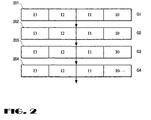
- Figure 2 shows schematically a 4-stage pipelined grouping logic circuit 109 in the 4-way superscalar processor of Figure 1.
- FIG. 1 An embodiment of the present invention is illustrated by the block diagram of Figure 1, which shows a central processing unit (CPU) 100 in an exemplary 4-way superscalar processor of the present invention.
- CPU central processing unit
- a 4-way superscalar processor fetches, dispatches, executes and retires up to four instructions per processor cycle.
- central processing unit 100 includes two arithmetic logic units 101 and 102, a load/store unit 103, which includes a 9-deep load buffer 104 and an 8-deep store buffer 105, a floating point adder 106, a floating point multiplier 107, and a floating point divider 108.
- a grouping logic circuit 109 dispatches up to four instructions per processor cycle.
- Completion unit 110 retires instructions upon completion.
- a register file (not shown), including numerous integer and float point registers, is provided with sufficient number of ports to prevent contention among functional units for access to this register file during operand fetch or result write-back.
- loads are non-blocking, i.e., CPU 100 continues to execute even though one or more dispatched load instructions have not complete.
- floating point adder 106 and floating point multiplier 107 each have a 4-stage pipeline.
- load/store unit 103 has a 2-stage pipeline.
- Floating point divider 108 which is not pipelined, requires more than one processor cycle per instruction.
- state of CPU 100 relevant to grouping logic 109 is summarized by a state variable S(t), which is defined below.
- S(t) the state of CPU 100 includes also other variables, such as those conventionally included in the processor status word.
- ALU 1 (t) and ALU 2 (t) are the states, at time t, of arithmetic logic units 101 and 102 respectively
- LS(t) and LB(t) are the states, at time t, of store buffer 105 and load buffer 104 respectively
- FA(t) , FM(t), and FDS(t) are the states, at time t, of floating point adder 106, floating point multiplier 107 and floating point divider 108 respectively.
- each functional unit can be represented by the source and destination registers specified in the instructions dispatched to the functional unit but not yet retired.
- ALU 1 ⁇ ALU 1 .rs1 ( t ), ALU 1 . rs2 ( t ), ALU 1 .rd ( t ) ⁇ where rs1(t), rs2(t) and rd(t) are respectively the first and second source registers, and the destination of registers of the instruction executing at time t in arithmetic logic unit 101.
- ALU 2 ⁇ ALU 2 . rs1 ( t ), ALU 2 . rs2 ( t ), ALU 2 . rd ( t ) ⁇
- State variable S(t) can be represented by a memory element, such as a register or a content addressable memory unit, at either a centralized location or in a distributed fashion.
- a memory element such as a register or a content addressable memory unit
- the portion of state S(t) associated with a given functional unit can be implemented with the control logic of the functional unit.
- a grouping logic circuit would determine from the current state, S(t) at time t, the next state S(t+1), which includes information necessary to dispatch the instructions of the next processor cycle at time t+1. For example, to avoid a read-after-write hazard, such a grouping circuit would exclude from the next state S(t+1) an instruction having an operand to be fetched from a register designated for storing a result of a yet incomplete instruction. As another example, such a grouping circuit would include in state S(t+1) no more than one floating point "add" instruction in each processor cycle, since only one floating point adder (i.e. floating point adder 106) is available.
- grouping logic circuit 109 is pipelined to derive, over ⁇ processor cycles, a future state S(t+ ⁇ ) based on the present state S(t).
- the future state S(t+ ⁇ ) determines the instruction group to dispatch at time t+ ⁇ .
- Pipelining grouping logic 109 is possible because, as demonstrated below, (i) the values of most state variables in the state S(t+ ⁇ ) can be estimated from corresponding values of state S(t) with sufficient accuracy, and (ii) for those state variables for which values can not be accurately predicted, it is relatively straightforward to provide for all possible outcomes of state S(t+ ⁇ ), or to use a conservative approach (i.e. not dispatching an instruction when such an instruction could have been dispatched) with a slight penalty on performance.
- the states FA, FM and LS at time t+1 can be derived from the corresponding state S(t) at time t, the immediately preceding processor cycle.
- state LB(t+1) at time t+1 cannot be determined from the immediately previous state LB(t) at time t with certainty.
- state LB(t+1) can only either remain the same, or reflect the movement of the pipeline by one stage, two possible approaches to determine state LB(t+1) can be used.
- a conservative approach would predict LB(t+1) to be the same as LB(t). Under this approach, when load buffer 104 is full, an instruction is not dispatched until the pipeline in load buffer 106 advances. An incorrect prediction, i.e.
- state S(t+1) of CPU 100 can be predicted from state S(t). Consequently, both the number of instructions and the types of instructions that can be dispatched at time t+1 (i.e. the instruction group at time t+1) based on predicted state S(t+1) can be derived, at time t, from state S(t), subject to additional handling based on the actual state S A (t+1) at time t+1.
- the above analysis can be can be extended to allow state S(t+ ⁇ ) at time t+ ⁇ to be derived from state S(t) at time t.
- the instruction group at time t+ ⁇ can be derived from time t, provided that, for each instruction group between time t and t+ ⁇ , all instruction from that instruction group must be dispatched before any instruction from a subsequent instruction group is allowed to be dispatched (i.e. no instruction group merging).
- the instructions are either fetched from an instruction cache or an instruction buffer.
- An instruction buffer is preferable in a system in which not all accesses (e.g. branch instructions) to the instruction cache are aligned, and multiple entry points in the basic blocks of a program are allowed.
- intra-group data dependency checking can begin. Because of the constraint against instruction group merging described above, i.e., all instructions in an instruction group must be dispatched before an instruction from a subsequent instruction group can be dispatched, intra-group dependency checking can be accomplished in a pipelined fashion. That is, intra-group dependency checking can span more than one processor cycle and all inter-group dependency checking can occur independently of inter-group dependency checking.
- An example of a four-stage pipeline 200 is shown in Figure 2. In Figure 2, at first stage 201, as soon as the instruction group is constituted, intra-group dependency checking is performed immediately. Thereafter, at stage 202, resource allocation within the instruction group can be determined. At stage 203, intergroup decisions, e.g.
- resource allocation decisions taking into consideration resource allocation in previous instruction groups are merged with the decisions at stages 201 and 202. For example, if the present instruction group includes an instruction designated for floating point divider 108, stage 203 would have determined at by this time if a previous instruction using floating point divider 108 would have completed by the time the present instruction group is due to be dispatched. Finally, at stage 204, non-deterministic conditions, e.g. the condition at store buffer 105, is considered. Dispatchable instructions are issued into CPU 100 at the end of stage 204.
Abstract
Description
- This invention relates to computer architecture. In particular, this invention relates to the design of an instruction unit in a superscalar processor.
- Parallelism is extensively exploited in modern computer designs. Among these designs are two distinct architectures which are known respectively as the very long instruction word (VLIW) architecture and the superscalar architecture. A superscalar processor is a computer which can dispatch one, two or more instructions simultaneously. Such a processor typically includes multiple functional units which can independently execute the dispatched instructions. In such a processor, a control logic circuit, which has come to be known as the "grouping logic" circuit, determines the instructions to dispatch (the "instruction group"), according to certain resource allocation and data dependency constraints. The task of the computer designer is to provide a grouping logic circuit which can dynamically evaluate such constraints to dispatch instruction groups which optimally use the available resources. A resource allocation constraint can be, for instance, in a computer with a single floating point multiplier unit, the constraint that no more than one floating point multiply instruction is to be dispatched for any given processor cycle. A processor cycle is the basic timing unit for a pipelined unit of the processor, typically the clock period of the CPU clock. An example of a data dependency constraint is the avoidance of a "read-after-write" hazard. This constraint prevents dispatching an instruction which requires an operand from a register which is the destination of an write instruction dispatched earlier, but yet to be unretired.
- A VLIW processor, unlike a superscalar processor, does not dynamically allocate system resources at run time. Rather, resource allocation and data dependency analysis are performed during program compilation. A VLIW processor decodes the long instruction word to provide the control information for operating the various independent functional units. The task of the compiler is to optimize performance of a program by generating a sequence of such instructions which, when decoded, efficiently exploit the program's inherent parallelism in the computer's parallel hardware. The hardware is given little control of instruction sequencing and dispatch.
- A VLIW computer, however, has a significant drawback in that its programs must be recompiled for each machine they run on. Such recompilation is required because the control information required by each machine is encoded in the instruction words. A superscalar computer, by contrast, is often designed to be able to run existing executable programs (i.e., "binaries"). In a superscalar computer, the instructions of an existing executable program are dispatched by the computer at run time according to the computer's particular resource availability and data integrity requirements. From a computer user's point of view, because existing binaries represent significant investments, the ability to acquire enhanced performance without the expense of purchasing new copies of binaries is a significant advantage.
- In the prior art, to determine the instructions that go into an instruction group of a given processor cycle, a superscalar computer performs the resource allocation and data dependency checking tasks in the immediately preceding processor cycle. Under this scheme, the computer designer must ensure that such resource allocation and data dependency checking tasks complete within their processor cycle. As the number of the functional units that can be independently run increases, the time required for performing such resource allocation and data dependency checking tasks grows more rapidly than linearly. Consequently, in a superscalar computer design, the ability to perform resource and data integrity analysis within a single processor cycle can become a factor that limits the performance gain of additional parallelism.
- The present invention provides a central processing unit which includes a grouping logic circuit for determining simultaneously dispatchable instructions in an processor cycle. The central processing unit of the present invention includes such a grouping logic circuit and a number of functional units, each adapted to execute one or more specified instructions dispatched by the grouping logic circuit. The grouping logic circuit includes a number of pipeline stages, such that resource allocation and data dependency checks can be performed over a number of processor cycles. The present invention therefore allows dispatching a large number of instruction simultaneously, while avoiding the complexity of the grouping logic circuit from becoming limiting the duration of the central processing unit's processor cycle.
- In one embodiment, the grouping logic circuit checks intra-group data dependency immediately upon receiving the instruction group. In that embodiment, all instruction in a group of instructions received in a first processor cycle are dispatched prior to dispatching any instruction of a second group of instructions received at an processor cycle subsequent to said first processor cycle.
- The present invention is better understood upon consideration of the detailed description below in conjunction with the accompanying drawings.
- Figure 1 is a block diagram of a
CPU 100, in an exemplary 4-way superscalar processor of the present invention. - Figure 2 shows schematically a 4-stage pipelined
grouping logic circuit 109 in the 4-way superscalar processor of Figure 1. - An embodiment of the present invention is illustrated by the block diagram of Figure 1, which shows a central processing unit (CPU) 100 in an exemplary 4-way superscalar processor of the present invention. A 4-way superscalar processor fetches, dispatches, executes and retires up to four instructions per processor cycle. As shown in Figure 1,
central processing unit 100 includes twoarithmetic logic units store unit 103, which includes a 9-deep load buffer 104 and an 8-deep store buffer 105, afloating point adder 106, afloating point multiplier 107, and afloating point divider 108. In this embodiment, agrouping logic circuit 109 dispatches up to four instructions per processor cycle.Completion unit 110 retires instructions upon completion. A register file (not shown), including numerous integer and float point registers, is provided with sufficient number of ports to prevent contention among functional units for access to this register file during operand fetch or result write-back. In this embodiment also, loads are non-blocking, i.e.,CPU 100 continues to execute even though one or more dispatched load instructions have not complete. When the data of the load instructions are returned from the main memory, these data can be placed in a pipeline for storage in a second-level cache. In this embodiment,floating point adder 106 andfloating point multiplier 107 each have a 4-stage pipeline. Similarly, load/store unit 103 has a 2-stage pipeline.Floating point divider 108, which is not pipelined, requires more than one processor cycle per instruction. - To simplify the discussion below, the state of
CPU 100 relevant togrouping logic 109 is summarized by a state variable S(t), which is defined below. Of course, the state ofCPU 100 includes also other variables, such as those conventionally included in the processor status word. Those skilled in the art would appreciate the use and implementation of processor states. Thus, the state S(t) at time t ofCPU 100 can be represented by:
ALU1(t) and ALU2(t) are the states, at time t, ofarithmetic logic units store buffer 105 andload buffer 104 respectively; FA(t) , FM(t), and FDS(t) are the states, at time t, offloating point adder 106,floating point multiplier 107 andfloating point divider 108 respectively. - At any given time, the state of each functional unit can be represented by the source and destination registers specified in the instructions dispatched to the functional unit but not yet retired. Thus,

arithmetic logic unit 101. - Similarly, the state of
arithmetic logic unit 102 can be defined as:
- For pipelined functional units, such as floating
point adder 106, the state is relatively more complex, consisting of the source and destination registers of the instructions in their respectively pipeline. Thus, for the pipelined units, i.e., load/store unit 103,load buffer 104,store buffer 105, floatingpoint adder 106, and floatingpoint multiplier 107, their respective states, at time t, LS(t), LB(t), SB(t), FA(t) and FM(t) can be represented by:


- Finally, floating
point divider 108's state FSD(t)

- State variable S(t) can be represented by a memory element, such as a register or a content addressable memory unit, at either a centralized location or in a distributed fashion. For example, in the distributed approach, the portion of state S(t) associated with a given functional unit can be implemented with the control logic of the functional unit.
- In the prior art, a grouping logic circuit would determine from the current state, S(t) at time t, the next state S(t+1), which includes information necessary to dispatch the instructions of the next processor cycle at
time t+ 1. For example, to avoid a read-after-write hazard, such a grouping circuit would exclude from the next state S(t+1) an instruction having an operand to be fetched from a register designated for storing a result of a yet incomplete instruction. As another example, such a grouping circuit would include in state S(t+1) no more than one floating point "add" instruction in each processor cycle, since only one floating point adder (i.e. floating point adder 106) is available. As discussed above, as complexity increases, the time required for propagating through the grouping logic circuit can become a critical path for the processor cycle. Thus, in accordance with the present invention,grouping logic circuit 109 is pipelined to derive, over τ processor cycles, a future state S(t+τ) based on the present state S(t). The future state S(t+τ) determines the instruction group to dispatch at time t+τ.Pipelining grouping logic 109 is possible because, as demonstrated below, (i) the values of most state variables in the state S(t+τ) can be estimated from corresponding values of state S(t) with sufficient accuracy, and (ii) for those state variables for which values can not be accurately predicted, it is relatively straightforward to provide for all possible outcomes of state S(t+τ), or to use a conservative approach (i.e. not dispatching an instruction when such an instruction could have been dispatched) with a slight penalty on performance. - The process for predicting state S(t+τ) is explained next. The following discussion will first show that most components of next state S(t+1) can be precisely determined from present state S(t), and the remaining components of state S(t) can be reasonably determined, provided that certain non-deterministic conditions are appropriately handled. By induction, it can therefore be shown that future state S(t+τ), where τ is greater than 1, can likewise be determined from state S(t).
- Since an instruction in floating
point adder 106 or floatingpoint multiplier 107 completes after four processor cycles and an instruction in load/store unit 103 completes after two processor cycles, the states FA, FM and LS at time t+1 can be derived from the corresponding state S(t) at time t, the immediately preceding processor cycle. In particular, the relationship governing the source and destination registers of each instruction executing in floatingpoint adder 106, floatingpoint multiplier 107 and load/store unit 103 between time t+1 and time t are:


- The state FSD(t+1) of floating
point divider 108, in which the time required to execute an instruction can exceed an processor cycle, is determined from state FSD(t) by:
point divider 108 is in its last stage can be determined from, for example, a hardware counter or a state register, which keep tracks of the number of processor cycles elapsed since the instruction in floatingpoint divider 108 began execution. - In
load buffer 104 andstore buffer 105, since the pending read or write operation at the head of each queue need not complete within one processor cycle, the state LB(t+1) at time t+1 cannot be determined from the immediately previous state LB(t) at time t with certainty. However, since state LB(t+1) can only either remain the same, or reflect the movement of the pipeline by one stage, two possible approaches to determine state LB(t+1) can be used. First, a conservative approach would predict LB(t+1) to be the same as LB(t). Under this approach, whenload buffer 104 is full, an instruction is not dispatched until the pipeline inload buffer 106 advances. An incorrect prediction, i.e. a load instruction completes during the processor cycle of time t, this conservative approach leads to a penalty of one processor cycle, since a load instruction could have been dispatched attime t+ 1. Alternatively, a more aggressive approach provides for both outcomes, i.e.load buffer 104 advances one stage, andload buffer 104 remains the same. Under this aggressive approach,grouping logic 109 is ready to dispatch a load instruction, such dispatch to be enabled by a control signal which indicates, attime t+ 1, whether a load instruction has in fact completed. This aggressive approach requires more a complex logic circuit than the conservative approach. - Thus, the skilled person would appreciate that state S(t+1) of
CPU 100 can be predicted from state S(t). Consequently, both the number of instructions and the types of instructions that can be dispatched at time t+1 (i.e. the instruction group at time t+1) based on predicted state S(t+1) can be derived, at time t, from state S(t), subject to additional handling based on the actual state SA(t+1) attime t+ 1. - The above analysis can be can be extended to allow state S(t+τ) at time t+τ to be derived from state S(t) at time t. The instruction group at time t+τ can be derived from time t, provided that, for each instruction group between time t and t+τ, all instruction from that instruction group must be dispatched before any instruction from a subsequent instruction group is allowed to be dispatched (i.e. no instruction group merging).
- Since instructions from different instruction groups are not merged, intra-group dependencies and inter-group dependencies can be checked in parallel. The instructions are either fetched from an instruction cache or an instruction buffer. An instruction buffer is preferable in a system in which not all accesses (e.g. branch instructions) to the instruction cache are aligned, and multiple entry points in the basic blocks of a program are allowed.
- Once four candidate instructions for an instruction group are identified, intra-group data dependency checking can begin. Because of the constraint against instruction group merging described above, i.e., all instructions in an instruction group must be dispatched before an instruction from a subsequent instruction group can be dispatched, intra-group dependency checking can be accomplished in a pipelined fashion. That is, intra-group dependency checking can span more than one processor cycle and all inter-group dependency checking can occur independently of inter-group dependency checking. For the purpose of intra-group dependency check, each instruction group can be represented by:

first stage 201, as soon as the instruction group is constituted, intra-group dependency checking is performed immediately. Thereafter, atstage 202, resource allocation within the instruction group can be determined. Atstage 203, intergroup decisions, e.g. resource allocation decisions taking into consideration resource allocation in previous instruction groups, are merged with the decisions atstages point divider 108,stage 203 would have determined at by this time if a previous instruction using floatingpoint divider 108 would have completed by the time the present instruction group is due to be dispatched. Finally, atstage 204, non-deterministic conditions, e.g. the condition atstore buffer 105, is considered. Dispatchable instructions are issued intoCPU 100 at the end ofstage 204. - The above detailed description is provided to illustrate the specific embodiments of the present invention and is not intended to be limiting. Numerous variations and modifications within the scope of the present invention are possible. The present invention is defined by the following claims.
Claims (9)
- A central processing unit, comprising:a plurality of functional units, each functional unit adapted to execute an instruction; anda grouping logic circuit, including a number of pipeline stages and receiving, at each processor cycle, a group of instructions, said grouping logic circuit dispatching each of said instructions to be executed by one of said functional units.
- A central processing unit as in Claim 1, wherein said grouping logic circuit checks data dependency among said group of instructions to determine whether said group of instructions can be dispatched simultaneously.
- A central processing unit as in Claim 1 or 2, wherein said grouping logic circuit checks for resource contention within said group of instructions.
- A central processing unit as in Claim 1, 2 or 3, wherein said grouping logic circuit checks data dependency of an instruction group at one processor cycle and a group of instruction received in a previous processor cycle.
- A central processing unit as in any preceding Claim, wherein the state of said central processing unit is represented in a register, said state including representation of destination registers of instructions in said group of instructions.
- A central processing unit as in any preceding Claim, wherein all instruction in a group of instructions received in a first processor cycle are dispatched prior to dispatching any instruction of a second group of instructions received at an processor cycle subsequent to said first processor cycle.
- A central processing unit as in any preceding Claim, wherein said functional units include a pipelined functional unit capable of receiving an instruction every processor cycle and completing said instruction at a subsequent processor cycle.
- A central processing unit as in any preceding Claim, wherein said functional units include a functional unit requiring multiple processor cycles to complete an instruction executed at said functional unit.
- A central processing unit as in any preceding Claim, wherein said grouping logic circuit derives a state vector for a group of instructions received at a first processor cycle based on a number of state vectors derived for groups of instructions received in a number of processor cycles immediately preceding said first processor cycle, said number of processor cycles being equal to said number of pipeline stages.
Applications Claiming Priority (2)
| Application Number | Priority Date | Filing Date | Title |
|---|---|---|---|
| US662582 | 1984-10-19 | ||
| US08/662,582 US5958042A (en) | 1996-06-11 | 1996-06-11 | Grouping logic circuit in a pipelined superscalar processor |
Publications (3)
| Publication Number | Publication Date |
|---|---|
| EP0813145A2 true EP0813145A2 (en) | 1997-12-17 |
| EP0813145A3 EP0813145A3 (en) | 1999-07-28 |
| EP0813145B1 EP0813145B1 (en) | 2005-10-05 |
Family
ID=24658307
Family Applications (1)
| Application Number | Title | Priority Date | Filing Date |
|---|---|---|---|
| EP97303831A Expired - Lifetime EP0813145B1 (en) | 1996-06-11 | 1997-06-04 | Pipelined instruction dispatch unit in a superscalar processor |
Country Status (5)
| Country | Link |
|---|---|
| US (3) | US5958042A (en) |
| EP (1) | EP0813145B1 (en) |
| JP (1) | JP3851707B2 (en) |
| KR (1) | KR100616722B1 (en) |
| DE (1) | DE69734303D1 (en) |
Cited By (4)
| Publication number | Priority date | Publication date | Assignee | Title |
|---|---|---|---|---|
| US10740126B2 (en) | 2013-03-15 | 2020-08-11 | Intel Corporation | Methods, systems and apparatus for supporting wide and efficient front-end operation with guest-architecture emulation |
| US11163720B2 (en) | 2006-04-12 | 2021-11-02 | Intel Corporation | Apparatus and method for processing an instruction matrix specifying parallel and dependent operations |
| US11204769B2 (en) | 2011-03-25 | 2021-12-21 | Intel Corporation | Memory fragments for supporting code block execution by using virtual cores instantiated by partitionable engines |
| US11656875B2 (en) | 2013-03-15 | 2023-05-23 | Intel Corporation | Method and system for instruction block to execution unit grouping |
Families Citing this family (24)
| Publication number | Priority date | Publication date | Assignee | Title |
|---|---|---|---|---|
| USRE38599E1 (en) * | 1996-06-11 | 2004-09-21 | Sun Microsystems, Inc. | Pipelined instruction dispatch unit in a superscalar processor |
| US5958042A (en) * | 1996-06-11 | 1999-09-28 | Sun Microsystems, Inc. | Grouping logic circuit in a pipelined superscalar processor |
| EP1050809A1 (en) * | 1999-05-03 | 2000-11-08 | STMicroelectronics SA | Computer instruction dependency |
| US6618802B1 (en) * | 1999-09-07 | 2003-09-09 | Hewlett-Packard Company, L.P. | Superscalar processing system and method for selectively stalling instructions within an issue group |
| US6651164B1 (en) * | 1999-10-14 | 2003-11-18 | Hewlett-Packard Development Company, L.P. | System and method for detecting an erroneous data hazard between instructions of an instruction group and resulting from a compiler grouping error |
| US6895497B2 (en) * | 2002-03-06 | 2005-05-17 | Hewlett-Packard Development Company, L.P. | Multidispatch CPU integrated circuit having virtualized and modular resources and adjustable dispatch priority |
| US7020765B2 (en) * | 2002-09-27 | 2006-03-28 | Lsi Logic Corporation | Marking queue for simultaneous execution of instructions in code block specified by conditional execution instruction |
| US20040128485A1 (en) * | 2002-12-27 | 2004-07-01 | Nelson Scott R. | Method for fusing instructions in a vector processor |
| US7191320B2 (en) * | 2003-02-11 | 2007-03-13 | Via Technologies, Inc. | Apparatus and method for performing a detached load operation in a pipeline microprocessor |
| US7237094B2 (en) * | 2004-10-14 | 2007-06-26 | International Business Machines Corporation | Instruction group formation and mechanism for SMT dispatch |
| JP4957729B2 (en) * | 2007-01-25 | 2012-06-20 | 日本電気株式会社 | Program parallelization method, program parallelization apparatus and program |
| KR101335001B1 (en) * | 2007-11-07 | 2013-12-02 | 삼성전자주식회사 | Processor and instruction scheduling method |
| JP5436033B2 (en) * | 2009-05-08 | 2014-03-05 | パナソニック株式会社 | Processor |
| EP2862062B1 (en) | 2012-06-15 | 2024-03-06 | Intel Corporation | A virtual load store queue having a dynamic dispatch window with a distributed structure |
| KR101993562B1 (en) * | 2012-06-15 | 2019-09-30 | 인텔 코포레이션 | An instruction definition to implement load store reordering and optimization |
| WO2013188306A1 (en) | 2012-06-15 | 2013-12-19 | Soft Machines, Inc. | Reordered speculative instruction sequences with a disambiguation-free out of order load store queue |
| CN107748673B (en) | 2012-06-15 | 2022-03-25 | 英特尔公司 | Processor and system including virtual load store queue |
| TWI646422B (en) | 2012-06-15 | 2019-01-01 | 英特爾股份有限公司 | Disambiguation-free out-of-order load/store queue methods in a processor, microprocessor, and non-transitory computer-readable storage medium |
| EP2862084A4 (en) | 2012-06-15 | 2016-11-30 | Soft Machines Inc | A method and system for implementing recovery from speculative forwarding miss-predictions/errors resulting from load store reordering and optimization |
| US9710278B2 (en) | 2014-09-30 | 2017-07-18 | International Business Machines Corporation | Optimizing grouping of instructions |
| US9971601B2 (en) | 2015-02-13 | 2018-05-15 | International Business Machines Corporation | Dynamic assignment across dispatch pipes of source ports to be used to obtain indication of physical registers |
| US9710281B2 (en) * | 2015-07-30 | 2017-07-18 | International Business Machines Corporation | Register comparison for operand store compare (OSC) prediction |
| US10089114B2 (en) | 2016-03-30 | 2018-10-02 | Qualcomm Incorporated | Multiple instruction issuance with parallel inter-group and intra-group picking |
| CN114327644B (en) * | 2022-03-16 | 2022-06-03 | 广东省新一代通信与网络创新研究院 | Method for realizing processor to predict memory access correlation |
Citations (3)
| Publication number | Priority date | Publication date | Assignee | Title |
|---|---|---|---|---|
| US5127093A (en) * | 1989-01-17 | 1992-06-30 | Cray Research Inc. | Computer look-ahead instruction issue control |
| EP0651323A1 (en) * | 1993-10-29 | 1995-05-03 | Advanced Micro Devices, Inc. | Microprocessors load/store functional units and data caches |
| US5497499A (en) * | 1992-03-31 | 1996-03-05 | Seiko Epson Corporation | Superscalar risc instruction scheduling |
Family Cites Families (16)
| Publication number | Priority date | Publication date | Assignee | Title |
|---|---|---|---|---|
| DE69123629T2 (en) * | 1990-05-04 | 1997-06-12 | Ibm | Machine architecture for scalar compound instruction set |
| US5295249A (en) * | 1990-05-04 | 1994-03-15 | International Business Machines Corporation | Compounding preprocessor for cache for identifying multiple instructions which may be executed in parallel |
| US5202975A (en) * | 1990-06-11 | 1993-04-13 | Supercomputer Systems Limited Partnership | Method for optimizing instruction scheduling for a processor having multiple functional resources |
| CA2038264C (en) * | 1990-06-26 | 1995-06-27 | Richard James Eickemeyer | In-memory preprocessor for a scalable compound instruction set machine processor |
| US5193167A (en) * | 1990-06-29 | 1993-03-09 | Digital Equipment Corporation | Ensuring data integrity by locked-load and conditional-store operations in a multiprocessor system |
| JP2535252B2 (en) * | 1990-10-17 | 1996-09-18 | 三菱電機株式会社 | Parallel processor |
| GB9027853D0 (en) * | 1990-12-21 | 1991-02-13 | Inmos Ltd | Multiple instruction issue |
| US5488729A (en) * | 1991-05-15 | 1996-01-30 | Ross Technology, Inc. | Central processing unit architecture with symmetric instruction scheduling to achieve multiple instruction launch and execution |
| GB9123271D0 (en) * | 1991-11-02 | 1991-12-18 | Int Computers Ltd | Data processing system |
| JP3544214B2 (en) * | 1992-04-29 | 2004-07-21 | サン・マイクロシステムズ・インコーポレイテッド | Method and system for monitoring processor status |
| KR100309566B1 (en) * | 1992-04-29 | 2001-12-15 | 리패치 | Method and apparatus for grouping multiple instructions, issuing grouped instructions concurrently, and executing grouped instructions in a pipeline processor |
| US5546593A (en) * | 1992-05-18 | 1996-08-13 | Matsushita Electric Industrial Co., Ltd. | Multistream instruction processor able to reduce interlocks by having a wait state for an instruction stream |
| US5627984A (en) * | 1993-03-31 | 1997-05-06 | Intel Corporation | Apparatus and method for entry allocation for a buffer resource utilizing an internal two cycle pipeline |
| DE69422780T2 (en) * | 1993-11-05 | 2000-08-17 | Intergraph Corp | Superscalar computer architecture with software scheduling |
| US5555432A (en) * | 1994-08-19 | 1996-09-10 | Intel Corporation | Circuit and method for scheduling instructions by predicting future availability of resources required for execution |
| US5958042A (en) | 1996-06-11 | 1999-09-28 | Sun Microsystems, Inc. | Grouping logic circuit in a pipelined superscalar processor |
-
1996
- 1996-06-11 US US08/662,582 patent/US5958042A/en not_active Expired - Lifetime
-
1997
- 1997-06-04 DE DE69734303T patent/DE69734303D1/en not_active Expired - Lifetime
- 1997-06-04 EP EP97303831A patent/EP0813145B1/en not_active Expired - Lifetime
- 1997-06-10 JP JP15173897A patent/JP3851707B2/en not_active Expired - Lifetime
- 1997-06-11 KR KR1019970023946A patent/KR100616722B1/en not_active IP Right Cessation
-
1999
- 1999-08-02 US US09/583,097 patent/US7430653B1/en not_active Expired - Fee Related
-
2000
- 2000-07-25 US US09/625,268 patent/US6349381B1/en not_active Ceased
Patent Citations (3)
| Publication number | Priority date | Publication date | Assignee | Title |
|---|---|---|---|---|
| US5127093A (en) * | 1989-01-17 | 1992-06-30 | Cray Research Inc. | Computer look-ahead instruction issue control |
| US5497499A (en) * | 1992-03-31 | 1996-03-05 | Seiko Epson Corporation | Superscalar risc instruction scheduling |
| EP0651323A1 (en) * | 1993-10-29 | 1995-05-03 | Advanced Micro Devices, Inc. | Microprocessors load/store functional units and data caches |
Non-Patent Citations (2)
| Title |
|---|
| POPESCU V ET AL: "THE METAFLOW ARCHITECTURE" IEEE MICRO, vol. 11, no. 3, 1 June 1991, pages 10-13, 63 - 73, XP000237231 * |
| SWEETMAN D: "SUPERSCALAR OR SUPERPIPELINED OR JUST HYPE?" NEW ELECTRONICS, vol. 24, no. 11, 1 December 1991, pages 16-18, XP000310175 * |
Cited By (4)
| Publication number | Priority date | Publication date | Assignee | Title |
|---|---|---|---|---|
| US11163720B2 (en) | 2006-04-12 | 2021-11-02 | Intel Corporation | Apparatus and method for processing an instruction matrix specifying parallel and dependent operations |
| US11204769B2 (en) | 2011-03-25 | 2021-12-21 | Intel Corporation | Memory fragments for supporting code block execution by using virtual cores instantiated by partitionable engines |
| US10740126B2 (en) | 2013-03-15 | 2020-08-11 | Intel Corporation | Methods, systems and apparatus for supporting wide and efficient front-end operation with guest-architecture emulation |
| US11656875B2 (en) | 2013-03-15 | 2023-05-23 | Intel Corporation | Method and system for instruction block to execution unit grouping |
Also Published As
| Publication number | Publication date |
|---|---|
| JPH1097424A (en) | 1998-04-14 |
| EP0813145A3 (en) | 1999-07-28 |
| US7430653B1 (en) | 2008-09-30 |
| EP0813145B1 (en) | 2005-10-05 |
| KR980004028A (en) | 1998-03-30 |
| DE69734303D1 (en) | 2005-11-10 |
| KR100616722B1 (en) | 2006-12-07 |
| JP3851707B2 (en) | 2006-11-29 |
| US6349381B1 (en) | 2002-02-19 |
| US5958042A (en) | 1999-09-28 |
Similar Documents
| Publication | Publication Date | Title |
|---|---|---|
| US5958042A (en) | Grouping logic circuit in a pipelined superscalar processor | |
| EP0411747B1 (en) | Multiple instruction decoder | |
| US6247115B1 (en) | Non-stalling circular counterflow pipeline processor with reorder buffer | |
| US5913925A (en) | Method and system for constructing a program including out-of-order threads and processor and method for executing threads out-of-order | |
| US6212542B1 (en) | Method and system for executing a program within a multiscalar processor by processing linked thread descriptors | |
| US5694565A (en) | Method and device for early deallocation of resources during load/store multiple operations to allow simultaneous dispatch/execution of subsequent instructions | |
| WO1985000453A1 (en) | Data processing system | |
| GB2321543A (en) | Constructing a program including a navigation instruction | |
| USRE38599E1 (en) | Pipelined instruction dispatch unit in a superscalar processor | |
| US5875326A (en) | Data processing system and method for completing out-of-order instructions | |
| EP0778519B1 (en) | Multiple instruction dispatch system for pipelined microprocessor without branch breaks | |
| US11481223B2 (en) | Reducing operations of sum-of-multiply-accumulate (SOMAC) instructions | |
| GB2321544A (en) | Concurrently executing multiple threads containing data dependent instructions | |
| US5850563A (en) | Processor and method for out-of-order completion of floating-point operations during load/store multiple operations | |
| US5713012A (en) | Microprocessor | |
| JPH10187464A (en) | Method and system for generating multiscalar program | |
| Rau et al. | Instruction-level parallelism | |
| US6490653B1 (en) | Method and system for optimally issuing dependent instructions based on speculative L2 cache hit in a data processing system | |
| Brehob et al. | Beyond RISC–The Post-RISC Architecture | |
| Burns et al. | Modelling of superscalar processor architectures with design/CPN | |
| Küçük et al. | Instruction Scheduling in Microprocessors | |
| Fernandes et al. | A study of associative dispatch in superscalar processors | |
| Page et al. | Advanced Processor Design | |
| KR19980037092A (en) | Pipeline Structure with Dual Function Validation Flow | |
| KR19980035724A (en) | Pipeline Structure with Functional Verification Flow and Its Pipelining Method |
Legal Events
| Date | Code | Title | Description |
|---|---|---|---|
| PUAI | Public reference made under article 153(3) epc to a published international application that has entered the european phase |
Free format text: ORIGINAL CODE: 0009012 |
|
| AK | Designated contracting states |
Kind code of ref document: A2 Designated state(s): DE GB NL SE |
|
| AX | Request for extension of the european patent |
Free format text: AL;LT;LV;SI |
|
| PUAL | Search report despatched |
Free format text: ORIGINAL CODE: 0009013 |
|
| AK | Designated contracting states |
Kind code of ref document: A3 Designated state(s): AT BE CH DE DK ES FI FR GB GR IE IT LI LU MC NL PT SE |
|
| AX | Request for extension of the european patent |
Free format text: AL;LT;LV;SI |
|
| 17P | Request for examination filed |
Effective date: 20000106 |
|
| AKX | Designation fees paid |
Free format text: DE GB NL SE |
|
| 17Q | First examination report despatched |
Effective date: 20030603 |
|
| GRAP | Despatch of communication of intention to grant a patent |
Free format text: ORIGINAL CODE: EPIDOSNIGR1 |
|
| GRAS | Grant fee paid |
Free format text: ORIGINAL CODE: EPIDOSNIGR3 |
|
| GRAA | (expected) grant |
Free format text: ORIGINAL CODE: 0009210 |
|
| AK | Designated contracting states |
Kind code of ref document: B1 Designated state(s): DE GB NL SE |
|
| PG25 | Lapsed in a contracting state [announced via postgrant information from national office to epo] |
Ref country code: NL Free format text: LAPSE BECAUSE OF FAILURE TO SUBMIT A TRANSLATION OF THE DESCRIPTION OR TO PAY THE FEE WITHIN THE PRESCRIBED TIME-LIMIT Effective date: 20051005 |
|
| REG | Reference to a national code |
Ref country code: GB Ref legal event code: FG4D |
|
| REF | Corresponds to: |
Ref document number: 69734303 Country of ref document: DE Date of ref document: 20051110 Kind code of ref document: P |
|
| PG25 | Lapsed in a contracting state [announced via postgrant information from national office to epo] |
Ref country code: SE Free format text: LAPSE BECAUSE OF FAILURE TO SUBMIT A TRANSLATION OF THE DESCRIPTION OR TO PAY THE FEE WITHIN THE PRESCRIBED TIME-LIMIT Effective date: 20060105 |
|
| PG25 | Lapsed in a contracting state [announced via postgrant information from national office to epo] |
Ref country code: DE Free format text: LAPSE BECAUSE OF FAILURE TO SUBMIT A TRANSLATION OF THE DESCRIPTION OR TO PAY THE FEE WITHIN THE PRESCRIBED TIME-LIMIT Effective date: 20060106 |
|
| NLV1 | Nl: lapsed or annulled due to failure to fulfill the requirements of art. 29p and 29m of the patents act | ||
| PLBE | No opposition filed within time limit |
Free format text: ORIGINAL CODE: 0009261 |
|
| STAA | Information on the status of an ep patent application or granted ep patent |
Free format text: STATUS: NO OPPOSITION FILED WITHIN TIME LIMIT |
|
| 26N | No opposition filed |
Effective date: 20060706 |
|
| PGFP | Annual fee paid to national office [announced via postgrant information from national office to epo] |
Ref country code: GB Payment date: 20160601 Year of fee payment: 20 |
|
| REG | Reference to a national code |
Ref country code: GB Ref legal event code: PE20 Expiry date: 20170603 |
|
| PG25 | Lapsed in a contracting state [announced via postgrant information from national office to epo] |
Ref country code: GB Free format text: LAPSE BECAUSE OF EXPIRATION OF PROTECTION Effective date: 20170603 |