EP0821506A1 - Multiplex transmitter for micro-frame - Google Patents
Multiplex transmitter for micro-frame Download PDFInfo
- Publication number
- EP0821506A1 EP0821506A1 EP96942630A EP96942630A EP0821506A1 EP 0821506 A1 EP0821506 A1 EP 0821506A1 EP 96942630 A EP96942630 A EP 96942630A EP 96942630 A EP96942630 A EP 96942630A EP 0821506 A1 EP0821506 A1 EP 0821506A1
- Authority
- EP
- European Patent Office
- Prior art keywords
- micro
- frames
- multiplex
- atm cell
- extracting
- Prior art date
- Legal status (The legal status is an assumption and is not a legal conclusion. Google has not performed a legal analysis and makes no representation as to the accuracy of the status listed.)
- Granted
Links
Images


Classifications
-
- H—ELECTRICITY
- H04—ELECTRIC COMMUNICATION TECHNIQUE
- H04Q—SELECTING
- H04Q11/00—Selecting arrangements for multiplex systems
- H04Q11/04—Selecting arrangements for multiplex systems for time-division multiplexing
- H04Q11/0428—Integrated services digital network, i.e. systems for transmission of different types of digitised signals, e.g. speech, data, telecentral, television signals
- H04Q11/0478—Provisions for broadband connections
-
- H—ELECTRICITY
- H04—ELECTRIC COMMUNICATION TECHNIQUE
- H04L—TRANSMISSION OF DIGITAL INFORMATION, e.g. TELEGRAPHIC COMMUNICATION
- H04L12/00—Data switching networks
- H04L12/28—Data switching networks characterised by path configuration, e.g. LAN [Local Area Networks] or WAN [Wide Area Networks]
-
- H—ELECTRICITY
- H04—ELECTRIC COMMUNICATION TECHNIQUE
- H04L—TRANSMISSION OF DIGITAL INFORMATION, e.g. TELEGRAPHIC COMMUNICATION
- H04L12/00—Data switching networks
- H04L12/54—Store-and-forward switching systems
- H04L12/56—Packet switching systems
- H04L12/5601—Transfer mode dependent, e.g. ATM
- H04L2012/5638—Services, e.g. multimedia, GOS, QOS
- H04L2012/5646—Cell characteristics, e.g. loss, delay, jitter, sequence integrity
- H04L2012/5649—Cell delay or jitter
-
- H—ELECTRICITY
- H04—ELECTRIC COMMUNICATION TECHNIQUE
- H04L—TRANSMISSION OF DIGITAL INFORMATION, e.g. TELEGRAPHIC COMMUNICATION
- H04L12/00—Data switching networks
- H04L12/54—Store-and-forward switching systems
- H04L12/56—Packet switching systems
- H04L12/5601—Transfer mode dependent, e.g. ATM
- H04L2012/5638—Services, e.g. multimedia, GOS, QOS
- H04L2012/5646—Cell characteristics, e.g. loss, delay, jitter, sequence integrity
- H04L2012/5652—Cell construction, e.g. including header, packetisation, depacketisation, assembly, reassembly
- H04L2012/566—Cell construction, e.g. including header, packetisation, depacketisation, assembly, reassembly using the ATM layer
- H04L2012/5661—Minicells
-
- H—ELECTRICITY
- H04—ELECTRIC COMMUNICATION TECHNIQUE
- H04L—TRANSMISSION OF DIGITAL INFORMATION, e.g. TELEGRAPHIC COMMUNICATION
- H04L12/00—Data switching networks
- H04L12/54—Store-and-forward switching systems
- H04L12/56—Packet switching systems
- H04L12/5601—Transfer mode dependent, e.g. ATM
- H04L2012/5672—Multiplexing, e.g. coding, scrambling
-
- H—ELECTRICITY
- H04—ELECTRIC COMMUNICATION TECHNIQUE
- H04L—TRANSMISSION OF DIGITAL INFORMATION, e.g. TELEGRAPHIC COMMUNICATION
- H04L12/00—Data switching networks
- H04L12/54—Store-and-forward switching systems
- H04L12/56—Packet switching systems
- H04L12/5601—Transfer mode dependent, e.g. ATM
- H04L2012/5678—Traffic aspects, e.g. arbitration, load balancing, smoothing, buffer management
- H04L2012/5679—Arbitration or scheduling
-
- H—ELECTRICITY
- H04—ELECTRIC COMMUNICATION TECHNIQUE
- H04L—TRANSMISSION OF DIGITAL INFORMATION, e.g. TELEGRAPHIC COMMUNICATION
- H04L12/00—Data switching networks
- H04L12/54—Store-and-forward switching systems
- H04L12/56—Packet switching systems
- H04L12/5601—Transfer mode dependent, e.g. ATM
- H04L2012/5678—Traffic aspects, e.g. arbitration, load balancing, smoothing, buffer management
- H04L2012/5681—Buffer or queue management
Definitions
- the present invention relates to a system configuration for loading a standard ATM cell with connections in the form of multiple low rate micro-frames in accordance with predetermined format in ATM (asynchronous transfer mode) transmission.
- Methods for loading a standard ATM cell with multiplexed connections in the form of micro-frames including data shorter than the standard ATM cell are variously proposed, and one of them is disclosed, for example, in Japanese patent application No. 7-266039, "Short cell multiplexed ATM transmission system and transmission method", which was filed by the assignee of the present invention.
- the inventors of the present invention do not know any concrete configuration designed for multiplexing the micro-frames, and for carrying out its control and fast processing thereof in a multiplex transmitter that performs multiplexing of the micro-frames.
- the object of the present invention is to provide a concrete configuration of a high speed multiplexed transmitter for loading standard ATM cells with a plurality of connections in the form of micro-frames including data shorter than the standard ATM cell.
- Another object of the present invention is to achieve effective multiplex transmission processing by incorporating two buffers, a buffer for deciding micro-frames to be multiplexed and a transmission queuing buffer, into a single queuing buffer.
- Still another object of the present invention is to achieve quality management of micro-frame connections having multiple qualities concerning a tolerable multiplexing wait time or a micro-frame cancellation ratio, and to implement multiplex transmission processing at high efficiency.
- a multiplex transmitter for performing multiplex transmission by loading a standard ATM cell with multiplexed connections composed of micro-frames each including data shorter than the standard ATM cell, the multiplex transmitter comprising:
- a multiplex transmitter for performing multiplex transmission by loading a standard ATM cell with multiplexed connections composed of micro-frames each including data shorter than the standard ATM cell, the multiplex transmitter comprising:
- the distributor may distribute the input micro-frames to the buffers having different multiplexing schemes in accordance with predetermined service conditions.
- the multiplexing processor may determine extracting order from the buffers in accordance with the service conditions, may extract the micro-frames, and may select the multiplexing scheme in accordance with the service conditions.
- a multiplex transmitter for performing multiplex transmission by loading a standard ATM cell with multiplexed connections composed of micro-frames each including data shorter than the standard ATM cell, the multiplex transmitter comprising:
- a multiplex transmitter for performing multiplex transmission by loading a standard ATM cell with multiplexed connections composed of micro-frames each including data shorter than the standard ATM cell, the multiplex transmitter comprising:
- the multiplex transmitter may distribute the input micro-frames to the buffers having different multiplexing schemes or canceling times of the micro-frames in accordance with predetermined service conditions.
- the multiplexing processor may determine extracting order from the buffers in accordance with the service conditions, may extract the micro-frames, and may select the multiplexing scheme in accordance with the service conditions.
- the extracting portion may perform extracting control not only of the transmission queuing buffer which stores the ATM cell onto which the multiplexing has been carried out, but also of the transmission queuing buffer which stores the ATM cell onto which no multiplexing has been carried out.
- the extracting portion may perform extracting control not only of the buffers which store multiplexed micro-frames, but also of a transmission queuing buffer which stores ATM cell onto which no multiplexing has been carried out.
- Fig. 1A illustrates a standard ATM cell.
- the standard ATM cell has a fixed length of 53 bytes including a 5-byte header and a 48-byte payload (information field).
- the present invention multiplexes micro-frames including data shorter than the standard ATM cell.
- the micro-frame can be variable or fixed in its length. Furthermore, it can overlap two standard ATM cells as in pattern (3), or it cannot fill out the standard ATM cell as in pattern (2). In this case, dummy bits are filled to be transmitted.
- the micro-frame may be longer than the standard ATM cell.
- FIGs. 2A and 2B are block diagrams showing an embodiment 1 of a multiplex transmitter 201 for transmitting multiplexed cell in accordance with the present invention.
- Fig. 3 illustrate the logic of extracting circuits 206 used in the multiplex transmitter 201
- Fig. 4 shows a configuration of a receiving demultiplexer 401.
- micro-frames that is, data connections 1-n, which are input to the multiplex transmitter 201 can be fixed or variable in length, or the same connection may be a link of fixed and variable lengths.
- the maximum number k of the micro-frames multiplexed into a single standard ATM cell is fixed. The maximum multiplexed number k is determined depending on a system environment and service conditions.
- the transmission rate of the multiplex transmitter 201 is much higher than that of the input connections, and an interface 203 has a conflict control function between the input connections.
- all the input micro-frames can be processed in accordance with the input sequence attached thereto between the interface 203 and distributor 204, or between the interface 203 and multiplex queuing buffer 205.
- the input micro-frames are fed to the distributor 204 through the interface 203 according to the input order.
- the distributor 204 distributes the input micro-frames using input distributing information.
- the present transmitter presumes to be basically used with a switching system (not shown) or the like which can identify the service types of the connections. Accordingly, the distributing information is generally sent from the switching system or the like.
- the distributing information accords with the service condition of each connection or micro-frame.
- the service condition such as a cancellation tolerable time, a micro-frame cancellation ratio, or a multiplexing scheme like a maximum number k of multiplexed micro-frames can be separately assigned to a multiplexing processor 207 and cell cancellation monitor circuit 208 to distribute each micro-frame or connection.
- the service condition is determined for each connection.
- the distributing information should be identified for each connection.
- the micro-frame itself can have service information serving as the distributing information with predetermined format so that the distributor 204 can distribute in accordance with that information.
- the distributor 204 selects one of multiplex queuing buffers 205 for each micro-frame to be stored, in accordance with the distributing information.
- extracting circuits 206 have multiplexing wait times T1-1 - T1-m, and cell cancellation monitor circuits 208 have cell cancellation tolerable times T2-1 - T2-m, which are set in advance as fixed parameters of the system, where T1 and T2 are values determined in accordance with the system environment and service conditions.
- each extracting circuit 206 keeps a constant monitoring over the corresponding multiplex queuing buffer 205 (S300).
- S302 When the micro-frame is input to the multiplex queuing buffer 205, it starts processing: it checks whether a timer has been set (S302), and starts the timer if it has not yet been set (S304). If the timer has been set, it checks whether the number of micro-frames stored in the multiplex queuing buffer 205 equals the predetermined number k (S306). If the number is less than k, the extracting circuit 206 returns to the monitoring state (S300).
- each extracting circuit 206 extracts the input micro-frames if their number reaches the preset number before the dwell time of the first input micro-frame counted from the end of the vacant state of the buffer exceeds time T1, and transfer the micro-frames to the corresponding multiplexing processor 207. In addition, unless the number of input micro-frames exceeds the preset number when the dwell time passes T1, the extracting circuit 206 transfers the entire input micro-frames to the multiplexing processor 207.
- the multiplexing processor 207 carries out multiplex processing of the received micro-frames in accordance with the predetermined format to transform them into the standard ATM form, and stores it in each transmission queuing buffer 209.
- An extraction selector 210 extracts from the transmission queuing buffers 209 the ATM cells, which have undergone the multiplex processing, in accordance with the logic of the extraction information input thereto, and transfers them to a sender 211.
- Each cell cancellation monitor circuit 208 monitors the corresponding transmission queuing buffer 209 ceaselessly, and relinquishes the cells that dwell there over time T2.
- the sender 211 outputs the cells extracted from the second buffers 209 at timings in accordance with output schemes.
- the data thus multiplexed into standard ATM cells and transferred are demultiplexed to the original micro-frames at the receiving side.
- the configuration of a receiving demultiplexer 401 is shown in Fig. 4.
- the receiving demultiplexer 401 is a unit for extracting micro-frames from the received cells.
- the received input cells are temporarily stored in a buffer 403, and a demultiplexing processor 404 carries out the demultiplex processing of the micro-frames in a manner corresponding to the multiplex processing in the transmitting side.
- the connection identification information of the micro-frames are present in each frame. It is necessary for this unit to possess the distributing information to perform the connection demultiplexing physically in this unit. In this case, the distributing information must be sent from the switching system as in the transmitting side, or added to the standard ATM cell in a predetermined format as identification information of the service conditions. In the former case, between the transmitting and receiving switching systems, a function for identifying negotiation processing of the service conditions of the multiplexed cells must be added to each connection of the micro-frames for distributing them.
- the receiving end Since the transmitting side carries out the cell cancellation to maintain the efficiency and quality of channels, the receiving end must perform the interpolation of the omitted cells, which is implemented by an interpolator 406.
- the function can be placed in a unit other than the receiving demultiplexer 401.
- the demultiplexed outputs for respective output connections are produced through an interface 407.
- Figs. 5A and 5B are block diagrams showing the configuration of the embodiment 2 of a multiplex transmitter 501 in accordance with the present invention.
- Fig. 6 is a flowchart illustrating an example of the buffer selection logic.
- the embodiment 1 of the multiplex transmitter 201 uses the fixed number k as a criterion for extracting the micro-frames from the buffers
- the embodiment 2 of the multiplex transmitter 501 differs from that in that it employs loadable data lengths onto the next cells, which are provided from multiplexing processors 507.
- each of the multiplexing processors 507 in the embodiment 2 of the multiplex transmitter 501 can notify of the data length x of the next cell to be multiplexed into the standard ATM cell.
- extracting circuits 506 and multiplexing processors 507 in the multiplex transmitter 501 differ in operation from their counterparts of the embodiment 1 as shown in Figs. 2A and 2B. Since the operation of the other circuits is the same as that of the circuits in the multiplex transmitter 201 of Figs. 2A and 2B, the description thereof is omitted here. The operation of the two sets of circuits 506 and 507 will now be described.
- the extracting circuits 506 have tolerable multiplexing wait times T1-1 - T1-m
- cell cancellation monitor circuits 508 have cell cancellation tolerable times T2-1 - T2-m, which are set in advance as in the circuits of the embodiment 1 as shown in Figs. 2A and 2B.
- the times T1 and T2 are values determined in accordance with the system environment and service conditions.
- the flowchart in Fig. 6 shows the extraction processing in the extracting circuits 506, which is similar to that of the extracting circuits 206 in Fig. 3 except for the step (S606) of checking the micro-frames stored in multiplex queuing buffers 505.
- each extracting circuit 506 checks the total length of the input micro-frames using the loadable length (x) sent from the corresponding multiplexing processor 507 instead of the fixed number (k) of the micro-frames as shown in the flowchart of Fig. 3.
- each extracting circuit 506 extracts the input micro-frames if their total length reaches the loadable length before the dwell time of the first input micro-frame counted from the end of the vacant state of the buffer exceeds the time T1, and transfers the micro-frames to the corresponding multiplexing processor 507. In addition, unless the total length of the input micro-frames exceeds the loadable length when the dwell time passes T1, the extracting circuit 506 transfers the entire input micro-frames to the multiplexing processor 507.
- Each multiplexing processor 507 carries out multiplex processing of the received micro-frames in accordance with the predetermined format to transform them into the standard ATM form, and stores it in each transmission queuing buffer 509. Besides, it computes the data length of the micro-frames loadable onto the next ATM cell, and notifies the extracting circuit of it.
- the length of the data loadable onto the next ATM cell is computed considering an overlapped portion in the case where one of the micro-frames is multiplexed across the current and next ATM cells as in the pattern (3) shown in Fig. 1B, in which case the length of the data loadable onto the next ATM cell surely reduces.
- the length of the data loadable onto the next ATM cell is computed and sent to the extracting circuit 506.
- the notification from the multiplexing processor 507 is unnecessary.
- FIG. 7 is a block diagram showing the configuration of an embodiment 3 of a multiplex transmitter 701 in accordance with the present invention.
- Fig. 8 is a diagram illustrating processing schedules of a processing timing controller 710
- Fig. 9 is a flowchart showing the operation of an extracting circuit 706
- Fig. 10 is a flowchart showing an example of the buffer selection logic
- Figs. 11A and 11B are flowcharts showing the processing logic of a multiplexing processor 707.
- the multiplex transmitter can handle a micro-frame which overlaps more than one standard ATM cells. It can also handle the micro-frames which do not overlapped. It is a matter of choice whether the overlapped cell is allowed or not.
- Fig. 7 shows the configuration of the multiplex transmitter 701.
- the reference numeral 703 designates an interface circuit that inputs the data connections 1-n in the form of a micro-frame structure.
- the reference numeral 704 designates a distributor that distributes the micro-frames to m buffers 705 in accordance with the service condition of each micro-frame.
- the reference numeral 706 designates an extracting circuit that extracts from the m buffers 705 micro-frames to be subjected to the multiplex processing at every processing interval.
- the reference numeral 707 designates a multiplexing processor that multiplexes the micro-frames extracted by the extracting circuit 706 onto the standard ATM cell or standard ATM cells in accordance with a predetermined scheme or a designated scheme, and 708 designates a sender that sends the processed cell or the idle cell to an output channel 709 in accordance with the standard of the output channel.
- the micro-frames in the input data connections 1-n can have a fixed or variable length depending on the connections, or a combination of the fixed and variable lengths can be allowed for the same channel.
- This embodiment will be described on the assumption that the maximum number of micro-frames which can be multiplexed onto a single standard ATM cell is a fixed number k.
- the maximum multiplexing number k which is determined depending on the system environment and service conditions, is decided as one of the service conditions for each connection or micro-frame.
- the service condition is determined for each connection.
- the distributing information should be identified connection by connection.
- the micro-frame itself can each have service information as the distributing information with predetermined format so that the distributor 704 can distribute in accordance with that information.
- the distributor 704 selects one of buffers 705 for each micro-frame to be stored, in accordance with the distributing information.
- the distributor 704 distributes the input micro-frames in accordance with the distributing information.
- the distributing information agrees with the service condition of each connection or micro-frame.
- the distribution can be achieved for each micro-frame or connection by separately assigning in the respective buffers the cancellation tolerable time and micro-frame cancellation ratio as the service conditions, and by notifying the extracting circuit 706 of the extracting procedure that satisfies each service condition.
- a cell cancellation monitor circuit 711 manages the input time of each micro-frame to the buffer. This is performed by attaching the input time information to each micro-frame, or by recording it in the memory corresponding to each input micro-frame.
- the cell cancellation monitor circuit 711 keeps comparing the input times of the micro-frames input to the m buffers 705 with the cancellation times T1-1 - T1-m determined in advance as fixed system parameters, and cancels the micro-frames which dwell in the buffers for more than cancellation tolerable times T1-1 - T1-m that are values determined depending on the system environment and service conditions.
- the transmission rate of the multiplex transmitter is much higher than that of the input connections, and the interface circuit 703 has a conflict control function between the input connections.
- all the input micro-frames can be processed in accordance with the input sequence by the interface circuit 703, distributor 704 and the multiplex queuing buffer 205.
- a processing timing controller 710 basically provides the respective circuits with processing timings to control the conflicts among the circuits.
- Fig. 8 illustrates the processing schedules of the circuits controlled by the processing timing controller 710. It is a matter of choice whether the cell output is carried out in the form of direct transfer of each standard ATM cell, or in the form of batch transfer of multiple cells generated like scrambled frames. The cell transfer timings of Fig. 8 is the case of the direct transfer.
- the extracting, multiplexing and transfer processings of the extracting circuit 706, multiplexing processor 707 and sender 708 can be achieved either in sequence or in parallel.
- the sequential processing can be employed only when the time taken for completing the extracting processing of the entire micro-frames to be multiplexed is at least less than or equal to the time taken from the beginning to the end of outputting one ATM cell.
- the parallel processing of the extracting, multiplexing and transfer processings enables the time taken for completing the extraction of the micro-frames to be postponed after the beginning of the multiplexed cell transfer.
- pattern 1 refers to the parallel processing of the extracting, multiplexing and transfer processings
- patter 2 refers to the sequential processings thereof.
- the extracting circuit 706 extracts the micro-frames from the buffers 1-m, and transfers the micro-frames to be multiplexed to the multiplexing processor 707.
- the extracting processing from the buffers 705 by the extracting circuit 706 will now be described with reference to the time chart of Fig. 8 and the flowchart of Fig. 9.
- the processings designated by pattern 1 and pattern 2 are carried out only for the pattern 1 and pattern 2, respectively.
- the fundamental extracting processing is to select the buffer i from which the micro-frames are to be extracted (S903), and to continue micro-frame collecting processing until the number of extracted micro-frames reaches. the multiplexed number k (S909) or until time-out (S913).
- the micro-frames are extracted one by one, and transferred to the multiplexing processor 707 (S911 and S927).
- notification 1 if no micro-frame is collected (NO at S915) until the end of the processing time (YES at S913), notification 1 (no micro-frame is present) is sent to the multiplexing processor 707 (S929).
- notification 2 if there is at least one micro-frame at the time-out, or k micro-frames are collected, notification 2 (micro-frame is present) is transferred together with the entire micro-frames collected (S917).
- the buffer i in Fig. 9 is fixed.
- Fig. 10 illustrates an example of the buffer selection logic.
- the processing illustrated in Fig. 10 is an example of the foregoing method 1 extracting each cell cyclically from the first to m-th buffer.
- the buffer selection logic is started with the value i of the buffer being set at its initial value 1 at the beginning of the decision processing. If there is any micro-frame in the buffer i (YES at S1003), the processing proceeds to the next step without changing the number i of the selected buffer. If there is not any micro-frame in the buffer (NO at S1003), the processing proceeds to the next step after selecting the next buffer (S1005, S1007 and S1009). If the micro-frame in a particular buffer is exhausted in this way, the processing proceeds to the next buffer.
- the multiplexing processor 707 In addition to carrying out a different service for each buffer, a method is conceivable which dynamically changes, by using the multiplexing processor 707, the multiplexing method for each buffer which has stored the extracted micro-frame. In this case, it is necessary for the multiplexing processor 707 to further possess a function to conduct negotiation with the receiving node for demultiplexing the standard ATM cell connections in accordance with the multiplexing schemes so that the standard ATM cell connections are demultiplexed in accordance with the multiplexing schemes used in the multiplex processing, or a function to generate multiplexed cells including information on multiplexing schemes which have been determined in advance between the multiplexing processor 707 and the receiving node.
- Figs. 11A and 11B are flowcharts illustrating the processing of the multiplexing processor 707 when the multiplexing scheme is limited to a single method.
- the multiplexing processor 707 carries out the processing designated by pattern 1 and pattern 2 in Figs. 11A and 11B only in the case of the pattern 1 and pattern 2, respectively.
- the processing is branched in response to the notification from the extracting circuit 706 (S1103). If notification 1 (indicating that there is no cell to be extracted) is received in the case of pattern 1, and there is no overlapping (NO at S1113), the idle cell is selected to adjust transmission rate (S1115). Otherwise, the multiplexing processor 707 multiplexes the micro-frame onto the standard cell in accordance with the predetermined multiplexing method (S1107 and S1121).
- the idle cell or the multiplexed cell is transferred to the sender 708 to be transmitted: In pattern 1, it is transferred by every sendable portion in accordance with the timing of the sender 708 (S1107); and in pattern 2, it is transferred by every multiplexed standard ATM cell (S1117 and S1111).
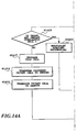
- FIGs. 12-14B An embodiment 4 is shown in Figs. 12-14B.
- Fig. 12 is a block diagram showing the configuration of the embodiment 4 of a multiplex transmitter 1201 in accordance with the present invention.
- Fig. 13 is a flowchart illustrating the processing logic of an extracting circuit 1206, and
- Figs. 14A and 14B are flowcharts illustrating the processing logic of a multiplexing processor 1207.
- the embodiment 4 of the multiplex transmitter in accordance with the present invention will now be described referring to Figs. 12-14B.
- the embodiment 4 differs from that in that it employs loadable data length x onto the next cell, which is provided from the multiplexing processor 1207. To achieve this in the embodiment 4, the multiplexing processor 1207 notifies an extracting circuit 1206 of the data length x that can be multiplexed into the next standard ATM cell to be subjected to the multiplex processing.
- the extracting circuit 1206 and multiplexing processor 1207 in the embodiment 4 of the multiplex transmitter 1201 as shown in Fig. 12 differ in operation from their counterparts of the embodiment 2. Since the operation of the other circuits is the same as that of the embodiment 3, only the operation of the two circuits will be described, omitting the description of the other circuits.
- the extracting circuit 1206 in Fig. 12 extracts the micro-frames from the buffers 1-m in accordance with the processing timing as in the embodiment 3, and transfers the micro-frames to be multiplexed to the multiplexing processor 1207.
- the criterion for the number of micro-frames to be extracted from the buffer is a fixed number k in the embodiment 3, the embodiment 4 uses the loadable data length x to the next cell, which is sent from the multiplexing processor 1207.
- the multiplexing processor 1207 decides the overlapping loading onto the next term cell, or the prolonged loading of the micro-frame extracted at the present timing onto the next timing cell, while carrying out the loading processing in accordance with a predetermined loading method, and detects the loadable data length to the next term cell.
- the multiplexing processor 1207 notifies the extracting circuit 1206 of the loadable data length x.
- the extracting circuit 1206 selects one of the buffers 1205 (S1303), and extracts a micro-frame (S1307).
- the selection logic of the buffer for the extraction is the same as that described in the flowchart of Fig. 10, for example.
- the accumulated data length ⁇ L(n) of the extracted micro-frames is compared with the data length x fed from the multiplexing processor 1207 (S1309). The extraction continues until the accumulated data length exceeds x, or the extraction processing time elapses (S1313).
- the notifications 1 and 2 to the multiplexing processor 1207 have the same meaning as in the embodiment 3.
- the extracting circuit 1206 decides the overlapping loading onto the next cell as shown at S1309 in the flowchart of Fig. 13, the dwell time of the finally extracted micro-frame in the buffer i plus the time period until the transfer of the next cell is compared with the cancellation tolerable time ti of the buffer i as in the embodiment 2 (S1321). If it exceeds the cancellation tolerable time ti, the finally extracted micro-frame is canceled (S1323), and the extracting processing is continued.
- the extracting circuit 1206 makes the branching by simply comparing the accumulated data length with x in this embodiment, the accumulated data length can be determined taking account of a data amount added in proportion to the number of multiplexed micro-frames during their multiplexing.
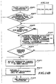
- Figs. 14A and 14B show the flowchart of the processing logic of the multiplexing processor 1207.
- the processing branches depending on the notification from the extracting circuit 1206 (S1403).
- notification 1 if there is no cell to be extracted and no overlapped residual data to be sent (NO at S1415), the idle cell is selected (S1417) to adjust transmission rate.
- the multiplexing processor 1207 carries out the micro-frame multiplexing onto the standard cell in accordance with the predetermined multiplexing method (S1407).
- it detects the accumulated loadable data length x onto the next term cell by comparing the data amount loadable in the next term with the residual data amount of the overlapping, and notifies the extracting circuit 1206 of the x (S1411).
- pattern 2 the idle cell or the multiplexed cell is transferred to a sender 1208 in accordance with the timing of the sender 1208 (S1413) and is transmitted.
- sendable portions are transferred to the sender 1208 at their occurrence (S1407).
- the foregoing embodiments 3 and 4 employs only one set of buffers instead of two sets of buffers consisting of the multiplex queuing buffers and transmission queuing buffers of the embodiments 1 and 2. This enables the multiplex transmitter to reduce the delay therein, and micro-frames of different service types to be multiplexed onto the same ATM cell.
- Figs. 15A-17 show an embodiment 5.
- Figs. 15A, 15B, 16A and 16B are block diagrams each showing a configuration of an ATM cell transmitter of the embodiment 5 in accordance with the present invention.
- Fig. 17 is a time chart illustrating the processing timings associated with an ATM cell transmitter 1601 as shown in Figs. 16A and 16B.
- An ATM cell transmitter 1501 shown in Figs. 15A and 15B simultaneously controls the micro-frame multiplexed ATM cells, which are delivered from a multiplex transmitter 1503 having the same configuration as its counterparts of the embodiment 1 or 2 of the present invention as shown in Figs. 1A-6, and standard ATM cells which are input to an interface 1505 of the ATM cell transmitter 1501, and sends them to the output channel.
- the ATM cells input through the interface 1505 are distributed by a distributor 1507 in accordance with the service types of the connections, and are stored in transmission queuing buffers 1509.
- the multiplex transmitter 1503 has the same configuration as those described in connection with Figs. 1A-6. Accordingly, the micro-frames input to an interface 1521 are multiplexed through a distributor 1523, a multiplex queuing buffers 1525, and a multiplexing processor 1528, and are stored into transmission queuing buffers 1529 as the ATM cells.
- the distribution accords with the service condition of each connection or ATM cell. Since the service condition is generally determined connection by connection, the distributor distributes the connections individually. Alternatively, the distributor distributes the ATM cells or micro-frames using the distributing information attached to each of them, and stores them in the buffers.
- An extraction selector 1511 collectively manages the reading of the transmission queuing buffers 1509 and 1529, and selects the ATM cells stored in the buffers 1509 and 1529 in an appropriate extracting order, thereby sequentially outputting them to the output channel through a sender 1513.
- the extraction selector 1511 extracts the ATM cells from the transmission queuing buffers 1509 in accordance with predetermined logic provided by external selection information, and delivers them to the sender 1513.
- Several logics for selecting the ATM cell are conceivable as follows, for example.
- Figs. 16A and 16B shows an ATM cell transmitter 1601 which simultaneously controls the micro-frame multiplexed ATM cells, which are delivered from a multiplex transmitter 1603 having the same configuration as its counterparts of the embodiment 3 or 4 of the present invention as shown in Figs. 7-14B, and standard ATM cells which are input to an interface 1605 of the ATM cell transmitter 1601, and sends them to the output channel.
- the ATM cell transmitter 1601 as shown in Figs. 16A and 16B differs from the ATM cell transmitter 1501 in that the buffers controlled by an extraction selector 1611 in the multiplex transmitter 1603 are multiplex queuing buffers.
- the multiplex transmitters in the embodiments 3 and 4 do not use the transmission queuing buffers. For this reason the extraction selector 1611 controls two sets of buffers of different levels, that is, transmission queuing buffers 1609 storing the ATM cells, and multiplex queuing buffers 1625 storing the micro-frames.
- the unit time for processing the ATM cell is determined from the channel rate available for transmitting a single ATM cell from the sender.
- the unit time thus determined is the one ATM cell output duration in Fig. 17, which is equal to 53 ⁇ 8/output channel (bits/sec).
- the multiplex transmitter 1603 carries out the extracting processing and multiplex processing such that they have been completed within the one ATM cell output duration as described before in connection with Fig. 8 (pattern 2).
- the methods 1-5 described above can be used, for example.
- the present invention provides the concrete system configuration for achieving multiplex loading onto standard ATM cells a plurality of connections consisting of micro-frames including data shorter than the standard ATM cells which are proposed in various fashions.
- the multiplex transmitters can achieve efficient multiplex transmission processing while maintaining the quality of individual micro-frames having several tolerable wait times or micro-frame cancellation ratios.
Abstract
Description
Claims (10)
- A multiplex transmitter for performing multiplex transmission by loading a standard ATM cell with multiplexed connections composed of micro-frames each including data shorter than the standard ATM cell, said multiplex transmitter characterized by comprising:a distributor for distributing input micro-frames;multiplex queuing buffers for storing said input micro-frames which have been distributed;an extracting portion for extracting entire micro-frames in the multiplex queuing buffers when a predetermined extracting time comes, or when a number of the micro-frames in each of said multiplex queuing buffers reaches a predetermined number;a multiplexing processor for carrying out multiplex processing onto the standard ATM cell in accordance with a predetermined multiplexing scheme;a transmission queuing buffer for storing said ATM cell;a cell cancellation monitor portion for canceling a cell whose dwell time in the transmission queuing buffer reaches a predetermined canceling time;an extracting portion for extracting the ATM cell from the transmission queuing buffer; anda sender for transferring the extracted ATM cell to an output channel.
- A multiplex transmitter for performing multiplex transmission by loading a standard ATM cell with multiplexed connections composed of micro-frames each including data shorter than the standard ATM cell, said multiplex transmitter characterized by comprising:a distributor for distributing input micro-frames;multiplex queuing buffers for storing said input micro-frames which have been distributed;an extracting portion for extracting entire micro-frames in each of the multiplex queuing buffers when a predetermined extracting time comes, or when a total length of the micro-frames in each of said multiplex queuing buffers reaches a data length;a multiplexing processor for carrying out multiplex processing onto the standard ATM cell in accordance with a predetermined multiplexing scheme, and notifies said extracting portion of the data length loadable onto a next ATM cell;a transmission queuing buffer for storing said ATM cell;a cell cancellation monitor portion for canceling a cell whose dwell time in the transmission queuing buffer reaches a predetermined canceling time;an extracting portion for extracting the ATM cell from the transmission queuing buffer; anda sender for transferring the extracted ATM cell to an output channel.
- The multiplex transmitter as claimed in claim 1 or 2, characterized in that said distributor distributes said input micro-frames to the buffers having different multiplexing schemes in accordance with predetermined service conditions.
- The multiplex transmitter as claimed in claim 3, characterized in that said multiplexing processor determines extracting order from said buffers in accordance with the service conditions, extracts the micro-frames, and selects the multiplexing scheme in accordance with the service conditions.
- A multiplex transmitter for performing multiplex transmission by loading a standard ATM cell with multiplexed connections composed of micro-frames each including data shorter than the standard ATM cell, said multiplex transmitter characterized by comprising:a distributor for distributing input micro-frames;multiplex queuing buffers for storing said input micro-frames which have been distributed;a cell cancellation monitor portion for storing each input micro-frame into one of the buffers, for monitoring a dwell time of the micro-frame in the transmitter, and for canceling a micro-frame which dwells in the buffer for more than a predetermined canceling time;an extracting portion for successively extracting from the buffers the micro-frames in accordance with their input order, a number of extracted micro-frames being limited within a predetermined multiplexing number;a multiplexing processor for carrying out multiplex processing onto the standard ATM cell in accordance with a predetermined multiplexing scheme; anda sender for transferring the extracted ATM cell to an output channel.
- A multiplex transmitter for performing multiplex transmission by loading a standard ATM cell with multiplexed connections composed of micro-frames each including data shorter than the standard ATM cell, said multiplex transmitter characterized by comprising:a distributor for distributing input micro-frames;multiplex queuing buffers for storing said input micro-frames which have been distributed;a cell cancellation monitor portion for storing each input micro-frame into one of the buffers, for monitoring a dwell time of the micro-frame in the transmitter, and for canceling a micro-frame which dwells in the buffer for more than a predetermined canceling time;an extracting portion for successively extracting from the buffers the micro-frames in accordance with their input order until an accumulated data length of the micro-frames and additional data exceeds a data length loadable onto a cell to be sent in a next term, or until a predetermined extracting time period has elapsed,a multiplexing processor for carrying out multiplex processing onto the standard ATM cell in accordance with a predetermined multiplexing scheme, and for notifying said extracting portion of the data length loadable onto the cell to be sent in the next term; anda sender for transferring the extracted ATM cell to an output channel.
- The multiplex transmitter as claimed in claim 5 or 6, characterized in that said multiplex transmitter distributes said input micro-frames to the buffers having different multiplexing schemes or canceling times of the micro-frames in accordance with predetermined service conditions.
- The multiplex transmitter as claimed in claim 7, characterized in that said multiplexing processor determines extracting order from said buffers in accordance with the service conditions, extracts the micro-frames, and selects the multiplexing scheme in accordance with the service conditions.
- The multiplex transmitter as claimed in claim 1 or 2, characterized in that said extracting portion performs extracting control not only of the transmission queuing buffer which stores the ATM cell onto which the multiplexing has been carried out, but also of the transmission queuing buffer which stores the ATM cell onto which no multiplexing has been carried out.
- The multiplex transmitter as claimed in claim 5 or 6, characterized in that said extracting portion performs extracting control not only of said buffers which store multiplexed micro-frames, but also of a transmission queuing buffer which stores ATM cell onto which no multiplexing has been carried out.
Applications Claiming Priority (4)
| Application Number | Priority Date | Filing Date | Title |
|---|---|---|---|
| JP33754795 | 1995-12-25 | ||
| JP337547/95 | 1995-12-25 | ||
| JP33754795 | 1995-12-25 | ||
| PCT/JP1996/003764 WO1997023975A1 (en) | 1995-12-25 | 1996-12-24 | Multiplex transmitter for micro-frame |
Publications (3)
| Publication Number | Publication Date |
|---|---|
| EP0821506A1 true EP0821506A1 (en) | 1998-01-28 |
| EP0821506A4 EP0821506A4 (en) | 2001-01-31 |
| EP0821506B1 EP0821506B1 (en) | 2004-07-14 |
Family
ID=18309684
Family Applications (1)
| Application Number | Title | Priority Date | Filing Date |
|---|---|---|---|
| EP96942630A Expired - Lifetime EP0821506B1 (en) | 1995-12-25 | 1996-12-24 | Multiplex transmitter for micro-frame |
Country Status (7)
| Country | Link |
|---|---|
| US (1) | US6061354A (en) |
| EP (1) | EP0821506B1 (en) |
| KR (1) | KR100283979B1 (en) |
| CN (1) | CN1095266C (en) |
| CA (1) | CA2213673C (en) |
| DE (1) | DE69632908T2 (en) |
| WO (1) | WO1997023975A1 (en) |
Cited By (1)
| Publication number | Priority date | Publication date | Assignee | Title |
|---|---|---|---|---|
| US7474664B2 (en) * | 1998-08-21 | 2009-01-06 | Nippon Telegraph And Telephone Corporation | ATM switch for ensuring cell sequence |
Families Citing this family (13)
| Publication number | Priority date | Publication date | Assignee | Title |
|---|---|---|---|---|
| JP2970596B2 (en) * | 1997-06-10 | 1999-11-02 | 日本電気株式会社 | ATM communication device |
| CA2266440C (en) | 1997-07-23 | 2004-09-14 | Ntt Mobile Communications Network Inc. | Multiplex transmission system and band control method |
| JP3765914B2 (en) * | 1997-10-13 | 2006-04-12 | 富士通株式会社 | Short cell multiplexer |
| US6449276B1 (en) * | 1998-05-20 | 2002-09-10 | Nokia Telecommunications Oy | Method and apparatus for efficient switching of partial minicells in ATM adaptation layer 2 |
| JP2000332781A (en) * | 1999-05-19 | 2000-11-30 | Hitachi Ltd | Variable length packet switch |
| US6396829B1 (en) * | 1999-07-06 | 2002-05-28 | Lucent Technologies, Inc. | Communications channel synchronous micro-cell for integrating circuit and packet data transmissions |
| JP2001028588A (en) * | 1999-07-14 | 2001-01-30 | Hitachi Ltd | Cell exchange |
| US6618383B1 (en) * | 1999-12-28 | 2003-09-09 | Nortel Networks Limited | Serial interface for a broadband communications network |
| US6654376B1 (en) * | 1999-12-28 | 2003-11-25 | Nortel Networks Limited | ATM packet scheduler |
| SE0000908L (en) * | 2000-03-20 | 2001-09-21 | Ericsson Telefon Ab L M | Load regulation |
| FR2821509B1 (en) * | 2001-02-27 | 2003-05-30 | Thomson Csf | METHOD AND DEVICE FOR TRANSFERRING DATA IN A COMMUNICATION NETWORK HAVING LOW-RATE ARTERY |
| US20020174258A1 (en) * | 2001-05-18 | 2002-11-21 | Dale Michele Zampetti | System and method for providing non-blocking shared structures |
| US8199772B2 (en) * | 2008-06-25 | 2012-06-12 | Ciena Corporation | Systems and methods for synchronous generic framing protocol mapping |
Citations (2)
| Publication number | Priority date | Publication date | Assignee | Title |
|---|---|---|---|---|
| WO1992016066A1 (en) * | 1991-02-28 | 1992-09-17 | Stratacom, Inc. | Method and apparatus for routing cell messages using delay |
| US5509007A (en) * | 1992-01-16 | 1996-04-16 | Fujitsu Limited | Cell multiplexing apparatus handling multiple items of information |
Family Cites Families (13)
| Publication number | Priority date | Publication date | Assignee | Title |
|---|---|---|---|---|
| FR2545670B1 (en) * | 1983-05-04 | 1985-07-05 | Billy Jean Claude | MULTIPLEXER, DEMULTIPLEXER AND MULTIPLEXING-DEMULTIPLEXING EQUIPMENT WITH RECONFIGURABLE FRAMES |
| JPH02225261A (en) * | 1989-02-28 | 1990-09-07 | Nec Corp | Printing device |
| DE4010535A1 (en) * | 1990-04-02 | 1991-10-10 | Philips Patentverwaltung | COUPLING ELEMENT FOR AN ASYNCHRONOUS TIME MULTIPLE TRANSMISSION SYSTEM |
| CA2110029C (en) * | 1992-11-27 | 1997-05-06 | Shigeru Otsuka | Mobile radio communication system |
| JP2576368B2 (en) * | 1993-06-30 | 1997-01-29 | 日本電気株式会社 | Data multiplexer |
| JP2580955B2 (en) * | 1993-06-23 | 1997-02-12 | 日本電気株式会社 | Data multiplexing device and separating device |
| US5561466A (en) * | 1993-06-23 | 1996-10-01 | Nec Corporation | Video and audio data multiplexing into ATM cells with no dummy cell used and ATM cell demultiplexing |
| JP2626507B2 (en) * | 1993-09-24 | 1997-07-02 | 日本電気株式会社 | ATM cell assembly and disassembly device |
| JPH07202895A (en) * | 1993-12-28 | 1995-08-04 | Hitachi Ltd | System and device for cell multiplexing |
| JP3079000B2 (en) * | 1994-01-11 | 2000-08-21 | 株式会社エヌ・ティ・ティ・ドコモ | Mobile wireless communication system |
| EP0662778B1 (en) * | 1994-01-11 | 2005-10-12 | NTT DoCoMo, Inc. | Mobile radio communications system |
| JPH07336354A (en) * | 1994-06-06 | 1995-12-22 | Oki Electric Ind Co Ltd | Stm data/atm cell conversion method and device |
| JP3630460B2 (en) * | 1995-01-23 | 2005-03-16 | 富士通株式会社 | Data length correction system |
-
1996
- 1996-12-24 DE DE69632908T patent/DE69632908T2/en not_active Expired - Lifetime
- 1996-12-24 WO PCT/JP1996/003764 patent/WO1997023975A1/en active IP Right Grant
- 1996-12-24 US US08/894,585 patent/US6061354A/en not_active Expired - Fee Related
- 1996-12-24 CA CA002213673A patent/CA2213673C/en not_active Expired - Fee Related
- 1996-12-24 KR KR1019970705876A patent/KR100283979B1/en not_active IP Right Cessation
- 1996-12-24 CN CN96192145A patent/CN1095266C/en not_active Expired - Fee Related
- 1996-12-24 EP EP96942630A patent/EP0821506B1/en not_active Expired - Lifetime
Patent Citations (2)
| Publication number | Priority date | Publication date | Assignee | Title |
|---|---|---|---|---|
| WO1992016066A1 (en) * | 1991-02-28 | 1992-09-17 | Stratacom, Inc. | Method and apparatus for routing cell messages using delay |
| US5509007A (en) * | 1992-01-16 | 1996-04-16 | Fujitsu Limited | Cell multiplexing apparatus handling multiple items of information |
Non-Patent Citations (1)
| Title |
|---|
| See also references of WO9723975A1 * |
Cited By (1)
| Publication number | Priority date | Publication date | Assignee | Title |
|---|---|---|---|---|
| US7474664B2 (en) * | 1998-08-21 | 2009-01-06 | Nippon Telegraph And Telephone Corporation | ATM switch for ensuring cell sequence |
Also Published As
| Publication number | Publication date |
|---|---|
| EP0821506A4 (en) | 2001-01-31 |
| EP0821506B1 (en) | 2004-07-14 |
| KR19980702476A (en) | 1998-07-15 |
| DE69632908T2 (en) | 2005-07-14 |
| WO1997023975A1 (en) | 1997-07-03 |
| KR100283979B1 (en) | 2001-03-02 |
| CA2213673A1 (en) | 1997-07-03 |
| CN1176720A (en) | 1998-03-18 |
| CN1095266C (en) | 2002-11-27 |
| CA2213673C (en) | 2001-08-07 |
| DE69632908D1 (en) | 2004-08-19 |
| US6061354A (en) | 2000-05-09 |
Similar Documents
| Publication | Publication Date | Title |
|---|---|---|
| US6061354A (en) | Micro-frame multiplex transmitter | |
| US6839358B2 (en) | Relaying apparatus | |
| US5519700A (en) | Telecommunication system with synchronous-asynchronous interface | |
| EP0703718B1 (en) | Controller for ATM segmentation and reassembly | |
| JP2686872B2 (en) | Common memory switch and switching method for digital information signal routing | |
| KR100328642B1 (en) | Arrangement and method relating to packet flow control | |
| EP0762799A2 (en) | Burst transfer system | |
| US6414961B1 (en) | ATM switching with virtual circuit FIFO buffers | |
| EP0678996A2 (en) | Apparatus and method of processing bandwidth requirements in an ATM switch | |
| US6185188B1 (en) | Method and apparatus for controlling physical port flow rate in packet communications | |
| US5513174A (en) | Telecommunication system with detection and control of packet collisions | |
| JP2001223704A (en) | Packet transfer device | |
| EP0868042A2 (en) | Clock information transfer system for AAL type 1 transmission | |
| JPH11510665A (en) | Method for optimally transmitting ATM cells via connection elements | |
| CA2280782C (en) | Method and circuit arrangement for the transmission of message cells during the course of virtual connections having different priorities | |
| JP2001016226A (en) | Transmission control system for atm cell and transmission controller | |
| JP3016400B2 (en) | Micro frame multiplex transmitter | |
| US7130267B1 (en) | System and method for allocating bandwidth in a network node | |
| US5991267A (en) | Fixed-length cell multiplex transmission apparatus, fixed-length cell multiplex transmission method, fixed-length cell transmtting apparatus, fixed-length cell multiplexing apparatus, and fixed-length cell distributing apparatus | |
| JP2751832B2 (en) | ATM network and network configuration device | |
| US20020097735A1 (en) | Multiplexing and demultiplexing method and apparatus | |
| US7515591B1 (en) | Primary channel bank-resident mechanism for scheduling downstream data transmissions to ports of multiple channel banks | |
| KR100299312B1 (en) | apparatus and method for arbitration cell transmission in ATM switching system | |
| KR100306483B1 (en) | ATM Cell Mulitplexing System | |
| JPH08186577A (en) | Cell multiplexing method and cell transfer network |
Legal Events
| Date | Code | Title | Description |
|---|---|---|---|
| PUAI | Public reference made under article 153(3) epc to a published international application that has entered the european phase |
Free format text: ORIGINAL CODE: 0009012 |
|
| 17P | Request for examination filed |
Effective date: 19970829 |
|
| AK | Designated contracting states |
Kind code of ref document: A1 Designated state(s): DE FR GB IT SE |
|
| A4 | Supplementary search report drawn up and despatched |
Effective date: 20001215 |
|
| AK | Designated contracting states |
Kind code of ref document: A4 Designated state(s): DE FR GB IT SE |
|
| RIC1 | Information provided on ipc code assigned before grant |
Free format text: 7H 04L 12/28 A, 7H 04L 12/56 B, 7H 04Q 11/04 B |
|
| RAP1 | Party data changed (applicant data changed or rights of an application transferred) |
Owner name: NTT DOCOMO, INC. |
|
| 17Q | First examination report despatched |
Effective date: 20030416 |
|
| GRAP | Despatch of communication of intention to grant a patent |
Free format text: ORIGINAL CODE: EPIDOSNIGR1 |
|
| GRAS | Grant fee paid |
Free format text: ORIGINAL CODE: EPIDOSNIGR3 |
|
| GRAA | (expected) grant |
Free format text: ORIGINAL CODE: 0009210 |
|
| AK | Designated contracting states |
Kind code of ref document: B1 Designated state(s): DE FR GB IT SE |
|
| REG | Reference to a national code |
Ref country code: GB Ref legal event code: FG4D |
|
| REF | Corresponds to: |
Ref document number: 69632908 Country of ref document: DE Date of ref document: 20040819 Kind code of ref document: P |
|
| REG | Reference to a national code |
Ref country code: SE Ref legal event code: TRGR |
|
| ET | Fr: translation filed | ||
| PLBE | No opposition filed within time limit |
Free format text: ORIGINAL CODE: 0009261 |
|
| STAA | Information on the status of an ep patent application or granted ep patent |
Free format text: STATUS: NO OPPOSITION FILED WITHIN TIME LIMIT |
|
| 26N | No opposition filed |
Effective date: 20050415 |
|
| PGFP | Annual fee paid to national office [announced via postgrant information from national office to epo] |
Ref country code: FR Payment date: 20101224 Year of fee payment: 15 |
|
| PGFP | Annual fee paid to national office [announced via postgrant information from national office to epo] |
Ref country code: GB Payment date: 20101222 Year of fee payment: 15 Ref country code: IT Payment date: 20101224 Year of fee payment: 15 Ref country code: SE Payment date: 20101213 Year of fee payment: 15 |
|
| PGFP | Annual fee paid to national office [announced via postgrant information from national office to epo] |
Ref country code: DE Payment date: 20101222 Year of fee payment: 15 |
|
| REG | Reference to a national code |
Ref country code: SE Ref legal event code: EUG |
|
| GBPC | Gb: european patent ceased through non-payment of renewal fee |
Effective date: 20111224 |
|
| REG | Reference to a national code |
Ref country code: FR Ref legal event code: ST Effective date: 20120831 |
|
| REG | Reference to a national code |
Ref country code: DE Ref legal event code: R119 Ref document number: 69632908 Country of ref document: DE Effective date: 20120703 |
|
| PG25 | Lapsed in a contracting state [announced via postgrant information from national office to epo] |
Ref country code: DE Free format text: LAPSE BECAUSE OF NON-PAYMENT OF DUE FEES Effective date: 20120703 Ref country code: GB Free format text: LAPSE BECAUSE OF NON-PAYMENT OF DUE FEES Effective date: 20111224 Ref country code: SE Free format text: LAPSE BECAUSE OF NON-PAYMENT OF DUE FEES Effective date: 20111225 |
|
| PG25 | Lapsed in a contracting state [announced via postgrant information from national office to epo] |
Ref country code: IT Free format text: LAPSE BECAUSE OF NON-PAYMENT OF DUE FEES Effective date: 20111224 |
|
| PG25 | Lapsed in a contracting state [announced via postgrant information from national office to epo] |
Ref country code: FR Free format text: LAPSE BECAUSE OF NON-PAYMENT OF DUE FEES Effective date: 20120102 |