EP0827220A2 - Methods and compositions for optimizing interfacial properties of transducers used in data storage devices - Google Patents

Methods and compositions for optimizing interfacial properties of transducers used in data storage devices Download PDF

Info

Publication number
EP0827220A2
EP0827220A2 EP97114191A EP97114191A EP0827220A2 EP 0827220 A2 EP0827220 A2 EP 0827220A2 EP 97114191 A EP97114191 A EP 97114191A EP 97114191 A EP97114191 A EP 97114191A EP 0827220 A2 EP0827220 A2 EP 0827220A2
Authority
EP
European Patent Office
Prior art keywords
spacer
selecting
electronegativity
data storage
storage device
Prior art date
Legal status (The legal status is an assumption and is not a legal conclusion. Google has not performed a legal analysis and makes no representation as to the accuracy of the status listed.)
Withdrawn
Application number
EP97114191A
Other languages
German (de)
French (fr)
Other versions
EP0827220A3 (en
Inventor
Daniel A. Nepela
Current Assignee (The listed assignees may be inaccurate. Google has not performed a legal analysis and makes no representation or warranty as to the accuracy of the list.)
Read Rite Corp
Original Assignee
Read Rite Corp
Priority date (The priority date is an assumption and is not a legal conclusion. Google has not performed a legal analysis and makes no representation as to the accuracy of the date listed.)
Filing date
Publication date
Application filed by Read Rite Corp filed Critical Read Rite Corp
Publication of EP0827220A2 publication Critical patent/EP0827220A2/en
Publication of EP0827220A3 publication Critical patent/EP0827220A3/en
Withdrawn legal-status Critical Current

Links

Images

Classifications

    • GPHYSICS
    • G01MEASURING; TESTING
    • G01RMEASURING ELECTRIC VARIABLES; MEASURING MAGNETIC VARIABLES
    • G01R33/00Arrangements or instruments for measuring magnetic variables
    • G01R33/02Measuring direction or magnitude of magnetic fields or magnetic flux
    • G01R33/06Measuring direction or magnitude of magnetic fields or magnetic flux using galvano-magnetic devices
    • G01R33/09Magnetoresistive devices
    • G01R33/093Magnetoresistive devices using multilayer structures, e.g. giant magnetoresistance sensors
    • BPERFORMING OPERATIONS; TRANSPORTING
    • B82NANOTECHNOLOGY
    • B82YSPECIFIC USES OR APPLICATIONS OF NANOSTRUCTURES; MEASUREMENT OR ANALYSIS OF NANOSTRUCTURES; MANUFACTURE OR TREATMENT OF NANOSTRUCTURES
    • B82Y10/00Nanotechnology for information processing, storage or transmission, e.g. quantum computing or single electron logic
    • BPERFORMING OPERATIONS; TRANSPORTING
    • B82NANOTECHNOLOGY
    • B82YSPECIFIC USES OR APPLICATIONS OF NANOSTRUCTURES; MEASUREMENT OR ANALYSIS OF NANOSTRUCTURES; MANUFACTURE OR TREATMENT OF NANOSTRUCTURES
    • B82Y25/00Nanomagnetism, e.g. magnetoimpedance, anisotropic magnetoresistance, giant magnetoresistance or tunneling magnetoresistance
    • BPERFORMING OPERATIONS; TRANSPORTING
    • B82NANOTECHNOLOGY
    • B82YSPECIFIC USES OR APPLICATIONS OF NANOSTRUCTURES; MEASUREMENT OR ANALYSIS OF NANOSTRUCTURES; MANUFACTURE OR TREATMENT OF NANOSTRUCTURES
    • B82Y40/00Manufacture or treatment of nanostructures
    • GPHYSICS
    • G11INFORMATION STORAGE
    • G11BINFORMATION STORAGE BASED ON RELATIVE MOVEMENT BETWEEN RECORD CARRIER AND TRANSDUCER
    • G11B5/00Recording by magnetisation or demagnetisation of a record carrier; Reproducing by magnetic means; Record carriers therefor
    • G11B5/127Structure or manufacture of heads, e.g. inductive
    • G11B5/33Structure or manufacture of flux-sensitive heads, i.e. for reproduction only; Combination of such heads with means for recording or erasing only
    • G11B5/39Structure or manufacture of flux-sensitive heads, i.e. for reproduction only; Combination of such heads with means for recording or erasing only using magneto-resistive devices or effects
    • G11B5/3903Structure or manufacture of flux-sensitive heads, i.e. for reproduction only; Combination of such heads with means for recording or erasing only using magneto-resistive devices or effects using magnetic thin film layers or their effects, the films being part of integrated structures
    • HELECTRICITY
    • H01ELECTRIC ELEMENTS
    • H01FMAGNETS; INDUCTANCES; TRANSFORMERS; SELECTION OF MATERIALS FOR THEIR MAGNETIC PROPERTIES
    • H01F41/00Apparatus or processes specially adapted for manufacturing or assembling magnets, inductances or transformers; Apparatus or processes specially adapted for manufacturing materials characterised by their magnetic properties
    • H01F41/14Apparatus or processes specially adapted for manufacturing or assembling magnets, inductances or transformers; Apparatus or processes specially adapted for manufacturing materials characterised by their magnetic properties for applying magnetic films to substrates
    • H01F41/30Apparatus or processes specially adapted for manufacturing or assembling magnets, inductances or transformers; Apparatus or processes specially adapted for manufacturing materials characterised by their magnetic properties for applying magnetic films to substrates for applying nanostructures, e.g. by molecular beam epitaxy [MBE]
    • H01F41/302Apparatus or processes specially adapted for manufacturing or assembling magnets, inductances or transformers; Apparatus or processes specially adapted for manufacturing materials characterised by their magnetic properties for applying magnetic films to substrates for applying nanostructures, e.g. by molecular beam epitaxy [MBE] for applying spin-exchange-coupled multilayers, e.g. nanostructured superlattices
    • HELECTRICITY
    • H10SEMICONDUCTOR DEVICES; ELECTRIC SOLID-STATE DEVICES NOT OTHERWISE PROVIDED FOR
    • H10NELECTRIC SOLID-STATE DEVICES NOT OTHERWISE PROVIDED FOR
    • H10N50/00Galvanomagnetic devices
    • H10N50/10Magnetoresistive devices
    • HELECTRICITY
    • H10SEMICONDUCTOR DEVICES; ELECTRIC SOLID-STATE DEVICES NOT OTHERWISE PROVIDED FOR
    • H10NELECTRIC SOLID-STATE DEVICES NOT OTHERWISE PROVIDED FOR
    • H10N50/00Galvanomagnetic devices
    • H10N50/80Constructional details
    • H10N50/85Magnetic active materials
    • GPHYSICS
    • G11INFORMATION STORAGE
    • G11BINFORMATION STORAGE BASED ON RELATIVE MOVEMENT BETWEEN RECORD CARRIER AND TRANSDUCER
    • G11B5/00Recording by magnetisation or demagnetisation of a record carrier; Reproducing by magnetic means; Record carriers therefor
    • G11B5/127Structure or manufacture of heads, e.g. inductive
    • G11B5/33Structure or manufacture of flux-sensitive heads, i.e. for reproduction only; Combination of such heads with means for recording or erasing only
    • G11B5/39Structure or manufacture of flux-sensitive heads, i.e. for reproduction only; Combination of such heads with means for recording or erasing only using magneto-resistive devices or effects
    • G11B2005/3996Structure or manufacture of flux-sensitive heads, i.e. for reproduction only; Combination of such heads with means for recording or erasing only using magneto-resistive devices or effects large or giant magnetoresistive effects [GMR], e.g. as generated in spin-valve [SV] devices
    • GPHYSICS
    • G11INFORMATION STORAGE
    • G11BINFORMATION STORAGE BASED ON RELATIVE MOVEMENT BETWEEN RECORD CARRIER AND TRANSDUCER
    • G11B5/00Recording by magnetisation or demagnetisation of a record carrier; Reproducing by magnetic means; Record carriers therefor
    • G11B5/40Protective measures on heads, e.g. against excessive temperature 

Definitions

  • This invention relates to methods and compositions for optimizing the interfacial properties of data storage devices, such as spin valve sensors and giant magnetoresitance (GMR) sensors.
  • data storage devices such as spin valve sensors and giant magnetoresitance (GMR) sensors.
  • GMR giant magnetoresitance
  • Still another object of the present invention is to maximize the signal output, as represented by % ⁇ R/R of spin valve sensors and giant magnetoresistance (GMR) sensors.
  • Yet another object of this invention is to maximize the corrosion resistance of spin valve sensors and giant magnetoresistance sensors.
  • the present invention proposes an empirical relationship between % ⁇ R/R and the electronegativity difference between adjacent FM layers and conductive spacers in spin valve and GMR sensors.
  • Such a general empirical relationship applies to both spin valve and GMR sensors, and shows that % ⁇ R/R response is a function of the electronegativity mismatch between adjacent FM layers and conductive spacers.
  • mismatch in electronegativities
  • Each chemical element has a work function ⁇ from which the ⁇ of that element is computed by either equations (1a) or (1b) that are equivalent.
  • the ⁇ of such alloys has been found to be an additive property of the constituents of the alloy, so that the ⁇ of the alloy is the sum of the products of the atomic fraction of any element in the alloy times the electronegativity of that element summed over all elements constituting the alloy, as expressed in equation (2).
  • Fig. 2 illustrates the use of the present inventive concept in a giant magnetoresistive (GMR) sensor 20.
  • the GMR sensor 20 is a sandwich structure formed of a plurality of layers, such as FM, that are separated by a plurality of conductive spacers 22.
  • the FM/spacer structure can have a multiplicity of 5 to 75 repeat units of FM/spacers.
  • the electronegativities of each of the successive layers FM are substantially matched or their difference in ⁇ is minimized with the electronegativity of the contiguous spacers 22.
  • Prior art methods for fabricating spin valve and GMR sensors included combining spacers made of an adequately electrically conductive material such as Au, Ag or Cu, with layers of FM materials such as FeCo alloy or NiFe alloy, or elements Fe, Co and Ni, without regard to the electronegativity matching between the successive FM layers and conductive spacers. These prior art methods are mainly based on trial and error studies.
  • This example illustrates that the atomic fraction of the electronegativities ( ⁇ 's) of the elements of any alloy conductor or ferromagnet formed of any number of elements, i.e., ternary, quaternary, etc., can be used to calculate the electronegativity of the alloy.
  • Table I it is possible to closely match the electronegativities of the conductors and the ferromagnets. For example, having selected Cu 3 Pt as the conductor of choice, it would be desirable to select a FM material having a close electronegativity. Table I indicates that one of the closest materials whose electronegativity matches that of Cu 3 Pt is NiMn, since the average electronegativity of Ni 3 Mn is 2.02 and ⁇ ⁇ 0
  • a superlattice intermetallic compound having an electronegativity of 2.02 may be matched with Cu 3 Pt.
  • the matching of two superlattice structures is desirable in that these ordered structures will improve the thermal stability of the device containing them, since additional external thermal energy would be required to disorder one or both superlattice structures before the elements contained in superlattice were free to diffuse at the interface. This additional energy ranges between 0.1 eV to 0.3 eV above the activation energy for cross diffusion at the interface between the conductor spacer and the FM layer.
  • Point D on curve S1 represents the following composition:Co - Cu - CO, where the first element (Co) is the unpinned FM layer FM1, the second element [Cu] is the conductive spacer 12, and the third element [Co] is the pinned FM layer FM2.
  • the composition of this example yields a % ⁇ R/R of approximately 9.5%.
  • Point H on curve S1 represents Ni- Cu -Ni, where the first element (Ni) is the unpinned FM layer FM1, the second element [Cu] is the conductive spacer 12, and the third element [Ni] is the pinned FM layer FM2.
  • the composition of this example yields a % ⁇ R/R of approximately 2.5%.
  • Point I on curve S1 represents [80Ni 20Fe]-[Pt]-[80Ni 20Fe], where the first element [80Ni 20Fe] is the unpinned FM layer FM1, the second element [Pt] is the conductive spacer 12, and the third element [80Ni 20Fe] is the pinned FM layer FM2.
  • the composition of this example yields a % ⁇ R/R of approximately 0.3%.
  • Point K on curve S1 represents [80Ni 20Fe]-[Al]-[80Ni 20Fe], where the first element [80Ni 20Fe] is the unpinned FM layer FM1, the second element [Al] is the conductive spacer 12, and the third element [80Ni 20 Fe] is the pinned FM layer FM2.
  • 1/2 between Al and its adjacent NiFe layer FM1 is approximately 0.6/eV, which is greater than the intercept point value of 0.5 eV. In this and other similar examples where
  • Fig. 4 graphically illustrates the linear relationships between the % ⁇ R/R of the spin valve sensor 10 (Fig. 1) relative to the square root of the absolute value of the electronegativity difference (
  • the response is shown at three different measurement temperatures, that is, 300°K, 200°K and 100°K.
  • the conductive spacer separating the FMs is generally between 18A° and 30° thick, while the FMs generally range between 30A° and 120A° with an optimum thickness typically at 60A° each.
  • Fig. 5 graphically illustrates linear relationships between % ⁇ R/R of the GMR sensor 20 (Fig. 2) relative to the square root of the electronegativity difference
  • the curves G1, G2, G3 may be expressed generally by the following equations (6), (7) and (8), that continue to confirm equations (3) and (4).
  • the present analysis recognizes the need for optimizing the roughness of the interface for maximizing % ⁇ R/R for any particular interface. Accordingly, the curves G1, G2, G3 take into consideration the fact that different experimenters may conduct their experiments under different conditions, such as different substrate temperatures, different deposition rates, different Argon background sputtering pressure, and thus will realize different degrees of interfacial roughness. Again we reiterate that the interfacial surface roughness will vary the slopes of curves G1, G2 and G3 and that some optimum roughness exists that maximizes % ⁇ R/R for any interface ⁇ of the FM and spacer layers.
  • points R1 and S1 correspond to the respective compositions of points J1, H1, and M1 along the first peak curve G1.
  • V1 is Ni30-Co70
  • W1 is Ni50-Co50
  • X1 is Ni70-Co30
  • Y1 is Ni.
  • Fig. 6 graphically illustrates three linear relationships between % ⁇ R/R of the GMR sensor 20 (Fig. 2) relative to the square root of the electronegativity difference
  • Curve R1 may be expressed by the following equation (9), and relates to the GMR first peak: % ⁇ R/R ⁇ 330 - 660
  • Curve R2 may be expressed by the following equation (10), and relates to the second GMR peak: (10) % ⁇ R/R ⁇ 158 - 316 (
  • the exemplary compositions are expressed as follows X-Y, where element X represents the material for the FM layers FM, and element "Y" represents the material for the conductive spacers 22.
  • points m1 and n1 correspond to the respective compositions of points i1 (Co/Cu), and j1 (Co/Ag) along the first peak curve G1.
  • Point "p” relates to the GMR structure Fe - Cu.
  • This structure presents an almost perfect electronegativity match i. e., ( ⁇ ⁇ 0) between the Fe and Cu layers, nonetheless, this structure does not provide a high % ⁇ R/R since Fe is a BCC element, while Cu is a FCC element. Accordingly extremely inferior % ⁇ R/R is obtained and equations (3 and 4) are not obeyed due to potential barriers created by the lattice type mismatch, that is, BCC/FCC.
  • Fig. 9 shows two graphs SL3, SL4, plotting the electrical resistivity in micro ohmcm versus the atomic composition for the Cu-Pt superlattice system.
  • Graph SL3 illustrates the relationship for alloys that are quenched and cold worked (disordered state).
  • Graph SL4 illustrates the relationship for alloys that are annealed at 300°C for rendering an ordered superlattice structure.
  • Fig. 9 further shows that the specific electrical resistivities of the ordered superlattice may be reduced significantly by annealing the alloys at two critical points CP3 (25% atomic percent Pt), and CP4 (50% atomic percent Pt).
  • the two alloy series in examples 24 and 25 may be annealed at between 120 °C to 250 °C in thin film form for approximately 0.5 hour to 4 hours to form the superlattice at appropriate composition.
  • the present invention proposes the use of superlattices processed at or near critical points CP or within any of the shaded regions in the CuAu binary systemor the CuPtbinary system.
  • the shaded regions define the composition range within which some degree of superlattice order will occur and which may be used advantageously.
  • the most advantageous compositions from a resistivity point of view are a 25 and 50 atomic % for both the CuAu and CuPt.
  • a superlattice spacer 22 will provide a large mean free path in the spacer while simultaneously minimizing the electronegativity difference
  • 50:50 CuAu superlattice alloy (Fig. 9) exhibits a resistivity of about 3.5 ⁇ -cm, which is similar to the resistivity of gold, and an average electronegativity ( ⁇ ) of approximately 2.07 eV.
  • a 50:50 CuAu superlattice ( Figure 5) is used as a spacer, while an Ni 3 Fe superlattice composition forms the FM layers.
  • the average electronegativity of the 50:50 CuAu superlattice is about 2.07, which has an absolute electronegativeity difference of about 0.01 with N 13 Fe.
  • one method for processing the superlattice is to anneal the alloys between 120°C to 250°C for 10 to 200 minutes.
  • An alternative method is to deposit the superlattice alloys by sputtering or evaporation, at a relatively low rate, on a sufficiently heated substrate. This slow deposition process could form the superlattice structure without the need for annealing.
  • the alloys that are used to achieve the preceding objectives are from the group constituting Fe, Ni, Co or any combination of these elements, and alloys thereof which, may be alloyeed with elements or combination thereof from the group consisting of Au, Cu, Mn, Ti, V, Pt, Pd, Ru, Ir, Sn, Ta, Nb, Rh, N, C, Zr, Hf, Y, La, and rare earth elements, either in crystalline FCC or BCC form or in amorphous form containing a combination of the above elements.
  • a group of quaternary FM alloys with minimal magnetostriction includes: [48Co - 29Ni - 23Fe] 1-yPd. [26Co - 44Ni - 30Fe] 1-yPd.
  • y represents the atomic fraction
  • these alloys display near zero magnetostriction and low overcivity. More specifically, the following alloys have near zero magnetostriction and have ⁇ values of 2.13.
  • Each alloy can be matched with the superlattice composite conductive spacer of CuPt whose ⁇ is approximately 2.12. 33.6Co - 20.3Ni - 16.1Fe - 30Pd. 18.2Co - 30.8Ni - 21Fe - 30Pd.
  • Fig. 10 illustrates the use of single crystals in the spin valve sensor 10 of Fig. 1.
  • the surface crystalline orientation of the substrate has been selected to be 111.
  • the subsequent single crystal layers that are formed on top of the substrate will automatically assume the same 111 surface orientation. It is an object of the present invention to match the electronegativities of the selected crystalline orientation or face, which in this example is 111, of the juxtaposed layers, rather than to match the average electronegativities of these layers.
  • Fig. 11 illustrates the use of polycrystals in the spin valve sensor 10 of Fig. 1.
  • the crystalline orientation of the substrate is random, and therefore the three main crystallographic orientations, i.e., 100, 110, 111 have approximately the same frequency of surface occupancy on the substrate.
  • the subsequent polycrystal layers FM and AFM that are formed on top of the substrate will automatically assume the same random orientation as the substrate by epitaxy of the underlying polycrystals of the prior spacer or FM layer FM. It is an object of the present invention to match the average electronegativity of each layer to the average electronegativity of the adjacent layers.
  • the spin valve sensor 10 is formed by selecting the desired spacer material. Subsequently, the FM layers FM1 and FM2 are selected such that their average electronegativities match or substantially approximate the average electronegativity of the selected spacer 12.
  • the following example 29 illustrates the impact of the mismatch of the electronegativity (
  • the selection of crystal orientation, 111, 100 or 110 can be accomplished by selecting a single crystal substrate such as single crystal magnesium oxide with surface orientations of either 111, 100 or 110.
  • a single orientation for example 111 of the substrate and subsequently selecting a ferromagnet and conductive spacer whose ⁇ 's are minimized, and subsequently depositing alternating layers of FM and conductive spacers on such an oriented substrate, results in % ⁇ R/R's that will be greater than randomly oriented polycrystalline structures.
  • AgAu alloys may be used as well with Au less than 25 atomic %.

Landscapes

  • Engineering & Computer Science (AREA)
  • Nanotechnology (AREA)
  • Chemical & Material Sciences (AREA)
  • Crystallography & Structural Chemistry (AREA)
  • Physics & Mathematics (AREA)
  • Manufacturing & Machinery (AREA)
  • General Physics & Mathematics (AREA)
  • Condensed Matter Physics & Semiconductors (AREA)
  • Power Engineering (AREA)
  • Spectroscopy & Molecular Physics (AREA)
  • Mathematical Physics (AREA)
  • Theoretical Computer Science (AREA)
  • Hall/Mr Elements (AREA)
  • Micromachines (AREA)
  • Magnetic Heads (AREA)

Abstract

A method for maximizing the interfacial properties of sensors (10), such as spin valve and GMR sensors (10), used in storage devices, comprises selecting the materials for ferromagnetic layers (FM1, FM2) and for electrically conductive spacers (12) that are interposed between the ferromagnetic layers (FM1, FM2). The electronegativities of the selected materials are substantially matched so that the differences in electronegativities is minimized. The conductive spacer (12) material provides a relatively low resistivity and/or a large mean free path. The sensors (10) experience greater chemical and thermal stability, are corrosion resistant, and realize an increased signal output.

Description

Field of the Invention
This invention relates to methods and compositions for optimizing the interfacial properties of data storage devices, such as spin valve sensors and giant magnetoresitance (GMR) sensors.
Description of the Prior Art
Significant progress has occurred over the past two decades in the design of multilayered nanostructured thin film systems. The prior art describes large GMR current-in-plane (CIP) effects in an Fe/Cr multilayered system, approximating a GMR effect (%ΔR/R) of 100%, that is change by a factor of two in resistance with an adequate external field. Since then, many other multilayer GMR and spin valve sensors have been explored. To date, the highest GMR effect is in the Fe/Cr system and is approximately 150% at a measurement temperature of 5°K, and remains the largest value observed at any temperature to date. The GMR effect is characterized by %ΔR/R, which is defined as the change in resistance divided by the initial resistance, and is
100 (R0-RH)/R0, where R0 is without an external magnetic field and RH is at maximun external field.
Numerous theoretical studies have attempted to explain the behavior of spin valve and GMR effects, and thus far there does not exist a uniform, universally accepted explanation of the main factors controlling the magnitude of the response as characterized by %ΔR/R. On the experimental side, efforts have been largely based on trial and error, by experimenting with various combinations of ferromagnetic layers and conductive spacer layers. None of the previous work has yielded quantitative guidelines for the maximization of %ΔR/R for spin valve or GMR sensors by providing selection criteria for the proper layer compositions of the ferromagnetic material and the conductive spacer.
Summary of the Invention
An object of this invention is to provide means and methods for optimizing the manufacturing process of various devices, including but not limited to thin film devices such as sensors used in data storage devices.
Another object of this invention is to provide quantitative guidelines for optimizing the selection of multi-layer compositions by matching or minimizing the difference in the interfacial electronegativities of adjacent ferromagnetic layersand conductive spacers.
Still another object of the present invention is to maximize the signal output, as represented by %ΔR/R of spin valve sensors and giant magnetoresistance (GMR) sensors.
A further object of this invention is to maximize the thermal stability of spin valve sensors and giant magnetoresistance sensors.
Yet another object of this invention is to maximize the corrosion resistance of spin valve sensors and giant magnetoresistance sensors.
Another object is to provide for multiple interfacial matching of a ferromagnetic layer with its contacting conductive spacers.
In accordance with this invention, spin valve sensors and GMR sensors are made with layers of ferromagnetic (FM) material and conductive spacers interposed between the FM layers. The difference in electronegativities between the layers and spacers is minimized. A relatively low resistivity and/or a large mean free path is provided by the conductive spacer material. As a result of these conditions, the %ΔR/R of the sensor is maximized. The novel sensor is corrosion resistant, and experiences greater chemical and thermal stability, and signal output of the sensor device is increased.
a method for optimizing the interfacial properties of a data storage device. The inventive method includes selecting one or more electrically conductive spacers having at least a first electronegativity (χ spacer), and selecting one or more FM layers having at least a second electronegativity (χ FM), such that the selecting steps include the step of substantially matching the first and second electronegativities and minimizing the difference between the electronegativities.
Brief Description of the Drawing
The invention will be described in greater detail with reference to the drawing in which:
  • Fig. 1 is a diagrammatic cross-sectional view depicting a spin valve sensor made in accordance with this invention;
  • Fig. 2 is a diagrammatic cross-sectional view depicting a GMR sensor made in accordance with this invention;
  • Fig. 3 is a graph plotting the relationship of the electronegativity difference (|Δχ|1/2) versus %ΔR/R for spin valve sensors with different ferromagnet/conductive spacer interfaces;
  • Fig 4 illustrates three graphs plotting the relationship of the electronegativity difference (|Δχ|1/2) versus %ΔR/R for Co, NiFe, Ni spin valve sensors with a constant thickness copper spacer of approximately 60A;
  • Fig. 5 illustrates three graphs plotting the relationship of the electronegativity difference (|Δχ|1/2) versus %ΔR/R for various CoNi alloys including Co and Ni as FM layers illustrating the first, second and third peaks of GMR response;
  • Fig. 6 illustrates three graphs plotting the relationship of the electronegativity difference (|Δχ|1/2) versus %ΔR/R for various FM/conductive spacer interfaces including CoCr, CoCu and CoAg as FM layers for the first, second and third peaks of GMR response;
  • Fig. 7 is a chart that graphically illustrates various exemplary combinations and compositions of FM layers and spacers for use in spin valve and GMR sensors;
  • Fig. 8 illustrates two graphs plotting the electrical resistivity in microOhm-cm versus the atomic composition for a Cu-Au superlattice system;
  • Fig. 9 illustrates two graphs plotting the electrical resistivity in microOhm-cm versus the atomic composition for a CuPt superlattice system;
  • Fig. 10 illustrates the use of single crystal orientation in a spin valve sensor made according to the present invention;
  • Fig. 11 illustrates the use of polycrystalline randon orientation in a spin valve sensor made according to the present invention;
  • Fig. 12 is a cross-sectional view of a spin valve sensor with compound interfaces made according to the present invention; and
  • Fig. 13 is a cross-sectional view of a giant magnetoresistance sensor with compound interfaces made according to the present invention.
  • Similar numerals refer to similar elements in the drawing. It should be understood that the sizes of the different components in the figures are not necessarily in exact proportion, and are shown for visual clarity and for the purpose of explanation.
    Detailed Description of the Invention
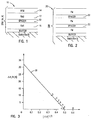
    Fig. 1 is a partial cross-section reprresenting a spin valve magnetoresistive (MR) sensor 10 made according to the present invention. The spin valve sensor 10 is formed of two FM layers FM1, FM2 that are separated by a conductive spacer or layer 12. The sensor 10 is formed on a nonmagnetic substrate on which a buffer layer, about 25-100 Angstroms thick, is deposited. The buffer layer is made from Ta, Cr, Fe, Pt, Pd, Ir or Au. The FM layers FM1 and FM2 may have the same or different composition. The magnetization of the FM layer FM2 is pinned by placing it in atomic contact with an antiferromagnetic (AFM) layer 14, such as an iron-manganese (FMn) layer. The magnetization of the unpinned FM layer FM1 is free to rotate in the presence of an external magnetic field.
    The application of an external magnetic field causes a variation in the magnetization orientation of the FM layer FM1, which causes a change in the spin-dependent scattering of conduction electrons and thus in the electrical resistance of the spin valve sensor 10. The resistance of the spin valve sensor 10 changes as the relative alignment of the magnetization of the FM1 layer changes. The FM2 layer remains constrained and its magnetization direction renmains the same.
    The present invention proposes an empirical relationship between %ΔR/R and the electronegativity difference between adjacent FM layers and conductive spacers in spin valve and GMR sensors. Such a general empirical relationship applies to both spin valve and GMR sensors, and shows that %ΔR/R response is a function of the electronegativity mismatch between adjacent FM layers and conductive spacers. It is applicant's belief that the mismatch in electronegativities (χ)s results in a potential barrier at the interface that is related to the absolute value of the difference in the electronegativities of the FM layers and the conductive spacers, i.e.,Δχ. With increasing Δχ mismatch, the %ΔR/R amplitude of the spin valve and GMR sensors will decrease to a point where %ΔR/R will approach an intercept value of zero. As shown later, this intercept value uniformly occurs at a value of |Δχ|1/2 ≅ 0.5 for both spin valve and GMR sensors indicating that the underlying mechanism for obtaining %ΔR/R is the same for both types of sensors.
    It is shown that the percent ionic content of an interface A/B between a ferromagnet A and a conductive spacer B can be estimated by the electronegativity difference between the ferromagnet A and the spacer B. By applying the foregoing empirical finding that |Δχ|1/2 ≅ 0.5 when %ΔR/R approaches zero, it is possible to estimate the percent ionic content of the interface A-B as follows: %Ionic Content = 1-e-1/4(xA-xB))2
    For |χA-χB|1/2 = |Δχ|1/2 = 0.5 the ionic content at the interface A-B is approximately 1.5%. Additionally, at the intercept point where %ΔR/R approaches zero, the excess ionic energy at the interface can be estimated and the excess ionic energy at the interface equal to 1.96 Kcal or 0.085 eV.
    By an appropriate selective matching of the electronegativities (χ's) of the spacer 12 and the adjacent FM layers FM1, FM2, it is possible to maximize the magnetoresistive response (as characterized by %ΔR/R), and thus the signal output of the spin valve sensor 10 is maximized.
    The important inventive concept has been the development of the following relationships illustrated by equations (1) and (2): |Δχ| = χ (FM) - χ (spacer) ≈ o, where: χ (spacer) = 0.44 Ø(spacer) - 0.15, and χ (FM) = 0.44  (FM) - 0.15, where χ(FM) represents the electronegativity of the FM layers; χ(spacer) represents the electronegativity of the spacer 12; and where Ø(spacer) and Ø(FM) are the work functions of the spacer 12 and FM layers, respectively.
    Each chemical element has a work function Ø from which the χ of that element is computed by either equations (1a) or (1b) that are equivalent. For alloys containing additional elements that constitute either the FM material or the conductive spacer used in the GMR or spin valve sensors, the χ of such alloys has been found to be an additive property of the constituents of the alloy, so that the χ of the alloy is the sum of the products of the atomic fraction of any element in the alloy times the electronegativity of that element summed over all elements constituting the alloy, as expressed in equation (2). χ(alloy a-b-c) = fa χa + fb χb + fc χc, where fa, fb, and fc refer to the atomic fraction of elements a, b and c, respectively forming the alloy; and χa, χb and χc refer to the electronegativities of elements a, b and c, constituting the alloy. While only a ternary alloy has been considered for illustration purpose, it should be understood that equation (2) is applicable to alloys with any number of elements. In addition, equation (2) applies both to ferromagnets and conductors.
    Fig. 2 illustrates the use of the present inventive concept in a giant magnetoresistive (GMR) sensor 20. The GMR sensor 20 is a sandwich structure formed of a plurality of layers, such as FM, that are separated by a plurality of conductive spacers 22. Although not shown in Fig. 2, the FM/spacer structure can have a multiplicity of 5 to 75 repeat units of FM/spacers. In the GMR sensor 20 the electronegativities of each of the successive layers FM are substantially matched or their difference in χ is minimized with the electronegativity of the contiguous spacers 22.
    Prior art methods for fabricating spin valve and GMR sensors included combining spacers made of an adequately electrically conductive material such as Au, Ag or Cu, with layers of FM materials such as FeCo alloy or NiFe alloy, or elements Fe, Co and Ni, without regard to the electronegativity matching between the successive FM layers and conductive spacers. These prior art methods are mainly based on trial and error studies.
    The following Tables I and II provide listings of some exemplary conductors and ferromagnets, in the face centered cubic (FCC) and body centered cubic (BCC) systems, respectively, that could be used to fabricate various devices, including but not limited to spin valve and GMR sensors, based on the electronegativity matching or minimizing process of the present invention.
    FCC SYSTEMS
    CONDUCTOR χ(CONDUCTOR) FERROMAGNET χ(FERROMAGNET)
    Cu 1.91 NiFe(80:20) 2.095
    Ag 1.89 Ni3Fe 2.08
    Au 2.22 Ni3Mn 2.02
    Pt 2.34 Fe4Mn 2.13
    Pd 2.32 FePd 2.12
    Cu3Pt 2.02 Fe1-y Auy 2.0 ≤ χ _ 2.13
    CuPt 2.13 Co1-z Au2 2.07 ≤ χ ≤ 2.14
    Cu3Au 1.99 CuAu 2.07
    Cu3Pd 2.00
    CuPd 2.06
    BCC SYSTEMS
    CONDUCTOR χ(CONDUCTOR) FERROMAGNET χ(FERROMAGNET)
    Cr 1.83 Fe1-µ Crµ 1.85 ≤ χ ≤ 1.88
    Cr 1.83 Fe1-w Vw 1.85 ≤ χ ≤ 1.87
    Cr 1.83 Ternary FeCrV systems 1.84 _ χ_ 1.87
    Example 1
    In Table I above, the electronegativities of the conductors and the ferromagnets represent the atomic fraction weighted electronegativities, as illustrated by the following example for Cu3Pt: χ(Cu3Pt) = { 0.75 χ(Cu) + 0.25χ(Pt) } = 2.02, where χ(Cu3Pt) is the electronegativity of Cu3Pt; χ(Cu) = 1.91; and χ(Pt) = 2.34. This example illustrates that the atomic fraction of the electronegativities (χ's) of the elements of any alloy conductor or ferromagnet formed of any number of elements, i.e., ternary, quaternary, etc., can be used to calculate the electronegativity of the alloy.
    By using Table I above, it is possible to closely match the electronegativities of the conductors and the ferromagnets. For example, having selected Cu3Pt as the conductor of choice, it would be desirable to select a FM material having a close electronegativity. Table I indicates that one of the closest materials whose electronegativity matches that of Cu3Pt is NiMn, since the average electronegativity of Ni3Mn is 2.02 and Δχ0
    Example 2
    Ni3Mn, a superlattice intermetallic compound having an electronegativity of 2.02 may be matched with Cu3Pt. The matching of two superlattice structures is desirable in that these ordered structures will improve the thermal stability of the device containing them, since additional external thermal energy would be required to disorder one or both superlattice structures before the elements contained in superlattice were free to diffuse at the interface. This additional energy ranges between 0.1 eV to 0.3 eV above the activation energy for cross diffusion at the interface between the conductor spacer and the FM layer.
    Example 3
    A subsequent inquiry may then be whether there exists another ferromagnet with other desirable characteristics, such as minimal magnetostriction (λs), higher corrosion resistance, and/or lower resistivity than Ni3Mn. Ni3Fe, also a superlattice alloy, with an electronegativity of 2.08, may in certain applications present a more desirable match than Ni3Mn, due to low Hc, low magnetostriction and superior corrosion resistance and may be matched with a CuAu superlattice with a χ = 2.07.
    Example 4
    The following is a list of conductive spacer alloys useful for the matching or minimizing the Δχ values between the spacer alloys and appropriate ferromagnetic elements or alloys thereof.
    In addition to CuAu and CuPt, superlattice alloys referred to previously, the following binary ternary or higher order alloys of the elements Cu, Ag,Au, Pt, Pd, Ir, Rh and Ru may be used to match appropriate FMs and provide χ values ranging from 1.89 to 2.33. Such alloys may be used to fabricate various devices, including but not limited to spin valve and GMR sensors, based on the electronegativity matching or minimizing of the differences in electronegativities of the present invention.
    It should be understood that other superlattice alloys similar to CuPt and CuAn superlattice structures, such as Ag3Pt and AgPt, may be used for implementing this invention. In most applications it would be desirable for the alloys to have a bulk resistivity less than, or equal to approximately 20 µΩ cm for any spacer substitutional alloy or superlattice alloy.
    Example 5
    A subsequent inquiry may then be whether the crystallographic structures of the adjacent conductive spacer and the FM layer are matched. It would be desirable to match the crystallographic structures of adjacent layers. The following is a list of additional intermetallic compounds having a face centered cubic (FCC) crystallographic structure:
    χ
    AgPt3 2.23
    Crlr3 2.20
    Al2Cu 1.79
    Cr2Pt 2.00
    AlCu3 1.87
    The following is a list of additional conductive spacer elements having a base centered cubic (BCC) crystallographic structure:
    χ χ χ
    Cr 1.83 V 1.74 Mo 1.83
    W 1.80 Nb 1.74 Ta 1.67
    The following is an example confirming the desirability of matching the crystallographic structures of adjacent FM/spacer layers. Even though the electronegativity of Fe [χ(Fe) = 1.91] closely matches the electronegativity of Ag [χ(Ag) = 1.89], the resulting %ΔR/R of the FeAg is small because of the Fe and Ag lattice dissimilarities and attendant potential barriers accruing therefrom. In other terms, Fe has a BCC structure, while Ag has an FCC structure.
    Example 6
    The foregoing inventive principles and examples are applicable at room temperature as well as other temperatures, such as cryogenic temperatures, i.e., 5 °K. Fe having a BCC structure and an electronegativity of 1.91, and Cr having a BCC structure as well and an electronegativity of 1.83 results in a record %ΔR/R. The electronegativity mismatch is the smallest observed to date, i.e.0.08 and accordingly the present invention enables the realization of record %ΔR/R (approximately 150%) at a 5°Kelvin measurement temperature. The record %ΔR/R results from the smallest Δχ experimentally produced to date.
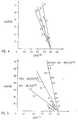
    Fig. 3 graphically illustrates the linear relationship between the magnetoresistive response as characterized by %ΔR/R of the spin valve sensor 10, relative to the square root of the absolute value of the electronegativity difference |Δχ|½ of the FM layers FM1, FM2 and the spacer 12, at room temperature, for a coupling field less than or equal to 10 Oersteds. This linear relationship is represented by a curve S1. It holds true for various spin valve layer compositions, and may be expressed generally by the following equation (3): (3) %ΔR/R ≅ A - B (|Δχ|)½, where A and B are constant values.
    It is generally recognized in the literature, for instance, Deny, "Giant Magnetoreristance in Spin-Valve Multilayers", Journal of Magnetism and Magnetic Materials, 136 (1994) 335-359 that a certain degree of roughness at the interface between the FM layers and the conductive spacers produces a maximal result (%ΔR/R) for a given interface. As the roughness increases or decreases from its optimal value %ΔR/R will decrease from its optimal value. This will reflect in a change in the slope, i.e., the constant value B in equation (3) above, but will not modify the proposed general principles offered by the invention, nor will it modify the
    We have determined that when spin valves and GMR sensors achieve the condition described by (|Δχ|)½ equal to 0.5 or greater than %ΔR/R =0, the following equation (4) related to the prior finding results in the following general relationship between %ΔR/R and |Δχ| as expressed below: %ΔR/R ≅ A - B (|Δχ|)½ , where (|Δχ|)½ = χ (FM) - χ (spacer); A ≅ B (|Δχ|)½; B ≅ 2A; and is a direct result of %ΔR/R = 0 when |Δχ|½ = 0.50 Thus %ΔR/R ≈ A - 2A (|Δχ|)½ = A{1 - 2 (|Δχ|)½}.
    In an exemplary embodiment of the spin valve sensor 10, the general equation (3) may be expressed by the following experimentally derived eq 5 for spin valves formed by a variety of interfaces equation (5): %ΔR/R = 35.20 - 70.40 (|Δχ|)½.
    Example 7
    Point D on curve S1 represents the following composition:Co - Cu - CO, where the first element (Co) is the unpinned FM layer FM1, the second element [Cu] is the conductive spacer 12, and the third element [Co] is the pinned FM layer FM2. Pursuant to equation (5), the composition of this example yields a %ΔR/R of approximately 9.5%.
    Example 8
    Point E on curve S1 represents Co - Cu - NiFe, where the first element Co is the unpinned FM layer FM1, the second element Cu is the conductive spacer 12, and the third element 80Ni-20Fe is the pinned FM layer FM2. Pursuant to equation (5), the composition of this example yields a %ΔR/R of approximately 6.5%.
    Example 9
    Point F on curve S1 represents [80Ni 20Fe]-[Cu]-[80Ni 20Fe], where the first element [80N-20Fe] is the unpinned FM layer FM1, the second element [Cu] is the conductive spacer 12, and the third element [80Ni 20Fe] is the pinned FM layer FM2. Pursuant to equation (5), the composition of this example yields a %ΔR/R of approximately 5%.
    Example 10
    Point G on curve S1 represents Co - Au - NiFe, where the first element Co is the unpinned FM layer FM1, the second element Au is the conductive spacer 12, and the third element 80Ni-20Fe is the pinned FM layer FM2. Pursuant to equation (5), the composition of this example yields a %ΔR/R of approximately 4.5%.
    Example 11
    Point H on curve S1 represents Ni- Cu -Ni, where the first element (Ni) is the unpinned FM layer FM1, the second element [Cu] is the conductive spacer 12, and the third element [Ni] is the pinned FM layer FM2. Pursuant to equation (5), the composition of this example yields a %ΔR/R of approximately 2.5%.
    Example 12
    Point I on curve S1 represents [80Ni 20Fe]-[Pt]-[80Ni 20Fe], where the first element [80Ni 20Fe] is the unpinned FM layer FM1, the second element [Pt] is the conductive spacer 12, and the third element [80Ni 20Fe] is the pinned FM layer FM2. Pursuant to equation (5), the composition of this example yields a %ΔR/R of approximately 0.3%.
    Example 13
    Point J on curve S1 represents [80Ni 20Fe]-[Pd]-[80Ni 20Fe], where the first element 80Ni 20Fe is the unpinned FM layer FM1, the second element [Pd] is the conductive spacer 12, and the third element 80Ni 20Fe is the pinned FM layer FM2. Pursuant to equation (5), the composition of this example yields a %ΔR/R of approximately 0.2%.
    Example 14
    Point K on curve S1 represents [80Ni 20Fe]-[Al]-[80Ni 20Fe], where the first element [80Ni 20Fe] is the unpinned FM layer FM1, the second element [Al] is the conductive spacer 12, and the third element [80Ni 20 Fe] is the pinned FM layer FM2. The square root of the electronegativity difference |Δχ|1/2 between Al and its adjacent NiFe layer FM1 is approximately 0.6/eV, which is greater than the intercept point value of 0.5 eV. In this and other similar examples where |Δχ|1/2 is greater than 0.5 eV, i.e., greater than the intercept point, then %ΔR/R is set equal to zero. This example further illustrates that the latter statement is true regardless of whether the crystallographic structures of adjacent layers are matched, i.e., 80Ni 20Fe and Al have FCC structures. The present teachings submit that Al may be useful if its electronegativity is matched with that of an appropriate ferromagnetic material.
    While the relationships described in the equations above, between the sensor output signals (%ΔR/R) and the absolute difference in electronegativities |Δχ|'s of adjacent layers has been described in view of data obtained at room temperature, further analyses confirm that these relationships are also valid for data obtained at other temperatures, including the sensor normal operating temperatures and at cryogenic temperatures as well. It should however be noted that, as shown in Fig. 4, the slope of the curve S1, i.e., the constant value A, will vary at different temperatures.
    The following examples 15 through 17 are made with reference to Fig. 4 which graphically illustrates the linear relationships between the %ΔR/R of the spin valve sensor 10 (Fig. 1) relative to the square root of the absolute value of the electronegativity difference (|Δχ|½ of the average electronegativity of the pinned and unpinned FM layers FM1 and FM2 and the spacer 12. The response is shown at three different measurement temperatures, that is, 300°K, 200°K and 100°K.
    Prior to the development of the relationship of the form of equations (3) and (4), no known quantitative method to maximize %ΔR/R was available in the prior art. By using equation (4) it is now possible to rationalize the selection of the materials forming the FM layers and are the conductive spacers, thus substantially minimizing the need for conventional trial and error selection processes. Consequently, the selection process can now be automated and/or rationalized, and significant cost savings can be achieved in the development of superior spin valve and GMR sensors. More particularly, an appropriate selection of materials can significantly improve the signal output of the spin valve sensor 10, which is a result that is highly sought and of great commercial value.
    The following examples are added for the purpose of illustration and explanation only. They are not intended to be exclusive or to limit the coverage of the present inventive concepts, including the selection process and the sensors. The values in these examples represent measurements at room temperature and lower temperatures as well.
    Example 15
    This example is represented by the curve V1 of Fig. 4 and graphically plots the linear relationship at a measurement temperature of 100 °K. Points "a", "b" and "c" reflect data for the following respective compositions:
  • The unpinned FM layer FM1:
       Co (point a), 80Ni 20Fe (point b), and Ni (point c),
  • The pinned FM layer FM2: {80Ni 20Fe].
  • The conductive spacer 12: Cu with a approximate thickness of 22A.
  • The χ values used for the FM layers are the average of pinned and free layers, χfree + χpinned.
    Example 16
    This example is represented by the curve V2 and graphically plots the linear relationship at a temperature of 200 °K. Points "d", "e" and "f" reflect data reported for similar compositions as in Example 15 above.
    Example 17
    This example is represented by the curve V3 and graphically plots the linear relationship at a temperature of 300 °K. Points "g", "h" and "i" reflect data reported for similar compositions as in Examples 15 and 16 above.
    For spin valve structures, the conductive spacer separating the FMs is generally between 18A° and 30° thick, while the FMs generally range between 30A° and 120A° with an optimum thickness typically at 60A° each. Fig. 5 graphically illustrates linear relationships between %ΔR/R of the GMR sensor 20 (Fig. 2) relative to the square root of the electronegativity difference |Δχ|½ of the FM layers FM and the spacers 22. %ΔR/R was measured at room temperature, for various cobalt nickel alloys. The resulting linear relationships are represented by three exemplary curves G1, G2, G3, and hold true for various GMR FM layer compositions. The curves G1, G2, G3 may be expressed generally by the following equations (6), (7) and (8), that continue to confirm equations (3) and (4).
    Curve G1 may be expressed by the following equation (6), and relates to the GMR first peak at a Cu thickness of approximately 10A: %ΔR/R ≅ 245 - 490 |Δχ|½.
    Curve G2 may be expressed by the following equation (7), and relates to the second GMR peak at a Cu thickness of approximately 22A: (7) %ΔR/R ≅ 110 - 220 |Δχ|½.
    Curve G3 may be expressed by the following equation (8), and represents the third GMR peak at a Cu thickness of approximately 32A to 36A: %ΔR/R ≅ 45 - 90 |Δχ|½.
    While only three peaks are illustrated, it should be clear that other peaks can also be used, i.e., the 4th or 5th Cu thickness at each of the first through fourth (or subsequent) peaks increases progressively to some optimal value, maximizing %ΔR/R for each particular peak. Increasing peak number or spacer thickness results in the switching field (ie., the field required to express the maximum %ΔR/R) at that particular peak to progressively decrease to lower values, and the sensitivity (ie., %ΔR/R per Oersted) to increase. Depending on the particular application, it is possible to select any of the GMR peaks. Additionally in GMR structures the FMs mcy range in thickness from 4A° to 25A°
    By using equations (3) and (6), (7) and (8) it is now possible to simplify the selection of the materials forming the various FM layers and conductive spacers 22 of the GMR sensor 20, similarly to what has been explained above in relation to the spin valve sensor 10.
    In addition, the following exemplary embodiments show that by a proper selection of the composition of the materials forming the sensor 20, and by matching or substantially minimizing the absolute electronegativity difference (or mismatch) of its layers (FM and conductive spacer), it is possible to obtain significantly higher output signals (%ΔR/R) than those attained so far using prior methods. The foregoing linear relationships were mostly obtained using data at room temperature. Further analyses confirm that these relationships are also valid for data obtained or derived at other temperatures, including the sensor normal operating temperatures of approximately 45°C and cryogenic temperatures as well. It should be noted that the slopes of the curve G1, G2, G3, i.e., the constant value B, will vary at different temperatures.
    An important finding of the present invention may be derived from equations (6), (7) and (8) namely that all the curves G1, G2 and G3 converge at a single intercept point (I), at which %ΔR/R = 0, when |Δχ|½ ≅ 0.5, regardless of the measurement temperatures and material compositions of the layers.
    The present analysis recognizes the need for optimizing the roughness of the interface for maximizing %ΔR/R for any particular interface. Accordingly, the curves G1, G2, G3 take into consideration the fact that different experimenters may conduct their experiments under different conditions, such as different substrate temperatures, different deposition rates, different Argon background sputtering pressure, and thus will realize different degrees of interfacial roughness. Again we reiterate that the interfacial surface roughness will vary the slopes of curves G1, G2 and G3 and that some optimum roughness exists that maximizes %ΔR/R for any interface Δχ of the FM and spacer layers.
    Example 18
    Fig. 5 shows the value of %ΔR/R for a GMR structure at three peaks as a function of NiCo alloy compositions.
  • Point H1 represents the composition: Ni30-Co70
  • Point J1 represents the composition: Co
  • Point L1 represents the composition: Ni50-Co50
  • Point M1 represents the composition: Ni70-Co30
  • Point N1 represents the composition: Ni80-Co20
  • Point P1 represents the composition: Ni90-Co10
  • Point Q1 represents the composition: Ni
  • All compositions of previous examples and this example 18 are given in Atomic %
    Example 19
    On the second GMR peak curve G2, points R1 and S1 correspond to the respective compositions of points J1, H1, and M1 along the first peak curve G1. R1 is Ni50-Co50; S1 is Ni70-Co30; T1 is Ni80-Co20; and U1 is Ni.
    Example 20
    On the third GMR peak curve G3, V1 is Ni30-Co70; W1 is Ni50-Co50; X1 is Ni70-Co30; and Y1 is Ni.
    Fig. 6 graphically illustrates three linear relationships between %ΔR/R of the GMR sensor 20 (Fig. 2) relative to the square root of the electronegativity difference |Δχ|½ of the FM layers FM and the spacers 22 at a temperature of 5 °K. These linear relationships are represented by three exemplary curves R1, R2, R3.
    Curve R1 may be expressed by the following equation (9), and relates to the GMR first peak: %ΔR/R ≅ 330 - 660 |Δχ|½
    Curve R2 may be expressed by the following equation (10), and relates to the second GMR peak: (10) %ΔR/R ≅ 158 - 316 (|Δχ|)½.
    Curve R3 may be expressed by the following equation (11), and relates to the third GMR peak: %ΔR/R ≅ 118 - 236 (|Δχ|)½.
    Example 21
    On the first GMR peak curve R1, the exemplary compositions are expressed as follows X-Y, where element X represents the material for the FM layers FM, and element "Y" represents the material for the conductive spacers 22.
  • Point g1 represents the following composition: Fe/Cr.
  • Point i1 represents the following composition: Co/Cu.
  • Point j1 represents the following composition: Co/Ag.
  • Example 22
    On the second GMR peak curve R2, points k1 and l1 correspond to the respective compositions of points i1 (Co/Cu), and j1 (Co/Ag) along the first peak curve G1.
    Example 23
    On the third GMR peak curve R3, points m1 and n1 correspond to the respective compositions of points i1 (Co/Cu), and j1 (Co/Ag) along the first peak curve G1.
    The foregoing example 1 through 21 confirms that the FCC and BCC systems obey the same or substantially similar principle as expressed by equations 3 and 4. Additionally it is shown that an FCC FM layer should be matched with an FCC conductive spacer, and a BCC FM layer should be matched with an BCC conductive spacer. For instance, when this lattice type matching, i.e., FCC on FCC and BCC on BCC ferromagnets and spacers, equations 3 and 4 are obeyed, relative to point "g" in example 1 above, both Fe and Cr are BCC elements, while the remaining exemplary points "h" through "j" relate to FCC conductors and ferromagnets.
    Point "p" relates to the GMR structure Fe - Cu. This structure presents an almost perfect electronegativity match i. e., (Δχ ≈ 0) between the Fe and Cu layers, nonetheless, this structure does not provide a high %ΔR/R since Fe is a BCC element, while Cu is a FCC element. Accordingly extremely inferior %ΔR/R is obtained and equations (3 and 4) are not obeyed due to potential barriers created by the lattice type mismatch, that is, BCC/FCC.
    The foregoing examples also confirm that the BCC and FCC systems are also similarly governed by the interfacial electronegativity matching principle, i.e., they have the same functionality of |Δχ|1/2 verses %ΔR/R as expressed by equations (3) and (4) and shown by example 21.
    Fig. 7 is a chart that graphically illustrates various exemplary combinations and compositions for the FM layers and spacers, some of which are explained by the following examples. In general, the FM alloys are selected from a group comprised of Fe, Co, Ni, and their alloys and substitutional alloys thereof. In addition, the conductive alloys are selected from a group comprised of Au, Cu, Ag and substitutional alloys thereof, and other suitable intermetalic compounds possessing resistivities
    Example 24
    Fig. 8 shows two graphs SL1, SL2, plotting the electrical resistivity in micro Ohmcm versus the atomic composition for the Cu-Au superlattice system. Graph SL1 illustrates the relationship for alloys that are quenched (disordered state). Graph SL2 illustrates the relationship for alloys that are annealed at 200°C for the purpose of rendering an ordered superlattice structure. Fig. 8 further shows that the specific electrical resistivities (microohm-cm) of the ordered superlattice relative to the same composition of the disordered alloy may be reduced significantly by annealing the alloys at predetermined atomic compositions. In the Cu-Au system exemplified in Fig. 8, two such predetermined atomic compositions are shown, the first (CP1) at 25 atomic percent of Au, and the second (CP2) at 50 atomic percent of Au. For the purpose of explanation, these atomic compositions at which the specific electrical resistivities of the alloys drop to a minimal level and the superlattice is formed, will be referred to herein as "critical points" (CP). Additional discription of superlattice structures may be found in C. Barrett, Ph.D.,"Structure of Metals, Crystallographic Methods, Principles, and Data", McGraw-Hill Book Company, Inc. (1952), second edition, 269-296, which is incorporated herein by reference.
    Example 25
    Fig. 9 shows two graphs SL3, SL4, plotting the electrical resistivity in micro ohmcm versus the atomic composition for the Cu-Pt superlattice system. Graph SL3 illustrates the relationship for alloys that are quenched and cold worked (disordered state). Graph SL4 illustrates the relationship for alloys that are annealed at 300°C for rendering an ordered superlattice structure. Fig. 9 further shows that the specific electrical resistivities of the ordered superlattice may be reduced significantly by annealing the alloys at two critical points CP3 (25% atomic percent Pt), and CP4 (50% atomic percent Pt).
    While points CP1 and CP2 (Fig. 8) and CP3, CP4 (Fig. 9) reflect the most useful compositions, other compositions defined by the hatched areas A1 (Fig. 8) and B1, B2 (Fig. 9) between the envelopes of the disordered alloys (SL1, SL3) and the envelopes of the ordered alloys (SL2, SL4) may also be useful in providing a broader electronegativity selection range, while at the same time producing a partially ordered superlattice that will have some benefit in extending the thermal stability of spin valve and GMR sensors using the ordered alloys.
    For example, the two alloy series in examples 24 and 25 may be annealed at between 120 °C to 250 °C in thin film form for approximately 0.5 hour to 4 hours to form the superlattice at appropriate composition. The present invention proposes the use of superlattices processed at or near critical points CP or within any of the shaded regions in the CuAu binary systemor the CuPtbinary system. The shaded regions define the composition range within which some degree of superlattice order will occur and which may be used advantageously. Clearly the most advantageous compositions from a resistivity point of view are a 25 and 50 atomic % for both the CuAu and CuPt. These superlattice alloys and compositions can be utilized to match the electronegativeity of 80Ni-20Fe, for example, more advantageously. The benefits are shown in the following examples. Similar superlattice alloys in the AgPd ssystem may be used to advantage as well. These are Cu3Pd or CuPd.
    Example 26
    A superlattice spacer 22 will provide a large mean free path in the spacer while simultaneously minimizing the electronegativity difference |Δχ| between the FM layers and the superlattice spacers 22. For example, 50:50 CuAu superlattice alloy (Fig. 9) exhibits a resistivity of about 3.5 µΩ-cm, which is similar to the resistivity of gold, and an average electronegativity (χ) of approximately 2.07 eV.
    In this example Permalloy (Ni80 - Fe20) is used as a FM layer. The electronegativity of 80:20 NiFe is about 2.095 eV and the electronegativity of the 50:50 CuAu superlattice alloy is approximately 2.07 eV, resulting in an absolute electronegativity difference |Δχ| of about 0.025 eV. This excellent match will significantly minimize the detrimental interfacial scattering component in the spin valve sensor 10 and the GMR sensor 20, with a result of maximizing sensor signal output %ΔR/R.
    Example 27
    In this example, the 50:50 CuAu superlattice alloy of Example 24 is used as a spacer, while cobalt (Co) is used as a FM layer. Since the electronegativity of Co is about 2.05 eV and the electronegativity of the 50:50 CuAu superlattice alloy is approximately 2.07 eV, thus resulting in an absolute electronegativity difference Δχ of 0.02, which provides a superior electronegativity match.
    Example 28
    In this example, a 50:50 CuAu superlattice (Figure 5) is used as a spacer, while an Ni3Fe superlattice composition forms the FM layers. The average electronegativity of the 50:50 CuAu superlattice is about 2.07, which has an absolute electronegativeity difference of about 0.01 with N13Fe.
    In addition to increasing the sensor output signals (%ΔR/R), the dual superlattice structure increases the thermal stability as well as the chemical stability of the sensors 10, 20. For instance, since the superlattice alloys are greatly more corrosion resistant than copper and the ferromagnet alloys, the sensors 10, 20 using the superlattices formed at or near critical points result in a structure of superior electromigration characteristics as well.
    As mentioned earlier, one method for processing the superlattice is to anneal the alloys between 120°C to 250°C for 10 to 200 minutes. An alternative method is to deposit the superlattice alloys by sputtering or evaporation, at a relatively low rate, on a sufficiently heated substrate. This slow deposition process could form the superlattice structure without the need for annealing.
    Another advantage for using superlattice structures is that such structures have high critical temperatures above which they become disordered. These critical temperatures exceed 350°C in bulk, that is well above the normal operating temperatures of the sensors 10, 20.
    The alloys that are used to achieve the preceding objectives are from the group constituting Fe, Ni, Co or any combination of these elements, and alloys thereof which, may be alloyeed with elements or combination thereof from the group consisting of Au, Cu, Mn, Ti, V, Pt, Pd, Ru, Ir, Sn, Ta, Nb, Rh, N, C, Zr, Hf, Y, La, and rare earth elements, either in crystalline FCC or BCC form or in amorphous form containing a combination of the above elements.
    Example 28
    Specifically, a group of quaternary FM alloys with minimal magnetostriction includes: [48Co - 29Ni - 23Fe] 1-yPd. [26Co - 44Ni - 30Fe] 1-yPd. In the foregoing two alloys, y represents the atomic fraction, and for (12 to 30)Pd, these alloys display near zero magnetostriction and low overcivity. More specifically, the following alloys have near zero magnetostriction and have χ values of 2.13. Each alloy can be matched with the superlattice composite conductive spacer of CuPt
    whose χ is approximately 2.12. 33.6Co - 20.3Ni - 16.1Fe - 30Pd. 18.2Co - 30.8Ni - 21Fe - 30Pd.
    The electronegativity matching between adjacent layers, as described in the foregoing equations may be carried out on a face-to-face or surface-to-surface basis. Fig. 10 illustrates the use of single crystals in the spin valve sensor 10 of Fig. 1. In this particular example the surface crystalline orientation of the substrate has been selected to be 111. As a result, the subsequent single crystal layers that are formed on top of the substrate will automatically assume the same 111 surface orientation. It is an object of the present invention to match the electronegativities of the selected crystalline orientation or face, which in this example is 111, of the juxtaposed layers, rather than to match the average electronegativities of these layers.
    According to a preferred embodiment, the spin valve sensor 10 is formed by selecting the desired spacer material and one of its three main crystalline orientations, for instance 111. Subsequently, the FM layers FM are selected such that the electronegativity of their corresponding faces with a 111 crystalline orientation matches or substantially approximates the electronegativity of the selected spacer crystalline face, i.e., 111. Similarly, the 110 and 100 surface faces can be matched as well by selecting the proper alloys. All examples up to this point were directed to polycrystalline ferromagnets and conductive spacers wherein the orientation of the individual crystallographic faces, i.e., 111, 100 and 110 are all present at about the same frequency of occurence. Given that the faces are equally presented to a grainy surface during the fabrication of spin valve or GMR sensors, the relevant electronegativeity of this random orientating crystallographic face is expressed by equation (12) wherein χs' of each principal face, i.e., 111, 100 and 110 contribute equally to the polycrystalline χ. χ(polycrystalline) = 1/3 (χ111 + χ100 + χ110) where n is an integer that is equal to 3 and representing the three main faces, and χi refers to the electronegativity of each of the three main faces.
    Fig. 11 illustrates the use of polycrystals in the spin valve sensor 10 of Fig. 1. In this particular example, the crystalline orientation of the substrate is random, and therefore the three main crystallographic orientations, i.e., 100, 110, 111 have approximately the same frequency of surface occupancy on the substrate. As a result, the subsequent polycrystal layers FM and AFM that are formed on top of the substrate will automatically assume the same random orientation as the substrate by epitaxy of the underlying polycrystals of the prior spacer or FM layer FM. It is an object of the present invention to match the average electronegativity of each layer to the average electronegativity of the adjacent layers.
    According to a preferred embodiment, the spin valve sensor 10 is formed by selecting the desired spacer material. Subsequently, the FM layers FM1 and FM2 are selected such that their average electronegativities match or substantially approximate the average electronegativity of the selected spacer 12.
    The following example 29 illustrates the impact of the mismatch of the electronegativity (|Δχ|) on the various faces 100, 110, 111 of polycrystalline nickel and polycrystalline copper.
    Example 29
    The electronegativity values and the electronegativity difference for the three faces of copper and nickel are listed in the following table:
    Cu (face) χCu (face) Ni (face) χ Ni (face) |Δχ|1/2 (face) for a spin valve
    Cu(111) 2.041 Ni (111) 2.204 0.40
    Cu(100) 1.87 Ni(100) 2.146 0.525
    Cu(110) 1.821 Ni(110) 2.068 0.498
    Applying equation (5) above, we can illustrate the impact on %ΔR/R as a function of the face, assuming equal surface occupancy of each principal face: %ΔR/R = 1/3 { [35.20-70.40(0.404)]111 + [35.20-70.40(0.525)]100 + [35.20-70.40(0.498)]110} %.
    In this equation, if |Δχ|1/2 ≥ 0.5 then |Δχ|1/2 is set equal to zero, and thus: %ΔR/R = 1/3 (6.758 + 0 + 0.14)% ≅ 2.30%, which value is close enough to the experimentally observed value of 2.5%, thus indicating that there is some probable preferred orientation and the sample was not completely random. The point to be illustrated is that essentially one face, in this example the face with the 111 surface orientation, contributes over approximately 90% of the %ΔR/R of the observed value, and thus emphasizes the necessity for matching the electronegativity on a single crystallographic face of the FM layer and the spacer for optimal %ΔR/R. By implementing this observation it is possible to triple %ΔR/R. The same observation applies to GMR structures as well.
    Figs. 12 and 13 illustrate a spin valve sensor 10A and a GMR sensor 20A respectively. The spin valve sensor 10A includes two or more compound FM interfaces (FM1, FM2) and (FM3, FM4) which are composed of different ferromagnetic materials. Similarly, the GMR sensor 20A includes a plurality of electrically conductive spacers, such as SPACER 1, that is interposed between, and interface with compound FM layers, such as (FM1, FM2), (FM3, FM4, FM5), (FM6, FM7). These compound interfaces follow similar rules to those of the coumpounds interfaces (FM1, FM2) and (FM3, FM4) of Fig. 12. In a preferred embodiment, all the interfaces between the FM layers (FM1, FM2, FM3, FM4 and spacer follow the electronegativity matching and other selection criteria described herein. In addition, the counpound interfaces enable the adjustment of the overall magnetostriction for the spin valve sensor 10A and the GMR sensor 20A. For the structures of Fig. 12 (spin valve) and Fig. 13, GMR FM1 and FM4 may be identical compositions, or may be different compositions, and the same applies to FM2 and FM3. While in the preferred embodiment, FM2 and FM3 are of the same composition, FM1 and FM4 are of the same composition as well. The basis for having two or more different compositions is that the magnetostriction thickness product of FM1 and F2 may be arranged so that +λstFM1 _ -λstFM2, where t is thickness, resulting in an average λs (magnetostriction) for both layers approaching zero for the composite FM elements.
    It is not necessary to match thicknesses of FM1 and FM2, or FM3 and FM4, to minizize magnetostriction. Even an unbalanced thickness of each will lower λs for improved results that minimizes magnetostriction of a compound FM structure. What is critical is that the ferromagnets immediately adjacent to the spacers minimize their Δχ relative to the chosen spacer. Entirely similar conditions prevail for the GMR structure of Fig. 13 as well. Thus, the compound FM structure in spin valve structures and GMR structures, in combination with the preceding teaching requiring the minimization of Δχ between FM and spacer, allows for maximizing %ΔR/R while simultaneously maximizing corrosion resistance and minimizing the magnetostriction of compound ferromagnet structures of spin valve structures or GMR structures.
    In the above example, it was demonstrated in the Ni-Cu multilayer system that ≈90 + % of %ΔR/R was due to crystallites comprising the multilayer spin valve that were in the 111 surface orientation. It is well known that even in polycrystalline films with random surface orientations of 111, 100 and 110 planes that epitaxy of the succeeding Cu and FM films will occur, i.e., the orientation effect is carried throughout the structure.
    EXAMPLE 30
    The selection of crystal orientation, 111, 100 or 110 can be accomplished by selecting a single crystal substrate such as single crystal magnesium oxide with surface orientations of either 111, 100 or 110. By selecting a single orientation, for example 111 of
    the substrate and subsequently selecting a ferromagnet and conductive spacer whose Δχ's are minimized, and subsequently depositing alternating layers of FM and conductive spacers on such an oriented substrate, results in %ΔR/R's that will be greater than randomly oriented polycrystalline structures.
    Prior to the deposition of alternating ferromagnets and spacers, it would be desirable to deposit a first layer of Pt, Pd, Au or Cr of 10 Å to 50 Å with subsequent annealing at approximately 250-400°C to establish an epitaxial oriented metal film from which subsequent epitaxy of the selected alternating FM/spacer materials are then subsequently deposited with epitoxialintegrity maintained at each subsequent layer in the formation of a spin valve or GMR structure.
    Since interfacial diffusion kinetics between the FM and the conductor spacer are expected to be a function of selected orientation, that is, 111, 100 or 110, the surface roughness of each selected orientation is optimized by optimizing the deposition conditions for each orientation. In this way, a maximum %ΔR/R can be achieved for each principal orientation, 111, 100 or 110.
    Since no χ or Ø values are found in the literature for alloys, we estimate the 111, 100, 110 χvalues of the polycrystalline value of the alloy for whichthe method of calculation has been shown. By using FCC elements such as Ni, Al, Ag, Ir, CU, and their polycrystalline χ values and noting the ratio of the above elements to the polycrystalline value, we can arrive at an estimate of the 111, 100, 110 χ values for any arbitrary FCC alloy. The result is as follows, where χpc = χpolycrystalline: χ111 _ 1.027 χPC χ100 _ 1.007 χPC χ110 _ 0.965 χPC
    Accordingly, these estimates provide a basis for matching single crystal orientations of the FM alloy with single crystal orienatations of the conductive spacers for the purpose of minimizing Δχ.
    EXAMPLE 31
    Heusler alloys represent another class of ferromagnetic materials possessing a superlattice structure that may be partially or fully ordered. Full ordering is possible at or very near to the general stoichiometric composition M2MnM1 and may contain ferromagnetic elements Co and Ni for M2 as well as the nonferromagnetic elements Cu, Pd, Pt and Au; whereas M1 may be Al, Ga, As, In, Sb, Sn or Bi. The Heusler alloys containing full complements of Pt, Au, Pd have Curie temperatures below room temperatures, i.e., below 300°K and accordingly may, if their resistivity ≤ 20 microohm cm., be used as spacers for other ferromagnetic Heusler alloys. It is also possible to admix for M2, Cu, Co, Ni, Pd, Pt, Au and Ir for the purpose of fine control of the electronegativity of the Heusler alloy to minimize Δχ of the Heusler alloy and its spacer element or alloy or compound.
    A representative series of Heusler alloys and their electronegativities is illustrated below:
    Heusler Alloy χalloy
    Cu2MnAl 1.80
    Ni2MnSn 1.93
    Co2MnGe 1.94
    Co2MnSi 1.93
    Co2MnSn 1.89
    CuPdMnSn 1.92
    NiAuMnSn 1.95
    The above ferromagnetic superlattice alloys may be used in conjunction with Cu, CuAu alloys, with Au at 5-15 atomic % and intermetallic spacers Al2Au with χ = 1.88 and PtAl2 whose χ = 1.92. AgAu alloys may be used as well with Au less than 25 atomic %.
    A list of χ values that are relevant to most ferromagnetic alloys and conductive spacer compounds or alloys is provided below:
    Element Polycrystalline χ Bulk Crystal Structure
    Au 2.22 FCC
    Fe 1.91 BCC
    Cu 1.91 FCC
    Ag 1.89 FCC
    Pt 2.34 FCC
    Pd 2.32 FCC
    Ir 2.32 FCC
    Rh 2.04 FCC
    Co 2.05 FCC in thin films
    Ni 2.14 FCC
    Mn 1.65 Complex
    Cr 1.83 BCC
    Ti 1.76
    V 1.74 BCC
    Ru 1.92 CPH close packed hexagonal
    Sn 1.79 Complex
    Ta 1.73 BCC
    Nb 1.75 BCC
    Zr 1.63 BCC CPH
    Hf 1.57 CPH
    Y 1.21 CPH
    La 1.39 FCC CPH
    Rare earth elements 1.21 Complex CPH FCC BCC
    C 2.52 Various forms
    N 3.01 Gaseous
    Al 1.72 FCC
    Ge 2.00
    Si 1.96
    Bi 1.71
    As 1.50
    By virtue of this invention, a method and means has been provided for selecting the materials of spin valve and GMR sensors to yield minimal difference in electronegativity between the sensor layers.

    Claims (54)

    1. A method of making sensors (10) formed with ferromagnetic layers (FM1, FM2), and conductive spacers (12) interposed between the ferromagnetic layers (FM1, FM2), for use in data storage devices, comprising the steps of:
      selecting a first material of either said ferromagnetic layers (FM1, FM2) or said electrically conductive spacers (12) having a first electronegativity; and
      selecting a second material for said other nonselected one of said ferromagnetic layers (FM1, FM2) and said conductive spacers (12) having a second electronegativity;
      wherein the absolute difference between said first and second electronegativities is minimized.
    2. The method as in claim 1, wherein said ferromagnetic layers (FM1, FM2) comprise a plurality of layers having a plurality of different electronegativities.
    3. The method as in claim 1 or 2, wherein said step of selecting said electrically conductive spacer material includes the step of selecting material from the group comprising Cu, Ag, Au, Pt, Pd, Cu3Pt, CuPt, Cu3Au, CuAu and Cr.
    4. The method as in any one of the preceding claims, wherein said step of selecting said ferromagnetic layers (FM1, FM2) includes the step of selecting materials from the group comprising NiFe(80:20), Ni3Fe, Ni3Mn, Fe4Mn, FePd, Fe1-y Auy, Co1-z Auz, where y is the atomic fraction with a value between 0.30 and 0.70, and z is the atomic fraction with a value between 0.10 and 0.50.
    5. The method as in any one of the preceding claims, wherein said step of selecting said electrically conductive spacer (12) includes the step of selecting Cr. and wherein said step of selecting said ferromagnetic layers (FM1, FM2) includes the step of selecting ferromagnetic materials from the group comprising Fe1-v Crv, Fe1-w Vw, ternary FeCrV systems, where u is the atomic fraction with a value between 0.40 and 0.70, and w is the atomic fraction with a value between 0.25 and 0.35.
    6. The method as in any one of the preceding claims, wherein said step of selecting said electrically conductive spacer (12) includes the step of defining said at least first and second electronegativities according to the following equations: χ (spacer) = 0.44 (spacer) - 0.15, and χ (FM) = 0.44  (FM) - 0.15, where (spacer) and (FM) are the work functions of said electrically conductive spacer (12), and said ferromagnetic layers (FM1, FM2).
    7. The method as in claim 6, wherein the step of selecting said electrically conductive spacer (12) includes the step of selecting a binary conductive alloy(a-b) having an electronegativity χ and formed of a plurality of elements a and b, where said elements a and b have electronegativities χa and χb, and atomic fractions fa and fb, respectively; and
      wherein said electronegativity of said alloy χ is defined by the following equation: χ(alloy a-b) = χa.fa + χb. fb.
    8. The method as in claim 6, wherein the step of selecting said electrically conductive spacer (12) includes the step of selecting a ternary conductive alloy(a-b-c) having an electronegativity χ and formed of a plurality of elements a, b and c;
      wherein said elements a, b and c have electronegativities χa, χb and χb, and atomic fractions fa, fb and fc respectively; and
      wherein said electronegativity of said alloy χ is defined by the following equation: χ(alloy a-b-c) = χa.fa + χb. fb + χc. fc.
    9. The method as in claim 6, wherein the step of selecting said ferromagnetic layers (FM1, FM2) includes the step of selecting a binary ferromagnetic alloy(x-y) having an electronegativity χ and formed of a plurality of elements x and y;
      wherein said elements x and y have electronegativities χx and χy, and atomic fractions fx and fy respectively; and
      wherein said electronegativity of said alloy χ(alloy x-y) is defined by the following equation: χ(alloy x-y) = χx.fx + χy. fy.
    10. The method as in claim 6, wherein the step of selecting said ferromagnetic layers (FM1, FM2) includes the step of selecting a ternary ferromagnetic alloy(x-y-z) having an electronegativity χ and formed of a plurality of elements x, y and z;
      wherein said elements x, y and z have electronegativities χx, χy and χx and atomic fractions fx, fy and fz respectively; and
      wherein said electronegativity of said alloy χ(alloy x-y-z) is defined by the following equation: χ(alloy x-y-z) = χx.fx + χy. fy + χz. fz.
    11. A method of optimizing the interfacial properties of a data storage device comprising the steps of:
      selecting at least one electrically conductive spacer (12) having a first work function ( spacer); and
      selecting ferromagnetic layers (FM1, FM2) having at least a second work function ( FM);
      wherein said selecting steps include the step of matching said at least first and second work functions.
    12. A data storage device comprising:
      a substrate;
      at least one electrically conductive spacer (12) having a first electronegativity; and
      ferromagnetic layers (FM1, FM2) having a second electronegativity disposed adjacent to said conductive spacer (12);
      wherein said conductive spacer (12) and said ferromagnetic layers (FM1, FM2) are selected such that said first and second electronegativities are matched for optimizing the interfacial properties of the data storage device.
    13. The data storage device as in claim 12, wherein said first electronegativity corresponds to a first work function;
      wherein said second electronegativity corresponds to a second work function; and
      wherein said at least first and second work functions are matched for optimizing the interfacial properties of the data storage device.
    14. The data storage device of claim 12 or 13, wherein the difference between said first and second electronegativities is minimized according to the following equation: |Δχ| = χ (FM) - χ (spacer) ≈ 0.
    15. The data storage device as in any one of claims 12 to 14, wherein said first and second electronegativities are defined according to the following equations: χ (spacer) = 0.44 (spacer) - 0.15, and χ (FM) = 0.44  (FM) - 0.15, where (spacer) and (FM) are the work functions of said electrically conductive spacer (12), and said ferromagnetic layers (FM1, FM2).
    16. The data storage device as in any one of claims 12 to 15, wherein said electrically conductive spacer (12) includes a binary conductive alloy(a-b) having an electronegativity χ and formed of a plurality of elements a and b;
      wherein said elements a and b have electronegativities χa and χb, and atomic fractions fa and fb, respectively; and
      wherein said electronegativity of said alloy χ(alloy a-b)is defined by the following equation: χ(alloy a-b) = χa.fa + χb. fb.
    17. The data storage device as in any one of claims 12 to 15, wherein said electrically conductive spacer (12) includes a ternary conductive alloy(a-b-c) having an electronegativity χ and formed of a plurality of elements a, b and c;
      wherein said elements a, b and c have electronegativities χa, χb and χb, and atomic fractions fa, fb and fc respectively; and
      wherein said electronegativity of said alloy χ(alloy a-b-c) is defined by the following equation: χ(alloy a-b-c) = χa.fa + χb. fb + χc. fc.
    18. The data storage device as in any one of claims 12 to 15, wherein said ferromagnetic layers (FM1, FM2) include a binary ferromagnetic alloy(x-y) having an electronegativity χ and formed of a plurality of elements x and y;
      wherein said elements x and y have electronegativities χx and χy, and atomic fractions fx and fy respectively; and
      wherein said electronegativity of said alloy χ(alloy x-y) is defined by the following equation: χ(alloy x-y) = χx.fx + χy. fy.
    19. The data storage device as in any one of claims 12 to 15, wherein said ferromagnetic layers (FM1, FM2) include a ternary ferromagnetic alloy(x-y-z) having an electronegativity χ and formed of a plurality of elements x, y and z;
      wherein said elements x, y and z have electronegativities χx, χy and χx and atomic fractions fx, fy and fz respectively; and
      wherein said electronegativity of said alloy χ(alloy x-y-z) is defined by the following equation: χ(alloy x-y-z) = χx.fx + χy. fy + χz. fz .
    20. The data storage device as in any one of claims 12 to 15, wherein said conductive spacer (12) comprises a plurality of electrically conductive spacers (12) having a plurality of electronegativities;
      wherein said ferromagnetic layers (FM1, FM2) comprise a plurality of ferromagnetic layers (FM1, FM2) having a plurality of electronegativities; and
      wherein said electronegativities of said conductive spacers (12) are matched with said electronegativities of said ferromagnetic layers (FM1, FM2).
    21. The data storage device as in any one of claims 12 to 20, wherein said electrically conductive spacer (12) is selected from the group comprising Cu, Ag, Au, Pt, Pd, Cu3Pt, CuPt, Cu3Au, CuAu and Cr.
    22. The data storage device as in any one of claims 12 to 21, wherein said ferromagnetic layers (FM1, FM2) are selected from the group comprising NiFe(80:20), Ni3Fe, Ni3Mn, Fe4Mn, FePd, Fe1-y Auy, Co1-z Auz, where y is the atomic fraction with a value between 0.30 and 0.70, and z is the atomic fraction with a value between 0.10 and 0.50; or the group comprising Fe1-v Crv, Fe1-w Vw, ternary FeCrV systems, where u is the atomic fraction with a value between 0.40 and 0.70, and w is the atomic fraction with a value between 0.25 and 0.35.
    23. The data storage device as in any one of claims 12 to 22, wherein at least one of said ferromagnetic layers (FM1, FM2) defines a compound interface with said conductive spacer (12).
    24. A method of optimizing the interfacial properties of a data storage device comprising the steps of:
      selecting a substrate having a defined crystallographic structure;
      selecting at least one electrically conductive, single crystal spacer having a crystallographic structure similar to said substrate crystallographic structure and having a first electronegativity; and
      selecting ferromagnetic, single crystal layers having a crystallographic structure similar to said substrate crystallographic structure and having second electronegativity: wherein said selecting steps provide a matching of said at least first and second electronegativities.
    25. The method as in claim 24, wherein said step of selecting said substrate includes selecting a substrate material with a face centered cubic structure;
      wherein said step of selecting said single crystal spacer includes selecting a spacer material with a face centered cubic structure; and
      wherein said step of selecting said single crystal ferromagnetic layers (FM1, FM2) includes selecting a ferromagnetic layer material with a face centered cubic structure.
    26. The method as in claim 24 or 25, wherein said step of selecting a spacer with a face centered cubic structure includes the step of selecting said spacer from a group comprising Cu, Ag, Au, Pt, Pd, Cu3Pt, CuPt, Cu3Au, CuAu, AgPt3, Crlr3, Cr2Pt, AlCu3 and Al2Cu.
    27. The method as in any one of claims 24 to 26, wherein said step of selecting a ferromagnetic layer with a face centered cubic structure includes selecting said ferromagnetic layer from the groups comprising NiFe(80:20), Ni3Fe, Ni3Mn, Fe4Mn, FePd, Fe1-y Auy, Co1-z Auz, where y is the atomic fraction with a value between 0.30 and 0.70, and z is the atomic fraction with a value between 0.10 and 0.50; and Fe1-v Crv, Fe1-w Vw, ternary FeCrV systems, where u is the atomic fraction with a value between 0.40 and 0.70, and w is the atomic fraction with a value between 0.25 and 0.35.
    28. The method as in any one of claims 24 to 27, wherein said step of selecting said substrate includes selecting a substrate material with a base centered cubic structure;
      wherein said step of selecting said single crystal spacer includes selecting a spacer material with a base centered cubic structure; and
      wherein said step of selecting said single crystal ferromagnetic layers (FM1, FM2) includes selecting a ferromagnetic layer material with a base centered cubic structure.
    29. The method as in claim 28, wherein said step of selecting a conductive spacer (12) with a base centered cubic structure includes the step of selecting Cr.
    30. The method as in claim 28, wherein said step of selecting a ferromagnetic layer with a base centered cubic structure includes the step of selecting said ferromagnetic layer from the group comprising Cr, Fe, V, Mo, W, Nb and Ta.
    31. The method of any one of claims 24 to 30, wherein said step of substantially matching includes the step of minimizing the difference between said first and second electronegativities as in the following equation: |Δχ| = χ (FM) - χ (spacer) ≈ 0
    32. A method of optimizing the interfacial properties of a data storage device comprising the steps of:
      selecting a substrate having a defined crystallographic structure;
      selecting an electrically conductive, polycrystalline spacer having a plurality of individual crystallographic faces, each of said faces having an electronegativity, said spacer defining an average electronegativity; and
      selecting a polycrystalline ferromagnetic layer having a plurality of individual crystallographic faces corresponding to said crystallographic faces of said spacer, each of said faces having an electronegativity, said ferromagnetic layer defining an average electronegativity;
      wherein said selecting steps provide for matching said electronegativity of an individual crystallographic face of said spacer with said electronegativity of a corresponding individual crystallographic face of said ferromagnetic layer.
    33. A method of optimizing the interfacial properties of a data storage device comprising the steps of:
      selecting a substrate having a predetermined crystallographic structure;
      selecting an electrically conductive, polycrystalline spacer having a plurality of individual crystallographic faces, each of said faces having an electronegativity, said spacer defining an average electronegativity; and
      selecting a polycrystalline ferromagnetic layer having a plurality of individual crystallographic faces corresponding to said crystallographic faces of said spacer, each of said faces having an electronegativity, said ferromagnetic layer defining an average electronegativity;
      wherein said selecting steps provide for matching said average electronegativity of said spacer with said average electronegativity of said ferromagnetic layer.
    34. A method of optimizing the interfacial properties of a data storage device comprising the steps of:
      selecting a substrate having a predetermined crystallographic structure;
      selecting at least one electrically conductive, single crystal spacer having a crystallographic structure similar to said substrate crystallographic structure and having a first work function;
      selecting ferromagnetic, single crystal layers having a crystallographic structure similar to said substrate crystallographic structure and having a second work function; and
      wherein said selecting steps include the step of substantially matching said first and second work functions.
    35. A method of optimizing the interfacial properties of a data storage device comprising the steps of:
      selecting a substrate having a defined crystallographic structure;
      selecting an electrically conductive, polycrystalline spacer having a plurality of individual crystallographic faces, each of said faces having a work function, said spacer defining an average work function; and
      selecting a polycrystalline ferromagnetic layer having a plurality of individual crystallographic faces corresponding to said crystallographic faces of said spacer, each of said faces having a work function, said ferromagnetic layer defining an average work function;
      wherein said selecting steps include matching said average work function of said spacer with said average work function of said ferromagnetic layer.
    36. A data storage device comprising:
      a substrate having a defined crystallographic structure;
      at least one electrically conductive, single crystal spacer having a crystallographic structure similar to said substrate crystallographic structure and having a first electronegativity; and
      ferromagnetic, single crystal layers having a crystallographic structure similar to said substrate crystallographic structure and having a second electronegativity; and
      wherein said electrically conductive spacer (12) and said ferromagnetic layers (FM1, FM2) are selected so that said first and second electronegativities and are matched for optimizing the interfacial properties of the data storage device.
    37. A data storage device comprising in combination:
      a substrate having a predetermined crystallographic structure;
      an electrically conductive, polycrystalline spacer having a plurality of individual crystallographic faces, each of said faces having an electronegativity, said spacer defining an average electronegativity; and
      a polycrystalline ferromagnetic layer having a plurality of individual crystallographic faces corresponding to said crystallographic faces of said spacer, each of said faces having an electronegativity, said ferromagnetic layer defining an average electronegativity;
      wherein said spacer and said ferromagnetic layer are selected so that said average electronegativity of said spacer matches said average electronegativity of said ferromagnetic layer for optimizing the interfacial properties of the data storage device.
    38. A data storage device comprising:
      a substrate having a predetermined crystallographic structure;
      an electrically conductive, polycrystalline spacer having a plurality of individual crystallographic faces, each of said faces of said spacer having an electronegativity, said spacer defining an average electronegativity; and
      a polycrystalline ferromagnetic layer having a plurality of individual crystallographic faces corresponding to said crystallographic faces of said spacer, each of said faces of said polycrystalline ferromagnetic layer having an electronegativity, said ferromagnetic layer defining an average electronegativity; wherein said spacer and said ferromagnetic layer are selected so that the electronegativity of an individual crystallographic face of said spacer matches the electronegativity of an individual crystallographic face of said ferromagnetic layer for optimizing the interfacial properties of the data storage device.
    39. The data storage device as in claim 37 wherein said plurality of individual crystallographic faces of said spacer include three faces: 111, 110 and 100, having individual electronegativities χ111, χ100, and χ110, respectively; and
      wherein said average electronegativity of said spacer is defined by the following equation: χ(average- spacer) = 1/3 (χ111 + χ100 + χ110).
    40. The data storage device as in claim 37 wherein said plurality of individual crystallographic faces of said ferromagnetic layer includes three faces: 111, 110 and 100, having individual electronegativities χ111, χ100, and χ110, respectively; and
      wherein said average electronegativity of said ferromagnetic layer is defined by the following equation: χ(average- FM) = 1/3 (χ111 + χ100 + χ110).
    41. The data storage device as in claim 36 including a spin valve sensor formed of said substrate, said electrically conductive, single crystal spacer, and said ferromagnetic layers (FM1, FM2).
    42. The data storage device as in claim 16 including a giant magnetorsistance sensor (20) formed of said substrate, said electrically conductive, single crystal spacer, and said ferromagnetic layers (FM1, FM2).
    43. The method as in claim 1, wherein at least one of said ferromagnetic layers (FM1, FM2) is formed with said first material and said conductive spacer (12) is formed with said second material.
    44. The method as in claim 1, wherein said ferromagnetic layers (FM1, FM2) comprise a plurality of layers having different electronegativities.
    45. The method as in claim 1, wherein said conductive spacer (12) comprises a plurality of spacers (12) having different electronegativities.
    46. The method as in claim 45, wherein said sensor is a giant magnetorsistance sensor (20).
    47. A data storage device comprising in combination:
      a substrate;
      electrically conductive spacer (12) means formed on said substrate, said spacer having a first electronegativity; and
      ferromagnetic layer means formed adjacent to said spacer means (12) and having a second electronegativity;
      wherein a magnetoresistive response characteristic (%ΔR/R) of the data storage device is optimized by correlating said first and second electronegativities to %ΔR/R as follows: %ΔR/R ≅ A - B (|Δχ|)½, where A and B are constant values and |Δχ| is the absolute value of the difference between said first and second electronegativities.
    48. The data storage device as in claim 47, wherein said ferromagnetic layer means constitutes a plurality of ferromagnetic layers (FM1, FM2); and said conductive spacer (12) means comprises a number of spacer layers interposed between said ferromagnetic layers (FM1, FM2); and
      wherein the electronegativities of adjacent spacers (12) and ferromagnetic layers (FM1, FM2) are matched.
    49. A method of optimizing the magnetoresistive response (%ΔR/R) of a data storage device, comprising the steps of:
      selecting at least one electrically conductive spacer (12) having at least a first electronegativity; and
      selecting ferromagnetic layers (FM1, FM2) having at least a second electronegativity;
      wherein said selecting steps include correlating said first and second electronegativities for optimizing %ΔR/R in accordance with the following equation: %ΔR/R ≅ A - B (|Δχ|)½, where A and B are constant values and |Δχ| is the absolute value of the difference between said first and second electronegativities.
    50. The method according to claim 49, wherein said step of correlating includes the step of optimizing %ΔR/R in view of the following relationship: %ΔR/R ≅ A - 2A (|Δχ|)½.
    51. The method according to claim 50, wherein the data storage device includes a spin valve sensor, including the step of setting the constant value A equal to 35.20.
    52. The method according to claim 50, wherein the data storage device includes a giant magnetorsistance sensor (20) having a first peak, including the step of setting the constant value A equal to 300 for said first peak.
    53. The method according to claim 50, wherein the data storage device includes a giant magnetorsistance sensor (20) having first and second peaks, including the step of setting the constant value A equal to 110 for said second peak.
    54. The method according to claim 50, wherein the data storage device includes a giant magnetorsistance sensor (20) having first, second and third peaks, including the step of setting the constant value A equal to 45 for said third peak.
    EP97114191A 1996-08-26 1997-08-18 Methods and compositions for optimizing interfacial properties of transducers used in data storage devices Withdrawn EP0827220A3 (en)

    Applications Claiming Priority (2)

    Application Number Priority Date Filing Date Title
    US702977 1996-08-26
    US08/702,977 US5793279A (en) 1996-08-26 1996-08-26 Methods and compositions for optimizing interfacial properties of magnetoresistive sensors

    Publications (2)

    Publication Number Publication Date
    EP0827220A2 true EP0827220A2 (en) 1998-03-04
    EP0827220A3 EP0827220A3 (en) 1999-06-09

    Family

    ID=24823431

    Family Applications (2)

    Application Number Title Priority Date Filing Date
    EP97114191A Withdrawn EP0827220A3 (en) 1996-08-26 1997-08-18 Methods and compositions for optimizing interfacial properties of transducers used in data storage devices
    EP97114774A Withdrawn EP0827221A3 (en) 1996-08-26 1997-08-26 Methods and compositions for optimizing interfacial properties of magnetoresistive sensors

    Family Applications After (1)

    Application Number Title Priority Date Filing Date
    EP97114774A Withdrawn EP0827221A3 (en) 1996-08-26 1997-08-26 Methods and compositions for optimizing interfacial properties of magnetoresistive sensors

    Country Status (3)

    Country Link
    US (2) US5793279A (en)
    EP (2) EP0827220A3 (en)
    JP (1) JPH10177705A (en)

    Cited By (4)

    * Cited by examiner, † Cited by third party
    Publication number Priority date Publication date Assignee Title
    WO2003089946A1 (en) * 2002-04-18 2003-10-30 Seagate Technology Llc Gmr spin valve structure using heusler alloy
    EP1450177A2 (en) * 2003-02-24 2004-08-25 Hitachi Global Storage Technologies, Inc. Magnetoresistive device with exchange-coupled structure having half-metallic ferromagnetic Heusler alloy in the pinned layer
    GB2406962A (en) * 2003-10-06 2005-04-13 Alps Electric Co Ltd Magnetic Sensing Element
    US10971176B2 (en) 2019-02-21 2021-04-06 International Business Machines Corporation Tunnel magnetoresistive sensor with adjacent gap having chromium alloy seed layer and refractory material layer

    Families Citing this family (181)

    * Cited by examiner, † Cited by third party
    Publication number Priority date Publication date Assignee Title
    JP2748876B2 (en) * 1995-01-27 1998-05-13 日本電気株式会社 Magnetoresistive film
    US5793279A (en) * 1996-08-26 1998-08-11 Read-Rite Corporation Methods and compositions for optimizing interfacial properties of magnetoresistive sensors
    JP3827789B2 (en) * 1996-12-27 2006-09-27 株式会社東芝 Magnetoresistive head
    JP2950284B2 (en) * 1997-05-14 1999-09-20 日本電気株式会社 Magnetoresistive element, magnetoresistive sensor using the same, magnetoresistive detection system and magnetic storage system
    JP2985964B2 (en) * 1997-06-30 1999-12-06 日本電気株式会社 Magnetoresistive head and its initialization method
    JP2925542B1 (en) * 1998-03-12 1999-07-28 ティーディーケイ株式会社 Magnetoresistive film and magnetoresistive head
    JPH11354860A (en) * 1998-06-10 1999-12-24 Read Rite Smi Kk Spin valve magnetic conversion element and magnetic head
    US6166890A (en) * 1998-07-24 2000-12-26 Seagate Technology Llc In plane, push-pull parallel force microactuator
    CA2341857A1 (en) * 1998-08-28 2000-03-09 The Research Foundation Of The State University Of New York Magnetoresistive material with two metallic magnetic phases
    US6375761B1 (en) 1998-08-28 2002-04-23 The Research Foundation Of State University Of New York Magnetoresistive material with two metallic magnetic phases
    US6498707B1 (en) 1999-04-20 2002-12-24 Seagate Technology, Llc Giant magnetoresistive sensor with a CrMnPt pinning layer and a NiFeCr seed layer
    JP3331397B2 (en) * 1999-07-23 2002-10-07 ティーディーケイ株式会社 Tunnel magnetoresistive element
    US6308400B1 (en) * 1999-08-06 2001-10-30 Headway Technologies, Inc. Method for achieving anti-parallel exchange coupling with one biased layer having low coercivity
    US6456469B1 (en) 2000-06-05 2002-09-24 International Business Machines Corporation Buffer layer of a spin valve structure
    US6515573B1 (en) * 2000-06-19 2003-02-04 Read-Rite Corporation Method and system for providing edge-junction TMR utilizing a hard magnet as a pinned layer
    US6982854B2 (en) * 2000-06-22 2006-01-03 Matsushita Electric Industrial Co., Ltd. Magnetoresistance effect device and magnetoresistance effect head comprising the same, and magnetic recording/reproducing apparatus
    US6563680B2 (en) 2001-03-08 2003-05-13 International Business Machines Corporation Spin valve sensor with pinned layer and antiparallel (AP) pinned layer structure pinned by a single pinning layer
    US6665155B2 (en) 2001-03-08 2003-12-16 International Business Machines Corporation Spin valve sensor with free layer structure having a cobalt niobium (CoNb) or cobalt niobium hafnium (CoNbHf) layer
    US6700754B2 (en) 2001-04-30 2004-03-02 International Business Machines Corporation Oxidized copper (Cu) spacer between free and pinned layer for high performance spin valve applications
    US6954342B2 (en) * 2001-04-30 2005-10-11 Hitachi Global Storage Technologies Netherlands B.V. Underlayer for high amplitude spin valve sensors
    US6628484B2 (en) * 2001-06-05 2003-09-30 International Business Machines Corporation Planar gap pre-fill process for read heads
    US6600638B2 (en) 2001-09-17 2003-07-29 International Business Machines Corporation Corrosion resistive GMR and MTJ sensors
    JP3607678B2 (en) * 2002-01-24 2005-01-05 アルプス電気株式会社 Magnetic detection element
    US7028743B1 (en) * 2002-06-28 2006-04-18 Seagate Technology Llc High field contrast magnetic stampers/imprinters for contact patterning of magnetic media
    JP4487472B2 (en) * 2002-07-05 2010-06-23 株式会社日立製作所 Magnetoresistive element, magnetic head including the same, magnetic recording apparatus, and magnetic memory
    US6952364B2 (en) 2003-03-03 2005-10-04 Samsung Electronics Co., Ltd. Magnetic tunnel junction structures and methods of fabrication
    US6993827B2 (en) * 2003-06-12 2006-02-07 Headway Technologies, Inc. Method of making a bottom spin valve
    US7207098B2 (en) * 2003-06-27 2007-04-24 Seagate Technology Llc Hard mask method of forming a reader of a magnetic head
    JP2005116703A (en) * 2003-10-06 2005-04-28 Alps Electric Co Ltd Magnetic detecting element
    KR100624417B1 (en) * 2004-01-31 2006-09-18 삼성전자주식회사 Tunneling Magnetoresisance Device
    JP4904499B2 (en) * 2004-09-06 2012-03-28 国立大学法人 鹿児島大学 Spintronic materials and TMR elements
    JP4179260B2 (en) * 2004-09-29 2008-11-12 ソニー株式会社 Magnetoresistive magnetic head and magnetic tape device
    US20060151615A1 (en) * 2005-01-12 2006-07-13 Taiwan Name Plate Co., Ltd. Radio identifiable mark
    US7367109B2 (en) * 2005-01-31 2008-05-06 Hitachi Global Storage Technologies Netherlands B.V. Method of fabricating magnetic sensors with pinned layers with zero net magnetic moment
    US7981696B2 (en) * 2005-02-18 2011-07-19 The United States of America, as represented by the Secretary of Commerce, The National Institute of Standards and Technology Microfluidic platform of arrayed switchable spin-valve elements for high-throughput sorting and manipulation of magnetic particles and biomolecules
    US7554775B2 (en) * 2005-02-28 2009-06-30 Hitachi Global Storage Technologies Netherlands B.V. GMR sensors with strongly pinning and pinned layers
    JP4951864B2 (en) * 2005-03-02 2012-06-13 Tdk株式会社 Magnetic detection element
    US7382586B2 (en) * 2005-03-31 2008-06-03 Hitachi Global Storage Technologies Netherlands B.V. Magnetic read sensor employing oblique etched underlayers for inducing uniaxial magnetic anisotropy in a self biased free layer
    US7583481B2 (en) * 2005-09-23 2009-09-01 Headway Technologies, Inc. FCC-like trilayer AP2 structure for CPP GMR EM improvement
    US7558028B2 (en) * 2005-11-16 2009-07-07 Hitachi Global Storage Technologies Netherlands B.V. Magnetic head with improved CPP sensor using Heusler alloys
    US7529066B2 (en) * 2005-12-14 2009-05-05 Hitachi Global Storage Technologies Netherlands B.V. Magnetoresistive sensor having magnetic layers with tailored magnetic anisotropy induced by direct ion milling
    US7610674B2 (en) * 2006-02-13 2009-11-03 Headway Technologies, Inc. Method to form a current confining path of a CPP GMR device
    JP2007317824A (en) * 2006-05-25 2007-12-06 Tdk Corp Magnetoresistance effect element, its manufacturing method, thin film magnetic head, head jimbal assembly, head arm assembly, and magnetic disk drive
    US7646569B2 (en) * 2006-07-20 2010-01-12 Hitachi Global Storage Technologies Netherlands B.V. Pinned layer in magnetoresistive sensor
    US8689430B1 (en) 2006-11-29 2014-04-08 Western Digital (Fremont), Llc Method for providing a perpendicular magnetic recording (PMR)head
    US7957106B2 (en) * 2007-04-30 2011-06-07 Hitachi Global Storage Technologies Netherlands, B.V. Chemically disordered material used to form a free layer or a pinned layer of a magnetoresistance (MR) read element
    US20090168269A1 (en) * 2007-12-28 2009-07-02 Matthew Joseph Carey Current perpendicular to plane spin valve with high-polarization material in ap1 layer for reduced spin torque
    US7913570B2 (en) 2008-03-08 2011-03-29 Texas Research International, Inc. Environmental damage sensor
    US8404128B1 (en) 2009-02-23 2013-03-26 Western Digital (Fremont), Llc Method and system for providing a perpendicular magnetic recording head
    US8400731B1 (en) 2009-04-19 2013-03-19 Western Digital (Fremont), Llc Write head with variable side shield gaps
    US8611055B1 (en) 2009-07-31 2013-12-17 Western Digital (Fremont), Llc Magnetic etch-stop layer for magnetoresistive read heads
    US9202480B2 (en) 2009-10-14 2015-12-01 Western Digital (Fremont), LLC. Double patterning hard mask for damascene perpendicular magnetic recording (PMR) writer
    US8441896B2 (en) 2010-06-25 2013-05-14 Western Digital (Fremont), Llc Energy assisted magnetic recording head having laser integrated mounted to slider
    US8997832B1 (en) 2010-11-23 2015-04-07 Western Digital (Fremont), Llc Method of fabricating micrometer scale components
    US8441756B1 (en) 2010-12-16 2013-05-14 Western Digital (Fremont), Llc Method and system for providing an antiferromagnetically coupled writer
    US9123359B1 (en) 2010-12-22 2015-09-01 Western Digital (Fremont), Llc Magnetic recording transducer with sputtered antiferromagnetic coupling trilayer between plated ferromagnetic shields and method of fabrication
    US8456961B1 (en) 2011-03-22 2013-06-04 Western Digital (Fremont), Llc Systems and methods for mounting and aligning a laser in an electrically assisted magnetic recording assembly
    US8743511B2 (en) * 2011-08-31 2014-06-03 HGST Netherlands B.V. CPP-GMR sensor with corrosion resistent spacer layer and higher signal/noise ratio
    US8419954B1 (en) 2011-10-31 2013-04-16 Western Digital (Fremont), Llc Method for providing a side shield for a magnetic recording transducer
    WO2013095336A1 (en) * 2011-12-19 2013-06-27 Intel Corporation Spin transfer torque memory (sttm) device with half-metal and method to write and read the device
    US8451563B1 (en) 2011-12-20 2013-05-28 Western Digital (Fremont), Llc Method for providing a side shield for a magnetic recording transducer using an air bridge
    US8760823B1 (en) 2011-12-20 2014-06-24 Western Digital (Fremont), Llc Method and system for providing a read transducer having soft and hard magnetic bias structures
    US9093639B2 (en) 2012-02-21 2015-07-28 Western Digital (Fremont), Llc Methods for manufacturing a magnetoresistive structure utilizing heating and cooling
    US9349392B1 (en) 2012-05-24 2016-05-24 Western Digital (Fremont), Llc Methods for improving adhesion on dielectric substrates
    US8724259B1 (en) 2012-06-11 2014-05-13 Western Digital (Fremont), Llc Conformal high moment side shield seed layer for perpendicular magnetic recording writer
    US8900884B2 (en) * 2012-06-18 2014-12-02 Headway Technologies, Inc. MTJ element for STT MRAM
    US9269382B1 (en) 2012-06-29 2016-02-23 Western Digital (Fremont), Llc Method and system for providing a read transducer having improved pinning of the pinned layer at higher recording densities
    US8711528B1 (en) 2012-06-29 2014-04-29 Western Digital (Fremont), Llc Tunnel magnetoresistance read head with narrow shield-to-shield spacing
    US9213322B1 (en) 2012-08-16 2015-12-15 Western Digital (Fremont), Llc Methods for providing run to run process control using a dynamic tuner
    US8984740B1 (en) 2012-11-30 2015-03-24 Western Digital (Fremont), Llc Process for providing a magnetic recording transducer having a smooth magnetic seed layer
    US9053719B2 (en) 2012-11-30 2015-06-09 Western Digital (Fremont), Llc Magnetoresistive sensor for a magnetic storage system read head, and fabrication method thereof
    US8980109B1 (en) 2012-12-11 2015-03-17 Western Digital (Fremont), Llc Method for providing a magnetic recording transducer using a combined main pole and side shield CMP for a wraparound shield scheme
    US8760818B1 (en) 2013-01-09 2014-06-24 Western Digital (Fremont), Llc Systems and methods for providing magnetic storage elements with high magneto-resistance using heusler alloys
    JP2014146405A (en) * 2013-01-30 2014-08-14 Toshiba Corp Magnetoresistance effect magnetic head and magnetic recording/reproducing device
    US9042208B1 (en) 2013-03-11 2015-05-26 Western Digital Technologies, Inc. Disk drive measuring fly height by applying a bias voltage to an electrically insulated write component of a head
    US8883017B1 (en) 2013-03-12 2014-11-11 Western Digital (Fremont), Llc Method and system for providing a read transducer having seamless interfaces
    US9336814B1 (en) 2013-03-12 2016-05-10 Western Digital (Fremont), Llc Inverse tapered waveguide for use in a heat assisted magnetic recording head
    US9013836B1 (en) 2013-04-02 2015-04-21 Western Digital (Fremont), Llc Method and system for providing an antiferromagnetically coupled return pole
    US9111564B1 (en) 2013-04-02 2015-08-18 Western Digital (Fremont), Llc Magnetic recording writer having a main pole with multiple flare angles
    US9104107B1 (en) 2013-04-03 2015-08-11 Western Digital (Fremont), Llc DUV photoresist process
    US8993217B1 (en) 2013-04-04 2015-03-31 Western Digital (Fremont), Llc Double exposure technique for high resolution disk imaging
    US9064527B1 (en) 2013-04-12 2015-06-23 Western Digital (Fremont), Llc High order tapered waveguide for use in a heat assisted magnetic recording head
    US9245545B1 (en) 2013-04-12 2016-01-26 Wester Digital (Fremont), Llc Short yoke length coils for magnetic heads in disk drives
    US9070381B1 (en) 2013-04-12 2015-06-30 Western Digital (Fremont), Llc Magnetic recording read transducer having a laminated free layer
    US9431047B1 (en) 2013-05-01 2016-08-30 Western Digital (Fremont), Llc Method for providing an improved AFM reader shield
    US9064528B1 (en) 2013-05-17 2015-06-23 Western Digital Technologies, Inc. Interferometric waveguide usable in shingled heat assisted magnetic recording in the absence of a near-field transducer
    US9431039B1 (en) 2013-05-21 2016-08-30 Western Digital (Fremont), Llc Multiple sensor array usable in two-dimensional magnetic recording
    US9263067B1 (en) 2013-05-29 2016-02-16 Western Digital (Fremont), Llc Process for making PMR writer with constant side wall angle
    US9361913B1 (en) 2013-06-03 2016-06-07 Western Digital (Fremont), Llc Recording read heads with a multi-layer AFM layer methods and apparatuses
    US9406331B1 (en) 2013-06-17 2016-08-02 Western Digital (Fremont), Llc Method for making ultra-narrow read sensor and read transducer device resulting therefrom
    US9287494B1 (en) 2013-06-28 2016-03-15 Western Digital (Fremont), Llc Magnetic tunnel junction (MTJ) with a magnesium oxide tunnel barrier
    US9318130B1 (en) 2013-07-02 2016-04-19 Western Digital (Fremont), Llc Method to fabricate tunneling magnetic recording heads with extended pinned layer
    US8923102B1 (en) 2013-07-16 2014-12-30 Western Digital (Fremont), Llc Optical grating coupling for interferometric waveguides in heat assisted magnetic recording heads
    US8947985B1 (en) 2013-07-16 2015-02-03 Western Digital (Fremont), Llc Heat assisted magnetic recording transducers having a recessed pole
    US9431032B1 (en) 2013-08-14 2016-08-30 Western Digital (Fremont), Llc Electrical connection arrangement for a multiple sensor array usable in two-dimensional magnetic recording
    US9275657B1 (en) 2013-08-14 2016-03-01 Western Digital (Fremont), Llc Process for making PMR writer with non-conformal side gaps
    US9042051B2 (en) 2013-08-15 2015-05-26 Western Digital (Fremont), Llc Gradient write gap for perpendicular magnetic recording writer
    US9343098B1 (en) 2013-08-23 2016-05-17 Western Digital (Fremont), Llc Method for providing a heat assisted magnetic recording transducer having protective pads
    US9343086B1 (en) 2013-09-11 2016-05-17 Western Digital (Fremont), Llc Magnetic recording write transducer having an improved sidewall angle profile
    US9441938B1 (en) 2013-10-08 2016-09-13 Western Digital (Fremont), Llc Test structures for measuring near field transducer disc length
    US9042058B1 (en) 2013-10-17 2015-05-26 Western Digital Technologies, Inc. Shield designed for middle shields in a multiple sensor array
    US9349394B1 (en) 2013-10-18 2016-05-24 Western Digital (Fremont), Llc Method for fabricating a magnetic writer having a gradient side gap
    US9007719B1 (en) 2013-10-23 2015-04-14 Western Digital (Fremont), Llc Systems and methods for using double mask techniques to achieve very small features
    US9214172B2 (en) 2013-10-23 2015-12-15 Western Digital (Fremont), Llc Method of manufacturing a magnetic read head
    US8988812B1 (en) 2013-11-27 2015-03-24 Western Digital (Fremont), Llc Multi-sensor array configuration for a two-dimensional magnetic recording (TDMR) operation
    US9194692B1 (en) 2013-12-06 2015-11-24 Western Digital (Fremont), Llc Systems and methods for using white light interferometry to measure undercut of a bi-layer structure
    US9280990B1 (en) 2013-12-11 2016-03-08 Western Digital (Fremont), Llc Method for fabricating a magnetic writer using multiple etches
    US9001628B1 (en) 2013-12-16 2015-04-07 Western Digital (Fremont), Llc Assistant waveguides for evaluating main waveguide coupling efficiency and diode laser alignment tolerances for hard disk
    US8917581B1 (en) 2013-12-18 2014-12-23 Western Digital Technologies, Inc. Self-anneal process for a near field transducer and chimney in a hard disk drive assembly
    US9082423B1 (en) 2013-12-18 2015-07-14 Western Digital (Fremont), Llc Magnetic recording write transducer having an improved trailing surface profile
    US8971160B1 (en) 2013-12-19 2015-03-03 Western Digital (Fremont), Llc Near field transducer with high refractive index pin for heat assisted magnetic recording
    US9147408B1 (en) 2013-12-19 2015-09-29 Western Digital (Fremont), Llc Heated AFM layer deposition and cooling process for TMR magnetic recording sensor with high pinning field
    US8970988B1 (en) 2013-12-31 2015-03-03 Western Digital (Fremont), Llc Electric gaps and method for making electric gaps for multiple sensor arrays
    US9305583B1 (en) 2014-02-18 2016-04-05 Western Digital (Fremont), Llc Method for fabricating a magnetic writer using multiple etches of damascene materials
    US9183854B2 (en) 2014-02-24 2015-11-10 Western Digital (Fremont), Llc Method to make interferometric taper waveguide for HAMR light delivery
    US8988825B1 (en) 2014-02-28 2015-03-24 Western Digital (Fremont, LLC Method for fabricating a magnetic writer having half-side shields
    US9142233B1 (en) 2014-02-28 2015-09-22 Western Digital (Fremont), Llc Heat assisted magnetic recording writer having a recessed pole
    US9202493B1 (en) 2014-02-28 2015-12-01 Western Digital (Fremont), Llc Method of making an ultra-sharp tip mode converter for a HAMR head
    US9396743B1 (en) 2014-02-28 2016-07-19 Western Digital (Fremont), Llc Systems and methods for controlling soft bias thickness for tunnel magnetoresistance readers
    US9001467B1 (en) 2014-03-05 2015-04-07 Western Digital (Fremont), Llc Method for fabricating side shields in a magnetic writer
    US9153255B1 (en) 2014-03-05 2015-10-06 Western Digital (Fremont), Llc Method for fabricating a magnetic writer having an asymmetric gap and shields
    US9135930B1 (en) 2014-03-06 2015-09-15 Western Digital (Fremont), Llc Method for fabricating a magnetic write pole using vacuum deposition
    US9934811B1 (en) 2014-03-07 2018-04-03 Western Digital (Fremont), Llc Methods for controlling stray fields of magnetic features using magneto-elastic anisotropy
    US9190085B1 (en) 2014-03-12 2015-11-17 Western Digital (Fremont), Llc Waveguide with reflective grating for localized energy intensity
    US9111558B1 (en) 2014-03-14 2015-08-18 Western Digital (Fremont), Llc System and method of diffractive focusing of light in a waveguide
    US9135937B1 (en) 2014-05-09 2015-09-15 Western Digital (Fremont), Llc Current modulation on laser diode for energy assisted magnetic recording transducer
    US8953422B1 (en) 2014-06-10 2015-02-10 Western Digital (Fremont), Llc Near field transducer using dielectric waveguide core with fine ridge feature
    US9007879B1 (en) 2014-06-10 2015-04-14 Western Digital (Fremont), Llc Interfering near field transducer having a wide metal bar feature for energy assisted magnetic recording
    US8958272B1 (en) 2014-06-10 2015-02-17 Western Digital (Fremont), Llc Interfering near field transducer for energy assisted magnetic recording
    US8976635B1 (en) 2014-06-10 2015-03-10 Western Digital (Fremont), Llc Near field transducer driven by a transverse electric waveguide for energy assisted magnetic recording
    US9508363B1 (en) 2014-06-17 2016-11-29 Western Digital (Fremont), Llc Method for fabricating a magnetic write pole having a leading edge bevel
    US9361914B1 (en) 2014-06-18 2016-06-07 Western Digital (Fremont), Llc Magnetic sensor with thin capping layer
    US9214169B1 (en) 2014-06-20 2015-12-15 Western Digital (Fremont), Llc Magnetic recording read transducer having a laminated free layer
    US9053735B1 (en) 2014-06-20 2015-06-09 Western Digital (Fremont), Llc Method for fabricating a magnetic writer using a full-film metal planarization
    US9042052B1 (en) 2014-06-23 2015-05-26 Western Digital (Fremont), Llc Magnetic writer having a partially shunted coil
    US9230565B1 (en) 2014-06-24 2016-01-05 Western Digital (Fremont), Llc Magnetic shield for magnetic recording head
    US9190079B1 (en) 2014-09-22 2015-11-17 Western Digital (Fremont), Llc Magnetic write pole having engineered radius of curvature and chisel angle profiles
    US9007725B1 (en) 2014-10-07 2015-04-14 Western Digital (Fremont), Llc Sensor with positive coupling between dual ferromagnetic free layer laminates
    US9087527B1 (en) 2014-10-28 2015-07-21 Western Digital (Fremont), Llc Apparatus and method for middle shield connection in magnetic recording transducers
    US9786301B1 (en) 2014-12-02 2017-10-10 Western Digital (Fremont), Llc Apparatuses and methods for providing thin shields in a multiple sensor array
    US9721595B1 (en) 2014-12-04 2017-08-01 Western Digital (Fremont), Llc Method for providing a storage device
    US9111550B1 (en) 2014-12-04 2015-08-18 Western Digital (Fremont), Llc Write transducer having a magnetic buffer layer spaced between a side shield and a write pole by non-magnetic layers
    US9236560B1 (en) 2014-12-08 2016-01-12 Western Digital (Fremont), Llc Spin transfer torque tunneling magnetoresistive device having a laminated free layer with perpendicular magnetic anisotropy
    US9286919B1 (en) 2014-12-17 2016-03-15 Western Digital (Fremont), Llc Magnetic writer having a dual side gap
    US9881638B1 (en) 2014-12-17 2018-01-30 Western Digital (Fremont), Llc Method for providing a near-field transducer (NFT) for a heat assisted magnetic recording (HAMR) device
    US9214165B1 (en) 2014-12-18 2015-12-15 Western Digital (Fremont), Llc Magnetic writer having a gradient in saturation magnetization of the shields
    US9741366B1 (en) 2014-12-18 2017-08-22 Western Digital (Fremont), Llc Method for fabricating a magnetic writer having a gradient in saturation magnetization of the shields
    US10074387B1 (en) 2014-12-21 2018-09-11 Western Digital (Fremont), Llc Method and system for providing a read transducer having symmetric antiferromagnetically coupled shields
    US9343087B1 (en) 2014-12-21 2016-05-17 Western Digital (Fremont), Llc Method for fabricating a magnetic writer having half shields
    US9437251B1 (en) 2014-12-22 2016-09-06 Western Digital (Fremont), Llc Apparatus and method having TDMR reader to reader shunts
    US9449625B1 (en) 2014-12-24 2016-09-20 Western Digital (Fremont), Llc Heat assisted magnetic recording head having a plurality of diffusion barrier layers
    US9123374B1 (en) 2015-02-12 2015-09-01 Western Digital (Fremont), Llc Heat assisted magnetic recording writer having an integrated polarization rotation plate
    US9312064B1 (en) 2015-03-02 2016-04-12 Western Digital (Fremont), Llc Method to fabricate a magnetic head including ion milling of read gap using dual layer hard mask
    US9443541B1 (en) 2015-03-24 2016-09-13 Western Digital (Fremont), Llc Magnetic writer having a gradient in saturation magnetization of the shields and return pole
    US9431031B1 (en) 2015-03-24 2016-08-30 Western Digital (Fremont), Llc System and method for magnetic transducers having multiple sensors and AFC shields
    US9384763B1 (en) 2015-03-26 2016-07-05 Western Digital (Fremont), Llc Dual free layer magnetic reader having a rear bias structure including a soft bias layer
    US9449621B1 (en) 2015-03-26 2016-09-20 Western Digital (Fremont), Llc Dual free layer magnetic reader having a rear bias structure having a high aspect ratio
    US9245562B1 (en) 2015-03-30 2016-01-26 Western Digital (Fremont), Llc Magnetic recording writer with a composite main pole
    US9263071B1 (en) 2015-03-31 2016-02-16 Western Digital (Fremont), Llc Flat NFT for heat assisted magnetic recording
    US9147404B1 (en) 2015-03-31 2015-09-29 Western Digital (Fremont), Llc Method and system for providing a read transducer having a dual free layer
    US9508372B1 (en) 2015-06-03 2016-11-29 Western Digital (Fremont), Llc Shingle magnetic writer having a low sidewall angle pole
    US9508365B1 (en) 2015-06-24 2016-11-29 Western Digital (Fremont), LLC. Magnetic reader having a crystal decoupling structure
    US9530443B1 (en) 2015-06-25 2016-12-27 Western Digital (Fremont), Llc Method for fabricating a magnetic recording device having a high aspect ratio structure
    US9842615B1 (en) 2015-06-26 2017-12-12 Western Digital (Fremont), Llc Magnetic reader having a nonmagnetic insertion layer for the pinning layer
    US9646639B2 (en) 2015-06-26 2017-05-09 Western Digital (Fremont), Llc Heat assisted magnetic recording writer having integrated polarization rotation waveguides
    US9431038B1 (en) 2015-06-29 2016-08-30 Western Digital (Fremont), Llc Method for fabricating a magnetic write pole having an improved sidewall angle profile
    US9666214B1 (en) 2015-09-23 2017-05-30 Western Digital (Fremont), Llc Free layer magnetic reader that may have a reduced shield-to-shield spacing
    US9472216B1 (en) 2015-09-23 2016-10-18 Western Digital (Fremont), Llc Differential dual free layer magnetic reader
    US9424866B1 (en) 2015-09-24 2016-08-23 Western Digital (Fremont), Llc Heat assisted magnetic recording write apparatus having a dielectric gap
    US9384765B1 (en) 2015-09-24 2016-07-05 Western Digital (Fremont), Llc Method and system for providing a HAMR writer having improved optical efficiency
    US9595273B1 (en) 2015-09-30 2017-03-14 Western Digital (Fremont), Llc Shingle magnetic writer having nonconformal shields
    US9484051B1 (en) 2015-11-09 2016-11-01 The Provost, Fellows, Foundation Scholars and the other members of Board, of the College of the Holy and Undivided Trinity of Queen Elizabeth near Dublin Method and system for reducing undesirable reflections in a HAMR write apparatus
    US9953670B1 (en) 2015-11-10 2018-04-24 Western Digital (Fremont), Llc Method and system for providing a HAMR writer including a multi-mode interference device
    US10037770B1 (en) 2015-11-12 2018-07-31 Western Digital (Fremont), Llc Method for providing a magnetic recording write apparatus having a seamless pole
    US9812155B1 (en) 2015-11-23 2017-11-07 Western Digital (Fremont), Llc Method and system for fabricating high junction angle read sensors
    US9564150B1 (en) 2015-11-24 2017-02-07 Western Digital (Fremont), Llc Magnetic read apparatus having an improved read sensor isolation circuit
    US9754611B1 (en) 2015-11-30 2017-09-05 Western Digital (Fremont), Llc Magnetic recording write apparatus having a stepped conformal trailing shield
    US9799351B1 (en) 2015-11-30 2017-10-24 Western Digital (Fremont), Llc Short yoke length writer having assist coils
    US9740805B1 (en) 2015-12-01 2017-08-22 Western Digital (Fremont), Llc Method and system for detecting hotspots for photolithographically-defined devices
    US9767831B1 (en) 2015-12-01 2017-09-19 Western Digital (Fremont), Llc Magnetic writer having convex trailing surface pole and conformal write gap
    US9858951B1 (en) 2015-12-01 2018-01-02 Western Digital (Fremont), Llc Method for providing a multilayer AFM layer in a read sensor

    Citations (2)

    * Cited by examiner, † Cited by third party
    Publication number Priority date Publication date Assignee Title
    US4895812A (en) * 1988-12-14 1990-01-23 Gte Laboratories Incorporated Method of making ohmic contact to ferroelectric semiconductors
    JPH07147437A (en) * 1993-11-24 1995-06-06 Toshiba Corp Magnetoresistance effect element

    Family Cites Families (9)

    * Cited by examiner, † Cited by third party
    Publication number Priority date Publication date Assignee Title
    US4132614A (en) * 1977-10-26 1979-01-02 International Business Machines Corporation Etching by sputtering from an intermetallic target to form negative metallic ions which produce etching of a juxtaposed substrate
    JPS6285413A (en) * 1985-10-11 1987-04-18 Hitachi Ltd Ferromagnetic multilayer film and manufacture of same
    US5206590A (en) * 1990-12-11 1993-04-27 International Business Machines Corporation Magnetoresistive sensor based on the spin valve effect
    US5549978A (en) * 1992-10-30 1996-08-27 Kabushiki Kaisha Toshiba Magnetoresistance effect element
    US5287238A (en) * 1992-11-06 1994-02-15 International Business Machines Corporation Dual spin valve magnetoresistive sensor
    TW265440B (en) * 1993-04-30 1995-12-11 Ibm
    US5452163A (en) * 1993-12-23 1995-09-19 International Business Machines Corporation Multilayer magnetoresistive sensor
    US5442508A (en) * 1994-05-25 1995-08-15 Eastman Kodak Company Giant magnetoresistive reproduce head having dual magnetoresistive sensor
    US5793279A (en) * 1996-08-26 1998-08-11 Read-Rite Corporation Methods and compositions for optimizing interfacial properties of magnetoresistive sensors

    Patent Citations (2)

    * Cited by examiner, † Cited by third party
    Publication number Priority date Publication date Assignee Title
    US4895812A (en) * 1988-12-14 1990-01-23 Gte Laboratories Incorporated Method of making ohmic contact to ferroelectric semiconductors
    JPH07147437A (en) * 1993-11-24 1995-06-06 Toshiba Corp Magnetoresistance effect element

    Non-Patent Citations (4)

    * Cited by examiner, † Cited by third party
    Title
    DIENY B: "GIANT MAGNETORESISTANCE IN SPIN-VALVE MULTILAYERS" JOURNAL OF MAGNETISM AND MAGNETIC MATERIALS, vol. 136, no. 3, 2 September 1994, pages 335-359, XP000467101 *
    HOWARD J K: "Ohmic Contacts to Lightly Doped Silicon Using Rare Earth Metals. September 1982." IBM TECHNICAL DISCLOSURE BULLETIN, vol. 25, no. 4, September 1982, pages 1922-1925, XP002099211 New York, US *
    MICHAELSON H B: "Relation between an atomic electronegativity scale and the work function" IBM JOURNAL OF RESEARCH AND DEVELOPMENT, JAN. 1978, USA, vol. 22, no. 1, pages 72-80, XP002099212 ISSN 0018-8646 *
    PATENT ABSTRACTS OF JAPAN vol. 095, no. 009, 31 October 1995 -& JP 07 147437 A (TOSHIBA CORP), 6 June 1995 *

    Cited By (8)

    * Cited by examiner, † Cited by third party
    Publication number Priority date Publication date Assignee Title
    WO2003089946A1 (en) * 2002-04-18 2003-10-30 Seagate Technology Llc Gmr spin valve structure using heusler alloy
    US6876522B2 (en) 2002-04-18 2005-04-05 Seagate Technology Llc GMR spin valve structure using heusler alloy
    EP1450177A2 (en) * 2003-02-24 2004-08-25 Hitachi Global Storage Technologies, Inc. Magnetoresistive device with exchange-coupled structure having half-metallic ferromagnetic Heusler alloy in the pinned layer
    EP1450177A3 (en) * 2003-02-24 2006-05-03 Hitachi Global Storage Technologies, Inc. Magnetoresistive device with exchange-coupled structure having half-metallic ferromagnetic Heusler alloy in the pinned layer
    GB2406962A (en) * 2003-10-06 2005-04-13 Alps Electric Co Ltd Magnetic Sensing Element
    GB2406962B (en) * 2003-10-06 2007-04-25 Alps Electric Co Ltd Magnetic sensing element
    US7336453B2 (en) 2003-10-06 2008-02-26 Alps Electric Co., Ltd. Magnetic sensing element including pinned layer and/or free layer composed of [110] crystal planes-oriented Heusler alloy
    US10971176B2 (en) 2019-02-21 2021-04-06 International Business Machines Corporation Tunnel magnetoresistive sensor with adjacent gap having chromium alloy seed layer and refractory material layer

    Also Published As

    Publication number Publication date
    EP0827221A2 (en) 1998-03-04
    EP0827220A3 (en) 1999-06-09
    EP0827221A3 (en) 1999-11-03
    US5793279A (en) 1998-08-11
    JPH10177705A (en) 1998-06-30
    US6828897B1 (en) 2004-12-07

    Similar Documents

    Publication Publication Date Title
    EP0827220A2 (en) Methods and compositions for optimizing interfacial properties of transducers used in data storage devices
    EP0483373B1 (en) Magnetoresistance effect element
    EP0717422B1 (en) Exchange coupling film and magnetoresistive element
    US5736236A (en) Magnetic multilayer film and magnetoresistance element
    JP3411626B2 (en) Magnetic multilayer film, magnetoresistive effect element, and method of manufacturing the same
    US6013365A (en) Multi-layer structure and sensor and manufacturing process
    EP0548841B1 (en) Magnetoresistance effect element
    US20080068767A1 (en) Exchange-coupled film, method for making exchange-coupled film, and magnetic sensing element including exchange-coupled film
    US20060250727A1 (en) Magnetic sensing element including laminated film composed of half-metal and NiFe alloy as free layer
    US5783284A (en) Magnetic multilayer film, magnetoresistance element, and method for preparing magnetoresistance element
    EP0503499B2 (en) Magnetoresistive materials
    US20060050446A1 (en) Magnetic sensing element including laminated film composed of half-metal and NiFe alloy as free layer
    Harp et al. Seeded epitaxy of metals by sputter deposition
    US7426097B2 (en) Giant magnetoresistive device with buffer-oxide layer between seed and ferromagnetic layers to provide smooth interfaces
    CA2348955C (en) Structures with improved magnetic characteristics for giant magneto-resistance applications
    US7800866B2 (en) Magnetic sensing element containing quaternary Heusler alloy Co2Mn (Ge1-xSnx) which constitutes a free magnetic layer or pinned magnetic layer
    US5942309A (en) Spin valve magnetoresistive device
    KR0165994B1 (en) Magnetoresistance material
    EP0538871B1 (en) Magnetoresistance effect element
    JPH08250366A (en) Manufacture of heusler alloy thin film, laminated film provided with magnetic film, magnetoresistive effect element and solid-state magnetic record element equipped with it
    US8790797B2 (en) Spin injection source and manufacturing method thereof
    EP0620572B1 (en) Element having magnetoresistive effect
    JPH08316033A (en) Magnetic laminate
    JP2957235B2 (en) Magnetic multilayer film
    JPH076915A (en) Magnetic multilayered film, magnetoresistive element, and manufacture thereof

    Legal Events

    Date Code Title Description
    PUAI Public reference made under article 153(3) epc to a published international application that has entered the european phase

    Free format text: ORIGINAL CODE: 0009012

    AK Designated contracting states

    Kind code of ref document: A2

    Designated state(s): AT BE CH DE DK ES FI FR GB GR IE IT LI LU MC NL PT SE

    AX Request for extension of the european patent

    Free format text: AL;LT;LV;RO;SI

    PUAL Search report despatched

    Free format text: ORIGINAL CODE: 0009013

    AK Designated contracting states

    Kind code of ref document: A3

    Designated state(s): AT BE CH DE DK ES FI FR GB GR IE IT LI LU MC NL PT SE

    AX Request for extension of the european patent

    Free format text: AL;LT;LV;RO;SI

    STAA Information on the status of an ep patent application or granted ep patent

    Free format text: STATUS: THE APPLICATION HAS BEEN WITHDRAWN

    18W Application withdrawn

    Withdrawal date: 19990702