EP0828343A1 - Signal generator for generating a jitter/wander output - Google Patents
Signal generator for generating a jitter/wander output Download PDFInfo
- Publication number
- EP0828343A1 EP0828343A1 EP97306915A EP97306915A EP0828343A1 EP 0828343 A1 EP0828343 A1 EP 0828343A1 EP 97306915 A EP97306915 A EP 97306915A EP 97306915 A EP97306915 A EP 97306915A EP 0828343 A1 EP0828343 A1 EP 0828343A1
- Authority
- EP
- European Patent Office
- Prior art keywords
- phase
- output
- variable
- oscillator
- over
- Prior art date
- Legal status (The legal status is an assumption and is not a legal conclusion. Google has not performed a legal analysis and makes no representation as to the accuracy of the status listed.)
- Granted
Links
Images


Classifications
-
- H—ELECTRICITY
- H03—ELECTRONIC CIRCUITRY
- H03C—MODULATION
- H03C3/00—Angle modulation
- H03C3/02—Details
- H03C3/09—Modifications of modulator for regulating the mean frequency
- H03C3/0908—Modifications of modulator for regulating the mean frequency using a phase locked loop
- H03C3/0966—Modifications of modulator for regulating the mean frequency using a phase locked loop modulating the reference clock
-
- H—ELECTRICITY
- H03—ELECTRONIC CIRCUITRY
- H03B—GENERATION OF OSCILLATIONS, DIRECTLY OR BY FREQUENCY-CHANGING, BY CIRCUITS EMPLOYING ACTIVE ELEMENTS WHICH OPERATE IN A NON-SWITCHING MANNER; GENERATION OF NOISE BY SUCH CIRCUITS
- H03B29/00—Generation of noise currents and voltages
-
- H—ELECTRICITY
- H03—ELECTRONIC CIRCUITRY
- H03L—AUTOMATIC CONTROL, STARTING, SYNCHRONISATION, OR STABILISATION OF GENERATORS OF ELECTRONIC OSCILLATIONS OR PULSES
- H03L7/00—Automatic control of frequency or phase; Synchronisation
- H03L7/06—Automatic control of frequency or phase; Synchronisation using a reference signal applied to a frequency- or phase-locked loop
- H03L7/16—Indirect frequency synthesis, i.e. generating a desired one of a number of predetermined frequencies using a frequency- or phase-locked loop
- H03L7/22—Indirect frequency synthesis, i.e. generating a desired one of a number of predetermined frequencies using a frequency- or phase-locked loop using more than one loop
- H03L7/23—Indirect frequency synthesis, i.e. generating a desired one of a number of predetermined frequencies using a frequency- or phase-locked loop using more than one loop with pulse counters or frequency dividers
-
- H—ELECTRICITY
- H03—ELECTRONIC CIRCUITRY
- H03L—AUTOMATIC CONTROL, STARTING, SYNCHRONISATION, OR STABILISATION OF GENERATORS OF ELECTRONIC OSCILLATIONS OR PULSES
- H03L7/00—Automatic control of frequency or phase; Synchronisation
- H03L7/06—Automatic control of frequency or phase; Synchronisation using a reference signal applied to a frequency- or phase-locked loop
- H03L7/16—Indirect frequency synthesis, i.e. generating a desired one of a number of predetermined frequencies using a frequency- or phase-locked loop
- H03L7/18—Indirect frequency synthesis, i.e. generating a desired one of a number of predetermined frequencies using a frequency- or phase-locked loop using a frequency divider or counter in the loop
- H03L7/1806—Indirect frequency synthesis, i.e. generating a desired one of a number of predetermined frequencies using a frequency- or phase-locked loop using a frequency divider or counter in the loop the frequency divider comprising a phase accumulator generating the frequency divided signal
Abstract
Description
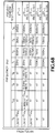
| DS | Bit Rate |
| DS0 | 64 Kbps |
| DS1 | 1.544 Mbps |
| DS1C | 3.152 Mbps |
| DS2 | 6.312 Mbps |
| DS3 | 44.736 Mbps |
| DS4E | 139.264 Mbps |
| DS4 | 274.176 Mbps |
| 64 Kbps |
| 2.048 Mbps |
| 8.448 Mbps |
| 34.368 Mbps |
| 139.263 Mbps |
| SDH/SONET Signal Hierarchy | |||
| Data Rate (Mbps) | CCITT Designation | Electrical Signal | Optical Signal |
| 51.84 | STM-0 | STS-1 | OC-1 |
| 155.52 | STM-1 | STS-3 | OC-3 |
| 622.08 | STM-4 | STS-12 | OC-12 |
| 2488.32 | STM-16 | STS-48 | OC-48 |
Claims (12)
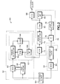
- An signal generator (50) for generating a variable phase/frequency output comprising:a variable reference oscillator (52) for generating a reference having a varying phase offset over a first phase modulation frequency interval and a constant output over a second phase modulation frequency interval;a variable oscillator (54) for generating a constant output over the first phase modulation frequency interval and a variable output over the second phase modulation frequency interval; anda phase locked loop (56) having a phase detector (74), a phase summing node (76) and oscillator (80) with the phase detector (74) coupled to receive the outputs of the variable reference oscillator (52) and the oscillator (80), and phase summing node coupled to receive the outputs of the variable oscillator (54) and the phase detector (74) wherein the output of the phase locked loop (56) tracks the variable reference oscillator (52) over the first phase modulation frequency interval and generates a phase modulated output in response to the variable output of the variable oscillator (54) over the second phase modulation frequency interval.
- The signal generator of claim 1 wherein the variable reference oscillator (52) comprises:a phase locked loop (62) for generating the reference; anda direct digital synthesizer (60) coupled to the phase locked loop (62) for generating an output for varying the phase offset of the reference over the first phase modulation frequency interval.
- The signal generator of claim 2 wherein the output of the direct digital synthesizer (60) phase modulates the variable reference oscillator (52) over the first phase modulation frequency interval.
- The signal generator of claim 2 wherein the output of the direct digital synthesizer (60) offsets the frequency of the variable reference oscillator (52).
- The signal generator of claim 2 wherein the output of the direct digital synthesizer (60) phase modulates the variable reference oscillator (52) over the first phase modulation frequency interval and offsets the frequency of the variable reference oscillator (52).
- The signal generator of claim 2 wherein the direct digital synthesizer (60) further comprises a look-up table for generating a sinusoidal output for varying the phase offset of the reference over the first phase modulation frequency interval.
- The signal generator of claim 2 wherein the variable reference oscillator further comprises a digital signal processor (58) coupled to the direct digital synthesizer (60) for generating frequency updates to the direct digital synthesizer (60) for generating the output for varying the phase offset of the reference over the first phase modulation frequency interval.
- The signal generator of claim 7 wherein the digital signal processor (58) has a sample rate for generating the frequency updates to the direct digital synthesizer (60) wherein the output of the direct digital synthesizer (60) is a function of the frequency updates producing the varying phase offset in the reference.
- The signal generator of claim 7 wherein the output of the direct digital synthesizer (60) is phase modulated by an arbitrary waveform output over the first phase modulation frequency interval.
- The signal generator as recited in claim 2 wherein the phase locked loop further comprises variable dividers (72, 82) respectively coupled between the variable reference oscillator (52) and the phase detector (74) and between the phase locked loop oscillator (80) and the phase detector (74) with the phase locked loop oscillator (80) being a voltage controlled oscillator having an octave bandwidth.
- The signal generator as recited in claim 10 further comprising a variable divider (88) coupled to the output of the phase locked loop (56) that in combination with the variable reference oscillator (52) having a direct digital synthesizer (60) and the phase locked loop (62) generates any frequency within the limits of the signal generator (50) having parts per billion resolution.
- The signal generator as recited in claim 10 further comprising a variable divider (72) coupled to the output of the variable reference oscillator (52) that in combination with the variable reference oscillator having the direct digital synthesizer (60) and the phase locked loop (62) generates any frequency within the limits of the signal generator (50) having parts per billion resolution.
Applications Claiming Priority (2)
| Application Number | Priority Date | Filing Date | Title |
|---|---|---|---|
| US08/709,024 US5742208A (en) | 1996-09-06 | 1996-09-06 | Signal generator for generating a jitter/wander output |
| US709024 | 1996-09-06 |
Publications (2)
| Publication Number | Publication Date |
|---|---|
| EP0828343A1 true EP0828343A1 (en) | 1998-03-11 |
| EP0828343B1 EP0828343B1 (en) | 2001-12-12 |
Family
ID=24848172
Family Applications (1)
| Application Number | Title | Priority Date | Filing Date |
|---|---|---|---|
| EP97306915A Expired - Lifetime EP0828343B1 (en) | 1996-09-06 | 1997-09-05 | Signal generator for generating a jitter/wander output |
Country Status (4)
| Country | Link |
|---|---|
| US (1) | US5742208A (en) |
| EP (1) | EP0828343B1 (en) |
| DE (1) | DE69709000T2 (en) |
| ES (1) | ES2170337T3 (en) |
Cited By (5)
| Publication number | Priority date | Publication date | Assignee | Title |
|---|---|---|---|---|
| DE10020686A1 (en) * | 2000-04-27 | 2001-10-31 | Siemens Ag | Circuit arrangement for generating wander or hiking sequences |
| EP1164696A1 (en) * | 1999-12-24 | 2001-12-19 | Anritsu Corporation | Wonder generator, digital line tester comprising the same, and phase noise transfer characteristic analyzer |
| EP1411661A1 (en) * | 2002-10-18 | 2004-04-21 | Agilent Technologies, Inc. - a Delaware corporation - | Apparatus and method for generating wander noise |
| EP1814218A1 (en) | 2006-01-05 | 2007-08-01 | Yokogawa Electric Corporation | Frequency synthesizer |
| US20190131981A1 (en) * | 2017-10-31 | 2019-05-02 | Nxp B.V. | Apparatus comprising a phase-locked loop |
Families Citing this family (36)
| Publication number | Priority date | Publication date | Assignee | Title |
|---|---|---|---|---|
| US6249155B1 (en) * | 1997-01-21 | 2001-06-19 | The Connor Winfield Corporation | Frequency correction circuit for a periodic source such as a crystal oscillator |
| US6016331A (en) * | 1997-08-05 | 2000-01-18 | Vlsi Technology, Inc. | Methods of synchronization, personal handy-phone system stations and phase lock loops |
| US6104222A (en) * | 1997-12-17 | 2000-08-15 | Sony Corporation | Flexible phase locked loop system |
| US6088414A (en) * | 1997-12-18 | 2000-07-11 | Alcatel Usa Sourcing, L.P. | Method of frequency and phase locking in a plurality of temporal frames |
| JP2944607B2 (en) * | 1998-02-12 | 1999-09-06 | 日本電気アイシーマイコンシステム株式会社 | Digital PLL circuit and clock generation method |
| GB9809450D0 (en) * | 1998-05-01 | 1998-07-01 | Wandel & Goltermann Limited | Jitter measurement |
| KR100328757B1 (en) * | 1999-09-07 | 2002-03-14 | 서평원 | A error preventing device of clock signal with switchover for transmission system |
| US7245685B2 (en) * | 2000-12-05 | 2007-07-17 | Ericsson Ab | Filtering for timing distribution system in networking products |
| US6614216B2 (en) * | 2001-02-07 | 2003-09-02 | Square D Company | System and method for intersample timing error reduction |
| US6654899B2 (en) * | 2001-03-28 | 2003-11-25 | Intel Corporation | Tracking bin split technique |
| JP3567905B2 (en) * | 2001-04-06 | 2004-09-22 | セイコーエプソン株式会社 | Oscillator with noise reduction function, writing device, and method of controlling writing device |
| EP1440539A4 (en) * | 2001-09-27 | 2009-08-26 | Broadcom Corp | Highly integrated media access control |
| US20030112043A1 (en) * | 2001-12-19 | 2003-06-19 | Ando Electric Co., Ltd. | PLL circuit and control method for PLL circuit |
| US7421043B2 (en) * | 2002-11-27 | 2008-09-02 | Lsi Corporation | Method and/or apparatus for stabilizing the frequency of digitally synthesized waveforms |
| US20040230997A1 (en) * | 2003-05-13 | 2004-11-18 | Broadcom Corporation | Single-chip cable set-top box |
| DE10345497B4 (en) * | 2003-09-30 | 2006-12-21 | Infineon Technologies Ag | Oscillator circuit, in particular for mobile communications |
| GB2409383B (en) * | 2003-12-17 | 2006-06-21 | Wolfson Ltd | Clock synchroniser |
| GB0412451D0 (en) * | 2004-06-04 | 2004-07-07 | Koninkl Philips Electronics Nv | Measuring clock jitter |
| US8239914B2 (en) * | 2004-07-22 | 2012-08-07 | Broadcom Corporation | Highly integrated single chip set-top box |
| RU2005102419A (en) * | 2005-02-01 | 2006-07-10 | Самсунг Электроникс Ко., Лтд. (KR) | DEVICE AND METHOD FOR NOISE SIGNAL GENERATION |
| DE102005049578A1 (en) * | 2005-10-17 | 2007-04-19 | Rohde & Schwarz Gmbh & Co. Kg | Signal generator with direct-feed DDS signal source |
| US7675369B2 (en) * | 2006-06-12 | 2010-03-09 | Honeywell International Inc. | Frequency hopping oscillator circuit |
| US20070294738A1 (en) * | 2006-06-16 | 2007-12-20 | Broadcom Corporation | Single chip cable set-top box supporting DOCSIS set-top Gateway (DSG) protocol and high definition advanced video codec (HD AVC) decode |
| US8284822B2 (en) * | 2007-02-27 | 2012-10-09 | Broadcom Corporation | Method and system for utilizing direct digital frequency synthesis to process signals in multi-band applications |
| US20080205545A1 (en) * | 2007-02-28 | 2008-08-28 | Ahmadreza Rofougaran | Method and System for Using a Phase Locked Loop for Upconversion in a Wideband Crystalless Polar Transmitter |
| US7826550B2 (en) * | 2007-02-28 | 2010-11-02 | Broadcom Corp. | Method and system for a high-precision frequency generator using a direct digital frequency synthesizer for transmitters and receivers |
| US8116387B2 (en) * | 2007-03-01 | 2012-02-14 | Broadcom Corporation | Method and system for a digital polar transmitter |
| JP5359314B2 (en) * | 2009-01-27 | 2013-12-04 | 富士通株式会社 | Transmission equipment |
| JP4933635B2 (en) * | 2010-02-19 | 2012-05-16 | 日本電波工業株式会社 | PLL circuit |
| WO2012142760A1 (en) * | 2011-04-21 | 2012-10-26 | Huawei Technologies Co., Ltd. | Phase error compensation arrangement and phase error compensation method |
| JP2013061278A (en) * | 2011-09-14 | 2013-04-04 | Fujitsu Ltd | Signal generation device and signal generation method |
| US8698567B2 (en) * | 2012-04-02 | 2014-04-15 | Avago Technologies General Ip (Singapore) Pte. Ltd. | Phase-locked loop calibration system and method |
| JP6024438B2 (en) * | 2012-12-13 | 2016-11-16 | 船井電機株式会社 | Receiver |
| RU2580068C1 (en) * | 2015-02-24 | 2016-04-10 | Акционерное общество "Научно-производственное предприятие "Исток" имени А.И. Шокина" (АО "НПП "Исток" им. Шокина") | Microwave frequency synthesizer |
| TWI663837B (en) * | 2018-03-13 | 2019-06-21 | 群聯電子股份有限公司 | Phase-locked loop circuit calibration method, memory storage device and connection interface circuit |
| CN114201435B (en) * | 2021-12-01 | 2024-03-05 | 北京奕斯伟计算技术股份有限公司 | Clock generator, detection system and signal output method |
Citations (5)
| Publication number | Priority date | Publication date | Assignee | Title |
|---|---|---|---|---|
| US4516084A (en) * | 1983-02-18 | 1985-05-07 | Rca Corporation | Frequency synthesizer using an arithmetic frequency synthesizer and plural phase locked loops |
| US4810977A (en) * | 1987-12-22 | 1989-03-07 | Hewlett-Packard Company | Frequency modulation in phase-locked loops |
| GB2247368A (en) * | 1990-08-25 | 1992-02-26 | Roke Manor Research | Phase modulation signal generator |
| EP0547271A1 (en) * | 1991-12-18 | 1993-06-23 | Hewlett-Packard Limited | Method and apparatus for generating test signals |
| US5515404A (en) * | 1993-06-24 | 1996-05-07 | Madge Networks Limited | Data communication systems |
Family Cites Families (4)
| Publication number | Priority date | Publication date | Assignee | Title |
|---|---|---|---|---|
| FI90169C (en) * | 1991-12-31 | 1993-12-27 | Nokia Mobile Phones Ltd | FOERFARANDE OCH KOPPLINGSARRANGEMANG FOER ATT ALSTRA EN MODULERAD SIGNAL |
| JP2825045B2 (en) * | 1992-08-05 | 1998-11-18 | 日本電気株式会社 | Frequency synthesizer |
| JPH06177651A (en) * | 1992-12-08 | 1994-06-24 | Uniden Corp | Frequency synthesizer |
| US5424688A (en) * | 1993-07-02 | 1995-06-13 | Rockwell International Corp. | Frequency synthesizer apparatus incorporating phase modulation tracking means |
-
1996
- 1996-09-06 US US08/709,024 patent/US5742208A/en not_active Expired - Fee Related
-
1997
- 1997-09-05 ES ES97306915T patent/ES2170337T3/en not_active Expired - Lifetime
- 1997-09-05 DE DE69709000T patent/DE69709000T2/en not_active Expired - Fee Related
- 1997-09-05 EP EP97306915A patent/EP0828343B1/en not_active Expired - Lifetime
Patent Citations (5)
| Publication number | Priority date | Publication date | Assignee | Title |
|---|---|---|---|---|
| US4516084A (en) * | 1983-02-18 | 1985-05-07 | Rca Corporation | Frequency synthesizer using an arithmetic frequency synthesizer and plural phase locked loops |
| US4810977A (en) * | 1987-12-22 | 1989-03-07 | Hewlett-Packard Company | Frequency modulation in phase-locked loops |
| GB2247368A (en) * | 1990-08-25 | 1992-02-26 | Roke Manor Research | Phase modulation signal generator |
| EP0547271A1 (en) * | 1991-12-18 | 1993-06-23 | Hewlett-Packard Limited | Method and apparatus for generating test signals |
| US5515404A (en) * | 1993-06-24 | 1996-05-07 | Madge Networks Limited | Data communication systems |
Cited By (12)
| Publication number | Priority date | Publication date | Assignee | Title |
|---|---|---|---|---|
| EP1164696A1 (en) * | 1999-12-24 | 2001-12-19 | Anritsu Corporation | Wonder generator, digital line tester comprising the same, and phase noise transfer characteristic analyzer |
| EP1164696A4 (en) * | 1999-12-24 | 2003-07-23 | Anritsu Corp | Wander generator, digital line tester comprising the same, and phase noise transfer characteristic analyzer |
| US7206339B2 (en) | 1999-12-24 | 2007-04-17 | Anritsu Corporation | Wonder generator, digital line tester comprising the same, and phase noise transfer characteristic analyzer |
| US7450633B2 (en) | 1999-12-24 | 2008-11-11 | Anritsu Corporation | Wander generator, and digital line tester and phase noise transfer characteristic analyzer using the same |
| DE10020686A1 (en) * | 2000-04-27 | 2001-10-31 | Siemens Ag | Circuit arrangement for generating wander or hiking sequences |
| DE10020686C2 (en) * | 2000-04-27 | 2002-05-02 | Siemens Ag | Circuit arrangement for generating wander or hiking sequences |
| US6847264B2 (en) | 2000-04-27 | 2005-01-25 | Siemens Aktiengesellschaft | Method for generating wander or wander sequences |
| EP1411661A1 (en) * | 2002-10-18 | 2004-04-21 | Agilent Technologies, Inc. - a Delaware corporation - | Apparatus and method for generating wander noise |
| US7020568B2 (en) | 2002-10-18 | 2006-03-28 | Agilent Technologies, Inc. | Apparatus and method for generating wander noise |
| EP1814218A1 (en) | 2006-01-05 | 2007-08-01 | Yokogawa Electric Corporation | Frequency synthesizer |
| US20190131981A1 (en) * | 2017-10-31 | 2019-05-02 | Nxp B.V. | Apparatus comprising a phase-locked loop |
| US10594327B2 (en) * | 2017-10-31 | 2020-03-17 | Nxp B.V. | Apparatus comprising a phase-locked loop |
Also Published As
| Publication number | Publication date |
|---|---|
| ES2170337T3 (en) | 2002-08-01 |
| DE69709000D1 (en) | 2002-01-24 |
| DE69709000T2 (en) | 2002-08-29 |
| EP0828343B1 (en) | 2001-12-12 |
| US5742208A (en) | 1998-04-21 |
Similar Documents
| Publication | Publication Date | Title |
|---|---|---|
| EP0828343B1 (en) | Signal generator for generating a jitter/wander output | |
| US5754437A (en) | Phase measurement apparatus and method | |
| US5757652A (en) | Electrical signal jitter and wander measurement system and method | |
| JP3092352B2 (en) | Apparatus and method for desynchronized SONET with DS-N signal | |
| US6415006B2 (en) | Reducing waiting time jitter | |
| EP0626117B1 (en) | Desynchronizer and method for suppressing pointer jitter in a desynchronizer | |
| Bellamy | Digital network synchronization | |
| USRE45557E1 (en) | Configurable voltage controlled oscillator system and method including dividing forming a portion of two or more divider paths | |
| US20070019772A1 (en) | Timeshared jitter attenuator in multi-channel mapping applications | |
| EP1436923B1 (en) | Method and apparatus for digital data synchronization | |
| US5777998A (en) | Method and circuit arrangement for the realization of the higher path adaptation/mapping function in synchronous digital hierarchy/optical network equipment | |
| US5430659A (en) | Method and apparatus for generating signals | |
| US6658074B1 (en) | Method and apparatus for reproducing clock signal of low order group signal | |
| EP0707393B1 (en) | Fractional bit-leaking clock signal resynchronizer for a highspeed digital communications system | |
| US7440533B2 (en) | Modulated jitter attenuation filter | |
| Sari et al. | Cancelation of pointer adjustment jitter in SDH networks | |
| Bregni et al. | Jitter testing technique and results at VC-4 desynchronizer output of SDH equipment | |
| WO1993016535A1 (en) | Pointer jitter suppression in a desynchronizer | |
| US6587533B1 (en) | Method for attenuating transients caused by aligning in a desynchronizer | |
| Sholander et al. | Effects of fixed frequency clock offsets in synchronous digital hierarchy networks | |
| Klein et al. | SONET/SDH pointer processor implementations | |
| Sholander et al. | Mapping wander in SONET/SDH fixed threshold and uniform pointer processors | |
| KR20040057018A (en) | Synchronization system for synchronous multiplexer | |
| KR20030014077A (en) | Pointer adjustment synchronization system using threshold modulation technique | |
| KR100338696B1 (en) | synchronization system |
Legal Events
| Date | Code | Title | Description |
|---|---|---|---|
| PUAI | Public reference made under article 153(3) epc to a published international application that has entered the european phase |
Free format text: ORIGINAL CODE: 0009012 |
|
| AK | Designated contracting states |
Kind code of ref document: A1 Designated state(s): AT BE CH LI |
|
| AX | Request for extension of the european patent |
Free format text: AL;LT;LV;RO;SI |
|
| 17P | Request for examination filed |
Effective date: 19980806 |
|
| AKX | Designation fees paid |
Free format text: AT BE CH LI |
|
| RBV | Designated contracting states (corrected) |
Designated state(s): AT BE CH LI |
|
| REG | Reference to a national code |
Ref country code: DE Ref legal event code: 8566 |
|
| 17Q | First examination report despatched |
Effective date: 20000524 |
|
| GRAG | Despatch of communication of intention to grant |
Free format text: ORIGINAL CODE: EPIDOS AGRA |
|
| GRAG | Despatch of communication of intention to grant |
Free format text: ORIGINAL CODE: EPIDOS AGRA |
|
| GRAH | Despatch of communication of intention to grant a patent |
Free format text: ORIGINAL CODE: EPIDOS IGRA |
|
| GRAH | Despatch of communication of intention to grant a patent |
Free format text: ORIGINAL CODE: EPIDOS IGRA |
|
| GRAA | (expected) grant |
Free format text: ORIGINAL CODE: 0009210 |
|
| AK | Designated contracting states |
Kind code of ref document: B1 Designated state(s): DE ES GB |
|
| REG | Reference to a national code |
Ref country code: GB Ref legal event code: IF02 |
|
| REF | Corresponds to: |
Ref document number: 69709000 Country of ref document: DE Date of ref document: 20020124 |
|
| RAP2 | Party data changed (patent owner data changed or rights of a patent transferred) |
Owner name: TEKTRONIX, INC. |
|
| REG | Reference to a national code |
Ref country code: ES Ref legal event code: FG2A Ref document number: 2170337 Country of ref document: ES Kind code of ref document: T3 |
|
| PLBE | No opposition filed within time limit |
Free format text: ORIGINAL CODE: 0009261 |
|
| STAA | Information on the status of an ep patent application or granted ep patent |
Free format text: STATUS: NO OPPOSITION FILED WITHIN TIME LIMIT |
|
| 26N | No opposition filed | ||
| PGFP | Annual fee paid to national office [announced via postgrant information from national office to epo] |
Ref country code: GB Payment date: 20040817 Year of fee payment: 8 |
|
| PGFP | Annual fee paid to national office [announced via postgrant information from national office to epo] |
Ref country code: DE Payment date: 20040818 Year of fee payment: 8 |
|
| PGFP | Annual fee paid to national office [announced via postgrant information from national office to epo] |
Ref country code: ES Payment date: 20040906 Year of fee payment: 8 |
|
| PG25 | Lapsed in a contracting state [announced via postgrant information from national office to epo] |
Ref country code: GB Free format text: LAPSE BECAUSE OF NON-PAYMENT OF DUE FEES Effective date: 20050905 |
|
| PG25 | Lapsed in a contracting state [announced via postgrant information from national office to epo] |
Ref country code: ES Free format text: LAPSE BECAUSE OF NON-PAYMENT OF DUE FEES Effective date: 20050906 |
|
| PG25 | Lapsed in a contracting state [announced via postgrant information from national office to epo] |
Ref country code: DE Free format text: LAPSE BECAUSE OF NON-PAYMENT OF DUE FEES Effective date: 20060401 |
|
| GBPC | Gb: european patent ceased through non-payment of renewal fee |
Effective date: 20050905 |
|
| REG | Reference to a national code |
Ref country code: ES Ref legal event code: FD2A Effective date: 20050906 |