The present invention relates to an innovative operation and architecture for a
DRAM system (a memory array system constituted by DRAMS). More
specifically, the present invention relates to an innovative operation and architecture
for a DRAM system that fully utilises the high-bandwidth capability and
enables high speed processing.
With DRAMs, an inexpensive memory system having a large memory capacity
can be constructed by using an extremely simple structure. DRAMS are,
therefore, the optimal selection for a memory device to be used in a computer
system. The transfer speed of DRAMS (called the bandwidth, generally
represented as a product of a data width and a clock rate) is slower than that of
SRAMS, another memory device. The bandwidth of DRAMS cannot keep up
with the recent enhancement of the speed of MPUs, and becomes one of the
barriers to improving the performance of a computer system. Conventionally,
various ideas have been provided to improve the bandwidth of DRAMS.
Examples are synchronous DRAMS (SDRAM) and rambus DRAMS (RDRAM),
which adopt a system for reading/writing consecutive address data in
synchronisation with a high speed clock. In a system that uses a high speed
clock, theoretically, its input/output section can be operated at 100 to 250 MHz
(SDRAM) or at 500 to 600 MHz (RDRAM), which is the operational speed of the
clock. However, an activation and precharge operation for a memory array is
required for a memory array that is connected to the input/output section. As a
result, the bandwidth of the entire memory system, including the input/output
section and the memory array, is drastically reduced. For example, when a clock
of 200 MHz is employed for SDRAM and when data width is 16 bits (two bytes),
a specific value for the bandwidth can be 400 MB/s (400 MB per second).
However, if the activation and precharge operation for the memory array is
included, the bandwidth is reduced to about one third, 146 MB/s. This is due to
the fact that two array activation and precharge operations are required to
read/write 4-bit consecutive data, and a period equivalent to 22 clock cycles is
spent for these operations. The same thing can be applied for RDRAM. A high
speed clock cycle of 500 MHz can not be employed effectively, and the actual
operating speed is reduced to 25% to 40%. For RDRAM, if a hit miss occurs, an
extremely long time (e.g., 140 ns) is required, and the bandwidth is drastically
reduced.
As is described above, the main factor related to the reduction of the bandwidth in
a system is the time required for the activation and precharge operation of the
memory array. In the above system, therefore, multiple banks (memory array
blocks) are prepared and the activation and precharge operation is performed for
each bank, independently. The activation and precharge operation for one bank is
being performed while another bank is being accessed, so that the period required
for the activation and precharge operation is hidden and the bandwidth is
improved. A specific example of such a system is the SyncLink system (NIKKEI
MICRODEVICES, August 1995, p.152). This system independently performs
data reading and writing for a memory array that is divided into multiple banks.
With this system, however, while a seamless operation is ensured when different
banks are sequentially accessed, a seamless operation cannot be provided when
the same bank is accessed continuously. This being taken into account, the
average data rate is considerably reduced.
To increase processing speed using the conventional methods, it is always
premised that different banks will be sequentially accessed. This is because when
a specific bank is accessed and continues to be accessed thereafter, the
performance of the activation and precharge operation for memory cells in that
bank is still required and this processing cannot be hidden. It is well known that
data accesses are not always performed alternately for the other banks. Therefore,
the above described method, which can be called an alternate bank access system,
does not provide an effective resolution for the problem. In addition, the provision
of multiple banks adversely affect the installation and product inspection
costs, which are not acceptable.
To overcome the shortcoming of the method whereby multiple banks are
provided, the present inventors disclosed, in "A Full bit Prefetch Architecture For
Synchronous DRAMs" (IEEE JSSC, Vol. SC-30, No. 9, September 1995, pp.
998-1005) and in Japanese Unexamined Patent Publication No. Hei 07-283849),
a system whereby a local latch that is provided for each set of 32 bit lines, of 256
bit lines connected to a memory array, latches a total of eight data bits, and
whereby the eight local latches are connected to a local buffer to perform a burst
series transfer of data. This reading mechanism is called a prefetch system,
because the data are fetched in advance to the local latches. For data reading
from SDRAM this system can satisfactorily compensate for a reduction in the
bandwidth, and can provide a seamless operation (provides a condition where
there are no unnecessary clock cycles between data transfers). However, with
this system a seamless operation is not possible during data writing.
The present inventors disclosed, in "A Full Bit Prefetch DRAMS Sensing
Circuit" (IEEE JSSC, Vol. SC-31, No. 6, September 1996, pp. 762-772), a
configuration whereby a full burst of read data is latched by an I/O sense
amplifier by a single CAS access. With this configuration, the precharging can
start two clocks before the data burst cycle begins. Since the precharging can be
performed early, during the burst reading of preceding data, the subsequent RAS
and CAS accesses can be performed. When eight bits are employed as a burst
length, seamless reading can be performed even though the same bank is
accessed. With this method, however, the seamless writing cannot be ensured.
It is therefore a first object of the present invention to provide a DRAMS system
that, with respect to clock pulse frequency, prevents substantial reduction of
bandwidth. That is, the object is to provide a memory system that has a
bandwidth the equivalent of that for an input/output circuit.
It is a second object of the present invention to provide a memory system
constituted by DRAMS, with which the first object is achieved, even when banks
are accessed in no specific order.
It is a third object of the present invention to provide a memory system
constituted by DRAMS whereby a seamless operation is assured not only for
reading but also for writing.
It is a fourth object of the present invention to provide a function that can
seamlessly perform simultaneous read and write operations.
It is a fifth object of the present invention to provide a DRAMS memory system
that achieves the first through the fourth object by employing an improved
prefetch system.
To achieve the above objects, according to the present invention, a prefetch
mechanism is applied for writing data to separate memory array at an early stage,
so that the activation and precharge operation, which must be done before reading
the next set of data from the memory array, does not affect nor cause any
deterioration of access speed. An amount of data is prefetched that is twice as
much as that fetched in the period represented by an array time constant, so that
in a single bank structure a seamless operation can be achieved both for reading
and for writing, even when accesses to any row addresses are involved.
More specifically, according to the present invention, a memory system
comprises: a memory array consisting of multiple memory devices, an input data
path for inputting external data, an output data path for externally outputting data,
an input data bit storage mechanism located between the memory array and the
input data path, and an output data bit storage mechanism located between the
memory array and the output data path and is characterised in that data bits read
from the memory array are held in the output data bit storage mechanism for
external output across the output data path and an activation and prefetch
operation is effected, which is required for a following data reading from the
memory array. In addition, according to the present invention, by using such a
memory system, data bits are transferred in advance from a memory array to an
output data bit storage mechanism and a first burst output is performed. During
this period, an operation required for a following data reading from the memory
array is executed, and a next read address is assured. Then, more data bits are
transferred from the memory array to the output data bit storage mechanism to
perform a second burst output seamlessly, relative to the first burst output. In a
write mode, external data bits are stored in input data bit storage means. The
procedure at this step can be performed without being affected by the timings for
the first and the second burst outputs. This is because the input data bit storage
means and the output data bit storage means can be operated independently.
How the invention may be carried out will now be classified by way of example
only and with reference to the accompanying drawings in which :
The condition for implementing a seamless operation is the condition that exists
when a sum of a RAS-CAS delay (tRCD) and a RAS precharge time (tRP) is smaller
than a burst length (LB), i.e.,
tRCD + tRP < LB
These times are actually represented by a number of clock cycles. Even when
data accesses are performed between any row addresses at this time, a seamless
operation can be assured. That is, even when an activation and precharge
operation for a memory array is included, continuous reading/writing can be performed.
Since tRCD + tRP on the left side of the above expression represents the minimum
period of time required for accessing the memory array, this value is called an
array time constant. Assuming that reading and writing are alternately performed
during regular processing, the actual condition for the seamless operation can be
defined as:
2(tRCD + tRP) < LB
To provide the above condition, according to the present invention, in the
memory system constituted by a DRAM, the memory array and the data
input/output circuits are connected together by a latch, etc., and their operations
can be separated. Further, the input circuit and the output circuit are provided
separately to ensure independent operations, and reduction of the bandwidth does
not occur while reading and writing are repeated alternately.
Fig. 1 is a specific diagram illustrating one embodiment of the present invention.
Memory arrays 1 and 2 are connected to an input circuit 20 and an output circuit
30 via a read/write latch 10. The input circuit 20 and the output circuit 30 are
connected to external devices via a receiver and an input pin 21, and via an output
buffer and an output pin 31 respectively. Four input latches 26, 27, 28 and 29 are
provided for data input and four output latches 46, 47, 48 and 49 are provided for
data output. These input latches are constituted by multiple input data paths 22,
23, 24 and 25, and the output latches are constituted by multiple output data paths
32, 33, 34 and 35.
Fig. 2 is a detailed diagram illustrating the circuit shown in Fig. 1. The read/write
latch 10 is actually separated into read latches 12 and write latches 11. Each set
of four latches is connected to one of the data paths 22 to 25, and the data paths
32 to 35. In this embodiment, since four data paths are employed for reading and
four for writing, and since four latches are connected to each data path, sixteen
write latches and sixteen read latches are distributed among 256 bit lines. In
other words, one latch is provided for every 16 bit lines.
The number of latches to be allocated for each bit line set of the 256 bit lines is
determined by the time array constant and the clock frequency. For a common 16
to 64 MB DRAMS, the array time constant is 32 ns. When the data clock
frequency is 250 MHz (4ns), from the above expression (2) it is apparent that
only a 16-bit burst transfer need be performed. To do this, 16 latches must be
provided for each bit line set of the 256 bit lines, and must prefetch to prepare for
a 16-bit burst transfer. As is described above, the arrangement in Fig. 2 is only an
example acquired by employing a specific array time constant and a specific
clock frequency. The present invention is not limited to the arrangement in Fig.
2.
In this invention, an activation and precharge operation for a memory array is
performed while data are being latched. This is the same as the above described
background art. In the configuration in Fig. 2, 16 bits are latched during an array
time constant period of 32 ns. Every 16 ns the latches output one bit set having a
4-bit width to each of the four output data paths via read buffers 36, 37, 38 and
39, which are connected to the respective output data paths 32 to 35. And every 4
ns (250 MHz) the data are output to the exterior across the output data paths by
using the output latches and the output buffers. In this manner, the 16-bit burst
output can be completed within a total of 64 ns, and expression (2) can be
satisfied.
For a write mode, the 4-bit latches 26, 27, 28 and 29 shown in Fig. 1 are provided
for input. The 4-bit latches drive the input data paths every 16 ns to store bit sets
having a 4-bit width in the write latch 11. When all 16 bits have been stored, data
writing to the memory array is performed.
The processing for the circuit in Fig. 2 will now be described in detail. In a read
mode, a switch RG(U) 61 or a switch RG(L) 62 goes high. When the switch
RG(U) 61 goes high, the memory array 1 is selected. When the switch RG(L) 62
goes high, the memory array 2 is selected. Fig. 3 is a timing chart in a read mode
when the switch RG(U) 61 goes high. Since the switch RG(U) 61 goes high, the
TRUE (T)/COMPLEMENT (C) line of a sense amplifier connected to the
memory array 1 is connected to the read latch 42 across the switch RG(U) 61.
Since the switch RG(L) 62 does not go high, the memory array 2 is not connected
to the read latch 42. In this condition, 1-bit data from the sense amplifier is
latched in advance by the read latch 42. A read latch 42 is provided for every 16
bits of the sense amplifier, and a total of sixteen bits are provided for a memory
array (256 bit width). As is described above, one of the read buffers 36, 37, 38
and 39 for external output are provided for every 64 bits, and is connected to the
read latches via switch RG1, RG2, RG3 and RG4 (not shown except for the latch
42). Hereinafter, a sense amplifier unit of 64-bit lines is called a block for
convenience sake.
By employing the block concept, the present invention is configured as follows.
The sense amplifier having a 256 bit width is constituted by four blocks having
64 bit widths. The buffers 36, 37, 38 and 39 are respectively connected to the
four blocks for outputting. These buffers can increase the driving force for the
output, but for them to perform the latch bit function is not inevitable. Each
block has four read latches 42. The four read latches 42 are connected to one data
path (e.g., the data path 32) across a connected buffer to each block and to the
switches RG1, RG2, RG3 and RG4. The switches RG1, RG2, RG3 and RG4 go
high sequentially at intervals one quarter the length of the cycle time required for
the switch RG(U) to go high, as is shown by the timing chart in Fig. 3. When the
switch RG1 goes high, for example, bits stored in the read latch 42 (D1) are
output externally from the buffer 36. Then, the switch RG 2 goes high, and bits
stored in the connecting read latch 42 (D2) are output externally from the buffer
36. This process is repeated for the switches RG3 and RG4, and data D3 and D4
are output externally via the buffer 36. This operation is performed for each
block. Since there are four blocks in the memory array (256 bit width) and four
corresponding buffers and data paths are arranged, data are output externally as
units of four bits, as is shown in Fig. 3. More specifically, in respective blocks,
corresponding data to the condition where the switch RG 1 goes high are output
in parallel through the respective buffers 36, 37, 38 and 39 by the output latches
46, 47, 48 and 49 that are connected to the buffers. As is shown in Fig. 1, since
the data from the output latches 46, 47, 48 and 49 are finally output externally
through one output pin 31, four sets of parallel data are output externally in a
burst mode while timings are gradually delayed by using a clock four times as
fast.
The write mode will now be described. In the write mode, data are input in
advance to the input latches 26, 27, 28 and 29 at a timing four times as fast. As
switches WG1, WG2, WG3 and WG4 go high sequentially, as is shown in Fig. 4,
four bits of data are stored in the write latch 41 and in corresponding write latches
(not shown) in the other blocks. More specifically, there are four blocks in the
memory array and they are connected to the data paths 22, 23, 24 and 25
respectively. The four switches WG1, WG2, WG3 and WG4 are connected to
each data path. Therefore, when the switch WG1 goes high relative to the data
paths 22, 23, 24 and 25, as is shown in Fig. 4, 4 bits of data (D1) are stored in
each of the four write latches. This process is repeated as the switches WG2,
WG3 and WG4 go high in order, and a total of 16 bits data are stored, one to each
of the 16 write latches. When the switch WG(U) goes high after this processing
sequence has been completed, 16 bits of data are stored in the memory array in a
burst mode. As is shown in Fig. 4, since all of the data bits are stored in the write
latches at the same time as the switch WG4 goes high, the switch WG(U) can go
high at the same time the switch WG4 goes high.
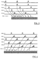
Fig. 6 is a timing chart for explaining the operation of a DRAMS system
according to the present invention, compared with a conventional SDRAM
system (Fig. 5). The burst length for the conventional SDRAM system is four
and the burst length for the DRAMS system of the present invention is sixteen, at
a clock frequency for both of them is 125 MHz.
Referring to Fig. 5, in the SDRAM, row address R1 and column address C1 are
determined by the leading edges (activation) of RAS and CAS. Based on these
addresses, four data bits are output continuously in a burst mode. But when a
4-bit burst has been completed, as the activation and precharge operation for a
memory array takes much time, the designation of the next row address R2 and
column address C2 is delayed. Therefore, a succeeding 4-bit burst cannot be
performed following a preceding 4-bit burst. That is, when the same bank is
accessed, a seamless operation cannot be performed.
Referring to Fig. 6, for the conventional SDRAM, the row address and the
column address are designated by the leading edges of the RAS and CAS. Data
reading begin in a 16-bit burst mode based on the first address (R1, C1). As is
described above, the 16-bit burst is performed by a read latch group that operates
separately from the memory array. During the 16-bit burst transfer, operations
required for the next burst transfer, such as an activation and precharge operation
for a memory array, can be performed. These memory operations are completed
when the address (R3, C3) for a following data reading is designated, because the
period required for the 16-bit burst satisfies the above expression (1).
When the access is only for reading, a seamless operation can be assured with a
shorter burst length than the timing shown in Fig. 6. However, actually the
writing operation is also performed as needed in addition to the reading. In the
present invention, expression (2) where the burst length is longer than that in
expression (1) is employed. Then, an address for writing can be specified during
the read data burst transfer, and writing can be performed at the same time as the
burst transfer for reading. Referring to Fig. 6, the reading burst transfer address is
specified by the row address R1 and the column address C1. Before the burst
transfer is completed, burst transfer addresses R3 and C3 for a following data
reading are designated, and the burst transfer addresses R2 and C2 for writing are
selected. Thus, even when the writing operation is interrupted during the burst
transfer for reading, the reading operation will not be halted. This is because the
burst length that satisfies the expression (2) is employed, and because the
mechanism for independently performing the reading and writing is employed.
The read latch 11 and the write latch 12 are designed to be operated
independently in order to separately perform the reading and writing operations.
According to the present invention, provided is a DRAMS system that can
prevent a substantial reduction in bandwidth with respect to a clock pulse
frequency even when banks are accessed in no specific order. As a result,
provided is a memory system constituted by DRAMS whereby a seamless
operation is assured not only for reading but also for writing.