EP0834243B1 - Photolithographically patterned spring contact - Google Patents
Photolithographically patterned spring contact Download PDFInfo
- Publication number
- EP0834243B1 EP0834243B1 EP96916778A EP96916778A EP0834243B1 EP 0834243 B1 EP0834243 B1 EP 0834243B1 EP 96916778 A EP96916778 A EP 96916778A EP 96916778 A EP96916778 A EP 96916778A EP 0834243 B1 EP0834243 B1 EP 0834243B1
- Authority
- EP
- European Patent Office
- Prior art keywords
- contact
- substrate
- spring
- spring contact
- contacts
- Prior art date
- Legal status (The legal status is an assumption and is not a legal conclusion. Google has not performed a legal analysis and makes no representation as to the accuracy of the status listed.)
- Expired - Lifetime
Links
- 239000000758 substrate Substances 0.000 claims description 93
- 239000000523 sample Substances 0.000 claims description 62
- 238000012360 testing method Methods 0.000 claims description 26
- 238000000034 method Methods 0.000 claims description 25
- 239000004020 conductor Substances 0.000 claims description 11
- 239000000463 material Substances 0.000 claims description 9
- 238000000151 deposition Methods 0.000 claims description 8
- 239000013013 elastic material Substances 0.000 claims description 8
- 238000005530 etching Methods 0.000 claims description 7
- 239000011159 matrix material Substances 0.000 claims description 6
- 238000000059 patterning Methods 0.000 claims description 6
- 239000004065 semiconductor Substances 0.000 claims description 6
- 230000000007 visual effect Effects 0.000 claims description 3
- 229910001092 metal group alloy Inorganic materials 0.000 claims description 2
- 239000000126 substance Substances 0.000 claims description 2
- 229910052751 metal Inorganic materials 0.000 description 49
- 239000002184 metal Substances 0.000 description 49
- 229910000679 solder Inorganic materials 0.000 description 17
- 239000007789 gas Substances 0.000 description 12
- 239000000428 dust Substances 0.000 description 8
- PXHVJJICTQNCMI-UHFFFAOYSA-N Nickel Chemical compound [Ni] PXHVJJICTQNCMI-UHFFFAOYSA-N 0.000 description 6
- 229910001093 Zr alloy Inorganic materials 0.000 description 5
- 239000000853 adhesive Substances 0.000 description 5
- 230000001070 adhesive effect Effects 0.000 description 5
- ZSJFLDUTBDIFLJ-UHFFFAOYSA-N nickel zirconium Chemical compound [Ni].[Zr] ZSJFLDUTBDIFLJ-UHFFFAOYSA-N 0.000 description 5
- 238000012545 processing Methods 0.000 description 5
- XUIMIQQOPSSXEZ-UHFFFAOYSA-N Silicon Chemical compound [Si] XUIMIQQOPSSXEZ-UHFFFAOYSA-N 0.000 description 4
- 238000000137 annealing Methods 0.000 description 4
- 238000003491 array Methods 0.000 description 4
- 230000007423 decrease Effects 0.000 description 4
- PCHJSUWPFVWCPO-UHFFFAOYSA-N gold Chemical compound [Au] PCHJSUWPFVWCPO-UHFFFAOYSA-N 0.000 description 4
- 229910052737 gold Inorganic materials 0.000 description 4
- 239000010931 gold Substances 0.000 description 4
- 239000004973 liquid crystal related substance Substances 0.000 description 4
- 238000002844 melting Methods 0.000 description 4
- 230000008018 melting Effects 0.000 description 4
- 238000003825 pressing Methods 0.000 description 4
- 229910052710 silicon Inorganic materials 0.000 description 4
- 239000010703 silicon Substances 0.000 description 4
- 229910052782 aluminium Inorganic materials 0.000 description 3
- XAGFODPZIPBFFR-UHFFFAOYSA-N aluminium Chemical compound [Al] XAGFODPZIPBFFR-UHFFFAOYSA-N 0.000 description 3
- 238000013461 design Methods 0.000 description 3
- 238000004519 manufacturing process Methods 0.000 description 3
- 229910052759 nickel Inorganic materials 0.000 description 3
- XKRFYHLGVUSROY-UHFFFAOYSA-N Argon Chemical compound [Ar] XKRFYHLGVUSROY-UHFFFAOYSA-N 0.000 description 2
- 229910052581 Si3N4 Inorganic materials 0.000 description 2
- QCWXUUIWCKQGHC-UHFFFAOYSA-N Zirconium Chemical compound [Zr] QCWXUUIWCKQGHC-UHFFFAOYSA-N 0.000 description 2
- 238000005229 chemical vapour deposition Methods 0.000 description 2
- 238000004891 communication Methods 0.000 description 2
- 239000011810 insulating material Substances 0.000 description 2
- 229910021421 monocrystalline silicon Inorganic materials 0.000 description 2
- HQVNEWCFYHHQES-UHFFFAOYSA-N silicon nitride Chemical compound N12[Si]34N5[Si]62N3[Si]51N64 HQVNEWCFYHHQES-UHFFFAOYSA-N 0.000 description 2
- 238000004544 sputter deposition Methods 0.000 description 2
- 238000010561 standard procedure Methods 0.000 description 2
- 229910052726 zirconium Inorganic materials 0.000 description 2
- 229910001182 Mo alloy Inorganic materials 0.000 description 1
- 229910045601 alloy Inorganic materials 0.000 description 1
- 239000000956 alloy Substances 0.000 description 1
- 229910052786 argon Inorganic materials 0.000 description 1
- 239000012141 concentrate Substances 0.000 description 1
- 238000007796 conventional method Methods 0.000 description 1
- 238000001816 cooling Methods 0.000 description 1
- 230000003247 decreasing effect Effects 0.000 description 1
- 230000008021 deposition Effects 0.000 description 1
- 238000007772 electroless plating Methods 0.000 description 1
- 238000000313 electron-beam-induced deposition Methods 0.000 description 1
- 239000011521 glass Substances 0.000 description 1
- AMGQUBHHOARCQH-UHFFFAOYSA-N indium;oxotin Chemical compound [In].[Sn]=O AMGQUBHHOARCQH-UHFFFAOYSA-N 0.000 description 1
- 238000010849 ion bombardment Methods 0.000 description 1
- 150000002500 ions Chemical class 0.000 description 1
- 238000012986 modification Methods 0.000 description 1
- 230000004048 modification Effects 0.000 description 1
- TWNQGVIAIRXVLR-UHFFFAOYSA-N oxo(oxoalumanyloxy)alumane Chemical compound O=[Al]O[Al]=O TWNQGVIAIRXVLR-UHFFFAOYSA-N 0.000 description 1
- 238000004806 packaging method and process Methods 0.000 description 1
- 238000002161 passivation Methods 0.000 description 1
- 238000001020 plasma etching Methods 0.000 description 1
- 238000005201 scrubbing Methods 0.000 description 1
- 230000035939 shock Effects 0.000 description 1
- 239000002904 solvent Substances 0.000 description 1
- 238000002207 thermal evaporation Methods 0.000 description 1
- 238000001039 wet etching Methods 0.000 description 1
Images


Classifications
-
- H—ELECTRICITY
- H05—ELECTRIC TECHNIQUES NOT OTHERWISE PROVIDED FOR
- H05K—PRINTED CIRCUITS; CASINGS OR CONSTRUCTIONAL DETAILS OF ELECTRIC APPARATUS; MANUFACTURE OF ASSEMBLAGES OF ELECTRICAL COMPONENTS
- H05K1/00—Printed circuits
- H05K1/02—Details
- H05K1/14—Structural association of two or more printed circuits
-
- H—ELECTRICITY
- H01—ELECTRIC ELEMENTS
- H01L—SEMICONDUCTOR DEVICES NOT COVERED BY CLASS H10
- H01L24/00—Arrangements for connecting or disconnecting semiconductor or solid-state bodies; Methods or apparatus related thereto
- H01L24/71—Means for bonding not being attached to, or not being formed on, the surface to be connected
- H01L24/72—Detachable connecting means consisting of mechanical auxiliary parts connecting the device, e.g. pressure contacts using springs or clips
-
- G—PHYSICS
- G01—MEASURING; TESTING
- G01R—MEASURING ELECTRIC VARIABLES; MEASURING MAGNETIC VARIABLES
- G01R1/00—Details of instruments or arrangements of the types included in groups G01R5/00 - G01R13/00 and G01R31/00
- G01R1/02—General constructional details
- G01R1/06—Measuring leads; Measuring probes
- G01R1/067—Measuring probes
- G01R1/06711—Probe needles; Cantilever beams; "Bump" contacts; Replaceable probe pins
- G01R1/06716—Elastic
-
- G—PHYSICS
- G01—MEASURING; TESTING
- G01R—MEASURING ELECTRIC VARIABLES; MEASURING MAGNETIC VARIABLES
- G01R1/00—Details of instruments or arrangements of the types included in groups G01R5/00 - G01R13/00 and G01R31/00
- G01R1/02—General constructional details
- G01R1/06—Measuring leads; Measuring probes
- G01R1/067—Measuring probes
- G01R1/073—Multiple probes
- G01R1/07307—Multiple probes with individual probe elements, e.g. needles, cantilever beams or bump contacts, fixed in relation to each other, e.g. bed of nails fixture or probe card
- G01R1/07342—Multiple probes with individual probe elements, e.g. needles, cantilever beams or bump contacts, fixed in relation to each other, e.g. bed of nails fixture or probe card the body of the probe being at an angle other than perpendicular to test object, e.g. probe card
-
- G—PHYSICS
- G01—MEASURING; TESTING
- G01R—MEASURING ELECTRIC VARIABLES; MEASURING MAGNETIC VARIABLES
- G01R1/00—Details of instruments or arrangements of the types included in groups G01R5/00 - G01R13/00 and G01R31/00
- G01R1/02—General constructional details
- G01R1/06—Measuring leads; Measuring probes
- G01R1/067—Measuring probes
- G01R1/073—Multiple probes
- G01R1/07307—Multiple probes with individual probe elements, e.g. needles, cantilever beams or bump contacts, fixed in relation to each other, e.g. bed of nails fixture or probe card
- G01R1/07357—Multiple probes with individual probe elements, e.g. needles, cantilever beams or bump contacts, fixed in relation to each other, e.g. bed of nails fixture or probe card with flexible bodies, e.g. buckling beams
-
- H—ELECTRICITY
- H01—ELECTRIC ELEMENTS
- H01L—SEMICONDUCTOR DEVICES NOT COVERED BY CLASS H10
- H01L21/00—Processes or apparatus adapted for the manufacture or treatment of semiconductor or solid state devices or of parts thereof
- H01L21/02—Manufacture or treatment of semiconductor devices or of parts thereof
- H01L21/04—Manufacture or treatment of semiconductor devices or of parts thereof the devices having at least one potential-jump barrier or surface barrier, e.g. PN junction, depletion layer or carrier concentration layer
- H01L21/48—Manufacture or treatment of parts, e.g. containers, prior to assembly of the devices, using processes not provided for in a single one of the subgroups H01L21/06 - H01L21/326
- H01L21/4814—Conductive parts
- H01L21/4846—Leads on or in insulating or insulated substrates, e.g. metallisation
- H01L21/4853—Connection or disconnection of other leads to or from a metallisation, e.g. pins, wires, bumps
-
- H—ELECTRICITY
- H01—ELECTRIC ELEMENTS
- H01L—SEMICONDUCTOR DEVICES NOT COVERED BY CLASS H10
- H01L24/00—Arrangements for connecting or disconnecting semiconductor or solid-state bodies; Methods or apparatus related thereto
- H01L24/01—Means for bonding being attached to, or being formed on, the surface to be connected, e.g. chip-to-package, die-attach, "first-level" interconnects; Manufacturing methods related thereto
- H01L24/10—Bump connectors ; Manufacturing methods related thereto
- H01L24/11—Manufacturing methods
-
- H—ELECTRICITY
- H01—ELECTRIC ELEMENTS
- H01L—SEMICONDUCTOR DEVICES NOT COVERED BY CLASS H10
- H01L24/00—Arrangements for connecting or disconnecting semiconductor or solid-state bodies; Methods or apparatus related thereto
- H01L24/01—Means for bonding being attached to, or being formed on, the surface to be connected, e.g. chip-to-package, die-attach, "first-level" interconnects; Manufacturing methods related thereto
- H01L24/10—Bump connectors ; Manufacturing methods related thereto
- H01L24/12—Structure, shape, material or disposition of the bump connectors prior to the connecting process
- H01L24/13—Structure, shape, material or disposition of the bump connectors prior to the connecting process of an individual bump connector
-
- H—ELECTRICITY
- H01—ELECTRIC ELEMENTS
- H01R—ELECTRICALLY-CONDUCTIVE CONNECTIONS; STRUCTURAL ASSOCIATIONS OF A PLURALITY OF MUTUALLY-INSULATED ELECTRICAL CONNECTING ELEMENTS; COUPLING DEVICES; CURRENT COLLECTORS
- H01R12/00—Structural associations of a plurality of mutually-insulated electrical connecting elements, specially adapted for printed circuits, e.g. printed circuit boards [PCB], flat or ribbon cables, or like generally planar structures, e.g. terminal strips, terminal blocks; Coupling devices specially adapted for printed circuits, flat or ribbon cables, or like generally planar structures; Terminals specially adapted for contact with, or insertion into, printed circuits, flat or ribbon cables, or like generally planar structures
- H01R12/50—Fixed connections
- H01R12/51—Fixed connections for rigid printed circuits or like structures
- H01R12/52—Fixed connections for rigid printed circuits or like structures connecting to other rigid printed circuits or like structures
-
- H—ELECTRICITY
- H01—ELECTRIC ELEMENTS
- H01R—ELECTRICALLY-CONDUCTIVE CONNECTIONS; STRUCTURAL ASSOCIATIONS OF A PLURALITY OF MUTUALLY-INSULATED ELECTRICAL CONNECTING ELEMENTS; COUPLING DEVICES; CURRENT COLLECTORS
- H01R13/00—Details of coupling devices of the kinds covered by groups H01R12/70 or H01R24/00 - H01R33/00
- H01R13/02—Contact members
- H01R13/22—Contacts for co-operating by abutting
- H01R13/24—Contacts for co-operating by abutting resilient; resiliently-mounted
- H01R13/2407—Contacts for co-operating by abutting resilient; resiliently-mounted characterized by the resilient means
-
- H—ELECTRICITY
- H01—ELECTRIC ELEMENTS
- H01R—ELECTRICALLY-CONDUCTIVE CONNECTIONS; STRUCTURAL ASSOCIATIONS OF A PLURALITY OF MUTUALLY-INSULATED ELECTRICAL CONNECTING ELEMENTS; COUPLING DEVICES; CURRENT COLLECTORS
- H01R13/00—Details of coupling devices of the kinds covered by groups H01R12/70 or H01R24/00 - H01R33/00
- H01R13/02—Contact members
- H01R13/22—Contacts for co-operating by abutting
- H01R13/24—Contacts for co-operating by abutting resilient; resiliently-mounted
- H01R13/2464—Contacts for co-operating by abutting resilient; resiliently-mounted characterized by the contact point
-
- H—ELECTRICITY
- H05—ELECTRIC TECHNIQUES NOT OTHERWISE PROVIDED FOR
- H05K—PRINTED CIRCUITS; CASINGS OR CONSTRUCTIONAL DETAILS OF ELECTRIC APPARATUS; MANUFACTURE OF ASSEMBLAGES OF ELECTRICAL COMPONENTS
- H05K3/00—Apparatus or processes for manufacturing printed circuits
- H05K3/30—Assembling printed circuits with electric components, e.g. with resistor
- H05K3/32—Assembling printed circuits with electric components, e.g. with resistor electrically connecting electric components or wires to printed circuits
- H05K3/325—Assembling printed circuits with electric components, e.g. with resistor electrically connecting electric components or wires to printed circuits by abutting or pinching, i.e. without alloying process; mechanical auxiliary parts therefor
- H05K3/326—Assembling printed circuits with electric components, e.g. with resistor electrically connecting electric components or wires to printed circuits by abutting or pinching, i.e. without alloying process; mechanical auxiliary parts therefor the printed circuit having integral resilient or deformable parts, e.g. tabs or parts of flexible circuits
-
- H—ELECTRICITY
- H05—ELECTRIC TECHNIQUES NOT OTHERWISE PROVIDED FOR
- H05K—PRINTED CIRCUITS; CASINGS OR CONSTRUCTIONAL DETAILS OF ELECTRIC APPARATUS; MANUFACTURE OF ASSEMBLAGES OF ELECTRICAL COMPONENTS
- H05K3/00—Apparatus or processes for manufacturing printed circuits
- H05K3/40—Forming printed elements for providing electric connections to or between printed circuits
- H05K3/4092—Integral conductive tabs, i.e. conductive parts partly detached from the substrate
-
- H—ELECTRICITY
- H01—ELECTRIC ELEMENTS
- H01F—MAGNETS; INDUCTANCES; TRANSFORMERS; SELECTION OF MATERIALS FOR THEIR MAGNETIC PROPERTIES
- H01F17/00—Fixed inductances of the signal type
- H01F17/0006—Printed inductances
-
- H—ELECTRICITY
- H01—ELECTRIC ELEMENTS
- H01F—MAGNETS; INDUCTANCES; TRANSFORMERS; SELECTION OF MATERIALS FOR THEIR MAGNETIC PROPERTIES
- H01F17/00—Fixed inductances of the signal type
- H01F17/02—Fixed inductances of the signal type without magnetic core
-
- H—ELECTRICITY
- H01—ELECTRIC ELEMENTS
- H01L—SEMICONDUCTOR DEVICES NOT COVERED BY CLASS H10
- H01L2224/00—Indexing scheme for arrangements for connecting or disconnecting semiconductor or solid-state bodies and methods related thereto as covered by H01L24/00
- H01L2224/01—Means for bonding being attached to, or being formed on, the surface to be connected, e.g. chip-to-package, die-attach, "first-level" interconnects; Manufacturing methods related thereto
- H01L2224/02—Bonding areas; Manufacturing methods related thereto
- H01L2224/04—Structure, shape, material or disposition of the bonding areas prior to the connecting process
- H01L2224/05—Structure, shape, material or disposition of the bonding areas prior to the connecting process of an individual bonding area
- H01L2224/05001—Internal layers
- H01L2224/05099—Material
- H01L2224/051—Material with a principal constituent of the material being a metal or a metalloid, e.g. boron [B], silicon [Si], germanium [Ge], arsenic [As], antimony [Sb], tellurium [Te] and polonium [Po], and alloys thereof
- H01L2224/05117—Material with a principal constituent of the material being a metal or a metalloid, e.g. boron [B], silicon [Si], germanium [Ge], arsenic [As], antimony [Sb], tellurium [Te] and polonium [Po], and alloys thereof the principal constituent melting at a temperature of greater than or equal to 400°C and less than 950°C
- H01L2224/05124—Aluminium [Al] as principal constituent
-
- H—ELECTRICITY
- H01—ELECTRIC ELEMENTS
- H01L—SEMICONDUCTOR DEVICES NOT COVERED BY CLASS H10
- H01L2224/00—Indexing scheme for arrangements for connecting or disconnecting semiconductor or solid-state bodies and methods related thereto as covered by H01L24/00
- H01L2224/01—Means for bonding being attached to, or being formed on, the surface to be connected, e.g. chip-to-package, die-attach, "first-level" interconnects; Manufacturing methods related thereto
- H01L2224/02—Bonding areas; Manufacturing methods related thereto
- H01L2224/04—Structure, shape, material or disposition of the bonding areas prior to the connecting process
- H01L2224/05—Structure, shape, material or disposition of the bonding areas prior to the connecting process of an individual bonding area
- H01L2224/0554—External layer
- H01L2224/05599—Material
- H01L2224/056—Material with a principal constituent of the material being a metal or a metalloid, e.g. boron [B], silicon [Si], germanium [Ge], arsenic [As], antimony [Sb], tellurium [Te] and polonium [Po], and alloys thereof
- H01L2224/05638—Material with a principal constituent of the material being a metal or a metalloid, e.g. boron [B], silicon [Si], germanium [Ge], arsenic [As], antimony [Sb], tellurium [Te] and polonium [Po], and alloys thereof the principal constituent melting at a temperature of greater than or equal to 950°C and less than 1550°C
- H01L2224/05644—Gold [Au] as principal constituent
-
- H—ELECTRICITY
- H01—ELECTRIC ELEMENTS
- H01L—SEMICONDUCTOR DEVICES NOT COVERED BY CLASS H10
- H01L2224/00—Indexing scheme for arrangements for connecting or disconnecting semiconductor or solid-state bodies and methods related thereto as covered by H01L24/00
- H01L2224/01—Means for bonding being attached to, or being formed on, the surface to be connected, e.g. chip-to-package, die-attach, "first-level" interconnects; Manufacturing methods related thereto
- H01L2224/02—Bonding areas; Manufacturing methods related thereto
- H01L2224/04—Structure, shape, material or disposition of the bonding areas prior to the connecting process
- H01L2224/05—Structure, shape, material or disposition of the bonding areas prior to the connecting process of an individual bonding area
- H01L2224/0554—External layer
- H01L2224/05599—Material
- H01L2224/056—Material with a principal constituent of the material being a metal or a metalloid, e.g. boron [B], silicon [Si], germanium [Ge], arsenic [As], antimony [Sb], tellurium [Te] and polonium [Po], and alloys thereof
- H01L2224/05638—Material with a principal constituent of the material being a metal or a metalloid, e.g. boron [B], silicon [Si], germanium [Ge], arsenic [As], antimony [Sb], tellurium [Te] and polonium [Po], and alloys thereof the principal constituent melting at a temperature of greater than or equal to 950°C and less than 1550°C
- H01L2224/05655—Nickel [Ni] as principal constituent
-
- H—ELECTRICITY
- H01—ELECTRIC ELEMENTS
- H01L—SEMICONDUCTOR DEVICES NOT COVERED BY CLASS H10
- H01L2224/00—Indexing scheme for arrangements for connecting or disconnecting semiconductor or solid-state bodies and methods related thereto as covered by H01L24/00
- H01L2224/01—Means for bonding being attached to, or being formed on, the surface to be connected, e.g. chip-to-package, die-attach, "first-level" interconnects; Manufacturing methods related thereto
- H01L2224/10—Bump connectors; Manufacturing methods related thereto
- H01L2224/12—Structure, shape, material or disposition of the bump connectors prior to the connecting process
- H01L2224/13—Structure, shape, material or disposition of the bump connectors prior to the connecting process of an individual bump connector
- H01L2224/13001—Core members of the bump connector
- H01L2224/13099—Material
-
- H—ELECTRICITY
- H01—ELECTRIC ELEMENTS
- H01L—SEMICONDUCTOR DEVICES NOT COVERED BY CLASS H10
- H01L2224/00—Indexing scheme for arrangements for connecting or disconnecting semiconductor or solid-state bodies and methods related thereto as covered by H01L24/00
- H01L2224/73—Means for bonding being of different types provided for in two or more of groups H01L2224/10, H01L2224/18, H01L2224/26, H01L2224/34, H01L2224/42, H01L2224/50, H01L2224/63, H01L2224/71
- H01L2224/732—Location after the connecting process
- H01L2224/73201—Location after the connecting process on the same surface
- H01L2224/73203—Bump and layer connectors
-
- H—ELECTRICITY
- H01—ELECTRIC ELEMENTS
- H01L—SEMICONDUCTOR DEVICES NOT COVERED BY CLASS H10
- H01L2224/00—Indexing scheme for arrangements for connecting or disconnecting semiconductor or solid-state bodies and methods related thereto as covered by H01L24/00
- H01L2224/73—Means for bonding being of different types provided for in two or more of groups H01L2224/10, H01L2224/18, H01L2224/26, H01L2224/34, H01L2224/42, H01L2224/50, H01L2224/63, H01L2224/71
- H01L2224/732—Location after the connecting process
- H01L2224/73251—Location after the connecting process on different surfaces
- H01L2224/73253—Bump and layer connectors
-
- H—ELECTRICITY
- H01—ELECTRIC ELEMENTS
- H01L—SEMICONDUCTOR DEVICES NOT COVERED BY CLASS H10
- H01L2224/00—Indexing scheme for arrangements for connecting or disconnecting semiconductor or solid-state bodies and methods related thereto as covered by H01L24/00
- H01L2224/80—Methods for connecting semiconductor or other solid state bodies using means for bonding being attached to, or being formed on, the surface to be connected
- H01L2224/81—Methods for connecting semiconductor or other solid state bodies using means for bonding being attached to, or being formed on, the surface to be connected using a bump connector
- H01L2224/819—Methods for connecting semiconductor or other solid state bodies using means for bonding being attached to, or being formed on, the surface to be connected using a bump connector with the bump connector not providing any mechanical bonding
- H01L2224/81901—Pressing the bump connector against the bonding areas by means of another connector
- H01L2224/81903—Pressing the bump connector against the bonding areas by means of another connector by means of a layer connector
-
- H—ELECTRICITY
- H01—ELECTRIC ELEMENTS
- H01L—SEMICONDUCTOR DEVICES NOT COVERED BY CLASS H10
- H01L2924/00—Indexing scheme for arrangements or methods for connecting or disconnecting semiconductor or solid-state bodies as covered by H01L24/00
- H01L2924/0001—Technical content checked by a classifier
-
- H—ELECTRICITY
- H01—ELECTRIC ELEMENTS
- H01L—SEMICONDUCTOR DEVICES NOT COVERED BY CLASS H10
- H01L2924/00—Indexing scheme for arrangements or methods for connecting or disconnecting semiconductor or solid-state bodies as covered by H01L24/00
- H01L2924/01—Chemical elements
- H01L2924/01005—Boron [B]
-
- H—ELECTRICITY
- H01—ELECTRIC ELEMENTS
- H01L—SEMICONDUCTOR DEVICES NOT COVERED BY CLASS H10
- H01L2924/00—Indexing scheme for arrangements or methods for connecting or disconnecting semiconductor or solid-state bodies as covered by H01L24/00
- H01L2924/01—Chemical elements
- H01L2924/01006—Carbon [C]
-
- H—ELECTRICITY
- H01—ELECTRIC ELEMENTS
- H01L—SEMICONDUCTOR DEVICES NOT COVERED BY CLASS H10
- H01L2924/00—Indexing scheme for arrangements or methods for connecting or disconnecting semiconductor or solid-state bodies as covered by H01L24/00
- H01L2924/01—Chemical elements
- H01L2924/01013—Aluminum [Al]
-
- H—ELECTRICITY
- H01—ELECTRIC ELEMENTS
- H01L—SEMICONDUCTOR DEVICES NOT COVERED BY CLASS H10
- H01L2924/00—Indexing scheme for arrangements or methods for connecting or disconnecting semiconductor or solid-state bodies as covered by H01L24/00
- H01L2924/01—Chemical elements
- H01L2924/01018—Argon [Ar]
-
- H—ELECTRICITY
- H01—ELECTRIC ELEMENTS
- H01L—SEMICONDUCTOR DEVICES NOT COVERED BY CLASS H10
- H01L2924/00—Indexing scheme for arrangements or methods for connecting or disconnecting semiconductor or solid-state bodies as covered by H01L24/00
- H01L2924/01—Chemical elements
- H01L2924/01023—Vanadium [V]
-
- H—ELECTRICITY
- H01—ELECTRIC ELEMENTS
- H01L—SEMICONDUCTOR DEVICES NOT COVERED BY CLASS H10
- H01L2924/00—Indexing scheme for arrangements or methods for connecting or disconnecting semiconductor or solid-state bodies as covered by H01L24/00
- H01L2924/01—Chemical elements
- H01L2924/01024—Chromium [Cr]
-
- H—ELECTRICITY
- H01—ELECTRIC ELEMENTS
- H01L—SEMICONDUCTOR DEVICES NOT COVERED BY CLASS H10
- H01L2924/00—Indexing scheme for arrangements or methods for connecting or disconnecting semiconductor or solid-state bodies as covered by H01L24/00
- H01L2924/01—Chemical elements
- H01L2924/01027—Cobalt [Co]
-
- H—ELECTRICITY
- H01—ELECTRIC ELEMENTS
- H01L—SEMICONDUCTOR DEVICES NOT COVERED BY CLASS H10
- H01L2924/00—Indexing scheme for arrangements or methods for connecting or disconnecting semiconductor or solid-state bodies as covered by H01L24/00
- H01L2924/01—Chemical elements
- H01L2924/01033—Arsenic [As]
-
- H—ELECTRICITY
- H01—ELECTRIC ELEMENTS
- H01L—SEMICONDUCTOR DEVICES NOT COVERED BY CLASS H10
- H01L2924/00—Indexing scheme for arrangements or methods for connecting or disconnecting semiconductor or solid-state bodies as covered by H01L24/00
- H01L2924/01—Chemical elements
- H01L2924/01039—Yttrium [Y]
-
- H—ELECTRICITY
- H01—ELECTRIC ELEMENTS
- H01L—SEMICONDUCTOR DEVICES NOT COVERED BY CLASS H10
- H01L2924/00—Indexing scheme for arrangements or methods for connecting or disconnecting semiconductor or solid-state bodies as covered by H01L24/00
- H01L2924/01—Chemical elements
- H01L2924/0104—Zirconium [Zr]
-
- H—ELECTRICITY
- H01—ELECTRIC ELEMENTS
- H01L—SEMICONDUCTOR DEVICES NOT COVERED BY CLASS H10
- H01L2924/00—Indexing scheme for arrangements or methods for connecting or disconnecting semiconductor or solid-state bodies as covered by H01L24/00
- H01L2924/01—Chemical elements
- H01L2924/01042—Molybdenum [Mo]
-
- H—ELECTRICITY
- H01—ELECTRIC ELEMENTS
- H01L—SEMICONDUCTOR DEVICES NOT COVERED BY CLASS H10
- H01L2924/00—Indexing scheme for arrangements or methods for connecting or disconnecting semiconductor or solid-state bodies as covered by H01L24/00
- H01L2924/01—Chemical elements
- H01L2924/01049—Indium [In]
-
- H—ELECTRICITY
- H01—ELECTRIC ELEMENTS
- H01L—SEMICONDUCTOR DEVICES NOT COVERED BY CLASS H10
- H01L2924/00—Indexing scheme for arrangements or methods for connecting or disconnecting semiconductor or solid-state bodies as covered by H01L24/00
- H01L2924/01—Chemical elements
- H01L2924/01058—Cerium [Ce]
-
- H—ELECTRICITY
- H01—ELECTRIC ELEMENTS
- H01L—SEMICONDUCTOR DEVICES NOT COVERED BY CLASS H10
- H01L2924/00—Indexing scheme for arrangements or methods for connecting or disconnecting semiconductor or solid-state bodies as covered by H01L24/00
- H01L2924/01—Chemical elements
- H01L2924/01072—Hafnium [Hf]
-
- H—ELECTRICITY
- H01—ELECTRIC ELEMENTS
- H01L—SEMICONDUCTOR DEVICES NOT COVERED BY CLASS H10
- H01L2924/00—Indexing scheme for arrangements or methods for connecting or disconnecting semiconductor or solid-state bodies as covered by H01L24/00
- H01L2924/01—Chemical elements
- H01L2924/01074—Tungsten [W]
-
- H—ELECTRICITY
- H01—ELECTRIC ELEMENTS
- H01L—SEMICONDUCTOR DEVICES NOT COVERED BY CLASS H10
- H01L2924/00—Indexing scheme for arrangements or methods for connecting or disconnecting semiconductor or solid-state bodies as covered by H01L24/00
- H01L2924/01—Chemical elements
- H01L2924/01078—Platinum [Pt]
-
- H—ELECTRICITY
- H01—ELECTRIC ELEMENTS
- H01L—SEMICONDUCTOR DEVICES NOT COVERED BY CLASS H10
- H01L2924/00—Indexing scheme for arrangements or methods for connecting or disconnecting semiconductor or solid-state bodies as covered by H01L24/00
- H01L2924/01—Chemical elements
- H01L2924/01079—Gold [Au]
-
- H—ELECTRICITY
- H01—ELECTRIC ELEMENTS
- H01L—SEMICONDUCTOR DEVICES NOT COVERED BY CLASS H10
- H01L2924/00—Indexing scheme for arrangements or methods for connecting or disconnecting semiconductor or solid-state bodies as covered by H01L24/00
- H01L2924/01—Chemical elements
- H01L2924/01082—Lead [Pb]
-
- H—ELECTRICITY
- H01—ELECTRIC ELEMENTS
- H01L—SEMICONDUCTOR DEVICES NOT COVERED BY CLASS H10
- H01L2924/00—Indexing scheme for arrangements or methods for connecting or disconnecting semiconductor or solid-state bodies as covered by H01L24/00
- H01L2924/013—Alloys
- H01L2924/014—Solder alloys
-
- H—ELECTRICITY
- H01—ELECTRIC ELEMENTS
- H01L—SEMICONDUCTOR DEVICES NOT COVERED BY CLASS H10
- H01L2924/00—Indexing scheme for arrangements or methods for connecting or disconnecting semiconductor or solid-state bodies as covered by H01L24/00
- H01L2924/10—Details of semiconductor or other solid state devices to be connected
- H01L2924/11—Device type
- H01L2924/14—Integrated circuits
-
- H—ELECTRICITY
- H01—ELECTRIC ELEMENTS
- H01R—ELECTRICALLY-CONDUCTIVE CONNECTIONS; STRUCTURAL ASSOCIATIONS OF A PLURALITY OF MUTUALLY-INSULATED ELECTRICAL CONNECTING ELEMENTS; COUPLING DEVICES; CURRENT COLLECTORS
- H01R12/00—Structural associations of a plurality of mutually-insulated electrical connecting elements, specially adapted for printed circuits, e.g. printed circuit boards [PCB], flat or ribbon cables, or like generally planar structures, e.g. terminal strips, terminal blocks; Coupling devices specially adapted for printed circuits, flat or ribbon cables, or like generally planar structures; Terminals specially adapted for contact with, or insertion into, printed circuits, flat or ribbon cables, or like generally planar structures
- H01R12/70—Coupling devices
- H01R12/71—Coupling devices for rigid printing circuits or like structures
- H01R12/72—Coupling devices for rigid printing circuits or like structures coupling with the edge of the rigid printed circuits or like structures
- H01R12/722—Coupling devices for rigid printing circuits or like structures coupling with the edge of the rigid printed circuits or like structures coupling devices mounted on the edge of the printed circuits
- H01R12/728—Coupling devices without an insulating housing provided on the edge of the PCB
-
- H—ELECTRICITY
- H01—ELECTRIC ELEMENTS
- H01R—ELECTRICALLY-CONDUCTIVE CONNECTIONS; STRUCTURAL ASSOCIATIONS OF A PLURALITY OF MUTUALLY-INSULATED ELECTRICAL CONNECTING ELEMENTS; COUPLING DEVICES; CURRENT COLLECTORS
- H01R13/00—Details of coupling devices of the kinds covered by groups H01R12/70 or H01R24/00 - H01R33/00
- H01R13/02—Contact members
- H01R13/22—Contacts for co-operating by abutting
- H01R13/24—Contacts for co-operating by abutting resilient; resiliently-mounted
-
- H—ELECTRICITY
- H05—ELECTRIC TECHNIQUES NOT OTHERWISE PROVIDED FOR
- H05K—PRINTED CIRCUITS; CASINGS OR CONSTRUCTIONAL DETAILS OF ELECTRIC APPARATUS; MANUFACTURE OF ASSEMBLAGES OF ELECTRICAL COMPONENTS
- H05K3/00—Apparatus or processes for manufacturing printed circuits
- H05K3/30—Assembling printed circuits with electric components, e.g. with resistor
- H05K3/32—Assembling printed circuits with electric components, e.g. with resistor electrically connecting electric components or wires to printed circuits
- H05K3/325—Assembling printed circuits with electric components, e.g. with resistor electrically connecting electric components or wires to printed circuits by abutting or pinching, i.e. without alloying process; mechanical auxiliary parts therefor
-
- H—ELECTRICITY
- H05—ELECTRIC TECHNIQUES NOT OTHERWISE PROVIDED FOR
- H05K—PRINTED CIRCUITS; CASINGS OR CONSTRUCTIONAL DETAILS OF ELECTRIC APPARATUS; MANUFACTURE OF ASSEMBLAGES OF ELECTRICAL COMPONENTS
- H05K3/00—Apparatus or processes for manufacturing printed circuits
- H05K3/40—Forming printed elements for providing electric connections to or between printed circuits
- H05K3/403—Edge contacts; Windows or holes in the substrate having plural connections on the walls thereof
Definitions
- This invention generally relates to photolithographically-patterned spring contacts for use in electrically bonding integrated circuits, circuit boards, electrode arrays, or other devices.
- Standard bonding techniques for electrically connecting integrated circuits, or chips, to a circuit board or other device include wire bonding, tab bonding, solder-bump and gold-bump flip-chip bonding and other techniques.
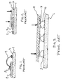
- Figure 1 shows a contact pad 3 formed on a chip 2 wire bonded to a corresponding contact pad 3 formed on a substrate 1.
- the contact pads 3 are electrically connected, or bonded, by a wire 4. Since the chip 2 typically has tens or even hundreds of the contact pads 3, wire bonding each contact pad 3 on the chip 2 to the corresponding contact pad 3 on the substrate 1 is labor intensive, expensive and slow. Further, the contact pads 3 must be large enough to accommodate both the wire 4 and the accuracy of the wire bonding device used to create the wire bond. Therefore, the contact pads 3 are made larger than otherwise necessary to compensate for the size limitations of the wire 4 and the wire bonding device.
- Figure 2 shows the contact pad 3 formed on the chip 2 tab bonded to the corresponding contact pad 3 on the substrate 1.
- a flexible substrate 5 having conductive lines formed on its lower surface is forced against the contact pads 3.
- a layer of anisotropic adhesive (not shown) is placed between the contact pads 3 and the flexible substrate 5. When the flexible substrate 5 is pressed against the contact pads 3, the anisotropic adhesive and the conductive lines formed on the flexible substrate 5 cooperate to complete the electrical connection between the contact pads 3.
- tab bonding suffers from yield loss, bond fragility, and high cost.
- FIG. 3 shows the chip 2 inverted with the contact pads 3 facing toward the substrate 1.
- the name "flip-chip” derives from the inversion of the chip 2, since the chip 2 is “flipped over” with the contacts pads 3 facing the substrate 1, in contrast to both tab bonding and wire bonding where the contact pads 3 on the chip 2 face away from the substrate 1. Note, however, that tab bonding can also be done with the chip 2 "flipped over”.
- solder bumps 6 are formed on the contact pads 3 on the substrate 1 or on the chip 2. The electrical connection between the corresponding contact pads 3 is completed by pressing the contact pads 3 on the chip 2 against the solder bumps 6 and melting the solder bumps 6.
- Flip-chip bonding is an improvement over both wire bonding and tab bonding.
- the relatively soft solder bumps 6 tend to permanently deform when the chip 2 is pressed down against the solder bumps 6. This deformation of the solder bumps 6 compensates for some irregularity in the heights of the contact pads 3 and any uneven contacting pressure forcing the chip 2 against the solder bumps 6.
- solder bumps 6 are not uniform in height or if the substrate 1 is warped, contact between the contact pads 3 and the solder bumps 6 can be broken. Also, if the contacting pressure forcing the chip 2 down on the solder bumps 6 is uneven, contact between some contact pads 3 and corresponding solder bumps 6 can fail. In addition, stresses from thermal expansion mismatches between the chip 2 and the substrate 1 can break the bonds formed by the solder bumps 6.
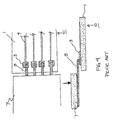
- Figure 4 shows a standard technique for establishing a temporary electrical contact between two devices.
- a probe card 7 having a plurality of probe needles 8 contacts the contact pads 3 by physically pressing the probe needles 8 against the contact pads 3.
- the physical contact between the probe needles 8 and the contact pads 3 creates an electrical connection between the probe needles 8 and the lines 9 formed on the substrate 1.
- the probe cards 7 are generally used to create only temporary contacts between the probe needles 8 and the contact pads 3, so that the device 10 can be tested, interrogated or otherwise communicated with.
- the device 10 can be a matrix of display electrodes which are part of an active-matrix liquid crystal display. Testing of the devices 10, such as liquid crystal display electrode matrices, is more thoroughly described in US-A-6531953.
- the probe cards 7 have many more applications than only for testing liquid crystal displays. Any device 10 having numerous and relatively small contact pads 3, similar to those found on the chip 2, can be tested using the probe card 7. However, standard techniques for producing the probe card 7 are time consuming and labor-intensive. Each probe card 7 must be custom-made for the particular device 10 to be tested. Typically, the probe needles 8 are manually formed on the probe card 7. Because the probe cards 7 are custom-made and relatively expensive, the probe cards 7 are not typically made to contact all of the contact pads 3 on the device 10 at one time. Therefore, only portions of the device 10 can be communicated with, tested or interrogated at any one time, requiring the probe card 7 be moved to allow communication, testing or interrogation of the entire device 10.
- the probe cards 7 are also used to test the chips 2 while the chips 2 are still part of a single-crystal silicon wafer.
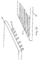
- One such probe card 7 is formed by photolithographic pattern plated processing, as disclosed in Probing at Die Level , Corwith, Advanced Packaging, February, 1995, pp. 26-28. Photolithographic pattern plated processing produces probe cards 7 which have essentially the same design as the standard probe card 7. However, this new type of processing appears to automate the method for producing probe needles 8, thus avoiding manually forming the probe needles 8. Also, this article discloses a probe card 7 which is bent at the end nearest the probe needles 8, as shown in Figure 5. The bend in the probe card 7 allows the probe needles 8 to contact the contact pad 3 at an angle.
- this invention provides a spring contact which exhibits the speed and ease of solder-bump flip-chip bonding while eliminating the need to create uniform solder bumps or uniform contacting pressure. Also, the invention provides finer-pitch contact arrays than solder-bump flip-chip bonding.
- a spring contact comprises a substrate, a contact surface disposed opposite the substrate; and an elastic member having an anchor portion and a free portion, the anchor portion being fixed to the substrate and the free portion being separated from the substrate; wherein elastic member comprises a plurality of layers with an inherent stress gradient in them which biases the free portion away from the substrate and in to contact with the surface disposed opposite the substrate
- This invention further provides a spring contact which has elastic properties enabling the spring contact to maintain physical contact with a contact pad despite variations in contact pad heights, contacting pressure, thermal variations or mechanical shock.
- This invention further provides a probe card and a method for producing the probe card having spring contacts in place of standard probe needles.
- Fig. 6 shows a side view of a bonding structure 100 having a plurality of spring contacts 15.
- Each spring contact 15 comprises a free portion 11 and an anchor portion 12 fixed to an insulating underlayer 13 and electrically connected to a contact pad 3.
- Each spring contact 15 is made of an extremely elastic material, such as a chrome-molybdenum alloy or a nickel-zirconium alloy.
- the spring contacts 15 are formed of an elastic conductive material, although they can be formed of a nonconductive or semi-conductive material if they are coated or plated with a conductor material. More preferably, the spring contacts 15 are formed of a nickel-Zirconium alloy having 1% zirconium. Zirconium is added to the nickel to improve the elastic properties of the alloy while not greatly reducing the conductivity of the nickel.
- the elastic material is not conductive, it is coated on at least one side with a conductive material, such as a metal or metal alloy.
- the contact pad 3 is the terminal end of a communication line which electrically communicates with an electronic device formed on the substrate 14 or device 101 such as a transistor, a display electrode, or other electrical device.
- the contact pad 3 is typically made of aluminum, but can be made of any conductive material. If the contact pad 3 on device 101 is made of aluminum, the contact pad 3 is preferably coated with a conductive material, such as gold, indium tin oxide, or nickel. This allows the spring contact 15 to make better electrical contact with the contact pad 3, since the spring contact 15 cannot "scrub" the uncoated contact pad 3 to break through the aluminum oxide that forms on an uncoated aluminum contact pad 3.
- the insulating underlayer 13 is made of silicon nitride or other etchable insulating material. However, the insulating underlayer 13 is not necessary and can be eliminated.
- the insulating underlayer 13 and the contact pad 3 are formed on or over a substrate 14, which is also formed of an insulating material, such as oxidized silicon or glass.
- a strip of metal having no stress gradient inherent in the metal will lie flat. However, as shown in Fig. 8, when the strip is bent into an arc, a uniform stress gradient ⁇ /h is introduced into the strip. Likewise, if a uniform stress gradient ⁇ /h is introduced into the flat metal strip, the metal strip will bend into an arc shape.
- Each spring contact 15 is formed such that a stress gradient ⁇ /h is introduced into the spring contact 15.
- the metal layer comprising the spring contact 15 is deposited such that compressive stress is present in upper portions of the metal layer and tensile stress is present in lower portions of the metal layer. Compressive stress in upper portions of the metal layer is depicted by arrows directed inwardly. Tensile stress is depicted in lower portions of the metal layer by arrows directed outwardly.
- the stress gradient ⁇ /h causes the spring contact 15 to bend into the shape of an arc having a radius r.
- Equation 1 gives the radius of curvature r of the spring contact 15: where Y is the Young's modulus of the metal, h is the thickness of the metal layer forming the spring contact 15, ⁇ is the total stress difference, and v is the Poisson's ratio of the metal.
- Equation 2 gives the approximate height b of the spring contact tip 30 from the substrate 14 for angles ⁇ ⁇ 50°: b ⁇ L 2 2r where L is the length of the free portion 11 and r is the radius of curvature of the free portion 11.
- each spring contact 15 is preferably made of a highly elastic material, each spring contact 15 can be pushed down at the tip 30 and deformed as shown in Fig. 6, but will not plastically deform.
- a contact pad 3 of a device 101 exerts the downward force placed on the tip 30 and electrically contacts the tip 30.
- the spring contact 15 resists the downward force placed on the tip 30 and maintains electrical contact with the contact pad 3.
- the spring contact When the force on the tip 30 is released, the spring contact will return to its undeformed state.
- the elasticity of the spring contacts 15 allows the spring contacts 15 to make numerous successive electrical connections with different contact pads 3 while maintaining the integrity of the electrical connection between the spring contact tip 30 and the contact pads 3.
- the spring contact 15 is preferably made of a creep-resistant material. Therefore, when the spring contact 15 is elastically deformed over an extended period by a contact pad 3 pressing down on the spring contact tip 30, the spring contact 15 resists the downward force and pushes the spring contact tip 30 against the contact pad 3, maintaining the electrical connection.
- the reaction force F tip of the tip 30 varies inversely with the distance x. Therefore, the reaction force F tip increases as the spring contact tip 30 gets closer to the substrate 14, since the distance x decreases as the spring contact 15 collapses and presses against the substrate 14 as shown in Fig. 6.
- the increase in the reaction force F tip as the contact pad 3 presses the spring contact tip 30 closer to the substrate 14 generally improves the electrical connection between the spring contact tip 30 and the contact pad 3.
- the increasing reaction force F tip causes the spring contact tip 30 and/or the contact pad 3 to deform locally at the area of contact, increasing the area of contact between the contact pad 3 and the spring contact tip 30.
- Figs. 10-13 show the basic steps in forming a spring contact 15.
- a contact pad 3 is formed on orovera substrate 14.
- an insulating underlayer 13 is formed on or over the substrate 14.
- the insulating underlayer 13 is not required and can be eliminated.
- a layer of metal 16 is deposited on or over the substrate 14.
- the metal is the nickel-zirconium alloy described above.
- Part of the metal layer 16 is electrically connected to or directly contacts the contact pad 3 and another portion of the metal layer 16 is deposited on or over the insulating underlayer 13.
- the metal layer 16 is sputter deposited.
- a plate of the metal When sputter-depositing a metal, a plate of the metal, called the target, is placed on a cathode, which is set to a high negative potential and immersed in a low-pressure gas, typically 1 to 100 millitorr, (0.13 to 133 Pa). This causes a glow-discharge plasma to ignite, from which positive ions are accelerated into the negatively charged target. This ion bombardment knocks metal atoms off the target, and many of these deposit on nearby surfaces, such as the substrate 14.
- a low-pressure gas typically 1 to 100 millitorr, (0.13 to 133 Pa).
- the metal layer 16 can be thought of as deposited in several sub-layers 16-1 to 16-n to a final thickness h of approximately 1 ⁇ m.
- the stress gradient ⁇ /h is introduced into the metal layer 16 by altering the stress inherent in each of the sub-layers 16-1 to 16-n of the metal layer 16, as shown in Fig. 11, each sub-layer 16-x having a different level of inherent stress.
- Different stress levels can be introduced into each sub-layer 16-x of the deposited metal layer 16 during sputter deposition in a variety of ways, including adding a reactive gas to the plasma; depositing the metal at an angle, and changing the pressure of the plasma gas.
- the different levels of stress are introduced into the metal layer 16 by varying the pressure of the plasma gas, which is preferably argon.
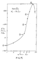
- Fig. 14 is a graph showing a typical relationship of the film stress in the sputter deposited nickel-zirconium alloy and the pressure of the plasma gas used in the deposition.
- the film stress in the deposited metal is compressive.
- the pressure of the plasma gas increases, the film stress in the deposited sub-layer changes to a tensile stress and increases with increasing plasma gas pressure.
- the metal layer 16 is deposited in five sub-layers 16-1 to 16-5.
- the first sub-layer 16-1 is deposited at a plasma gas pressure of 1 mTorr, as indicated by numeral 1 in Fig. 14.
- the first sub-layer 16-1 is the bottom-most layer in the metal layer 16 and has an inherent compressive stress.
- the second sub-layer 16-2 is deposited on top of the first sub-layer 16-1 at a plasma gas pressure of approximately 6 mTorr (1 Pa).
- the second sub-layer 16-2 has a slight inherent tensile stress, as indicated by numeral 2 in Fig. 14.
- Sub-layers 16-3, 16-4 and 16-5 are then deposited one on top of the other at the plasma gas pressures indicated by numerals 3, 4 and 5 in Fig. 14.
- the process of depositing the metal layer 16 in five separate sub-layers 16-1 to 16-5 results in the metal layer 16 having a stress gradient ⁇ /h which is compressive in the lower portion of the metal layer 16 and becomes increasingly tensile toward the top of the metal layer 16.
- the stress gradient ⁇ /h urges the metal layer 16 to bend into an arc, the metal layer 16 adheres to the insulating underlayer 13, the substrate 14 and the contact pad 3 and thus lies flat.
- the metal layer 16 is photolithographically patterned into the spring contacts 1 5.
- Photolithographic patterning is a well-known technique and is routinely used in the semiconductor chip industry.
- a positive photosensitive resist 17 is spun on top of the metal layer 16 and soft-baked at 90°C to drive off solvents in the resist 17.
- the photosensitive resist 17 is exposed to an appropriate pattern of ultraviolet light and then developed. Exposed areas of the resist 17 are removed during developing and the remaining resist 17 is hard-baked at 120°C.
- Wet or plasma etching is then used to remove the exposed areas of the metal layer 16.
- the remaining areas of the metal layer 16 after etching form the spring contacts 15.
- a top-view of one spring contact 15 is shown in Fig. 15. The area of the metal layer 16 removed by the etching is described by the dashed line 18.
- the free portion 11 of the spring contact 15 is released from the insulating underlayer 13 by a process of under-cut etching. Until the free portion 11 is released from the insulating underlayer 13, the free portion 11 adheres to the insulating underlayer 13 and the spring contact 15 lies flat on the substrate 14.
- the insulating underlayer 13 typically silicon nitride
- PECVD plasma chemical vapor deposition
- the insulating underlayer 13 is then pre-patterned, before the metal layer 16 is deposited, into islands on which the spring contacts 15 will be formed.
- the spring contacts 15 are released from the insulating underlayer 13 islands by etching the islands with a selective etchant.
- the selective etchant is typically a HF solution.
- the etchant is called a selective etchant because it etches the insulating underlayer 13 faster than the selective etchant removes metal from the spring contacts 15. This means that the spring contacts 15 are released from the insulating underlayer 13 and are allowed to bend up and away from the insulating underlayer 13 due to the stress gradient ⁇ /h in the spring contacts 15.
- the islands can also be formed of a low melting temperature material, such as solder or plastic. After the spring contacts 15 are formed, the low melting temperature material is heated to release the spring contacts 15.
- the insulating underlayer 13, if used, is not pre-patterned into islands. Instead, after the spring contacts 15 are formed, a passivating layer, such as silicon oxynitride, is deposited on the spring contacts 15 and the surrounding areas by PECVD. The passivation layer is patterned into windows, such as the shaded area shown in Fig. 15, to expose the free portion 11 of the spring contacts 15 and surrounding areas of the insulating underlayer 13. The same selective etchant, the HF solution, is used to etch the insulating underlayer 13 and release the spring contacts 15. This method avoids a step discontinuity in the metal of the spring contact 15 at the anchor portion 12 edge and leaves an insulating cover on the anchor portion 12. The insulating cover protects the anchor portion 12 from short-circuiting and also helps hold the anchor portion 12 down on the substrate 14.
- a passivating layer such as silicon oxynitride
- etchant vias or small windows, can be etched into the free portions 11 of the spring contacts 15.
- the etchant vias operate to provide the selective etchant faster access to the insulating underlayer 13, thereby speeding the process of releasing the free portions 11 from the insulating underlayer 13.
- a hard mask made of, for example, silicon, can be applied to the top surface of the spring contacts 15 to ensure that the etchant does not remove material from the top surface of the spring contacts 15 in case the photosensitive material 17 protecting the top of the spring contacts 15 fails during patterning of the spring contact 15.
- the stress gradient ⁇ /h causes the free portion 11 to bend up and away from the substrate 14.
- the stress gradient ⁇ /h is still inherent in the anchor portion 12 and urges the anchor portion 12 to pull away from the substrate 14.
- the spring contact 15 can be annealed to relieve the stress in the anchor portion 12. This annealing process does not affect the free portion 11 because, once the free portion 11 is released and allowed to bend up, no stress remains on the free portion 11 to be relieved by annealing. Thus, the free portion 11 remains curved up and away from the substrate 14 after annealing.
- Fig. 13 shows a layer of gold 19 plated over the outer surface of each spring contact 15.
- the layer of gold 19 is preferably used to reduce the resistance in the spring contacts 15, but can be replaced with any other conductive material.
- the gold layer 19 is plated on the spring contacts 15 using an electroless plating process.
- the process for forming the spring contacts 15 is limited only by the design rules of photolithographic patterning, many hundreds or thousands of spring contacts 15 can be formed closely together in a relatively small area on the substrate 14.
- the typical width w of the spring contact 15 is 10-100 ⁇ m. Therefore, the spring contacts 15 can be formed close together, at a spacing of approximately 10-20 ⁇ m. This makes the center-to-center distance between adjacent spring contacts 15 approximately 20-120 ⁇ m, which is within or less than the typical center-to-center distance between adjacent contact pads 3 on a standard semiconductor chip 2.
- a test array of the spring contacts 15 at a center-to-center spacing of 80 ⁇ m was developed as shown in Fig. 16.
- Four sets of arrays 20 of the spring contacts 15 were formed on a bottom substrate 21.
- Four corresponding arrays of linked contact pads 22 were formed on an upper substrate 23.
- the upper substrate 23 and the lower substrate 21 were brought together such that the spring contacts 15 contacted a corresponding contact pad 3.
- the resistance R was then measured across pairs of the spring contact 15 leads.
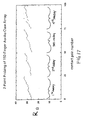
- Fig. 17 graphically depicts the measured resistance R for each spring contact pair in the test apparatus.
- the measured resistance R within each array generally trends upward from left to right because of the increased conductor length of the spring contacts 15 positioned to the right compared to the spring contacts 15 positioned to the left in each array. Most of the approximately 25-30 ohms of resistance measured for each spring contact 15 pair is due to the length and geometry of the conductors extending between the spring contacts 15 and the resistance R probing points.
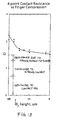
- Fig. 18 shows the total resistance of the connection between a spring contact 15 and corresponding contact pad 3 with most of the resistance R shown in Fig. 17 removed by using a 4-point probing geometry. As shown in Fig. 18, approximately 1.3 ohms of resistance is due to the conductors leading to the contact pad 3 and the spring contact 15. Approximately 0.2 ohms of resistance is due to the shape of the spring contact tip 30. The remaining resistance, approximately 0.1 ohms for b ⁇ 80 ⁇ m, is the resistance at the interface between the contact pad 3 and the spring contact tip 30.
- the resistance at the interface between the contact pad 3 and the spring contact tip 30 decreases as the height b decreases.
- the reaction force F tip that the spring contact tip 30 exerts against the contact pad 3 increases as the contact pad 3 pushes the spring contact tip 30 closer to the substrate 14.
- the increased reaction force F tip causes the spring contact tip 30 to locally deform at the contact pad 3, thereby increasing the contact area and decreasing the resistance at the interface.
- the shape of the spring contact tip 30 can take different forms, depending on the application. Since the spring contacts 15 are photolithographically patterned, the spring contact tips 30 are easily formed in a variety of shapes.
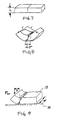
- Fig. 19 shows a spring contact tip 30 having a flat end.
- the spring contact tip 30 shown in Fig. 20 has a pointed end which concentrates the force F tip exerted by the spring contact 15 at a single point on the contact pad 3. This pointed shape aids the spring contact tip 30 when breaking through some oxides which may be present on the contact pads 3.
- Figs. 21 and 22 show spring contact tips 30 having multiple points for applications where contact redundancy is required.
- Fig. 23 shows a spring contact tip 30 having a deformable tab. The deformable tab increases the contact area with the contact pad 3, by deforming as shown in Fig. 24 when the spring contact 15 forces the tip 30 against the contact pad 3.
- the spring contact tips 30 can be ultrasonically scrubbed into the contact pads 3 to increase the area of contact. Also, the spring contact tips 30 and the contact pads 3 can be coated with solder which is melted after the tips 30 and the contact pads 3 are brought into contact. Melting the solder bonds the spring contacts 15 to the contact pads 3.
- Fig. 25 shows one preferred embodiment of the invention.
- the spring contacts 15 are formed on the lower surface of the chip 2.
- the spring contacts 15 contact corresponding contact pads 3 on the substrate 14.
- the adhesive 24 holds the chip 2 stationary with respect to substrate 14.
- Fig. 26 shows the substrate 14 having a plurality of spring contacts 15 formed on the top surface of the substrate 14.
- the contact pads 3 formed on the lower surface of the chip 2 are electrically connected to corresponding spring contacts 15 on the substrate 14.
- An adhesive 24 holds the chip 2 stationary relative to a dust cover, or can, 25 covering the chip 2 and hermetically seals the dust cover 25 to the substrate 14.
- the dust cover 25 assures that moisture and other foreign substances do not corrode the spring contacts 15 or the contact pads 3, or otherwise interfere with the electrical connections between the individual spring contacts 15 and the corresponding contact pads 3.
- Optional cooling fins 50 and the dust cover 25 provide a heat sink to cool the chip 2.
- Fig. 27 shows an alternate form of the embodiment shown in Fig. 26.
- the adhesive 24 holds the chip 2 stationary to the substrate 14. No heat sink is provided by the dust cover 25.
- Fig. 28 shows an alternate embodiment of a connecting device for electrically connecting two devices.
- a wafer 26 is shown having a plurality of spring contacts 15 formed on opposite sides of the wafer. Pairs of the spring contacts 15 on opposite sides of the wafer 26 communicate with each other by way of vias etched in the wafer 26 and electrically connect the contact pads 3 on both the chip 2 and the substrate 14.
- This embodiment of the invention allows processing of the chip 2 and the substrate 14 without risking damage to the spring contacts 15.
- the wafer 26 is used to interconnect the chip 2 and the substrate 14 only after all processing is completed on the chip 2 and the substrate 14.
- the spring contacts 15 are not limited to interconnecting a chip 2 to a substrate 14 or circuit board.
- the spring contacts 15 are used equally well to interconnect two chips 2, two circuit boards, or other electronic devices to each other. Two exemplary applications are mounting driver chips to visual displays and assembling multi-chip modules (MCM's) for computers.
- MCM's multi-chip modules
- Another alternative use for the spring contacts 15 is in probe cards. As discussed above, probe cards 7 are used to temporarily connect two devices, typically when one of the devices is tested. Such testing is common in the semiconductor industry, where the probe cards 7 are used to test semiconductor chips while the chips are still part of a single-crystal silicon wafer.
- Fig. 29 shows an embodiment of the invention where the probe card 27 has an array of spring contacts 15 used in place of the standard probe needles 8.
- the probe card 27 operates identically to the standard probe card 7 except for having spring contacts 15.
- the probe card 27 is aligned with the device 10 such that the spring contacts 15 compliantly contact the corresponding contact pads 3 on the device 10.
- the device 10 is then tested or communicated with by a testing device electrically connected to the probe card 27.
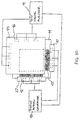
- a display pattern generator 40 communicates with driver chips 42 mounted on the two full-width probe cards 27.
- the probe cards 27 have the spring contacts 15 which contact associated addressing lines 43 formed on the display plate 44.
- the addressing lines 43 communicate with display electrodes (not shown). Therefore, the display pattern generator 40 can drive the display electrodes to produce a matrix of electric potentials corresponding to a test image.
- Sensors (not shown) on the sensor plate 45 detect the matrix of electric potentials on the display electrodes and generate signals each corresponding to the electric potential. The signals are read out by scanner chips 46 mounted on the sensor plate 45.
- the test signal analyzer 41 receives the signals from the scanner chips 46 and forms a sensed image corresponding to the signals. The test signal analyzer 41 then compares the sensed image with the test image output by the display pattern generator 40 to determine if the display plate 44 and display electrodes are working properly.
- probe card 27 Since producing a standard probe card 7 having probe needles 8 is labor intensive and time-consuming, standard probe cards 7 are not generally made to contact all of the addressing lines 43 on the display plate 44. Therefore, testing of the display plate 44 must be done in sections since the probe cards 7 cannot accommodate the full width of the addressing lines 43. In contrast, the probe card 27 made with spring contacts 15 can be made easily and inexpensively. Also, the probe cards 27 having the spring contacts 15 can be made to any width and therefore can test all of the data or address lines of an apparatus, such as the display shown in Fig. 30, at one time.
- wafer-scale testing and burning-in of chips 2 can be performed by a single probe card 27 contacting all contact pads 3 of all chips 2 while the chips 2 are still part of a single semiconductor wafer.
- the probe card 27 can be a silicon wafer containing microcircuitry to distribute test signals to and from each chip 2 on the wafer under test. The test signals can be distributed either all at once or sequentially to the chips 2.
Description
- This invention generally relates to photolithographically-patterned spring contacts for use in electrically bonding integrated circuits, circuit boards, electrode arrays, or other devices.
- Standard bonding techniques for electrically connecting integrated circuits, or chips, to a circuit board or other device include wire bonding, tab bonding, solder-bump and gold-bump flip-chip bonding and other techniques. Figure 1 shows a contact pad 3 formed on a chip 2 wire bonded to a corresponding contact pad 3 formed on a substrate 1. The contact pads 3 are electrically connected, or bonded, by a wire 4. Since the chip 2 typically has tens or even hundreds of the contact pads 3, wire bonding each contact pad 3 on the chip 2 to the corresponding contact pad 3 on the substrate 1 is labor intensive, expensive and slow. Further, the contact pads 3 must be large enough to accommodate both the wire 4 and the accuracy of the wire bonding device used to create the wire bond. Therefore, the contact pads 3 are made larger than otherwise necessary to compensate for the size limitations of the wire 4 and the wire bonding device.
- Figure 2 shows the contact pad 3 formed on the chip 2 tab bonded to the corresponding contact pad 3 on the substrate 1. A flexible substrate 5 having conductive lines formed on its lower surface is forced against the contact pads 3. A layer of anisotropic adhesive (not shown) is placed between the contact pads 3 and the flexible substrate 5. When the flexible substrate 5 is pressed against the contact pads 3, the anisotropic adhesive and the conductive lines formed on the flexible substrate 5 cooperate to complete the electrical connection between the contact pads 3. Like wire bonding, tab bonding suffers from yield loss, bond fragility, and high cost.
- Another conventional method for bonding the contact pads 3 formed on the chip 2 to the contact pads 3 formed on the substrate 1 or to some other device is solder-bump flip-chip bonding. Figure 3 shows the chip 2 inverted with the contact pads 3 facing toward the substrate 1. The name "flip-chip" derives from the inversion of the chip 2, since the chip 2 is "flipped over" with the contacts pads 3 facing the substrate 1, in contrast to both tab bonding and wire bonding where the contact pads 3 on the chip 2 face away from the substrate 1. Note, however, that tab bonding can also be done with the chip 2 "flipped over". In standard flip-chip bonding, solder bumps 6 are formed on the contact pads 3 on the substrate 1 or on the chip 2. The electrical connection between the corresponding contact pads 3 is completed by pressing the contact pads 3 on the chip 2 against the solder bumps 6 and melting the solder bumps 6.
- Flip-chip bonding is an improvement over both wire bonding and tab bonding. The relatively soft solder bumps 6 tend to permanently deform when the chip 2 is pressed down against the solder bumps 6. This deformation of the solder bumps 6 compensates for some irregularity in the heights of the contact pads 3 and any uneven contacting pressure forcing the chip 2 against the solder bumps 6.
- However, flip-chip bonding does suffer from both mechanical and thermal variations in the solder bumps 6. If the solder bumps 6 are not uniform in height or if the substrate 1 is warped, contact between the contact pads 3 and the solder bumps 6 can be broken. Also, if the contacting pressure forcing the chip 2 down on the solder bumps 6 is uneven, contact between some contact pads 3 and corresponding solder bumps 6 can fail. In addition, stresses from thermal expansion mismatches between the chip 2 and the substrate 1 can break the bonds formed by the solder bumps 6.
- In contrast to the relatively permanent bonds described above, Figure 4 shows a standard technique for establishing a temporary electrical contact between two devices. A probe card 7 having a plurality of probe needles 8 contacts the contact pads 3 by physically pressing the probe needles 8 against the contact pads 3. The physical contact between the probe needles 8 and the contact pads 3 creates an electrical connection between the probe needles 8 and the lines 9 formed on the substrate 1.
- The probe cards 7 are generally used to create only temporary contacts between the probe needles 8 and the contact pads 3, so that the device 10 can be tested, interrogated or otherwise communicated with. The device 10 can be a matrix of display electrodes which are part of an active-matrix liquid crystal display. Testing of the devices 10, such as liquid crystal display electrode matrices, is more thoroughly described in US-A-6531953.
- The probe cards 7 have many more applications than only for testing liquid crystal displays. Any device 10 having numerous and relatively small contact pads 3, similar to those found on the chip 2, can be tested using the probe card 7. However, standard techniques for producing the probe card 7 are time consuming and labor-intensive. Each probe card 7 must be custom-made for the particular device 10 to be tested. Typically, the probe needles 8 are manually formed on the probe card 7. Because the probe cards 7 are custom-made and relatively expensive, the probe cards 7 are not typically made to contact all of the contact pads 3 on the device 10 at one time. Therefore, only portions of the device 10 can be communicated with, tested or interrogated at any one time, requiring the probe card 7 be moved to allow communication, testing or interrogation of the entire device 10.
- The probe cards 7 are also used to test the chips 2 while the chips 2 are still part of a single-crystal silicon wafer. One such probe card 7 is formed by photolithographic pattern plated processing, as disclosed in Probing at Die Level, Corwith, Advanced Packaging, February, 1995, pp. 26-28. Photolithographic pattern plated processing produces probe cards 7 which have essentially the same design as the standard probe card 7. However, this new type of processing appears to automate the method for producing probe needles 8, thus avoiding manually forming the probe needles 8. Also, this article discloses a probe card 7 which is bent at the end nearest the probe needles 8, as shown in Figure 5. The bend in the probe card 7 allows the probe needles 8 to contact the contact pad 3 at an angle. As the probe card 7 pushes the probe needles 8 into the contact pads 3, a mechanical scrubbing action occurs which allows the probe needles 8 to break through the oxide formed on the top surface of the contact pad 3. All of the standard probe cards 7, however,are limited to testing contact pads 3 which are arranged in a linear array.
- Accordingly, this invention provides a spring contact which exhibits the speed and ease of solder-bump flip-chip bonding while eliminating the need to create uniform solder bumps or uniform contacting pressure. Also, the invention provides finer-pitch contact arrays than solder-bump flip-chip bonding.
- According to this invention a spring contact comprises a substrate,
a contact surface disposed opposite the substrate; and
an elastic member having an anchor portion and a free portion, the anchor portion being fixed to the substrate and the free portion being separated from the substrate;
wherein elastic member comprises a plurality of layers with an inherent stress gradient in them which biases the free portion away from the substrate and in to contact with the surface disposed opposite the substrate - This invention further provides a spring contact which has elastic properties enabling the spring contact to maintain physical contact with a contact pad despite variations in contact pad heights, contacting pressure, thermal variations or mechanical shock.
- This invention further provides a probe card and a method for producing the probe card having spring contacts in place of standard probe needles.
- This invention will be described in relation to the following drawings, in which reference numerals refer to like elements and wherein:
- Fig. 1 shows a chip wire bonded to a substrate;
- Fig. 2 shows the chip tab bonded to the substrate;
- Fig. 3 shows the chip solder-bump flip-chip bonded to the substrate;
- Fig. 4 shows a probe card contacting an electronic device;
- Fig. 5 shows a probe card having an angled probe needle;
- Fig. 6 is a spring contact in an undeformed free state and another spring contact deformed when contacting a contact pad;
- Fig. 7 shows a metal strip with no stress gradient;
- Fig. 8 shows a model for determining the curvature of a spring contact due to the stress gradient;
- Fig. 9 shows a model for determining the amount of reaction force exerted at the tip of the spring contact;
- Fig. 10 shows the first steps in a method of forming a spring contact according to the invention;
- Fig. 11 shows additional steps following those shown in Fig. 10 in a method of forming a spring contact according to the invention;
- Fig. 12 shows additional steps following those shown in Fig. 11 in a method of forming a spring contact according to the invention;
- Fig. 13 shows a final step in one of the methods of forming a spring contact according to the invention;
- Fig. 14 is a graphic representation of the film stress in a sputter deposited nickel-zirconium alloy as a function of plasma gas pressure;
- Fig. 15 is a top view of a spring contact;
- Fig. 16 is a device for testing the contact resistance of a plurality of spring contact pairs;
- Fig. 17 is a graphical representation of the detected resistance of a plurality of spring contact pairs;
- Fig. 18 is a graphic representation of the contact resistance of a spring contact as a function of the distance between the contact pad and the substrate;
- Fig. 19 is a spring contact having a flat end;
- Fig. 20 is a spring contact having a pointed end;
- Fig. 21 is a spring contact having two points at the tip end;
- Fig. 22 is a spring contact having multiple points at the tip end;
- Fig. 23 is a spring contact having a deformable tab at the tip end;
- Fig. 24 shows a spring contact having a deformed tab end when forced against a contact pad;
- Fig. 25 is a chip having a plurality of spring contacts electrically bonded to a substrate;
- Fig. 26 is a chip bonded to a dust cover and electrically contacted to a substrate having a plurality of spring contacts and a dust cover;
- Fig. 26 is a chip bonded to a dust cover and electrically contacted to a substrate having a plurality of spring contacts;
- Fig. 27 is a chip bonded to a substrate and electrically contacted to a plurality of spring contacts on the substrate;
- Fig. 28 is a chip electrically bonded to a substrate by way of an intermediate wafer having a plurality of spring contacts;
- Fig. 29 is a probe card having a plurality of spring contacts used for testing an electronic device; and
- Fig. 30 is a liquid crystal display and a device for testing the operation of the display.
-
- Fig. 6 shows a side view of a bonding structure 100 having a plurality of spring contacts 15. Each spring contact 15 comprises a free portion 11 and an anchor portion 12 fixed to an insulating underlayer 13 and electrically connected to a contact pad 3. Each spring contact 15 is made of an extremely elastic material, such as a chrome-molybdenum alloy or a nickel-zirconium alloy. Preferably, the spring contacts 15 are formed of an elastic conductive material, although they can be formed of a nonconductive or semi-conductive material if they are coated or plated with a conductor material. More preferably, the spring contacts 15 are formed of a nickel-Zirconium alloy having 1% zirconium. Zirconium is added to the nickel to improve the elastic properties of the alloy while not greatly reducing the conductivity of the nickel. When the elastic material is not conductive, it is coated on at least one side with a conductive material, such as a metal or metal alloy.
- The contact pad 3 is the terminal end of a communication line which electrically communicates with an electronic device formed on the substrate 14 or device 101 such as a transistor, a display electrode, or other electrical device. The contact pad 3 is typically made of aluminum, but can be made of any conductive material. If the contact pad 3 on device 101 is made of aluminum, the contact pad 3 is preferably coated with a conductive material, such as gold, indium tin oxide, or nickel. This allows the spring contact 15 to make better electrical contact with the contact pad 3, since the spring contact 15 cannot "scrub" the uncoated contact pad 3 to break through the aluminum oxide that forms on an uncoated aluminum contact pad 3. The insulating underlayer 13 is made of silicon nitride or other etchable insulating material. However, the insulating underlayer 13 is not necessary and can be eliminated. The insulating underlayer 13 and the contact pad 3 are formed on or over a substrate 14, which is also formed of an insulating material, such as oxidized silicon or glass.
- As shown in Fig. 7, a strip of metal having no stress gradient inherent in the metal will lie flat. However, as shown in Fig. 8, when the strip is bent into an arc, a uniform stress gradient Δσ/h is introduced into the strip. Likewise, if a uniform stress gradient Δσ/h is introduced into the flat metal strip, the metal strip will bend into an arc shape.
- Each spring contact 15 is formed such that a stress gradient Δσ/h is introduced into the spring contact 15. When the spring contact 15 is formed, the metal layer comprising the spring contact 15 is deposited such that compressive stress is present in upper portions of the metal layer and tensile stress is present in lower portions of the metal layer. Compressive stress in upper portions of the metal layer is depicted by arrows directed inwardly. Tensile stress is depicted in lower portions of the metal layer by arrows directed outwardly. The stress gradient Δσ/h causes the spring contact 15 to bend into the shape of an arc having a radius r. Equation 1 gives the radius of curvature r of the spring contact 15:where Y is the Young's modulus of the metal, h is the thickness of the metal layer forming the spring contact 15, Δσ is the total stress difference, and v is the Poisson's ratio of the metal.

- Referring again to Fig. 6, r is the radius of curvature of the free portion 11 of the spring contact 15 as predicted in Equation 1, and Θ is the angle separating the radius line directed toward the junction of the free portion 11 with the anchor portion 12 and the radius line directed toward the tip 30 of the free portion 11. Equation 2 gives the approximate height b of the spring contact tip 30 from the substrate 14 for angles Θ < 50°:
- Since each spring contact 15 is preferably made of a highly elastic material, each spring contact 15 can be pushed down at the tip 30 and deformed as shown in Fig. 6, but will not plastically deform. Typically, a contact pad 3 of a device 101 exerts the downward force placed on the tip 30 and electrically contacts the tip 30. The spring contact 15 resists the downward force placed on the tip 30 and maintains electrical contact with the contact pad 3.
- When the force on the tip 30 is released, the spring contact will return to its undeformed state. Thus, the elasticity of the spring contacts 15 allows the spring contacts 15 to make numerous successive electrical connections with different contact pads 3 while maintaining the integrity of the electrical connection between the spring contact tip 30 and the contact pads 3.
- Additionally, the spring contact 15 is preferably made of a creep-resistant material. Therefore, when the spring contact 15 is elastically deformed over an extended period by a contact pad 3 pressing down on the spring contact tip 30, the spring contact 15 resists the downward force and pushes the spring contact tip 30 against the contact pad 3, maintaining the electrical connection.
- Fig. 9 shows a model for determining the amount of force Ftip applied by the spring contact tip 30 to a contact pad 3 in reaction to the force of the contact pad 3 pressing down on the spring contact tip 30. Equation 3 gives the reaction force Ftip of the spring contact tip 30:
- For a given width w, thickness h and stress difference Δσ, the reaction force Ftip of the tip 30 varies inversely with the distance x. Therefore, the reaction force Ftip increases as the spring contact tip 30 gets closer to the substrate 14, since the distance x decreases as the spring contact 15 collapses and presses against the substrate 14 as shown in Fig. 6. The increase in the reaction force Ftip as the contact pad 3 presses the spring contact tip 30 closer to the substrate 14 generally improves the electrical connection between the spring contact tip 30 and the contact pad 3. The increasing reaction force Ftip causes the spring contact tip 30 and/or the contact pad 3 to deform locally at the area of contact, increasing the area of contact between the contact pad 3 and the spring contact tip 30.
- Figs. 10-13 show the basic steps in forming a spring contact 15. In Fig. 10, a contact pad 3 is formed on orovera substrate 14. Additionally, an insulating underlayer 13 is formed on or over the substrate 14. However, as mentioned above, the insulating underlayer 13 is not required and can be eliminated.
- In Fig. 11, a layer of metal 16 is deposited on or over the substrate 14. In the preferred embodiment of the invention, the metal is the nickel-zirconium alloy described above. Part of the metal layer 16 is electrically connected to or directly contacts the contact pad 3 and another portion of the metal layer 16 is deposited on or over the insulating underlayer 13. There are many methods available for depositing a metal layer 16 on or over the substrate 14, including electron-beam deposition, thermal evaporation, chemical vapor deposition, sputter deposition and other methods. Preferably, the metal layer 16 is sputter deposited.
- When sputter-depositing a metal, a plate of the metal, called the target, is placed on a cathode, which is set to a high negative potential and immersed in a low-pressure gas, typically 1 to 100 millitorr, (0.13 to 133 Pa). This causes a glow-discharge plasma to ignite, from which positive ions are accelerated into the negatively charged target. This ion bombardment knocks metal atoms off the target, and many of these deposit on nearby surfaces, such as the substrate 14.
- The metal layer 16 can be thought of as deposited in several sub-layers 16-1 to 16-n to a final thickness h of approximately 1 µm. The stress gradient Δ/h is introduced into the metal layer 16 by altering the stress inherent in each of the sub-layers 16-1 to 16-n of the metal layer 16, as shown in Fig. 11, each sub-layer 16-x having a different level of inherent stress.
- Different stress levels can be introduced into each sub-layer 16-x of the deposited metal layer 16 during sputter deposition in a variety of ways, including adding a reactive gas to the plasma; depositing the metal at an angle, and changing the pressure of the plasma gas. Preferably, the different levels of stress are introduced into the metal layer 16 by varying the pressure of the plasma gas, which is preferably argon.
- Fig. 14 is a graph showing a typical relationship of the film stress in the sputter deposited nickel-zirconium alloy and the pressure of the plasma gas used in the deposition. For low pressures of the plasma gas, approximately 1 mTorr (0.13 Pa), the film stress in the deposited metal is compressive. As the pressure of the plasma gas increases, the film stress in the deposited sub-layer changes to a tensile stress and increases with increasing plasma gas pressure.
- Preferably, the metal layer 16 is deposited in five sub-layers 16-1 to 16-5. The first sub-layer 16-1 is deposited at a plasma gas pressure of 1 mTorr, as indicated by numeral 1 in Fig. 14. The first sub-layer 16-1 is the bottom-most layer in the metal layer 16 and has an inherent compressive stress. The second sub-layer 16-2 is deposited on top of the first sub-layer 16-1 at a plasma gas pressure of approximately 6 mTorr (1 Pa). The second sub-layer 16-2 has a slight inherent tensile stress, as indicated by numeral 2 in Fig. 14. Sub-layers 16-3, 16-4 and 16-5 are then deposited one on top of the other at the plasma gas pressures indicated by numerals 3, 4 and 5 in Fig. 14.
- The process of depositing the metal layer 16 in five separate sub-layers 16-1 to 16-5 results in the metal layer 16 having a stress gradient Δ/h which is compressive in the lower portion of the metal layer 16 and becomes increasingly tensile toward the top of the metal layer 16. Although the stress gradient Δ/h urges the metal layer 16 to bend into an arc, the metal layer 16 adheres to the insulating underlayer 13, the substrate 14 and the contact pad 3 and thus lies flat.
- After the metal layer 16 is deposited, the metal layer 16 is photolithographically patterned into the spring contacts 1 5. Photolithographic patterning is a well-known technique and is routinely used in the semiconductor chip industry. First, a positive photosensitive resist 17 is spun on top of the metal layer 16 and soft-baked at 90°C to drive off solvents in the resist 17. The photosensitive resist 17 is exposed to an appropriate pattern of ultraviolet light and then developed. Exposed areas of the resist 17 are removed during developing and the remaining resist 17 is hard-baked at 120°C. Wet or plasma etching is then used to remove the exposed areas of the metal layer 16. The remaining areas of the metal layer 16 after etching form the spring contacts 15. A top-view of one spring contact 15 is shown in Fig. 15. The area of the metal layer 16 removed by the etching is described by the dashed line 18.
- Next, as shown in Fig. 12, the free portion 11 of the spring contact 15 is released from the insulating underlayer 13 by a process of under-cut etching. Until the free portion 11 is released from the insulating underlayer 13, the free portion 11 adheres to the insulating underlayer 13 and the spring contact 15 lies flat on the substrate 14. There are two methods for releasing the spring contacts 15 from the substrate 14 or insulating underlayer 13. In the first method, the insulating underlayer 13, typically silicon nitride, is deposited by plasma chemical vapor deposition (PECVD) at a temperature of 200-250°C. This gives the insulating underlayer 13 a fast etch rate. The insulating underlayer 13 is then pre-patterned, before the metal layer 16 is deposited, into islands on which the spring contacts 15 will be formed. After the spring contacts 15 are formed on or over the islands of the insulating underlayer 13, the spring contacts 15 are released from the insulating underlayer 13 islands by etching the islands with a selective etchant. The selective etchant is typically a HF solution. The etchant is called a selective etchant because it etches the insulating underlayer 13 faster than the selective etchant removes metal from the spring contacts 15. This means that the spring contacts 15 are released from the insulating underlayer 13 and are allowed to bend up and away from the insulating underlayer 13 due to the stress gradient Δσ/h in the spring contacts 15. The islands can also be formed of a low melting temperature material, such as solder or plastic. After the spring contacts 15 are formed, the low melting temperature material is heated to release the spring contacts 15.
- In the second method for releasing the spring contacts 15, the insulating underlayer 13, if used, is not pre-patterned into islands. Instead, after the spring contacts 15 are formed, a passivating layer, such as silicon oxynitride, is deposited on the spring contacts 15 and the surrounding areas by PECVD. The passivation layer is patterned into windows, such as the shaded area shown in Fig. 15, to expose the free portion 11 of the spring contacts 15 and surrounding areas of the insulating underlayer 13. The same selective etchant, the HF solution, is used to etch the insulating underlayer 13 and release the spring contacts 15. This method avoids a step discontinuity in the metal of the spring contact 15 at the anchor portion 12 edge and leaves an insulating cover on the anchor portion 12. The insulating cover protects the anchor portion 12 from short-circuiting and also helps hold the anchor portion 12 down on the substrate 14.
- Only those areas of the insulating underlayer 13 under the free portion 11 of the spring contact 15 are under-cut etched. The area of insulating underlayer 13 under-cut etched for each spring contact 15 is described by the shaded portion in Fig. 15. This means that the anchor portion 12 of the spring contact 15 remains fixed to the insulating underlayer 13 and does not pull away from the insulating underlayer 13. It should be appreciated that the method for patterning the metal layer 16 into the spring contacts 15 should not result in any annealing of the metal layer 16.
- Additional steps can be added to the under-cut etching processes to improve the processes if necessary. For example, etchant vias, or small windows, can be etched into the free portions 11 of the spring contacts 15. The etchant vias operate to provide the selective etchant faster access to the insulating underlayer 13, thereby speeding the process of releasing the free portions 11 from the insulating underlayer 13. Also, a hard mask, made of, for example, silicon, can be applied to the top surface of the spring contacts 15 to ensure that the etchant does not remove material from the top surface of the spring contacts 15 in case the photosensitive material 17 protecting the top of the spring contacts 15 fails during patterning of the spring contact 15.
- Once the free portion 11 is freed from the insulating underlayer 13, the stress gradient Δσ/h causes the free portion 11 to bend up and away from the substrate 14. The stress gradient Δσ/h is still inherent in the anchor portion 12 and urges the anchor portion 12 to pull away from the substrate 14.
- To decrease the chance of the anchor portion 12 pulling away from the substrate 14, the spring contact 15 can be annealed to relieve the stress in the anchor portion 12. This annealing process does not affect the free portion 11 because, once the free portion 11 is released and allowed to bend up, no stress remains on the free portion 11 to be relieved by annealing. Thus, the free portion 11 remains curved up and away from the substrate 14 after annealing.
- Finally, Fig. 13 shows a layer of gold 19 plated over the outer surface of each spring contact 15. The layer of gold 19 is preferably used to reduce the resistance in the spring contacts 15, but can be replaced with any other conductive material. Preferably, the gold layer 19 is plated on the spring contacts 15 using an electroless plating process.
- Since the process for forming the spring contacts 15 is limited only by the design rules of photolithographic patterning, many hundreds or thousands of spring contacts 15 can be formed closely together in a relatively small area on the substrate 14. The typical width w of the spring contact 15 is 10-100 µm. Therefore, the spring contacts 15 can be formed close together, at a spacing of approximately 10-20 µm. This makes the center-to-center distance between adjacent spring contacts 15 approximately 20-120 µm, which is within or less than the typical center-to-center distance between adjacent contact pads 3 on a standard semiconductor chip 2.
- To test the effectiveness of the spring contacts 15 in applications similar to those found in solder-bump flip-chip bonding, a test array of the spring contacts 15 at a center-to-center spacing of 80 µm was developed as shown in Fig. 16. Four sets of arrays 20 of the spring contacts 15 were formed on a bottom substrate 21. Four corresponding arrays of linked contact pads 22 were formed on an upper substrate 23. The upper substrate 23 and the lower substrate 21 were brought together such that the spring contacts 15 contacted a corresponding contact pad 3. The resistance R was then measured across pairs of the spring contact 15 leads.
- Fig. 17 graphically depicts the measured resistance R for each spring contact pair in the test apparatus. The measured resistance R within each array generally trends upward from left to right because of the increased conductor length of the spring contacts 15 positioned to the right compared to the spring contacts 15 positioned to the left in each array. Most of the approximately 25-30 ohms of resistance measured for each spring contact 15 pair is due to the length and geometry of the conductors extending between the spring contacts 15 and the resistance R probing points.
- Fig. 18 shows the total resistance of the connection between a spring contact 15 and corresponding contact pad 3 with most of the resistance R shown in Fig. 17 removed by using a 4-point probing geometry. As shown in Fig. 18, approximately 1.3 ohms of resistance is due to the conductors leading to the contact pad 3 and the spring contact 15. Approximately 0.2 ohms of resistance is due to the shape of the spring contact tip 30. The remaining resistance, approximately 0.1 ohms for b<80 µm, is the resistance at the interface between the contact pad 3 and the spring contact tip 30.
- In general, the resistance at the interface between the contact pad 3 and the spring contact tip 30 decreases as the height b decreases. As mentioned above, the reaction force Ftip that the spring contact tip 30 exerts against the contact pad 3 increases as the contact pad 3 pushes the spring contact tip 30 closer to the substrate 14. The increased reaction force Ftip causes the spring contact tip 30 to locally deform at the contact pad 3, thereby increasing the contact area and decreasing the resistance at the interface.
- The shape of the spring contact tip 30 can take different forms, depending on the application. Since the spring contacts 15 are photolithographically patterned, the spring contact tips 30 are easily formed in a variety of shapes. Fig. 19 shows a spring contact tip 30 having a flat end. The spring contact tip 30 shown in Fig. 20 has a pointed end which concentrates the force Ftip exerted by the spring contact 15 at a single point on the contact pad 3. This pointed shape aids the spring contact tip 30 when breaking through some oxides which may be present on the contact pads 3. Figs. 21 and 22 show spring contact tips 30 having multiple points for applications where contact redundancy is required. Fig. 23 shows a spring contact tip 30 having a deformable tab. The deformable tab increases the contact area with the contact pad 3, by deforming as shown in Fig. 24 when the spring contact 15 forces the tip 30 against the contact pad 3.
- Other methods are used to lower the contact resistance between the spring contact tip 30 and the contact pad 3. The spring contact tips 30 can be ultrasonically scrubbed into the contact pads 3 to increase the area of contact. Also, the spring contact tips 30 and the contact pads 3 can be coated with solder which is melted after the tips 30 and the contact pads 3 are brought into contact. Melting the solder bonds the spring contacts 15 to the contact pads 3.
- As mentioned above, since the production of the spring contacts 15 is limited only by the design rules of photolithographic patterning, the spring contacts 15 can be used to interconnect numerous different types of devices. For example, Fig. 25 shows one preferred embodiment of the invention. The spring contacts 15 are formed on the lower surface of the chip 2. The spring contacts 15 contact corresponding contact pads 3 on the substrate 14. The adhesive 24 holds the chip 2 stationary with respect to substrate 14. Fig. 26 shows the substrate 14 having a plurality of spring contacts 15 formed on the top surface of the substrate 14. The contact pads 3 formed on the lower surface of the chip 2 are electrically connected to corresponding spring contacts 15 on the substrate 14. An adhesive 24 holds the chip 2 stationary relative to a dust cover, or can, 25 covering the chip 2 and hermetically seals the dust cover 25 to the substrate 14. The dust cover 25 assures that moisture and other foreign substances do not corrode the spring contacts 15 or the contact pads 3, or otherwise interfere with the electrical connections between the individual spring contacts 15 and the corresponding contact pads 3. Optional cooling fins 50 and the dust cover 25 provide a heat sink to cool the chip 2. Fig. 27 shows an alternate form of the embodiment shown in Fig. 26. The adhesive 24 holds the chip 2 stationary to the substrate 14. No heat sink is provided by the dust cover 25.
- Fig. 28 shows an alternate embodiment of a connecting device for electrically connecting two devices. A wafer 26 is shown having a plurality of spring contacts 15 formed on opposite sides of the wafer. Pairs of the spring contacts 15 on opposite sides of the wafer 26 communicate with each other by way of vias etched in the wafer 26 and electrically connect the contact pads 3 on both the chip 2 and the substrate 14. This embodiment of the invention allows processing of the chip 2 and the substrate 14 without risking damage to the spring contacts 15. The wafer 26 is used to interconnect the chip 2 and the substrate 14 only after all processing is completed on the chip 2 and the substrate 14.
- The spring contacts 15 are not limited to interconnecting a chip 2 to a substrate 14 or circuit board. The spring contacts 15 are used equally well to interconnect two chips 2, two circuit boards, or other electronic devices to each other. Two exemplary applications are mounting driver chips to visual displays and assembling multi-chip modules (MCM's) for computers. Another alternative use for the spring contacts 15 is in probe cards. As discussed above, probe cards 7 are used to temporarily connect two devices, typically when one of the devices is tested. Such testing is common in the semiconductor industry, where the probe cards 7 are used to test semiconductor chips while the chips are still part of a single-crystal silicon wafer.
- Fig. 29 shows an embodiment of the invention where the probe card 27 has an array of spring contacts 15 used in place of the standard probe needles 8. The probe card 27 operates identically to the standard probe card 7 except for having spring contacts 15. The probe card 27 is aligned with the device 10 such that the spring contacts 15 compliantly contact the corresponding contact pads 3 on the device 10. The device 10 is then tested or communicated with by a testing device electrically connected to the probe card 27.
- An example testing device is shown in Fig. 30 which is more thoroughly described in the application JAO 34053 filed concurrently herewith. A display pattern generator 40 communicates with driver chips 42 mounted on the two full-width probe cards 27. The probe cards 27 have the spring contacts 15 which contact associated addressing lines 43 formed on the display plate 44. The addressing lines 43 communicate with display electrodes (not shown). Therefore, the display pattern generator 40 can drive the display electrodes to produce a matrix of electric potentials corresponding to a test image. Sensors (not shown) on the sensor plate 45 detect the matrix of electric potentials on the display electrodes and generate signals each corresponding to the electric potential. The signals are read out by scanner chips 46 mounted on the sensor plate 45. The test signal analyzer 41 receives the signals from the scanner chips 46 and forms a sensed image corresponding to the signals. The test signal analyzer 41 then compares the sensed image with the test image output by the display pattern generator 40 to determine if the display plate 44 and display electrodes are working properly.
- Since producing a standard probe card 7 having probe needles 8 is labor intensive and time-consuming, standard probe cards 7 are not generally made to contact all of the addressing lines 43 on the display plate 44. Therefore, testing of the display plate 44 must be done in sections since the probe cards 7 cannot accommodate the full width of the addressing lines 43. In contrast, the probe card 27 made with spring contacts 15 can be made easily and inexpensively. Also, the probe cards 27 having the spring contacts 15 can be made to any width and therefore can test all of the data or address lines of an apparatus, such as the display shown in Fig. 30, at one time.
- In another example, wafer-scale testing and burning-in of chips 2 can be performed by a single probe card 27 contacting all contact pads 3 of all chips 2 while the chips 2 are still part of a single semiconductor wafer. The probe card 27 can be a silicon wafer containing microcircuitry to distribute test signals to and from each chip 2 on the wafer under test. The test signals can be distributed either all at once or sequentially to the chips 2.
- While the invention has been described with reference to specific embodiments, the description of the specific embodiments is illustrative only and is not to be construed as limiting the scope of the invention. Various other modifications and changes may occur to those skilled in the art without departing from the scope of the invention as set forth in the following claims.
Claims (10)
- A spring contact, comprising:wherein elastic member (15) comprises a plurality of layers with an inherent stress gradient in them which biases the free portion away from the substrate and in to contact with the surface (3) disposed opposite the substrate (14).a substrate (14),a contact surface (3) disposed opposite the substrate; andan elastic member (15) having an anchor portion (12) and a free portion (11), the anchor portion (12) being fixed to the substrate and the free portion (11) being separated from the substrate;
- A spring contact according to claim 1, wherein the anchor portion (12) is electrically connected to a first contact (3) formed over the substrate (14) and the free portion (11) compliantly contacts the contact surface (3) formed over a second substrate (101).
- A probe card and a device being probed, comprising:a substrate (14) forming part of the probe;a plurality of conductive signal lines formed on the substrate; anda plurality of spring contacts in accordance with claim 1 or 2 arranged in a pattern matching an array of contact pads (3) on the device to be probed disposed opposite the substrate (14), each of the plurality of spring contacts electrically contacting a corresponding one of the plurality of conductive signal lines.
- A probe card and device according to claim 3, wherein:the device to be probed is a visual display matrix, and each one of the plurality of spring contacts (15) makes contact with a corresponding contact pad (3) of the array of contact pads, andselected ones of a plurality of display electrodes of the visual display matrix, communicating with at least one of the plurality of conductive signal lines, are activated.
- A probe card and device according to claim 3, wherein the device to be probed is a semiconductor wafer comprising a plurality of chips and the array of contact pads, each of the plurality of chips undergoing one of wafer-scale testing and burning-in.
- A contacting device, comprising:a substrate (14) having a top side and an opposite bottom side;at least one top spring contact (15) in accordance with claim 1 or 2 formed on the top side of the substrate (14), the at least one top spring contact being arranged to match and contact a corresponding at least one contact pad (3) on a first device above the substance; andat least one bottom spring contact (15) in accordance with claim 1 or 2 formed on the bottom side of the substrate (14), the at least one bottom spring contact arranged to match and contact a corresponding at least one contact pad (3) on a second device below the substrate, each at least one bottom spring contact (15) electrically communicating with a corresponding one of the at least one top spring contact (15).
- The spring contact, probe card or contacting device according to any of the preceding claims, wherein (A) the or each elastic member (15) is formed of an electrically conductive material, or (B) an electrically conductive layer is formed on at least a portion of an outer surface of the or each elastic member (15).
- A spring contact, probe card and device or contacting device according to any of the preceding claims, wherein a free end of the free portion (11) of the or each of the plurality of spring contacts (15) is coated with a material softer than a material forming the or each of the plurality of spring contacts, the softer material improving contact between the free end of each of the plurality of spring contacts and the corresponding contact pads (3).
- A method for forming a spring contact according to claim 1, comprising the steps of:depositing a layer of an elastic material on a substrate (14), the elastic material having an inherent stress gradient, the inherent stress gradient biasing the elastic material away from the substrate;photolithographically patterning the layer of elastic material to form at least one spring contact (15) having a free portion (11) and an anchor portion (12), andunder-cut etching a portion of the substrate (14) under the at least one spring contact (15) to release the free portion (11) of the at least one spring contact from the substrate, and the anchor portion (12) of the at least one spring contact remaining fixed to the substrate wherein the free portion is biased to move away from the substrate by the inherent stress gradient when the free portion is released to contact a surface which is positioned opposite the substrate.
- The method of claim 9, wherein the step of under-cut etching comprises the steps of:photolithographically forming etchant vias into the at least one spring contact (15), andapplying an etchant to etch the substrate (14) under the at least one spring contact (15) to release the free portion (11) of the spring contact from the substrate, and preferably wherein the step of depositing the layer of the elastic material comprises the step of sputter depositing a plurality of sub-layers of a metal alloy, each of the plurality of sub-layers deposited at a different selected plasma gas pressure, each different selected plasma gas pressure creating a corresponding different level of inherent stress in a corresponding one of the plurality of sub-layers.
Applications Claiming Priority (3)
| Application Number | Priority Date | Filing Date | Title |
|---|---|---|---|
| US08/478,578 US5613861A (en) | 1995-06-07 | 1995-06-07 | Photolithographically patterned spring contact |
| US478578 | 1995-06-07 | ||
| PCT/US1996/008018 WO1996041506A1 (en) | 1995-06-07 | 1996-05-30 | Photolithographically patterned spring contact |
Publications (3)
| Publication Number | Publication Date |
|---|---|
| EP0834243A1 EP0834243A1 (en) | 1998-04-08 |
| EP0834243A4 EP0834243A4 (en) | 1998-08-12 |
| EP0834243B1 true EP0834243B1 (en) | 2004-09-08 |
Family
ID=23900491
Family Applications (1)
| Application Number | Title | Priority Date | Filing Date |
|---|---|---|---|
| EP96916778A Expired - Lifetime EP0834243B1 (en) | 1995-06-07 | 1996-05-30 | Photolithographically patterned spring contact |
Country Status (7)
| Country | Link |
|---|---|
| US (6) | US5613861A (en) |
| EP (1) | EP0834243B1 (en) |
| JP (1) | JP3795922B2 (en) |
| KR (1) | KR100442902B1 (en) |
| DE (1) | DE69633334T2 (en) |
| ES (1) | ES2227588T3 (en) |
| WO (1) | WO1996041506A1 (en) |
Families Citing this family (248)
| Publication number | Priority date | Publication date | Assignee | Title |
|---|---|---|---|---|
| US5476211A (en) * | 1993-11-16 | 1995-12-19 | Form Factor, Inc. | Method of manufacturing electrical contacts, using a sacrificial member |
| US5917707A (en) | 1993-11-16 | 1999-06-29 | Formfactor, Inc. | Flexible contact structure with an electrically conductive shell |
| US7200930B2 (en) * | 1994-11-15 | 2007-04-10 | Formfactor, Inc. | Probe for semiconductor devices |
| US6482013B2 (en) | 1993-11-16 | 2002-11-19 | Formfactor, Inc. | Microelectronic spring contact element and electronic component having a plurality of spring contact elements |
| US20030199179A1 (en) * | 1993-11-16 | 2003-10-23 | Formfactor, Inc. | Contact tip structure for microelectronic interconnection elements and method of making same |
| US20020053734A1 (en) | 1993-11-16 | 2002-05-09 | Formfactor, Inc. | Probe card assembly and kit, and methods of making same |
| US7579269B2 (en) * | 1993-11-16 | 2009-08-25 | Formfactor, Inc. | Microelectronic spring contact elements |
| US6727580B1 (en) | 1993-11-16 | 2004-04-27 | Formfactor, Inc. | Microelectronic spring contact elements |
| US6690186B2 (en) | 1994-07-07 | 2004-02-10 | Tessera, Inc. | Methods and structures for electronic probing arrays |
| US6499216B1 (en) | 1994-07-07 | 2002-12-31 | Tessera, Inc. | Methods and structures for electronic probing arrays |
| US20100065963A1 (en) * | 1995-05-26 | 2010-03-18 | Formfactor, Inc. | Method of wirebonding that utilizes a gas flow within a capillary from which a wire is played out |
| US5613861A (en) | 1995-06-07 | 1997-03-25 | Xerox Corporation | Photolithographically patterned spring contact |
| KR100202998B1 (en) * | 1995-12-02 | 1999-06-15 | 남재우 | Wafer probe card having a micro-tip and manufacturing method thereof |
| JP2908747B2 (en) * | 1996-01-10 | 1999-06-21 | 三菱電機株式会社 | IC socket |
| US8033838B2 (en) | 1996-02-21 | 2011-10-11 | Formfactor, Inc. | Microelectronic contact structure |
| JP3022312B2 (en) * | 1996-04-15 | 2000-03-21 | 日本電気株式会社 | Method of manufacturing probe card |
| JP3215629B2 (en) * | 1996-07-12 | 2001-10-09 | シャープ株式会社 | Recording head |
| US5907817A (en) * | 1996-12-24 | 1999-05-25 | Ericsson Inc. | Radiotelephones with coplanar antenna connectors and related assembly methods |
| US6520778B1 (en) | 1997-02-18 | 2003-02-18 | Formfactor, Inc. | Microelectronic contact structures, and methods of making same |
| US5923178A (en) * | 1997-04-17 | 1999-07-13 | Cerprobe Corporation | Probe assembly and method for switchable multi-DUT testing of integrated circuit wafers |
| US6045396A (en) * | 1997-09-12 | 2000-04-04 | Trw Inc. | Flex cable connector for cryogenic application |
| US6245444B1 (en) | 1997-10-02 | 2001-06-12 | New Jersey Institute Of Technology | Micromachined element and method of fabrication thereof |
| US6357112B1 (en) * | 1997-11-25 | 2002-03-19 | Tessera, Inc. | Method of making connection component |
| US5944537A (en) * | 1997-12-15 | 1999-08-31 | Xerox Corporation | Photolithographically patterned spring contact and apparatus and methods for electrically contacting devices |
| US6807734B2 (en) * | 1998-02-13 | 2004-10-26 | Formfactor, Inc. | Microelectronic contact structures, and methods of making same |
| US5979892A (en) * | 1998-05-15 | 1999-11-09 | Xerox Corporation | Controlled cilia for object manipulation |
| EP1095282B1 (en) * | 1998-07-08 | 2007-09-19 | Capres Aps | Multi-point probe |
| US6441315B1 (en) * | 1998-11-10 | 2002-08-27 | Formfactor, Inc. | Contact structures with blades having a wiping motion |
| US6491968B1 (en) | 1998-12-02 | 2002-12-10 | Formfactor, Inc. | Methods for making spring interconnect structures |
| TW589453B (en) * | 1998-12-02 | 2004-06-01 | Formfactor Inc | Lithographic contact elements |
| US6672875B1 (en) * | 1998-12-02 | 2004-01-06 | Formfactor, Inc. | Spring interconnect structures |
| US6255126B1 (en) * | 1998-12-02 | 2001-07-03 | Formfactor, Inc. | Lithographic contact elements |
| US6627483B2 (en) * | 1998-12-04 | 2003-09-30 | Formfactor, Inc. | Method for mounting an electronic component |
| US6456099B1 (en) | 1998-12-31 | 2002-09-24 | Formfactor, Inc. | Special contact points for accessing internal circuitry of an integrated circuit |
| US6183267B1 (en) | 1999-03-11 | 2001-02-06 | Murray Hill Devices | Ultra-miniature electrical contacts and method of manufacture |
| US6498636B1 (en) * | 1999-03-30 | 2002-12-24 | National Semiconductor Corporation | Apparatus and method for substantially stress-free electrical connection to a liquid crystal display |
| EP1183604A2 (en) * | 1999-05-27 | 2002-03-06 | Nanonexus, Inc. | Test interface for electronic circuirts |
| US7126220B2 (en) * | 2002-03-18 | 2006-10-24 | Nanonexus, Inc. | Miniaturized contact spring |
| US20070245553A1 (en) * | 1999-05-27 | 2007-10-25 | Chong Fu C | Fine pitch microfabricated spring contact structure & method |
| US6710609B2 (en) * | 2002-07-15 | 2004-03-23 | Nanonexus, Inc. | Mosaic decal probe |
| US7382142B2 (en) | 2000-05-23 | 2008-06-03 | Nanonexus, Inc. | High density interconnect system having rapid fabrication cycle |
| WO2001098793A2 (en) * | 2000-06-20 | 2001-12-27 | Nanonexus, Inc. | Systems for testing integraged circuits during burn-in |
| US6799976B1 (en) | 1999-07-28 | 2004-10-05 | Nanonexus, Inc. | Construction structures and manufacturing processes for integrated circuit wafer probe card assemblies |
| US6812718B1 (en) * | 1999-05-27 | 2004-11-02 | Nanonexus, Inc. | Massively parallel interface for electronic circuits |
| US7247035B2 (en) * | 2000-06-20 | 2007-07-24 | Nanonexus, Inc. | Enhanced stress metal spring contactor |
| EP1200843A1 (en) * | 1999-07-28 | 2002-05-02 | Nanonexus, Inc. | Construction structures and manufacturing processes for integrated circuit wafer probe card assemblies |
| US7189077B1 (en) * | 1999-07-30 | 2007-03-13 | Formfactor, Inc. | Lithographic type microelectronic spring structures with improved contours |
| US6939474B2 (en) * | 1999-07-30 | 2005-09-06 | Formfactor, Inc. | Method for forming microelectronic spring structures on a substrate |
| US6713374B2 (en) | 1999-07-30 | 2004-03-30 | Formfactor, Inc. | Interconnect assemblies and methods |
| WO2001009952A2 (en) * | 1999-07-30 | 2001-02-08 | Formfactor, Inc. | Interconnect assemblies and methods |
| US7435108B1 (en) * | 1999-07-30 | 2008-10-14 | Formfactor, Inc. | Variable width resilient conductive contact structures |
| US6888362B2 (en) * | 2000-11-09 | 2005-05-03 | Formfactor, Inc. | Test head assembly for electronic components with plurality of contoured microelectronic spring contacts |
| US6780001B2 (en) * | 1999-07-30 | 2004-08-24 | Formfactor, Inc. | Forming tool for forming a contoured microelectronic spring mold |
| US6426233B1 (en) * | 1999-08-03 | 2002-07-30 | Micron Technology, Inc. | Uniform emitter array for display devices, etch mask for the same, and methods for making the same |
| US6297562B1 (en) * | 1999-09-20 | 2001-10-02 | Telefonaktieboalget Lm Ericsson (Publ) | Semiconductive chip having a bond pad located on an active device |
| US6352454B1 (en) * | 1999-10-20 | 2002-03-05 | Xerox Corporation | Wear-resistant spring contacts |
| US6267605B1 (en) | 1999-11-15 | 2001-07-31 | Xerox Corporation | Self positioning, passive MEMS mirror structures |
| US6213789B1 (en) * | 1999-12-15 | 2001-04-10 | Xerox Corporation | Method and apparatus for interconnecting devices using an adhesive |
| US6794725B2 (en) | 1999-12-21 | 2004-09-21 | Xerox Corporation | Amorphous silicon sensor with micro-spring interconnects for achieving high uniformity in integrated light-emitting sources |
| US6426637B1 (en) | 1999-12-21 | 2002-07-30 | Cerprobe Corporation | Alignment guide and signal transmission apparatus and method for spring contact probe needles |
| US6827584B2 (en) * | 1999-12-28 | 2004-12-07 | Formfactor, Inc. | Interconnect for microelectronic structures with enhanced spring characteristics |
| US6586955B2 (en) | 2000-03-13 | 2003-07-01 | Tessera, Inc. | Methods and structures for electronic probing arrays |
| US7262611B2 (en) * | 2000-03-17 | 2007-08-28 | Formfactor, Inc. | Apparatuses and methods for planarizing a semiconductor contactor |
| JP4323055B2 (en) * | 2000-03-22 | 2009-09-02 | 富士通マイクロエレクトロニクス株式会社 | Semiconductor device testing contactor and method of manufacturing the same |
| US6367251B1 (en) * | 2000-04-05 | 2002-04-09 | Jds Uniphase Corporation | Lockable microelectromechanical actuators using thermoplastic material, and methods of operating same |
| US6640432B1 (en) * | 2000-04-12 | 2003-11-04 | Formfactor, Inc. | Method of fabricating shaped springs |
| US7458816B1 (en) | 2000-04-12 | 2008-12-02 | Formfactor, Inc. | Shaped spring |
| US6856225B1 (en) * | 2000-05-17 | 2005-02-15 | Xerox Corporation | Photolithographically-patterned out-of-plane coil structures and method of making |
| US6392524B1 (en) | 2000-06-09 | 2002-05-21 | Xerox Corporation | Photolithographically-patterned out-of-plane coil structures and method of making |
| US6396677B1 (en) * | 2000-05-17 | 2002-05-28 | Xerox Corporation | Photolithographically-patterned variable capacitor structures and method of making |
| JP3650722B2 (en) * | 2000-05-18 | 2005-05-25 | 株式会社アドバンテスト | Probe card and manufacturing method thereof |
| US7952373B2 (en) | 2000-05-23 | 2011-05-31 | Verigy (Singapore) Pte. Ltd. | Construction structures and manufacturing processes for integrated circuit wafer probe card assemblies |
| US7579848B2 (en) * | 2000-05-23 | 2009-08-25 | Nanonexus, Inc. | High density interconnect system for IC packages and interconnect assemblies |
| US20050068054A1 (en) * | 2000-05-23 | 2005-03-31 | Sammy Mok | Standardized layout patterns and routing structures for integrated circuit wafer probe card assemblies |
| EP1168510B1 (en) * | 2000-06-21 | 2004-09-01 | Itt Manufacturing Enterprises, Inc. | Electrical connecting device |
| US6505811B1 (en) * | 2000-06-27 | 2003-01-14 | Kelsey-Hayes Company | High-pressure fluid control valve assembly having a microvalve device attached to fluid distributing substrate |
| US6290510B1 (en) | 2000-07-27 | 2001-09-18 | Xerox Corporation | Spring structure with self-aligned release material |
| US6504643B1 (en) * | 2000-09-28 | 2003-01-07 | Xerox Corporation | Structure for an optical switch on a substrate |
| US6632373B1 (en) * | 2000-09-28 | 2003-10-14 | Xerox Corporation | Method for an optical switch on a substrate |
| US6632374B1 (en) * | 2000-09-28 | 2003-10-14 | Xerox Corporation | Method for an optical switch on a silicon on insulator substrate |
| DE60116969T2 (en) * | 2000-09-28 | 2006-07-27 | Xerox Corp. | Production of a mirror structure |
| WO2002087024A1 (en) * | 2000-10-18 | 2002-10-31 | Honeywell International Inc. | Compliant interposer for single-sided electronic package attachment |
| US6377438B1 (en) * | 2000-10-23 | 2002-04-23 | Mcnc | Hybrid microelectromechanical system tunable capacitor and associated fabrication methods |
| US6743982B2 (en) | 2000-11-29 | 2004-06-01 | Xerox Corporation | Stretchable interconnects using stress gradient films |
| US6655964B2 (en) | 2001-02-09 | 2003-12-02 | Xerox Corporation | Low cost integrated out-of-plane micro-device structures and method of making |
| US6595787B2 (en) * | 2001-02-09 | 2003-07-22 | Xerox Corporation | Low cost integrated out-of-plane micro-device structures and method of making |
| US6534249B2 (en) | 2001-02-09 | 2003-03-18 | Xerox Corporation | Method of making low cost integrated out-of-plane micro-device structures |
| US6910268B2 (en) * | 2001-03-27 | 2005-06-28 | Formfactor, Inc. | Method for fabricating an IC interconnect system including an in-street integrated circuit wafer via |
| US6811406B2 (en) | 2001-04-12 | 2004-11-02 | Formfactor, Inc. | Microelectronic spring with additional protruding member |
| US6528350B2 (en) | 2001-05-21 | 2003-03-04 | Xerox Corporation | Method for fabricating a metal plated spring structure |
| US6730134B2 (en) | 2001-07-02 | 2004-05-04 | Intercon Systems, Inc. | Interposer assembly |
| US6560861B2 (en) * | 2001-07-11 | 2003-05-13 | Xerox Corporation | Microspring with conductive coating deposited on tip after release |
| US6729019B2 (en) * | 2001-07-11 | 2004-05-04 | Formfactor, Inc. | Method of manufacturing a probe card |
| US6713956B2 (en) * | 2001-07-24 | 2004-03-30 | Lite-On Technology Corporation | Display module including a plate for heat dissipation and shielding |
| US7153399B2 (en) * | 2001-08-24 | 2006-12-26 | Nanonexus, Inc. | Method and apparatus for producing uniform isotropic stresses in a sputtered film |
| US6664885B2 (en) * | 2001-08-31 | 2003-12-16 | Adc Telecommunications, Inc. | Thermally activated latch |
| US6625004B1 (en) * | 2001-08-31 | 2003-09-23 | Superconductor Technologies, Inc. | Electrostatic actuators with intrinsic stress gradient |
| US6731492B2 (en) * | 2001-09-07 | 2004-05-04 | Mcnc Research And Development Institute | Overdrive structures for flexible electrostatic switch |
| US6794737B2 (en) * | 2001-10-12 | 2004-09-21 | Xerox Corporation | Spring structure with stress-balancing layer |
| JP2003168736A (en) * | 2001-11-30 | 2003-06-13 | Hitachi Ltd | Semiconductor element, high-frequency power amplifier and radio communication set |
| DE10159415B4 (en) * | 2001-12-04 | 2012-10-04 | MAX-PLANCK-Gesellschaft zur Förderung der Wissenschaften e.V. | Method for producing a microcoil and microcoil |
| ITMI20012574A1 (en) * | 2001-12-06 | 2003-06-06 | Technoprobe S R L | CONTACT PROBE FOR A MEASUREMENT HEAD |
| DE10162983B4 (en) | 2001-12-20 | 2010-07-08 | Qimonda Ag | Contact spring arrangement for the electrical contacting of a semiconductor wafer for test purposes and method for its production |
| US7064953B2 (en) * | 2001-12-27 | 2006-06-20 | Formfactor, Inc. | Electronic package with direct cooling of active electronic components |
| US6891385B2 (en) | 2001-12-27 | 2005-05-10 | Formfactor, Inc. | Probe card cooling assembly with direct cooling of active electronic components |
| US6684499B2 (en) | 2002-01-07 | 2004-02-03 | Xerox Corporation | Method for fabricating a spring structure |
| US6756244B2 (en) * | 2002-01-29 | 2004-06-29 | Hewlett-Packard Development Company, L.P. | Interconnect structure |
| DE10210344A1 (en) * | 2002-03-08 | 2003-10-02 | Univ Bremen | Method for producing micromechanical components and components produced using the method |
| US6668628B2 (en) | 2002-03-29 | 2003-12-30 | Xerox Corporation | Scanning probe system with spring probe |
| US6866255B2 (en) * | 2002-04-12 | 2005-03-15 | Xerox Corporation | Sputtered spring films with low stress anisotropy |
| US7006720B2 (en) * | 2002-04-30 | 2006-02-28 | Xerox Corporation | Optical switching system |
| US6891240B2 (en) | 2002-04-30 | 2005-05-10 | Xerox Corporation | Electrode design and positioning for controlled movement of a moveable electrode and associated support structure |
| US20060053625A1 (en) * | 2002-05-07 | 2006-03-16 | Microfabrica Inc. | Microprobe tips and methods for making |
| US20060051948A1 (en) * | 2003-02-04 | 2006-03-09 | Microfabrica Inc. | Microprobe tips and methods for making |
| US7412767B2 (en) * | 2003-02-04 | 2008-08-19 | Microfabrica, Inc. | Microprobe tips and methods for making |
| US7363705B2 (en) * | 2003-02-04 | 2008-04-29 | Microfabrica, Inc. | Method of making a contact |
| US7273812B2 (en) * | 2002-05-07 | 2007-09-25 | Microfabrica Inc. | Microprobe tips and methods for making |
| US7265565B2 (en) | 2003-02-04 | 2007-09-04 | Microfabrica Inc. | Cantilever microprobes for contacting electronic components and methods for making such probes |
| DE10221085B4 (en) * | 2002-05-11 | 2012-07-26 | Robert Bosch Gmbh | Assembly having a connection device for contacting a semiconductor device and manufacturing method |
| US7011530B2 (en) * | 2002-05-24 | 2006-03-14 | Sitaraman Suresh K | Multi-axis compliance spring |
| US20040000579A1 (en) * | 2002-07-01 | 2004-01-01 | Fuerst Robert M. | Forming contact arrays on substrates |
| US6621141B1 (en) | 2002-07-22 | 2003-09-16 | Palo Alto Research Center Incorporated | Out-of-plane microcoil with ground-plane structure |
| US8080221B2 (en) * | 2002-08-05 | 2011-12-20 | Palo Alto Research Center Incorporated | Capillary-channel probes for liquid pickup, transportation and dispense using stressy metal |
| US7241420B2 (en) * | 2002-08-05 | 2007-07-10 | Palo Alto Research Center Incorporated | Capillary-channel probes for liquid pickup, transportation and dispense using stressy metal |
| US20040100638A1 (en) * | 2002-11-27 | 2004-05-27 | The Regents Of The University Of California. | Correcting surface contour of a non-rigid object through control of surface residual stress |
| US20080211524A1 (en) * | 2003-02-04 | 2008-09-04 | Microfabrica Inc. | Electrochemically Fabricated Microprobes |
| US20080106280A1 (en) * | 2003-02-04 | 2008-05-08 | Microfabrica Inc. | Vertical Microprobes for Contacting Electronic Components and Method for Making Such Probes |
| US10416192B2 (en) | 2003-02-04 | 2019-09-17 | Microfabrica Inc. | Cantilever microprobes for contacting electronic components |
| US7056131B1 (en) * | 2003-04-11 | 2006-06-06 | Neoconix, Inc. | Contact grid array system |
| US20100167561A1 (en) * | 2003-04-11 | 2010-07-01 | Neoconix, Inc. | Structure and process for a contact grid array formed in a circuitized substrate |
| US20070020960A1 (en) * | 2003-04-11 | 2007-01-25 | Williams John D | Contact grid array system |
| US7244125B2 (en) * | 2003-12-08 | 2007-07-17 | Neoconix, Inc. | Connector for making electrical contact at semiconductor scales |
| US8584353B2 (en) * | 2003-04-11 | 2013-11-19 | Neoconix, Inc. | Method for fabricating a contact grid array |
| US6916181B2 (en) * | 2003-06-11 | 2005-07-12 | Neoconix, Inc. | Remountable connector for land grid array packages |
| US7628617B2 (en) * | 2003-06-11 | 2009-12-08 | Neoconix, Inc. | Structure and process for a contact grid array formed in a circuitized substrate |
| US20050120553A1 (en) * | 2003-12-08 | 2005-06-09 | Brown Dirk D. | Method for forming MEMS grid array connector |
| US7113408B2 (en) * | 2003-06-11 | 2006-09-26 | Neoconix, Inc. | Contact grid array formed on a printed circuit board |
| US7597561B2 (en) * | 2003-04-11 | 2009-10-06 | Neoconix, Inc. | Method and system for batch forming spring elements in three dimensions |
| US7114961B2 (en) * | 2003-04-11 | 2006-10-03 | Neoconix, Inc. | Electrical connector on a flexible carrier |
| US7758351B2 (en) * | 2003-04-11 | 2010-07-20 | Neoconix, Inc. | Method and system for batch manufacturing of spring elements |
| US6869290B2 (en) * | 2003-06-11 | 2005-03-22 | Neoconix, Inc. | Circuitized connector for land grid array |
| US7070419B2 (en) * | 2003-06-11 | 2006-07-04 | Neoconix Inc. | Land grid array connector including heterogeneous contact elements |
| US7015584B2 (en) * | 2003-07-08 | 2006-03-21 | Xerox Corporation | High force metal plated spring structure |
| US20050012212A1 (en) * | 2003-07-17 | 2005-01-20 | Cookson Electronics, Inc. | Reconnectable chip interface and chip package |
| US6844214B1 (en) | 2003-08-21 | 2005-01-18 | Xerox, Corporation | Microelectromechanical system based sensors, sensor arrays, sensing systems, sensing methods and methods of fabrication |
| US7030632B2 (en) * | 2003-10-14 | 2006-04-18 | Micron Technology, Inc. | Compliant contract structures, contactor cards and test system including same |
| US6973722B2 (en) * | 2003-11-17 | 2005-12-13 | Palo Alto Research Center Incorporated | Release height adjustment of stressy metal devices by annealing before and after release |
| JP4182430B2 (en) * | 2003-11-28 | 2008-11-19 | オムロン株式会社 | Transmitter |
| US6998703B2 (en) | 2003-12-04 | 2006-02-14 | Palo Alto Research Center Inc. | Thin package for stacking integrated circuits |
| US20050227510A1 (en) * | 2004-04-09 | 2005-10-13 | Brown Dirk D | Small array contact with precision working range |
| US7160121B2 (en) * | 2003-12-15 | 2007-01-09 | Palo Alto Research Center Incorporated | Stressed metal contact with enhanced lateral compliance |
| US7410590B2 (en) * | 2003-12-19 | 2008-08-12 | Palo Alto Research Center Incorporated | Transferable micro spring structure |
| US20080108221A1 (en) * | 2003-12-31 | 2008-05-08 | Microfabrica Inc. | Microprobe Tips and Methods for Making |
| US6912082B1 (en) | 2004-03-11 | 2005-06-28 | Palo Alto Research Center Incorporated | Integrated driver electronics for MEMS device using high voltage thin film transistors |
| TWI286606B (en) * | 2004-03-16 | 2007-09-11 | Gunsei Kimoto | Electric signal connecting device, and probe assembly and prober device using it |
| US7383632B2 (en) * | 2004-03-19 | 2008-06-10 | Neoconix, Inc. | Method for fabricating a connector |
| US7090503B2 (en) * | 2004-03-19 | 2006-08-15 | Neoconix, Inc. | Interposer with compliant pins |
| US7025601B2 (en) * | 2004-03-19 | 2006-04-11 | Neoconix, Inc. | Interposer and method for making same |
| US20050205988A1 (en) * | 2004-03-19 | 2005-09-22 | Epic Technology Inc. | Die package with higher useable die contact pad area |
| US7347698B2 (en) * | 2004-03-19 | 2008-03-25 | Neoconix, Inc. | Deep drawn electrical contacts and method for making |
| US7651382B2 (en) * | 2006-12-01 | 2010-01-26 | Interconnect Portfolio Llc | Electrical interconnection devices incorporating redundant contact points for reducing capacitive stubs and improved signal integrity |
| US7192320B2 (en) * | 2004-03-26 | 2007-03-20 | Silicon Pipe, Inc. | Electrical interconnection devices incorporating redundant contact points for reducing capacitive stubs and improved signal integrity |
| US7695053B1 (en) * | 2004-04-16 | 2010-04-13 | Bae Systems Survivability Systems, Llc | Lethal threat protection system for a vehicle and method |
| EP1738217A4 (en) * | 2004-04-23 | 2009-12-16 | Res Triangle Inst | Flexible electrostatic actuator |
| US7372013B2 (en) * | 2004-04-27 | 2008-05-13 | California Institute Of Technology | Near field scanning microscope probe and method for fabricating same |
| US7454095B2 (en) * | 2004-04-27 | 2008-11-18 | California Institute Of Technology | Integrated plasmon and dielectric waveguides |
| US20050277281A1 (en) * | 2004-06-10 | 2005-12-15 | Dubin Valery M | Compliant interconnect and method of formation |
| WO2008070673A2 (en) * | 2006-12-04 | 2008-06-12 | Nanonexus, Inc. | Construction structures and manufacturing processes for integrated circuit wafer probe card assemblies |
| US7649145B2 (en) * | 2004-06-18 | 2010-01-19 | Micron Technology, Inc. | Compliant spring contact structures |
| US20060000642A1 (en) * | 2004-07-01 | 2006-01-05 | Epic Technology Inc. | Interposer with compliant pins |
| US7354276B2 (en) * | 2004-07-20 | 2008-04-08 | Neoconix, Inc. | Interposer with compliant pins |
| US7156365B2 (en) * | 2004-07-27 | 2007-01-02 | Kelsey-Hayes Company | Method of controlling microvalve actuator |
| US7082684B2 (en) * | 2004-08-04 | 2006-08-01 | Palo Alto Research Center Incorporated | Intermetallic spring structure |
| US20060030179A1 (en) * | 2004-08-05 | 2006-02-09 | Palo Alto Research Center, Incorporated | Transmission-line spring structure |
| JP5219512B2 (en) * | 2004-08-09 | 2013-06-26 | トランスフォーム・ソーラー・ピーティーワイ・リミテッド | Solar cell (elongated small piece) submodule structure |
| US7750487B2 (en) * | 2004-08-11 | 2010-07-06 | Intel Corporation | Metal-metal bonding of compliant interconnect |
| US6956389B1 (en) * | 2004-08-16 | 2005-10-18 | Jem America Corporation | Highly resilient cantilever spring probe for testing ICs |
| US7459795B2 (en) * | 2004-08-19 | 2008-12-02 | Formfactor, Inc. | Method to build a wirebond probe card in a many at a time fashion |
| US7372348B2 (en) * | 2004-08-20 | 2008-05-13 | Palo Alto Research Center Incorporated | Stressed material and shape memory material MEMS devices and methods for manufacturing |
| US7390740B2 (en) * | 2004-09-02 | 2008-06-24 | Micron Technology, Inc. | Sloped vias in a substrate, spring-like contacts, and methods of making |
| US20060074836A1 (en) * | 2004-09-03 | 2006-04-06 | Biowisdom Limited | System and method for graphically displaying ontology data |
| US8330485B2 (en) * | 2004-10-21 | 2012-12-11 | Palo Alto Research Center Incorporated | Curved spring structure with downturned tip |
| US7230440B2 (en) * | 2004-10-21 | 2007-06-12 | Palo Alto Research Center Incorporated | Curved spring structure with elongated section located under cantilevered section |
| US7771803B2 (en) * | 2004-10-27 | 2010-08-10 | Palo Alto Research Center Incorporated | Oblique parts or surfaces |
| US7292294B2 (en) * | 2004-11-03 | 2007-11-06 | Chunghwa Picture Tubes, Ltd. | Manufacturing method of color filter on TFT array and manufacturing method of LCD panel |
| US7356920B2 (en) * | 2004-11-12 | 2008-04-15 | Palo Alto Research Center Incorporated | Micro-machined structure production using encapsulation |
| US7166326B1 (en) | 2004-12-14 | 2007-01-23 | Palo Alto Research Center (Parc) | Method of electroplating stressed metal springs |
| US7342596B2 (en) * | 2004-12-14 | 2008-03-11 | Palo Alto Research Center Incorporated | Method for direct xerography |
| US7325903B2 (en) * | 2004-12-14 | 2008-02-05 | Palo Alto Research Center Incorporated | Quill-jet printer |
| US7325987B2 (en) * | 2004-12-14 | 2008-02-05 | Palo Alto Research Center Incorporated | Printing method using quill-jet |
| US7286149B2 (en) * | 2004-12-14 | 2007-10-23 | Palo Alto Research Center Incorporated | Direct xerography system |
| US20060180927A1 (en) * | 2005-02-14 | 2006-08-17 | Daisuke Takai | Contact structure and method for manufacturing the same |
| JP2007005635A (en) * | 2005-06-24 | 2007-01-11 | Toshiba Corp | Semiconductor device |
| US20090090617A1 (en) * | 2005-07-14 | 2009-04-09 | Giauque Pierre H | Method and Apparatus for Producing Controlled Stresses and Stress Gradients in Sputtered Films |
| US7362119B2 (en) * | 2005-08-01 | 2008-04-22 | Touchdown Technologies, Inc | Torsion spring probe contactor design |
| US7245135B2 (en) * | 2005-08-01 | 2007-07-17 | Touchdown Technologies, Inc. | Post and tip design for a probe contact |
| US20070050738A1 (en) * | 2005-08-31 | 2007-03-01 | Dittmann Larry E | Customer designed interposer |
| US20070075717A1 (en) * | 2005-09-14 | 2007-04-05 | Touchdown Technologies, Inc. | Lateral interposer contact design and probe card assembly |
| US20070057685A1 (en) * | 2005-09-14 | 2007-03-15 | Touchdown Technologies, Inc. | Lateral interposer contact design and probe card assembly |
| US7118385B1 (en) | 2005-09-22 | 2006-10-10 | International Business Machines Corporation | Apparatus for implementing a self-centering land grid array socket |
| US7550855B2 (en) * | 2005-12-02 | 2009-06-23 | Palo Alto Research Center Incorporated | Vertically spaced plural microsprings |
| JP4848752B2 (en) * | 2005-12-09 | 2011-12-28 | イビデン株式会社 | Printed wiring board having component mounting pins and electronic device using the same |
| JP2007165383A (en) | 2005-12-09 | 2007-06-28 | Ibiden Co Ltd | Printed wiring board having component mounting pin formed thereon |
| JP4654897B2 (en) * | 2005-12-09 | 2011-03-23 | イビデン株式会社 | Method for manufacturing printed wiring board having component mounting pins |
| US7357644B2 (en) * | 2005-12-12 | 2008-04-15 | Neoconix, Inc. | Connector having staggered contact architecture for enhanced working range |
| US20070145523A1 (en) * | 2005-12-28 | 2007-06-28 | Palo Alto Research Center Incorporated | Integrateable capacitors and microcoils and methods of making thereof |
| US7278857B2 (en) * | 2006-02-02 | 2007-10-09 | Palo Alto Research Center Incorporated | Brittle fracture resistant spring |
| TWI397696B (en) * | 2006-02-19 | 2013-06-01 | Gunsei Kimoto | Probe assembly |
| US7713388B2 (en) * | 2006-02-27 | 2010-05-11 | Palo Alto Research Center Incorporated | Out-of-plane spring structures on a substrate |
| US20070245552A1 (en) * | 2006-04-07 | 2007-10-25 | John Caldwell | Probe interposers and methods of fabricating probe interposers |
| WO2007124113A2 (en) * | 2006-04-21 | 2007-11-01 | Neoconix, Inc. | Clamping a flat flex cable and spring contacts to a circuit board |
| US7685709B2 (en) * | 2006-08-29 | 2010-03-30 | Palo Alto Research Center Incorporated | Process for making a spring |
| US8614742B2 (en) | 2007-06-06 | 2013-12-24 | Palo Alto Research Center Incorporated | Miniature low cost pan/tilt magnetic actuation for portable and stationary video cameras |
| US20090140433A1 (en) * | 2007-11-30 | 2009-06-04 | Alces Technology, Inc. | MEMS chip-to-chip interconnects |
| TW200922009A (en) * | 2007-12-07 | 2009-05-16 | Jye Chuang Electronic Co Ltd | Contact terminal |
| US7927905B2 (en) * | 2007-12-21 | 2011-04-19 | Palo Alto Research Center Incorporated | Method of producing microsprings having nanowire tip structures |
| US8111522B2 (en) * | 2008-04-29 | 2012-02-07 | Apple Inc. | Switch structures for use on printed circuit boards |
| US7995081B2 (en) * | 2008-06-25 | 2011-08-09 | Palo Alto Research Center Incorporated | Anisotropically conductive backside addressable imaging belt for use with contact electrography |
| KR101022912B1 (en) * | 2008-11-28 | 2011-03-17 | 삼성전기주식회사 | A printed circuit board comprising a metal bump and a method of manufacturing the same |
| US8579414B2 (en) * | 2009-12-23 | 2013-11-12 | Xerox Corporation | Self-assembling structures for electrostatic extraction of pigments from liquid inks for marking |
| US8278748B2 (en) | 2010-02-17 | 2012-10-02 | Maxim Integrated Products, Inc. | Wafer-level packaged device having self-assembled resilient leads |
| JP5441789B2 (en) * | 2010-03-30 | 2014-03-12 | キヤノン株式会社 | Electronics |
| US8154119B2 (en) | 2010-03-31 | 2012-04-10 | Toyota Motor Engineering & Manufacturing North America, Inc. | Compliant spring interposer for wafer level three dimensional (3D) integration and method of manufacturing |
| US8686560B2 (en) | 2010-04-07 | 2014-04-01 | Maxim Integrated Products, Inc. | Wafer-level chip-scale package device having bump assemblies configured to mitigate failures due to stress |
| FR2959350B1 (en) * | 2010-04-26 | 2012-08-31 | Commissariat Energie Atomique | METHOD FOR MANUFACTURING A MICROELECTRONIC DEVICE AND MICROELECTRONIC DEVICE SO MANUFACTURED |
| US8441808B2 (en) | 2010-09-22 | 2013-05-14 | Palo Alto Research Center Incorporated | Interposer with microspring contacts |
| US8519534B2 (en) | 2010-09-22 | 2013-08-27 | Palo Alto Research Center Incorporated | Microsprings partially embedded in a laminate structure and methods for producing same |
| US8803001B2 (en) | 2011-06-21 | 2014-08-12 | Toyota Motor Engineering & Manufacturing North America, Inc. | Bonding area design for transient liquid phase bonding process |
| US8641428B2 (en) | 2011-12-02 | 2014-02-04 | Neoconix, Inc. | Electrical connector and method of making it |
| US8525353B2 (en) * | 2011-12-19 | 2013-09-03 | Palo Alto Research Center Incorporated | Microspring structures adapted for target device cooling |
| US9044822B2 (en) | 2012-04-17 | 2015-06-02 | Toyota Motor Engineering & Manufacturing North America, Inc. | Transient liquid phase bonding process for double sided power modules |
| US10058951B2 (en) | 2012-04-17 | 2018-08-28 | Toyota Motor Engineering & Manufacturing North America, Inc. | Alloy formation control of transient liquid phase bonding |
| US8614514B1 (en) | 2013-03-13 | 2013-12-24 | Palo Alto Research Center Incorporated | Micro-spring chip attachment using ribbon bonds |
| US8969735B2 (en) | 2013-03-13 | 2015-03-03 | Palo Alto Research Center Incorporated | Flexible metal interconnect structure |
| US8736049B1 (en) | 2013-03-13 | 2014-05-27 | Palo Alto Research Center Incorporated | Micro-plasma generation using micro-springs |
| US9210785B2 (en) | 2013-03-13 | 2015-12-08 | Palo Alto Research Center Incorporated | Micro-plasma generation using micro-springs |
| US8686552B1 (en) | 2013-03-14 | 2014-04-01 | Palo Alto Research Center Incorporated | Multilevel IC package using interconnect springs |
| US9680273B2 (en) | 2013-03-15 | 2017-06-13 | Neoconix, Inc | Electrical connector with electrical contacts protected by a layer of compressible material and method of making it |
| US8951825B1 (en) | 2013-09-10 | 2015-02-10 | Palo Alto Research Center Incorporated | Solar cell texturing |
| FR3038779A1 (en) * | 2015-07-07 | 2017-01-13 | Ingenico Group | SECURE CHIP CARD CONNECTOR |
| US9955575B1 (en) | 2017-07-17 | 2018-04-24 | Palo Alto Research Center Incorporated | Out of plane structures and methods for making out of plane structures |
| WO2019108889A1 (en) * | 2017-12-02 | 2019-06-06 | Bellutech Llc | Sensing devices, sensors, and methods for monitoring environmental conditions |
| US11011323B2 (en) * | 2017-12-02 | 2021-05-18 | Bellutech Llc | Sensing devices, sensors, and methods for monitoring environmental conditions |
| US11262383B1 (en) | 2018-09-26 | 2022-03-01 | Microfabrica Inc. | Probes having improved mechanical and/or electrical properties for making contact between electronic circuit elements and methods for making |
| DE102018217104A1 (en) * | 2018-10-05 | 2020-04-09 | Annerose Streibl | Board arrangement and board for such a board arrangement |
| US11867721B1 (en) | 2019-12-31 | 2024-01-09 | Microfabrica Inc. | Probes with multiple springs, methods for making, and methods for using |
| US11761982B1 (en) | 2019-12-31 | 2023-09-19 | Microfabrica Inc. | Probes with planar unbiased spring elements for electronic component contact and methods for making such probes |
| US11774467B1 (en) | 2020-09-01 | 2023-10-03 | Microfabrica Inc. | Method of in situ modulation of structural material properties and/or template shape |
Family Cites Families (26)
| Publication number | Priority date | Publication date | Assignee | Title |
|---|---|---|---|---|
| US2562685A (en) * | 1949-06-04 | 1951-07-31 | Soren S Adams | Thermostatic snap-action element |
| US3356369A (en) * | 1965-01-22 | 1967-12-05 | Kolmer Bros Inc | Die agitating chance device |
| US3826984A (en) * | 1969-02-28 | 1974-07-30 | Licentia Gmbh | Measuring device for the dynamic measurement of semiconductor parameters and method of making such a device |
| US3842189A (en) * | 1973-01-08 | 1974-10-15 | Rca Corp | Contact array and method of making the same |
| GB1381701A (en) * | 1973-02-06 | 1975-01-22 | Comtelco Uk Ltd | Manufacture of reed switch contact units and the like |
| US4320438A (en) * | 1980-05-15 | 1982-03-16 | Cts Corporation | Multi-layer ceramic package |
| US4423401A (en) * | 1982-07-21 | 1983-12-27 | Tektronix, Inc. | Thin-film electrothermal device |
| US4535219A (en) * | 1982-10-12 | 1985-08-13 | Xerox Corporation | Interfacial blister bonding for microinterconnections |
| US4758927A (en) * | 1987-01-21 | 1988-07-19 | Tektronix, Inc. | Method of mounting a substrate structure to a circuit board |
| US5121298A (en) * | 1988-08-16 | 1992-06-09 | Delco Electronics Corporation | Controlled adhesion conductor |
| US5463246A (en) * | 1988-12-29 | 1995-10-31 | Sharp Kabushiki Kaisha | Large scale high density semiconductor apparatus |
| WO1991013533A1 (en) * | 1990-03-01 | 1991-09-05 | Motorola, Inc. | Selectively releasing conductive runner and substrate assembly |
| US5090118A (en) * | 1990-07-31 | 1992-02-25 | Texas Instruments Incorporated | High performance test head and method of making |
| US5166774A (en) * | 1990-10-05 | 1992-11-24 | Motorola, Inc. | Selectively releasing conductive runner and substrate assembly having non-planar areas |
| EP0805493B1 (en) * | 1991-02-22 | 2007-02-28 | Canon Kabushiki Kaisha | Electrical connecting member and manufacturing method therefor |
| US5487999A (en) * | 1991-06-04 | 1996-01-30 | Micron Technology, Inc. | Method for fabricating a penetration limited contact having a rough textured surface |
| US5152695A (en) * | 1991-10-10 | 1992-10-06 | Amp Incorporated | Surface mount electrical connector |
| DE4143006A1 (en) * | 1991-12-24 | 1993-07-01 | Minnesota Mining & Mfg | CONTACT ARRANGEMENT FOR AN ELECTRICAL COMPONENT AND METHOD FOR THE PRODUCTION THEREOF |
| US5214563A (en) * | 1991-12-31 | 1993-05-25 | Compaq Computer Corporation | Thermally reactive lead assembly and method for making same |
| WO1994009374A1 (en) * | 1992-10-12 | 1994-04-28 | Kabushiki Kaisha Kobe Seiko Sho | Probe unit and method of manufacturing the same |
| JP2875128B2 (en) * | 1993-01-22 | 1999-03-24 | シャープ株式会社 | Beam and manufacturing method thereof |
| JPH06249880A (en) * | 1993-03-01 | 1994-09-09 | Kobe Steel Ltd | Probe unit |
| US5518964A (en) * | 1994-07-07 | 1996-05-21 | Tessera, Inc. | Microelectronic mounting with multiple lead deformation and bonding |
| US5513430A (en) * | 1994-08-19 | 1996-05-07 | Motorola, Inc. | Method for manufacturing a probe |
| US5613861A (en) | 1995-06-07 | 1997-03-25 | Xerox Corporation | Photolithographically patterned spring contact |
| US5665648A (en) * | 1995-12-21 | 1997-09-09 | Hughes Electronics | Integrated circuit spring contact fabrication methods |
-
1995
- 1995-06-07 US US08/478,578 patent/US5613861A/en not_active Expired - Lifetime
-
1996
- 1996-05-30 ES ES96916778T patent/ES2227588T3/en not_active Expired - Lifetime
- 1996-05-30 KR KR1019970708865A patent/KR100442902B1/en not_active IP Right Cessation
- 1996-05-30 EP EP96916778A patent/EP0834243B1/en not_active Expired - Lifetime
- 1996-05-30 WO PCT/US1996/008018 patent/WO1996041506A1/en active IP Right Grant
- 1996-05-30 DE DE69633334T patent/DE69633334T2/en not_active Expired - Lifetime
- 1996-05-30 JP JP50084797A patent/JP3795922B2/en not_active Expired - Lifetime
- 1996-12-20 US US08/770,285 patent/US5848685A/en not_active Expired - Lifetime
- 1996-12-20 US US08/771,405 patent/US5914218A/en not_active Expired - Lifetime
-
1998
- 1998-12-14 US US09/210,552 patent/US6184699B1/en not_active Expired - Lifetime
-
1999
- 1999-03-25 US US09/276,098 patent/US6184065B1/en not_active Expired - Lifetime
-
2000
- 2000-04-06 US US09/544,145 patent/US6264477B1/en not_active Expired - Lifetime
Also Published As
| Publication number | Publication date |
|---|---|
| KR100442902B1 (en) | 2004-11-06 |
| US6184065B1 (en) | 2001-02-06 |
| KR19990022385A (en) | 1999-03-25 |
| US6184699B1 (en) | 2001-02-06 |
| US5914218A (en) | 1999-06-22 |
| JP3795922B2 (en) | 2006-07-12 |
| EP0834243A1 (en) | 1998-04-08 |
| US5848685A (en) | 1998-12-15 |
| DE69633334T2 (en) | 2005-02-17 |
| JPH11506829A (en) | 1999-06-15 |
| WO1996041506A1 (en) | 1996-12-19 |
| EP0834243A4 (en) | 1998-08-12 |
| DE69633334D1 (en) | 2004-10-14 |
| US5613861A (en) | 1997-03-25 |
| ES2227588T3 (en) | 2005-04-01 |
| US6264477B1 (en) | 2001-07-24 |
Similar Documents
| Publication | Publication Date | Title |
|---|---|---|
| EP0834243B1 (en) | Photolithographically patterned spring contact | |
| US5944537A (en) | Photolithographically patterned spring contact and apparatus and methods for electrically contacting devices | |
| US6213789B1 (en) | Method and apparatus for interconnecting devices using an adhesive | |
| US6188231B1 (en) | Method for forming an interposer for making temporary contact with pads of a semiconductor chip | |
| JP3123483B2 (en) | Probe card and probe card forming method | |
| US5926029A (en) | Ultra fine probe contacts | |
| US5073117A (en) | Flip-chip test socket adaptor and method | |
| US5982185A (en) | Direct connect carrier for testing semiconductor dice and method of fabrication | |
| US5811982A (en) | High density cantilevered probe for electronic devices | |
| US6329827B1 (en) | High density cantilevered probe for electronic devices | |
| US6722032B2 (en) | Method of forming a structure for electronic devices contact locations | |
| US20080024154A1 (en) | High density cantilevered probe for electronic devices | |
| KR20020037276A (en) | Contactor, method for manufacturing the same, and probe card using the same | |
| KR20000064001A (en) | Probe and probe card | |
| US7011530B2 (en) | Multi-axis compliance spring | |
| US6667627B2 (en) | Probe for inspecting semiconductor device and method of manufacturing the same | |
| JPH02221881A (en) | Probe for testing integrated circuit device | |
| KR101369407B1 (en) | probe card and method of manufacturing the same | |
| KR20040040079A (en) | Electric contact element for testing electro device | |
| JP2002257896A (en) | Contact probe and probe device | |
| JP2002277487A (en) | Probe card inspection device and inspection method | |
| JPH0541415A (en) | Probing apparatus |
Legal Events
| Date | Code | Title | Description |
|---|---|---|---|
| PUAI | Public reference made under article 153(3) epc to a published international application that has entered the european phase |
Free format text: ORIGINAL CODE: 0009012 |
|
| 17P | Request for examination filed |
Effective date: 19980107 |
|
| AK | Designated contracting states |
Kind code of ref document: A1 Designated state(s): CH DE ES FR GB IT LI NL SE |
|
| A4 | Supplementary search report drawn up and despatched | ||
| AK | Designated contracting states |
Kind code of ref document: A4 Designated state(s): CH DE ES FR GB IT LI NL SE |
|
| 17Q | First examination report despatched |
Effective date: 20030327 |
|
| GRAP | Despatch of communication of intention to grant a patent |
Free format text: ORIGINAL CODE: EPIDOSNIGR1 |
|
| GRAS | Grant fee paid |
Free format text: ORIGINAL CODE: EPIDOSNIGR3 |
|
| GRAA | (expected) grant |
Free format text: ORIGINAL CODE: 0009210 |
|
| AK | Designated contracting states |
Kind code of ref document: B1 Designated state(s): CH DE ES FR GB IT LI NL SE |
|
| REG | Reference to a national code |
Ref country code: GB Ref legal event code: FG4D |
|
| REG | Reference to a national code |
Ref country code: CH Ref legal event code: EP |
|
| REF | Corresponds to: |
Ref document number: 69633334 Country of ref document: DE Date of ref document: 20041014 Kind code of ref document: P |
|
| REG | Reference to a national code |
Ref country code: SE Ref legal event code: TRGR |
|
| REG | Reference to a national code |
Ref country code: CH Ref legal event code: NV Representative=s name: E. BLUM & CO. PATENTANWAELTE |
|
| REG | Reference to a national code |
Ref country code: ES Ref legal event code: FG2A Ref document number: 2227588 Country of ref document: ES Kind code of ref document: T3 |
|
| ET | Fr: translation filed | ||
| PLBE | No opposition filed within time limit |
Free format text: ORIGINAL CODE: 0009261 |
|
| STAA | Information on the status of an ep patent application or granted ep patent |
Free format text: STATUS: NO OPPOSITION FILED WITHIN TIME LIMIT |
|
| 26N | No opposition filed |
Effective date: 20050609 |
|
| REG | Reference to a national code |
Ref country code: CH Ref legal event code: PFA Owner name: XEROX CORPORATION Free format text: XEROX CORPORATION#800 LONG RIDGE RD., P.O. BOX 1600#STAMFORD, CT 06904-1600 (US) -TRANSFER TO- XEROX CORPORATION#800 LONG RIDGE RD., P.O. BOX 1600#STAMFORD, CT 06904-1600 (US) |
|
| REG | Reference to a national code |
Ref country code: FR Ref legal event code: PLFP Year of fee payment: 20 |
|
| PGFP | Annual fee paid to national office [announced via postgrant information from national office to epo] |
Ref country code: NL Payment date: 20150421 Year of fee payment: 20 |
|
| PGFP | Annual fee paid to national office [announced via postgrant information from national office to epo] |
Ref country code: GB Payment date: 20150424 Year of fee payment: 20 Ref country code: DE Payment date: 20150422 Year of fee payment: 20 Ref country code: CH Payment date: 20150421 Year of fee payment: 20 Ref country code: ES Payment date: 20150506 Year of fee payment: 20 Ref country code: SE Payment date: 20150424 Year of fee payment: 20 |
|
| PGFP | Annual fee paid to national office [announced via postgrant information from national office to epo] |
Ref country code: FR Payment date: 20150422 Year of fee payment: 20 Ref country code: IT Payment date: 20150428 Year of fee payment: 20 |
|
| REG | Reference to a national code |
Ref country code: DE Ref legal event code: R071 Ref document number: 69633334 Country of ref document: DE |
|
| REG | Reference to a national code |
Ref country code: NL Ref legal event code: MK Effective date: 20160529 |
|
| REG | Reference to a national code |
Ref country code: CH Ref legal event code: PL |
|
| REG | Reference to a national code |
Ref country code: GB Ref legal event code: PE20 Expiry date: 20160529 |
|
| PG25 | Lapsed in a contracting state [announced via postgrant information from national office to epo] |
Ref country code: GB Free format text: LAPSE BECAUSE OF EXPIRATION OF PROTECTION Effective date: 20160529 |
|
| REG | Reference to a national code |
Ref country code: ES Ref legal event code: FD2A Effective date: 20160906 |
|
| PG25 | Lapsed in a contracting state [announced via postgrant information from national office to epo] |
Ref country code: ES Free format text: LAPSE BECAUSE OF EXPIRATION OF PROTECTION Effective date: 20160531 |