EP0834751A2 - Optical element manufacturing method - Google Patents
Optical element manufacturing method Download PDFInfo
- Publication number
- EP0834751A2 EP0834751A2 EP97307810A EP97307810A EP0834751A2 EP 0834751 A2 EP0834751 A2 EP 0834751A2 EP 97307810 A EP97307810 A EP 97307810A EP 97307810 A EP97307810 A EP 97307810A EP 0834751 A2 EP0834751 A2 EP 0834751A2
- Authority
- EP
- European Patent Office
- Prior art keywords
- mask pattern
- substrate
- forming
- alignment error
- optical element
- Prior art date
- Legal status (The legal status is an assumption and is not a legal conclusion. Google has not performed a legal analysis and makes no representation as to the accuracy of the status listed.)
- Granted
Links
Images


Classifications
-
- G—PHYSICS
- G03—PHOTOGRAPHY; CINEMATOGRAPHY; ANALOGOUS TECHNIQUES USING WAVES OTHER THAN OPTICAL WAVES; ELECTROGRAPHY; HOLOGRAPHY
- G03F—PHOTOMECHANICAL PRODUCTION OF TEXTURED OR PATTERNED SURFACES, e.g. FOR PRINTING, FOR PROCESSING OF SEMICONDUCTOR DEVICES; MATERIALS THEREFOR; ORIGINALS THEREFOR; APPARATUS SPECIALLY ADAPTED THEREFOR
- G03F7/00—Photomechanical, e.g. photolithographic, production of textured or patterned surfaces, e.g. printing surfaces; Materials therefor, e.g. comprising photoresists; Apparatus specially adapted therefor
- G03F7/70—Microphotolithographic exposure; Apparatus therefor
- G03F7/70483—Information management; Active and passive control; Testing; Wafer monitoring, e.g. pattern monitoring
- G03F7/70605—Workpiece metrology
- G03F7/70616—Monitoring the printed patterns
- G03F7/70633—Overlay, i.e. relative alignment between patterns printed by separate exposures in different layers, or in the same layer in multiple exposures or stitching
-
- G—PHYSICS
- G02—OPTICS
- G02B—OPTICAL ELEMENTS, SYSTEMS OR APPARATUS
- G02B5/00—Optical elements other than lenses
- G02B5/18—Diffraction gratings
- G02B5/1847—Manufacturing methods
- G02B5/1857—Manufacturing methods using exposure or etching means, e.g. holography, photolithography, exposure to electron or ion beams
-
- G—PHYSICS
- G02—OPTICS
- G02B—OPTICAL ELEMENTS, SYSTEMS OR APPARATUS
- G02B5/00—Optical elements other than lenses
- G02B5/18—Diffraction gratings
- G02B5/1876—Diffractive Fresnel lenses; Zone plates; Kinoforms
-
- G—PHYSICS
- G02—OPTICS
- G02B—OPTICAL ELEMENTS, SYSTEMS OR APPARATUS
- G02B5/00—Optical elements other than lenses
- G02B5/18—Diffraction gratings
- G02B5/1876—Diffractive Fresnel lenses; Zone plates; Kinoforms
- G02B5/188—Plurality of such optical elements formed in or on a supporting substrate
-
- G—PHYSICS
- G03—PHOTOGRAPHY; CINEMATOGRAPHY; ANALOGOUS TECHNIQUES USING WAVES OTHER THAN OPTICAL WAVES; ELECTROGRAPHY; HOLOGRAPHY
- G03F—PHOTOMECHANICAL PRODUCTION OF TEXTURED OR PATTERNED SURFACES, e.g. FOR PRINTING, FOR PROCESSING OF SEMICONDUCTOR DEVICES; MATERIALS THEREFOR; ORIGINALS THEREFOR; APPARATUS SPECIALLY ADAPTED THEREFOR
- G03F9/00—Registration or positioning of originals, masks, frames, photographic sheets or textured or patterned surfaces, e.g. automatically
- G03F9/70—Registration or positioning of originals, masks, frames, photographic sheets or textured or patterned surfaces, e.g. automatically for microlithography
Definitions
- This invention relates to an optical element manufacturing method and, more particularly, to a method of manufacturing a binary type diffractive optical element.
- diffractive optical element there are a Fresnel zone plate, a diffraction grating and a hologram, for example.
- the manufacture becomes more difficult with the decrease in pitch.
- the shape of the diffractive optical element if a shape of binary type is selected, semiconductor device manufacturing technique can be applied to the manufacture of it, and a fine pitch can be accomplished relatively easily. For these reasons, researches and developments have recently been made on binary type diffractive optical elements wherein the blazed shape is approximated by use of a step-like (with levels) shape.
- Denoted in the drawing at 100 is a transparent glass plate of a refractivity n, and denoted at 101 is a resist.
- Denoted at 102 is a mask to be used for a first exposure.
- Denoted at 103 is exposure light.
- the resist 101 comprises a positive type resist.
- process A a pattern of a mask 102 is transferred to the resist 101 by use of the exposure light 103.
- process B development of the resist 101 is performed.
- process C etching of the glass substrate 100 is performed while the resist 101 after being developed is used as a mask pattern.
- process D unnecessary resist on the substrate 100 is removed, whereby a binary type optical element of two-level step structure is accomplished.
- a resist material (104) is applied again, and in process E a mask 105 is used to perform a second exposure.
- the pattern of the mask 105 has a pitch a half of the pattern of the mask 102.
- the exposure is performed while correctly aligning the edge of a light blocking portion of the mask 105 pattern with the edge of the two-level binary structure.
- process G second etching is performed by using the resist pattern formed in process F as a mask pattern.
- process H unnecessary resist is removed, whereby a binary type optical element of four-level structure is accomplished.
- a binary type optical element of eight-level structure or sixteen-level structure can be manufactured by repeating the above-described procedure while changing the mask pitch.
- process E of the processes for manufacturing a binary type diffractive optical element described above it is not easy to align the mask 105 for the second exposure with respect to the mask 102 of the first exposure. Usually, there occurs a registration error (alignment error) of some degree.
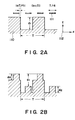
- FIG. 110 Denoted in the drawings at 110 is a glass substrate on which a diffraction grating of two-level structure has been formed.
- Denoted at 111 is a mask for use in second exposure.
- one period of the two-level structure is T
- the mask 111 has a light blocking portion of a width T/4.
- Denoted at 112 is a coordinate axis for explanation, and the pattern formed on the glass substrate 110 has a periodicity in X-axis direction.
- Figure 1A shows a state in which the mask 111 is deviated from an ideal position, in the positive X-axis direction by aT/4 (a>0).
- a finished diffractive optical element will have a shape such as shown in Figure 1B.
- Figure 2A shows a state in which the mask 111 is deviated from an ideal position, in the negative X-axis direction by
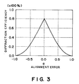
- Equation (1) is derived in accordance with scalar theory, and details of it will be described later with reference to embodiments of the present invention. The result can be shown in a graph, such as that of Figure 3.
- a 0
- an ideal diffraction efficiency of 81% is attainable with respect to the four-level structure.
- the diffraction efficiency decreases considerably. Since the decrease of diffraction efficiency leads to various problems such as a decrease of usable light quantity or an increase of unnecessary diffraction light, causing flare or the like, it should be suppressed as much as possible.
- an optical element manufacturing method comprising: a first process for forming a mask pattern on a substrate; and a second process for forming a step-like structure on the substrate by use of the mask pattern; wherein the first and second processes are repeated N times, and wherein, before execution of the (k)th time second process where 2 ⁇ k ⁇ N, there is a process for determining a relative alignment error between a mask pattern as formed through the (k)th time first process and a mask pattern as formed through the (k-1)th time first process; and wherein the height of the step-like structure to be defined by the (k)th time second process is determined in accordance with the alignment error.
- an optical element manufacturing method comprising: a first process for forming a first mask pattern on a substrate; a second process for forming a step-like structure on the substrate by use of the first mask pattern; a third process for forming a second mask pattern on the substrate; a fourth process for determining a relative alignment error between the first and second mask patterns; and a fifth process for forming a step-like structure on the substrate by use of the second mask pattern, wherein the height of the step-like structure to be formed through the fifth process is determined in accordance with the alignment error.
- an optical element manufacturing method comprising: a first process for forming a mask pattern on a substrate; a second process for determining a relative alignment error between a mask pattern just having been formed and a mask pattern previously formed; and a third process for forming a step-like structure on the substrate by use of the mask pattern just having been formed, wherein the height of the step-like structure to be formed through the third process is determined in accordance with the alignment error.
- the present invention can be applied to an optical element manufacturing system, or to an illumination system or exposure apparatus having an optical element manufactured in accordance with the optical element manufacturing method. Also, the invention can be applied to a device manufacturing method which uses such an exposure apparatus.
- Figures 1A and 1B are schematic views, respectively, for explaining the relation between alignment error and the shape of optical element.
- Figures 2A and 2B are schematic views, respectively, for explaining another example of the relation between alignment error and the shape of optical element.
- Figure 3 is a graph for explaining the relationship between alignment error and diffraction efficiency.
- Figure 4 is a flow chart for explaining the procedure of manufacture of a binary type diffractive optical element according to an embodiment of the present invention.
- Figure 5 is aseries of schematic views for explaining the procedure of manufacture of a binary type diffractive optical element of four-level structure, according to an embodiment of the present invention.
- Figure 6 is a schematic view for explaining the relation between alignment error and phase distribution of optical element.
- Figure 7 is a schematic view for explaining another example of the relation between alignment error and phase distribution of optical element.
- Figure 8 is a graph for explaining the relationship between the depth of second etching and diffraction efficiency.
- Figures 9A and 9B are schematic views, respectively, for explaining examples of mask pattern.
- Figure 10 is a schematic view for explaining positional relationship between images of two alignment error measurement marks.
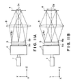
- Figures 11A and 11B are schematic views, respectively, of a main portion of an illumination system into which an optical element manufactured in accordance with an embodiment of the present invention is incorporated.
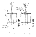
- Figures 12A and 12B are enlarged and schematic views, respectively, of a diffractive optical element in the structure shown in Figures 11A and 11B.
- Figure 13 is a schematic view of a main portion of a projection exposure apparatus into which an optical element manufactured in accordance with an embodiment of the present invention is incorporated.
- Figure 14 is a flow chart for explaining device manufacturing processes.
- Figure 15 is a flow chart for explaining details of a wafer process in the procedure of Figure 14.
- Figure 16 is a schematic view of a manufacturing system based on a manufacturing method according to an embodiment of the present invention.
- Figure 4 is a flow chart of optical element manufacturing method, according to an embodiment of the present invention.
- Figure 5 is a schematic view for explaining the procedure of manufacture of an optical element in this embodiment of the present invention, for manufacturing a binary type diffractive optical element of four-level (four-step) structure.
- each of the resists 101 and 104 comprises a positive type resist.
- Denoted at 102 is a mask (first mask) to be used for a first exposure
- denoted at 105 is a mask (second mask) to be used for a second exposure.
- Denoted at 103 or 106 is exposure light.
- process A a pattern of the first mask 102 is transferred to the resist 101 by use of the exposure light 103.
- process B development of the resist 101 is performed.
- process C etching of the glass substrate.100 is performed while the resist pattern defined by the development is used as a mask pattern.
- process D unnecessary resist on the substrate 100 is removed, whereby a binary type optical element of two-level step structure is accomplished.
- a resist material (104) is applied again, and in process E the second mask 105 is used to perform a second exposure.
- the pattern of the mask 105 has a pitch a half of the pattern of the mask 102.
- the exposure is performed while correctly aligning the edge of a light blocking portion of the mask pattern with the edge of the two-level binary structure.
- process F development treatment is performed whereby a resist pattern as illustrated is formed.
- Process E has been explained above with respect to an example wherein the pattern of the mask 105 and the pattern of the mask 102 are correctly aligned with each other. Practically, however, it is not easy to align the mask 105 with the mask 102, more exactly, to align the mask 105 with the substrate 100 on which a two-level step-like structure has been formed by use of the mask 102. In practice, there occurs a registration error (alignment error) between these masks.
- process H unnecessary resist is removed whereby a binary type diffractive optical element of four-level structure is accomplished.
- the relation between the alignment error of the second mask 105 and the diffraction efficiency of first-order diffraction light is such as shown in Figure 3.
- calculation of diffraction efficiency is performed again, while taking into account the relation with the etching depth in the second etching process.
- the diffraction efficiency of (m)th-order diffraction light from a structure which has a period T in X direction and which provides a phase distribution p(x) with respect to incident plane wave front can be calculated by using a square of an absolute value of that is, by using
- the shape shown in Figure 1B where a>0 may be expressed in terms of a phase function.
- phase function p(x) may be determined as illustrated in Figure 6. While the origin of phase may be set as desired, here, for convenience, it is set as shown in Figure 6. Calculation may be made while taking the X-direction range from 0 to T as one period and, in regard to first-order diffraction light, from equation, the following equation may be derived.
- Figure 8 shows the result of calculation of diffraction efficiency of first-order diffraction light, while taking the parameter b, representing the second time etching depth d 2 , on the axis of abscissa.
- the magnitude of alignment error is measured and, in accordance with it, the etching depth d 2 of the second etching is controlled.
- the present invention enables manufacture of good diffractive optical elements.
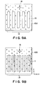
- Figures 9A and 9B are schematic views of a first mask 102 and a second mask 105, respectively. If a positive type resist is used, images of openings 10 and 11 will be transferred to a glass substrate. These masks are formed with pattern groups 12 and 13 to be used for forming a binary type diffractive optical element. Additionally, there are alignment error measurement marks 14 and 15, formed on the first and second masks 102 and 105, respectively.
- the pattern group 12, the alignment error measurement mark 14, the pattern group 13, and the alignment error measurement mark 15 are disposed in a predetermined positional relationship, such that, only when the pattern groups 12 and 13 are registered idealistically with each other upon the glass substrate, the images of the two alignment error measurement marks 14 and 15 are placed exactly at the same position.
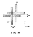
- Figure 10 shows an example of positional relation between an image 20 of the alignment error measurement mark 14 and an image 21 of the alignment error measurement mark 15, after completion of second exposure (process F).
- Figures 9A and 9B are equipped with alignment marks (not shown), and the positional relation between these masks is controlled by using these alignment marks. Practically, however, due to various factors, pattern transfer is performed with misalignment. Figure 10 shows an example with such misalignment.
- the positional relation between the images 20 and 21 of the two alignment error measurement marks 14 and 15 can be detected.
- the deviation between the images 20 and 21 may be resolved into x-component and y-component.
- x-component ( ⁇ x) corresponds to the alignment error which adversely affects the diffraction efficiency, in this example.
- an optimum etching depth d 2 in the second etching process (process G) is calculated in accordance with equation (5), and the second etching process is performed on the basis of this information.
- the present invention is similarly applicable to a binary diffractive optical element of the type having a two-dimensional period distribution and, additionally, having non-uniform period, such as a Fresnel lens, for example.
- a binary diffractive optical element of the type having a two-dimensional period distribution and, additionally, having non-uniform period, such as a Fresnel lens, for example.
- the alignment error for calculation of etching depth not only ⁇ x in Figure 10 but also ⁇ y may be used.
- Figures 11A and 11B are schematic views of a main portion of an illumination system having a diffractive optical element, according to an embodiment of the present invention.
- Figure 11A is taken on a first plane, i.e., X-Z plane.
- Figure 11B is taken on a second plane, i.e., Y-Z plane.
- Denoted in the drawings at 1 is a light source such as a Hg lamp or excimer laser, for example.
- Denoted at 2 is a beam shaping optical system including a beam compressor, for example. It serves to adjust the light from the light source 1 into a desired beam shape, and to project the same on the light entrance surface 5a of an optical integrator 5 which serves as a homogenizer.
- the optical integrator 5 has two diffractive optical elements, that is, first and second diffractive optical elements having different refractive powers with respect to both of X-Z sectional plane ( Figure 11A) and Y-Z sectional plane ( Figure 11B).
- a plurality of secondary light sources are defined at the light exit surface 5b thereof.
- Denoted at 3 is a condenser lens for collecting light beams from the secondary light sources, at the light exit surface of the optical integrator 5, so that they are superposed one upon another on the surface 4 to be illuminated.
- the light emitted by the light source 1 is transformed by the beam shaping optical system 2 into a desired beam diameter, and then it is projected on the light entrance surface 5a of the optical integrator 5.
- a plurality of secondary light sources are defined at the light exit surface 5b. The lights from these secondary light sources at the light exit surface 5b are then projected by the condenser lens 3 to Koehler-illuminate the surface 4 to be illuminated.
- the optical integrator 5 is arranged to have a numerical aperture ⁇ x with respect to X-direction sectional plane of Figure 11A and a numerical aperture ⁇ y with respect to Y-direction sectional plane of Figure 11B, which are different from each other, such that the illumination regions along these sectional planes have different widths Dx and Dy.
- Figures 12A and 12B are schematic views of a main portion of the optical integrator 5, shown in Figures 11A and 11B.
- Figure 12A is taken on X-Z plane
- Figure 12B is taken on Y-Z plane.
- the optical integrator 5 comprises a number of small diffractive optical elements 21 with focal length f ix , having a power in X-direction sectional plane as viewed in the drawing and being arrayed at the front side (light source 1 side) of the same substrate 20. Also, the optical integrator further comprises a number of small diffractive optical element 22 with focal length f iy , having a power in Y-direction sectional plane as viewed in the drawing and being arrayed at the back side of the substrate.
- the combinations of these small diffractive optical elements 21 and 22 provide a first diffractive optical element and a second diffractive optical element, respectively.
- the focal lengths f ix and f iy they are in a relation f ix > f iy and both of them have a positive value.
- the refractive powers of the first and second diffractive optical elements 21 and 22 as well as the thickness of the substrate 20 and the refractivity of the material thereof, for example, are selected and adjusted so that the focal point position of the light passing through the first and second diffractive optical elements 21 and 22 is in exact registration, with respect to the first and second planes. With this arrangement, an illumination region of predetermined shape can be defined efficiently.
- Small diffractive optical element of this embodiment can be manufactured by use of optical lithography technique as described.
- an element lens smaller than an element lens as attainable with conventional polishing process, for example can be manufactured easily. This makes it possible to increase the number of element lenses considerably and consequently to increase the number of secondary light sources considerably. Thus, illumination of higher uniformity can be realized.
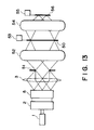
- Figure 13 is a schematic view of a main portion of a projection exposure apparatus having a diffractive optical element, according to an embodiment of the present invention.
- Denoted in the drawing at 1 is a light source, and denoted at 2 is a beam shaping optical system.
- Denoted at 5 is an optical integrator, and denoted at 3 is a condenser lens. These components are similar to those used in the illumination system of Figures 11A and 11B.
- Denoted at 51 is a stop, which corresponds to the position of the surface 4 to be illuminated ( Figure 11A or 11B).
- Denoted at 52 is a stop imaging lens for projecting an image of the aperture shape of the stop 51 on to a reticle 50 which is disposed on the surface to be illuminated.
- the illumination region on the reticle 50 surface has a shape analogous to the aperture shape of the stop 51.
- Denoted at 54 is a projection lens (projection optical system) for projecting a pattern on the reticle 50 surface on to the surface of a photosensitive substrate (wafer) 56.
- Denoted at 53 is driving means for moving the reticle 50
- denoted at 55 is driving means for moving the wafer 56.
- a circuit pattern of the reticle 50 is printed, by projection through the projection lens 54, on the wafer 56 being coated with a photosensitive material such as a resist, in step-and-scan procedure.
- the pattern of the reticle 50 is not illuminated at once. Rather, the illumination area is defined in a slit-like shape, for example. Thus, a pattern of the reticle 50 placed within such illumination area is projected and transferred by the projection lens 54 to the exposure area on the wafer 56.
- the reticle 56 is placed on a reticle stage, and it can be scanningly moved in X direction, for example, by the driving means 53.
- the wafer 56 is placed on a movable stage which can be scanningly moved by the driving means 55, along the X-axis direction and in an opposite direction to the reticle 50 movement. More specifically, the reticle 50 and the wafer 56 are scanningly moved in opposite directions, in synchronism with each other, at a speed ratio corresponding to the projection magnification of the projection lens 54.
- a diffractive optical element is used in an illumination system
- a diffractive optical element of ring-like shape manufactured in accordance with the present invention may be used in a projection optical system.
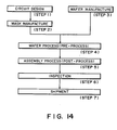
- Figure 14 is a flow chart of procedure for manufacture of microdevices such as semiconductor chips (e.g. ICs or LSIs), liquid crystal panels, or CCDs, for example.
- semiconductor chips e.g. ICs or LSIs
- liquid crystal panels e.g. LCDs
- CCDs complementary metal-oxide-semiconductors
- Step 1 is a design process for designing a circuit of a semiconductor device.
- Step 2 is a process for making a mask on the basis of the circuit pattern design.
- Step 3 is a process for preparing a wafer by using a material such as silicon.
- Step 4 is a wafer process which is called a pre-process wherein, by using the so prepared mask and wafer, circuits are practically formed on the wafer through lithography.
- Step 5 subsequent to this is an assembling step which is called a post-process wherein the wafer having been processed by step 4 is formed into semiconductor chips.
- This step includes assembling (dicing and bonding) process and packaging (chip sealing) process.
- Step 6 is an inspection step wherein operation check, durability check and so on for the semiconductor devices provided by step 5, are carried out. With these processes, semiconductor devices are completed and they are shipped (step 7).
- Step 15 is a flow chart showing details of the wafer process.
- Step 11 is an oxidation process for oxidizing the surface of a wafer.
- Step 12 is a CVD process for forming an insulating film on the wafer surface.
- Step 13 is an electrode forming process for forming electrodes upon the wafer by vapor deposition.
- Step 14 is an ion implanting process for implanting ions to the wafer.
- Step 15 is a resist process for applying a resist (photosensitive material) to the wafer.
- Step 16 is an exposure process for printing, by exposure, the circuit pattern of the mask on the wafer through the exposure apparatus described above.
- Step 17 is a developing process for developing the exposed wafer.
- Step 18 is an etching process for removing portions other than the developed resist image.
- Step 19 is a resist separation process for separating the resist material remaining on the wafer after being subjected to the etching process. By repeating these processes, circuit patterns are superposedly formed on the wafer.
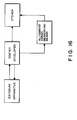
- denoted at 201 is an exposure apparatus for performing an exposure process.
- Denoted at 202 is a coater and developer, for performing resist coating and resist development after exposure.
- Denoted at 203 is an etcher for performing the etching process while using a developed resist pattern as a mask pattern.
- Denoted at 204 is alignment error measuring means for measuring, after second time resist pattern development, alignment error between a mask having been used previously and a mask just to be used or just having been used.
- the optical element manufacturing method such as described with reference to Figure 4 or 5, for example, can be embodied in this manufacturing system, for example.
Abstract
Description


Practically, however, due to various factors, pattern transfer is performed with misalignment. Figure 10 shows an example with such misalignment.
Claims (17)
- An optical element manufacturing method, comprising:a first process for forming a mask pattern on a substrate; anda second process for forming a step-like structure on the substrate by use of the mask pattern;wherein the first and second processes are repeated N times, and wherein, before execution of the (k)th time second process where 2≦k≦N, there is a process for determining a relative alignment error between a mask pattern as formed through the (k)th time first process and a mask pattern as formed through the (k-1)th time first process; andwherein the height of the step-like structure to be defined by the (k)th time second process is determined in accordance with the alignment error.
- A method according to Claim 1, wherein the first and second processes are repeated by N times, by which a step-like structure with 2N levels is formed on the substrate.
- A method according to Claim 1, wherein the mask pattern comprises a resist having been developed.
- A method according to Claim 3, wherein the first process includes a sub-process for coating the substrate with a resist, a sub-process for lithographically transferring a pattern on to the resist and a sub-process for developing the pattern transferred to the resist.
- A method according to Claim 3, wherein the second process includes a sub-process for etching the substrate, wherein the height of the step-like structure as determined in accordance with the alignment error corresponds to the depth of the etching, and a sub-process for removing a resist from the substrate.
- An optical element manufacturing method, comprising:a first process for forming a first mask pattern on a substrate;a second process for forming a step-like structure on the substrate by use of the first mask pattern;a third process for forming a second mask pattern on the substrate;a fourth process for determining a relative alignment error between the first and second mask patterns; anda fifth process for forming a step-like structure on the substrate by use of the second mask pattern, wherein the height of the step-like structure to be formed through the fifth process is determined in accordance with the alignment error.
- An optical element manufacturing method, comprising:a first process for forming a mask pattern on a substrate;a second process for determining a relative alignment error between a mask pattern just having been formed and a mask pattern previously formed; anda third process for forming a step-like structure on the substrate by use of the mask pattern just having been formed, wherein the height of the step-like structure to be formed through the third process is determined in accordance with the alignment error.
- An optical element manufacturing system, comprising:means for forming a mask pattern on a substrate;means for determining a relative alignment error between a mask pattern just having been formed and a mask pattern previously formed; andmeans for forming a step-like structure on the substrate by use of the mask pattern just having been formed, wherein the height of the step-like structure to be formed through said step-like structure forming means is determined in accordance with the alignment error.
- An illumination system, comprising:
light directing means for directing illumination light supplied from a light source to an object to be illuminated, said light directing means including an optical element having been manufactured through a procedure which includes a first process for forming a mask pattern on a substrate, and a second process for forming a step-like structure on the substrate by use of the mask pattern, wherein the first and second processes are repeated N times, and wherein, before execution of the (k)th time second process where 2≦k≦N, there is a process for determining a relative alignment error between a mask pattern as formed through the (k)th time first process and a mask pattern as formed through the (k-1)th time first process, and wherein the height of the step-like structure to be defined by the (k)th time second process is determined in accordance with the alignment error. - An illumination system, comprising:
light directing means for directing illumination light supplied from a light source to an object to be illuminated, said light directing means including an optical element having been manufactured through a procedure which includes a first process for forming a first mask pattern on a substrate, a second process for forming a step-like structure on the substrate by use of the first mask pattern, a third process for forming a second mask pattern on the substrate, a fourth process for determining a relative alignment error between the first and second mask patterns, and a fifth process for forming a step-like structure on the substrate by use of the second mask pattern, wherein the height of the step-like structure to be formed through the fifth process is determined in accordance with the alignment error. - An illumination system, comprising:
light directing means for directing illumination light supplied from a light source to an object to be illuminated, said light directing means including an optical element having been manufactured through a procedure which includes a first process for forming a mask pattern on a substrate, a second process for determining a relative alignment error between a mask pattern just having been formed and a mask pattern previously formed, and a third process for forming a step-like structure on the substrate by use of the mask pattern just having been formed, wherein the height of the step-like structure to be formed through the third process is determined in accordance with the alignment error. - An exposure apparatus, comprising:illumination means for directing illumination light supplied from a light source to a reticle; andprojection means for projecting an image of the reticle on to a wafer;
wherein at least one of said illumination means and said projection means includes an optical element having been manufactured through a procedure which includes a first process for forming a mask pattern on a substrate, and a second process for forming a step-like structure on the substrate by use of the mask pattern, wherein the first and second processes are repeated N times, and wherein, before execution of the (k)th time second process where 2≦k≦N, there is a process for determining a relative alignment error between a mask pattern as formed through the (k)th time first process and a mask pattern as formed through the (k-1)th time first process, and wherein the height of the step-like structure to be defined by the (k)th time second process is determined in accordance with the alignment error. - An exposure apparatus, comprising:illumination means for directing illumination light supplied from a light source to a reticle; andprojection means for projecting an image of the reticle on to a wafer;wherein at least one of said illumination means and said projection means includes an optical element having been manufactured through a procedure which includes a first process for forming a first mask pattern on a substrate, a second process for forming a step-like structure on the substrate by use of the first mask pattern, a third process for forming a second mask pattern on the substrate, a fourth process for determining a relative alignment error between the first and second mask patterns, and a fifth process for forming a step-like structure on the substrate by use of the second mask pattern, wherein the height of the step-like structure to be formed through the fifth process is determined in accordance with the alignment error.
- An exposure apparatus, comprising:illumination means for directing illumination light supplied from a light source to a reticle; andprojection means for projecting an image of the reticle on to a wafer;wherein at least one of said illumination means and said projection means includes an optical element having been manufactured through a procedure which includes a first process for forming a mask pattern on a substrate, a second process for determining a relative alignment error between a mask pattern just having been formed and a mask pattern previously formed, and a third process for forming a step-like structure on the substrate by use of the mask pattern just having been formed, wherein the height of the step-like structure to be formed through the third process is determined in accordance with the alignment error.
- A device manufacturing method, comprising the steps of:transferring an image of a reticle on to a wafer by exposure, with use of an exposure apparatus as recited in any of claims 12 to 14; anddeveloping the wafer.
- A process for manufacturing a device, including the steps of:transferring an image of a reticle on to a wafer by exposure; andsubsequently using the exposed wafer to manufacture the device, wherein the transfer of the image to the wafer is achieved by means of an exposure apparatus as set forth in any of claims 12 to 14.
- A device manufactured by the method of claim 15 or claim 16.
Applications Claiming Priority (3)
| Application Number | Priority Date | Filing Date | Title |
|---|---|---|---|
| JP281830/96 | 1996-10-03 | ||
| JP28183096A JP3287236B2 (en) | 1996-10-03 | 1996-10-03 | Manufacturing method of diffractive optical element |
| JP28183096 | 1996-10-03 |
Publications (3)
| Publication Number | Publication Date |
|---|---|
| EP0834751A2 true EP0834751A2 (en) | 1998-04-08 |
| EP0834751A3 EP0834751A3 (en) | 1999-04-14 |
| EP0834751B1 EP0834751B1 (en) | 2002-07-31 |
Family
ID=17644608
Family Applications (1)
| Application Number | Title | Priority Date | Filing Date |
|---|---|---|---|
| EP97307810A Expired - Lifetime EP0834751B1 (en) | 1996-10-03 | 1997-10-02 | Optical element manufacturing method |
Country Status (4)
| Country | Link |
|---|---|
| US (2) | US6120950A (en) |
| EP (1) | EP0834751B1 (en) |
| JP (1) | JP3287236B2 (en) |
| DE (1) | DE69714368T2 (en) |
Cited By (4)
| Publication number | Priority date | Publication date | Assignee | Title |
|---|---|---|---|---|
| EP1081551A2 (en) * | 1999-09-03 | 2001-03-07 | Canon Kabushiki Kaisha | Two-dimensional phase element and method of manufacturing the same |
| EP1022589B1 (en) * | 1999-01-19 | 2005-07-27 | Canon Kabushiki Kaisha | Diffractive optical element |
| FR2981460A1 (en) * | 2011-10-18 | 2013-04-19 | Commissariat Energie Atomique | METHOD FOR PRODUCING A REFRACTIVE OR DIFFRACTIVE OPTICAL DEVICE |
| EP3333884A1 (en) * | 2000-09-19 | 2018-06-13 | Nova Measuring Instruments Limited | Lateral shift measurement using an optical technique |
Families Citing this family (26)
| Publication number | Priority date | Publication date | Assignee | Title |
|---|---|---|---|---|
| JP3287236B2 (en) * | 1996-10-03 | 2002-06-04 | キヤノン株式会社 | Manufacturing method of diffractive optical element |
| AU2300099A (en) * | 1998-02-09 | 1999-08-23 | Nikon Corporation | Method of adjusting position detector |
| JP2000098116A (en) * | 1998-09-18 | 2000-04-07 | Canon Inc | Element or manufacture of mold for manufacturing element |
| JP3359309B2 (en) * | 1998-10-29 | 2002-12-24 | キヤノン株式会社 | Method for manufacturing binary diffractive optical element |
| US6856392B1 (en) * | 1998-11-09 | 2005-02-15 | Canon Kabushiki Kaisha | Optical element with alignment mark, and optical system having such optical element |
| JP2001174615A (en) * | 1999-04-15 | 2001-06-29 | Nikon Corp | Diffraction optical element, method of producing the element, illumination device equipped with the element, projection exposure device, exposure method, light homogenizer, and method of producing the light homogenizer |
| US6476908B1 (en) * | 2000-04-10 | 2002-11-05 | Eclipse Optics, Inc. | Optical probe |
| WO2001084382A1 (en) * | 2000-05-04 | 2001-11-08 | Kla-Tencor, Inc. | Methods and systems for lithography process control |
| EP2506089A3 (en) * | 2000-05-30 | 2012-12-19 | Dai Nippon Printing Co., Ltd. | Computer-generated hologram and its fabrication process, reflector using a computer-generated hologram, and reflective liquid crystal display |
| US6891627B1 (en) | 2000-09-20 | 2005-05-10 | Kla-Tencor Technologies Corp. | Methods and systems for determining a critical dimension and overlay of a specimen |
| US20030002043A1 (en) | 2001-04-10 | 2003-01-02 | Kla-Tencor Corporation | Periodic patterns and technique to control misalignment |
| JP3970106B2 (en) * | 2001-05-23 | 2007-09-05 | エーエスエムエル ネザーランズ ビー.ブイ. | Substrate comprising alignment marks in a substantially transparent process layer, a mask for exposing the marks, and a device manufacturing method |
| US6614517B1 (en) * | 2001-09-18 | 2003-09-02 | Nayna Networks, Inc. | Method and computer aided apparatus for aligning large density fiber arrays |
| US6905618B2 (en) * | 2002-07-30 | 2005-06-14 | Agilent Technologies, Inc. | Diffractive optical elements and methods of making the same |
| EP1498779A3 (en) * | 2003-07-11 | 2005-03-23 | ASML Netherlands B.V. | Marker structure for alignment or overlay |
| SG108975A1 (en) * | 2003-07-11 | 2005-02-28 | Asml Netherlands Bv | Marker structure for alignment or overlay to correct pattern induced displacement, mask pattern for defining such a marker structure and lithographic projection apparatus using such a mask pattern |
| JP4345625B2 (en) * | 2004-09-22 | 2009-10-14 | 株式会社島津製作所 | Diffraction grating |
| JP5048930B2 (en) * | 2005-06-08 | 2012-10-17 | ラピスセミコンダクタ株式会社 | Diffractive optical element and method of manufacturing diffractive optical element |
| CN1313404C (en) * | 2005-08-24 | 2007-05-02 | 中国科学院上海光学精密机械研究所 | Preparation method of low refractivity glass doped with erbium, fluorine and phosphor |
| WO2008086827A1 (en) * | 2007-01-16 | 2008-07-24 | Carl Zeiss Smt Ag | Projection exposure method and projection exposure system therefor |
| CN101785107B (en) * | 2007-06-13 | 2012-07-04 | 楷能洁有限公司 | Method for marking wafers |
| NL1036877A (en) * | 2008-08-18 | 2010-03-09 | Asml Netherlands Bv | Diffractive optical element, lithographic apparatus and semiconductor device manufacturing method. |
| JP5621201B2 (en) * | 2008-11-13 | 2014-11-12 | 凸版印刷株式会社 | Imprint mold manufacturing method and imprint mold |
| US20140030895A1 (en) | 2012-07-30 | 2014-01-30 | University Of Utah Research Foundation | Methods and system for generating a three-dimensional holographic mask |
| KR101635138B1 (en) * | 2014-09-05 | 2016-06-30 | 한국기계연구원 | Method of fabricating a multi-layered complex stamp and method of fabricating an anti-counterfeiting film using the multi-layered complex stamp |
| CN110113980B (en) | 2016-12-22 | 2022-04-05 | 奇跃公司 | Method and system for manufacturing shaped optical fiber elements for scanning fiber optic displays |
Family Cites Families (11)
| Publication number | Priority date | Publication date | Assignee | Title |
|---|---|---|---|---|
| DE3118802A1 (en) * | 1980-05-14 | 1982-02-25 | Canon K.K., Tokyo | PRESSURE TRANSFER DEVICE |
| NL8502624A (en) * | 1985-09-26 | 1987-04-16 | Philips Nv | METHOD FOR DETERMINING THE EXPOSURE DOSE OF A PHOTOSENSITIVE COATING LAYER. |
| US5161059A (en) * | 1987-09-21 | 1992-11-03 | Massachusetts Institute Of Technology | High-efficiency, multilevel, diffractive optical elements |
| US4895790A (en) * | 1987-09-21 | 1990-01-23 | Massachusetts Institute Of Technology | High-efficiency, multilevel, diffractive optical elements |
| US5156943A (en) * | 1987-10-25 | 1992-10-20 | Whitney Theodore R | High resolution imagery systems and methods |
| JP2796196B2 (en) * | 1990-04-12 | 1998-09-10 | 松下電器産業株式会社 | Optical head device |
| US5503959A (en) * | 1991-10-31 | 1996-04-02 | Intel Corporation | Lithographic technique for patterning a semiconductor device |
| US5631762A (en) * | 1993-06-04 | 1997-05-20 | Hitachi Koki Co., Ltd. | Multi-beam generating element and optical printing apparatus therewith |
| US5468324A (en) * | 1994-03-08 | 1995-11-21 | Hong; Gilbert H. | Spin-on and peel polymer film method of data recording duplication and micro-structure fabrication |
| US5995285A (en) | 1996-07-09 | 1999-11-30 | Canon Kabushiki Kaisha | Multilevel optical diffraction device with antireflection film and exposure apparatus |
| JP3287236B2 (en) * | 1996-10-03 | 2002-06-04 | キヤノン株式会社 | Manufacturing method of diffractive optical element |
-
1996
- 1996-10-03 JP JP28183096A patent/JP3287236B2/en not_active Expired - Fee Related
-
1997
- 1997-10-02 DE DE69714368T patent/DE69714368T2/en not_active Expired - Fee Related
- 1997-10-02 EP EP97307810A patent/EP0834751B1/en not_active Expired - Lifetime
- 1997-10-02 US US08/942,979 patent/US6120950A/en not_active Expired - Lifetime
-
2000
- 2000-03-03 US US09/518,103 patent/US6301001B1/en not_active Expired - Lifetime
Non-Patent Citations (3)
| Title |
|---|
| O'SHEA D C ET AL: "GRAY-SCALE MASKS FOR DIFFRACTIVE-OPTICS FABRICATION: II. SPATIALLY FILTERED HALFTONE SCREENS" APPLIED OPTICS, vol. 34, no. 32, 10 November 1995, pages 7518-7526, XP000537265 * |
| STERN M B ET AL: "FABRICATING BINARY OPTICS: PROCESS VARIABLES CRITICAL TO OPTICAL EFFICIENCY" JOURNAL OF VACUUM SCIENCE AND TECHNOLOGY: PART B, vol. 9, no. 6, 1 November 1991, pages 3117-3121, XP000268528 * |
| SULESKI T J ET AL: "GRAY-SCALE MASKS FOR DIFFRACTIVE-OPTICS FABRICATION: 1. COMMERCIAL SLIDE IMAGERS" APPLIED OPTICS, vol. 34, no. 32, 10 November 1995, pages 7507-7517, XP000537264 * |
Cited By (8)
| Publication number | Priority date | Publication date | Assignee | Title |
|---|---|---|---|---|
| EP1022589B1 (en) * | 1999-01-19 | 2005-07-27 | Canon Kabushiki Kaisha | Diffractive optical element |
| EP1081551A2 (en) * | 1999-09-03 | 2001-03-07 | Canon Kabushiki Kaisha | Two-dimensional phase element and method of manufacturing the same |
| EP1081551A3 (en) * | 1999-09-03 | 2005-02-09 | Canon Kabushiki Kaisha | Two-dimensional phase element and method of manufacturing the same |
| EP3333884A1 (en) * | 2000-09-19 | 2018-06-13 | Nova Measuring Instruments Limited | Lateral shift measurement using an optical technique |
| EP1410435B1 (en) * | 2000-09-19 | 2019-11-06 | Nova Measuring Instruments Limited | Lateral shift measurement using an optical technique |
| FR2981460A1 (en) * | 2011-10-18 | 2013-04-19 | Commissariat Energie Atomique | METHOD FOR PRODUCING A REFRACTIVE OR DIFFRACTIVE OPTICAL DEVICE |
| WO2013057152A1 (en) * | 2011-10-18 | 2013-04-25 | Commissariat A L'energie Atomique Et Aux Energies Alternatives | Method for producing a refractive or diffractive optical device |
| US9529127B2 (en) | 2011-10-18 | 2016-12-27 | Commissariat A L'energie Atomique Et Aux Energies Alternatives | Method for producing a refractive or diffractive optical device |
Also Published As
| Publication number | Publication date |
|---|---|
| JP3287236B2 (en) | 2002-06-04 |
| JPH10111407A (en) | 1998-04-28 |
| EP0834751B1 (en) | 2002-07-31 |
| US6120950A (en) | 2000-09-19 |
| DE69714368T2 (en) | 2003-03-06 |
| US6301001B1 (en) | 2001-10-09 |
| EP0834751A3 (en) | 1999-04-14 |
| DE69714368D1 (en) | 2002-09-05 |
Similar Documents
| Publication | Publication Date | Title |
|---|---|---|
| EP0834751B1 (en) | Optical element manufacturing method | |
| US6633390B2 (en) | Focus measurement in projection exposure apparatus | |
| US6930754B1 (en) | Multiple exposure method | |
| US7079220B2 (en) | Illumination optical system and method, and exposure apparatus | |
| US6333777B1 (en) | Exposure apparatus and device manufacturing method | |
| JP5500454B2 (en) | Optical integrator, illumination optical apparatus, exposure apparatus, exposure method, and device manufacturing method | |
| US6008942A (en) | Diffractive optical element and optical instrument having the same | |
| EP0952491A2 (en) | Lithography apparatus | |
| KR20020090134A (en) | Substrate provided with an Alignment Mark, Method of Designing a Mask, Computer Program, Mask for Exposing said Mark, Device Manufacturing Method, and Device Manufactured Thereby | |
| US6816234B2 (en) | Illumination optical system in exposure apparatus | |
| US5926257A (en) | Illumination optical system and exposure apparatus having the same | |
| US20060056038A1 (en) | Aberration correcting optical system | |
| EP1022589B1 (en) | Diffractive optical element | |
| US6731431B2 (en) | Optical unit having plural optical elements | |
| US6560044B2 (en) | Illumination optical system in exposure apparatus | |
| EP0811865B1 (en) | Illumination system and exposure apparatus | |
| US6377337B1 (en) | Projection exposure apparatus | |
| US6285440B1 (en) | Illumination system and projection exposure apparatus using the same | |
| US20040022068A1 (en) | Illumination optical system, exposure method and apparatus using the same | |
| US5495336A (en) | Position detecting method for detecting a positional relationship between a first object and a second object | |
| US5706077A (en) | Scan type projection exposure apparatus and microdevice manufacturing method using the same | |
| KR20030069070A (en) | Lithographic Apparatus, Alignment Method and Device Manufacturing Method | |
| JP2008124308A (en) | Exposure method and exposure apparatus, and device manufacturing method using the same | |
| JP3313932B2 (en) | Projection exposure equipment | |
| JPH1114813A (en) | Manufacture of diffraction optical element |
Legal Events
| Date | Code | Title | Description |
|---|---|---|---|
| PUAI | Public reference made under article 153(3) epc to a published international application that has entered the european phase |
Free format text: ORIGINAL CODE: 0009012 |
|
| AK | Designated contracting states |
Kind code of ref document: A2 Designated state(s): DE GB NL |
|
| PUAL | Search report despatched |
Free format text: ORIGINAL CODE: 0009013 |
|
| AK | Designated contracting states |
Kind code of ref document: A3 Designated state(s): AT BE CH DE DK ES FI FR GB GR IE IT LI LU MC NL PT SE |
|
| 17P | Request for examination filed |
Effective date: 19990830 |
|
| AKX | Designation fees paid |
Free format text: DE GB NL |
|
| 17Q | First examination report despatched |
Effective date: 20000315 |
|
| GRAG | Despatch of communication of intention to grant |
Free format text: ORIGINAL CODE: EPIDOS AGRA |
|
| GRAG | Despatch of communication of intention to grant |
Free format text: ORIGINAL CODE: EPIDOS AGRA |
|
| GRAH | Despatch of communication of intention to grant a patent |
Free format text: ORIGINAL CODE: EPIDOS IGRA |
|
| GRAH | Despatch of communication of intention to grant a patent |
Free format text: ORIGINAL CODE: EPIDOS IGRA |
|
| GRAA | (expected) grant |
Free format text: ORIGINAL CODE: 0009210 |
|
| AK | Designated contracting states |
Kind code of ref document: B1 Designated state(s): DE GB NL |
|
| REG | Reference to a national code |
Ref country code: GB Ref legal event code: FG4D |
|
| REF | Corresponds to: |
Ref document number: 69714368 Country of ref document: DE Date of ref document: 20020905 |
|
| PLBE | No opposition filed within time limit |
Free format text: ORIGINAL CODE: 0009261 |
|
| STAA | Information on the status of an ep patent application or granted ep patent |
Free format text: STATUS: NO OPPOSITION FILED WITHIN TIME LIMIT |
|
| 26N | No opposition filed |
Effective date: 20030506 |
|
| PGFP | Annual fee paid to national office [announced via postgrant information from national office to epo] |
Ref country code: NL Payment date: 20081017 Year of fee payment: 12 |
|
| PGFP | Annual fee paid to national office [announced via postgrant information from national office to epo] |
Ref country code: DE Payment date: 20081031 Year of fee payment: 12 |
|
| PGFP | Annual fee paid to national office [announced via postgrant information from national office to epo] |
Ref country code: GB Payment date: 20081029 Year of fee payment: 12 |
|
| REG | Reference to a national code |
Ref country code: NL Ref legal event code: V1 Effective date: 20100501 |
|
| PG25 | Lapsed in a contracting state [announced via postgrant information from national office to epo] |
Ref country code: NL Free format text: LAPSE BECAUSE OF NON-PAYMENT OF DUE FEES Effective date: 20100501 Ref country code: DE Free format text: LAPSE BECAUSE OF NON-PAYMENT OF DUE FEES Effective date: 20100501 |
|
| PG25 | Lapsed in a contracting state [announced via postgrant information from national office to epo] |
Ref country code: GB Free format text: LAPSE BECAUSE OF NON-PAYMENT OF DUE FEES Effective date: 20091002 |