Technical Field
The present invention relates to apparatus and
methods of providing an electrically conductive path
across a joint or gap between two or more adjacent parts
in order to provide a continuous conductive path
therebetween.
Background of the Invention
It is often useful to provide a continuous
conductive path between adjacent parts which are
themselves electrically conductive but which are
separated by a non conductive joint or gap.
For example, it is important that electronic
components on an aircraft be shielded from the effects of
external electromagnetic fields and from the effects of
lightning strikes. External electromagnetic fields,
referred to as EMI effects, can disrupt the operation of
on board electronic components by generating unwanted
voltage and current fluctuations in the wiring. These
fluctuations can also permanently damage the electronic
components.
During a lightning strike the electronic components
can be subjected to extremely high voltages and currents
which can seriously impair their operation as well as
result in permanent damage. In order to avoid this
problem, these components must be shielded from the
effects of the lightning strikes as well.
A common method of mitigating the potential damage
from EMI effects and lightning is to place a continuous
conductive shield around the electronic components which
are at risk. Often the outer surface or "skin" of the
aircraft is used as such a shield.
Often aircraft skins are made from composite
materials which are poor conductors and therefore are not
good shields against EMI effects and lightning . A
common solution to this problem is to add a metallic
conductive layer or wire mesh as part of the composite
skin panel to act as a conductor. Although this produces
a panel which is electrically conductive, it does not
solve the problem of providing for a continuous
conductive path between adjacent conductive panels.
Another reason for providing a continuous conductive
path between adjacent parts applies to the performance of
high frequency antennas. On some aircraft, the aircraft
skin is utilized as a high frequency antenna. In order
for this antenna to operate efficiently, conductive paths
between individual conductive panels of the aircraft skin
are necessary.
A number of approaches have been tried to achieve
conductivity between such composite panels.
For example, one suggested method has been to use
conductive fasteners to attach the panels to the
underlying frame of the aircraft so that a path of
conductivity is provided through the fasteners and frame
to the adjacent panels.
An additional problem related to the use of
composite materials is galvanic corrosion. This problem
arises when two dissimilar parts, such as a composite
skin and an aluminum frame, are joined together. A
solution to this problem has been to provide an
electrical insulator at the junction of these dissimilar
materials. This reduces the conductivity between the
dissimilar materials sufficiently so that the galvanic
corrosion is no longer a problem. However, the need to
protect such components from corrosion is sometimes
incompatible with the need for electrically conductivity
therebetween to obtain electromagnetic and/or lightning
shielding. More specifically, the use of insulators to
prevent galvanic corrosion eliminates the required
conductivity between panels that is essential to EMI and
lightning protection.
A number of other conventional EMI shields have been
disclosed. For example, U.S. Patent No. 5,250,342 by Lang
et al discloses a composite EMI shield having an embedded
aluminum wire mesh which is fabricated using nonporous
tape so that upon removal of the tape there are provided
clean conductive areas on either side of the shield for
conductive mating with adjoining parts using metal
straps, bolts or gaskets.
Other relevant patents include U.S. 5,127,601 and
U.S. 5,352,565, both by Schroeder, which disclose an
airplane lightning shield consisting of thin metallic
foil which is bonded to a composite surface using an
epoxy or adhesive.
In U.S. Patent No. 4,313,777 by Buckley et al there
is disclosed a one step method of inductively heating two
sheets of thermoplastic material and simultaneously
fixing electronic circuitry into the thermoplastic
material.
U.S. 3,431,348 by Watchung et al discloses a viewing
laminate containing an embedded wire screen which extends
beyond the periphery thereof to provide electrical
contact with an exterior conductor.
U.S. 5,473,111 by Hattori discloses an electronics
enclosure made of molded resin and having EMI shielding
which is molded integrally with the resin.
In U.S. 4,746,389 by DiGenova there is disclosed a
composite EMI shield having an embedded aluminum wire
mesh wherein the shield is fabricated using nonporous
tape so that when the tape is removed, there are exposed
clean conductive areas for providing a conductive path
with adjacent articles.
In U.S. 5,065,960 by Castellucci there is disclosed
a gap filler which is located between a gap formed
between adjacent metallic aircraft panels to improve
laminar flow and which is formed of an electrically
conductive material to prevent galvanic corrosion between
the panels.
U.S. 4,015,035 and U.S. 3,885,071, both by Blad et
al, disclose an apparatus and method of joining epoxy
composite articles whereby fibers of each of the
composite articles pass through and are intermeshed
across a joint bond line.
U.S. 5,370,921 by Cedarleaf discloses a composite
structure containing a conductive metallic wire screen or
foil layer.
U.S. 5,312,508 by Chisholm discloses a method for
attaching wire mesh heat sinks to electronic packages for
heat transfer purposes wherein the adhesive is displaced
from the areas between the wire mesh and the
semiconductor.
In U.S. 3,755,713 by Paszkowski, which is assigned
to the assignee of the present invention, there is
disclosed a method of applying wire mesh over a
fiberglass composite material to form an integral part of
the surface of the fiberglass in order to dissipate
airplane lightning strikes.
And U.S. 4,671,470 by Jonas discloses a method for
fastening aircraft wing spars and frame members to fiber
reinforced composite structures using H-shaped woven
strap connectors.
None of the above conventional methods are
satisfactory for achieving electrical conductivity across
a non conductive joint or gap between adjacent panels
while at the same time electrically isolating the
conductive panels from the underlying substructure in
order to prevent galvanic corrosion.
Summary of the Invention
In a first embodiment, the present invention
pertains to a conductive system including a first part
having an electrical conductor therein and a second part
which is separate from the first part and which has an
electrical conductor therein. The invention includes a
bridge for conducting electrical energy between the first
part and the second part. The bridge has an electrical
conductor therein which has a plurality of peaks. In
addition, this embodiment includes means for adhering the
bridge to the first part and the second part such that
the peaks of the bridge electrical conductor are in
contact with the electrical conductor of the first part
and the electrical conductor of the second part so as to
provide a conductive path between them.
In a second embodiment, the present invention
pertains to a method of providing a conductive path
between adjacent parts. This involves positioning a first
part adjacent to a second part such that there is a space
between the first part and the second part, and exposing
conductive portions of the first part and the second
part. Further steps include providing a conductive
workpiece having a plurality of peaks, and positioning
the conductive workpiece against the first part and the
second part such that the peaks of the conductive
workpiece are in contact with the exposed conductive
portions of the first part and the second part.
In addition, a liquid adhesive is applied to the
conductive workpiece and the first part and the second
part, and the conductive workpiece and the first part and
the second part are compressed together such that
excessive liquid adhesive between the conductive
workpiece and the first part and the second part is
caused to flow and escape through spaces beneath the
peaks of the conductive workpiece while the adhesive
cures.
There are a number of benefits of the present
invention. Although not totally inclusive, some of these
benefits include, providing an improved:
Brief Description of the Drawings
These and other objects and advantages of the
present invention will be described in further detail in
the following Detailed Description in conjunction with
the attaching drawings, in which:
Detailed Description
In an exemplary embodiment, the present invention
will be described for its use in providing an
electromagnetic shield for the V-22 Osprey aircraft.
However, it should be appreciated that the present
invention is not limited for use in aircraft or in any
particular aircraft type. Rather, the present invention
may be used in any situation where a conductive bridge is
needed between two adjacent conductive workpieces.
The V-22 Osprey is a fly-by-wire aircraft
constructed of graphite composite skin over a mostly
aluminum internal frame. It is a vertical take off and
landing airplane having as one of its missions the
transportation of shipboard marine personnel to and from
land. The combination of the graphite/aluminum
construction and the salt spray environment in which the
V-22 will be based necessitates exceptionally strict
corrosion protection measures. These measures inherently
isolate the conductive components of the aircraft.
In addition, the V-22 is an "all weather" weapons
system that must be able to survive a lightning strike
with minimal impact. This requires careful
electromagnetic shielding of the aircraft's fly-by-wire
flight control system. Furthermore, the V-22 must take
off vertically. Therefore, to minimize weight,
electromagnetic shielding using the aircraft's existing
structure must be accomplished whenever possible. This
requires electrical bonding between the conductive
structural components. However, most of the time these
components are required to be electrically isolated due
to corrosion considerations.
Before discussing the details of the present
invention, a short discussion of a conventional composite
skin panel will be provided. It has been found that
copper foil mesh embedded in epoxy resin provides the
optimum combination of direct effects protection and
indirect effects shielding while ensuring
maintainability, durability, and aerodynamic surface
smoothness, etc.
Most of the internal frames in the forward and
center sections of the V-22 aircraft are aluminum. A
representative aluminum frame member 12, shown in cross
section in FIG. 1, has attached thereto adjacent aircraft
graphite epoxy skin panels 14 which are separated by a
gap or joint 16. Due to the galvanic incompatibility of
aluminum and graphite, these materials must be
electrically isolated from each other in the event
electrolytes (such as salt water) are present. Sealants
and paint alone cannot sufficiently assure the exclusion
of electrolytes from within these structurally critical
joints. Therefore, it is necessary to use additional
means to electrically isolate the graphite epoxy skins 14
from the aluminum frames 12.
This is accomplished by incorporating a thin ply of
fiber glass 18 (FIG. 1) into the composite lay up on the
frame side of the skin panels. In addition, the entire
frame (including the side facing the graphite skin) is
anodized, primed and painted. Finally, the frames 12 are
attached to the skins 14 using K-coated titanium
fasteners 20. K-coat is an aluminum-pigmented coating
used on titanium fasteners to reduce galvanic corrosion
when installed in aluminum. This coating is non-conductive.
The electrical conductivity across skin panel joints
constructed in this manner is approximately 0.5 mhos per
meter of joint length. This is unacceptable for
electromagnetic shielding purposes.
The electromagnetic requirements which the V-22 skin
panel must satisfy are: (i) conductivity across each
panel joint of at least 200 mhos per meter (DC), (ii) the
ability to conduct zone 3 lightning current with a peak
of 200 kA divided by the local circumference of the
aircraft without causing damage sufficient to require
maintenance such that there is no impairment of the EMI
shielding effectiveness, and (iii) a 200 KA lightning
attachment to the joint must not cause loss of life or
aircraft, and (iv) any form of lightning damage to the
structure must be repairable at the "organization" level
of maintenance.
Other design requirements for the non conductive gap
or joint between adjacent skin panels include: (i)
incorporation of the corrosion protection features
outlined above, (ii) satisfying aerodynamic smoothness
and discontinuity requirements, (iii) being
manufacturable and repairable, (iv) withstanding maximum
structural static and vibration loads without degrading
electromagnetic shielding performance, and (v) keeping
cost and weight to a minimum.
In the typical graphite epoxy composite skin panel
used in the V-22 and indicated at 14 in FIG. 2, the
outermost layer of the composite lay-up is a thin copper
mesh having a density of about .049 pounds per square
foot. This mesh is pre-impregnated with a modified epoxy
supported adhesive film and cocured with the structural
graphite and resin matrix components. In an exemplary
embodiment, the adhesive film is FM-300 manufactured by
Cytec Industries located in Havre de Grace, Maryland.
The adhesive material is non-conductive and contains
a non-conductive fiber glass "scrim" mat. During the
cure cycle, the adhesive flows and envelops the copper
mesh, totally encasing it in adhesive. After cure, the
copper mesh is both physically and electrically isolated
from the outer (air-flow side) of the skin panel by the
cured adhesive as well as by the scrim mat. This is done
purposefully to protect the thin copper mesh from mild
impact damage and corrosion. This adhesive will partially
electrically isolate the copper mesh from the underlying
graphite.
Since the copper mesh is intended to provide
lightning protection, the ideal electrical "bridge"
between adjacent panels would provide a low resistance
path between the copper mesh present in adjacent skin
panels. Although electrical conduction between the
graphite layers would be electrically sufficient for EMI
shielding, such an electrical path may tend to see high
damage when stressed by lightning currents. Thus, there
is a preference for a copper mesh-to-copper mesh bridge
rather than a graphite-to-graphite bridge.
Having described a conventional aircraft skin panel,
attention now will be turned to the present invention. In
order to form a bridge indicated at 22 (FIGS. 1 and 2) of
the present invention, any non-conductive material which
is present, such as epoxy adhesive, is removed from the
surface of the air flow side of the skin panel 14. This
is done near joint 16 between adjacent panels 14a and 14b
in FIG. 2. In this manner, electromagnetic shielding
material 28 embedded in the skin 14 is exposed. In an
exemplary embodiment, the electromagnetic shielding
material 28 is a lightweight (.049 pounds per square
foot) thin expanded copper mesh which has been rolled and
flattened, and which is manufactured and sold under the
product name "AstroStrike Screening" by the Astroseal
Company of Old Saybrook, Connecticut.
The conductive portion of the bridge 22 uses a
heavier weight (.080 pounds per square foot) expanded
copper mesh which has not been rolled flat after
expansion. In an exemplary embodiment, the mesh 32 is
formed by stamping a thin (5 mil) foil of high purity
copper with a series of parallel overlapping slits. Once
this is accomplished, the foil is expanded in a
conventional manner by being pulled in opposite
directions which are perpendicular to the lengthwise axes
of the slits. The resultant pulling of the slits open
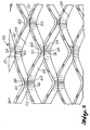
(expanding) forms a somewhat diamond shaped mesh 32 shown
in FIG. 3.
More specifically, the expanded mesh 32 includes
diamond shaped openings 34 which are formed by
perforating sheets of solid copper foil and then
expanding the copper foil. Each opening 34 appears to be
formed by two segments or "strands" of foil. These
include (i) a first segment having an upper left portion
36 extending from a bend 38 in an upward and rightward
direction (when viewing FIG. 3) where it joins with an
upper right portion 40 at a bend 42 wherein the upper
right portion 40 extends downward and rightward to a bend
44. The second segment of foil has a lower left portion
44 extending from a bend 46 in a downward and rightward
direction where it joins with a lower right portion 48 at
a bend 50 wherein the lower right portion 48 extends
upward and rightward to a bend 52.
In addition, each opening 34 is formed (i) at the
nine o'clock position by a bottom edge of segment bend 38
which is connected to a top edge of segment bend 46 along
a connection joint 53, and (ii) at the three o'clock
position by a bottom edge of segment bend 44 which is
connected to a top edge of segment bend 52 along a
connection joint 55. In addition, (i) at the twelve
o'clock position a top edge of segment bend 42 is
connected to a bottom edge of another segment bend 54
along a connection joint 57, and (ii) at the six o'clock
position a bottom edge of segment bend 50 is connected to
a top edge of another segment bend 56 along a connection
joint 59.
As shown in FIGS. 3 and 4, the individual segments
of foil mesh do not lie in the same plane. That is,
during the expansion process discussed above, the foil
mesh 32 is formed into different planes. For example,
assuming there is a first imaginary horizontal plane
extending through connection line 53 (nine o'clock
position), a top edge or peak 60 of segment bend 38 is
located the farthest distance above this first imaginary
horizontal plane, whereas a bottom edge or peak 62 of the
adjoining bend 46 is located the farthest distance below
this first imaginary horizontal plane. Similarly,
assuming there is a second imaginary horizontal plane
through connection line 59 (six o'clock position), a top
edge or peak 66 of segment bend 50 is located the
farthest above this second imaginary horizontal plane,
whereas a bottom edge or peak 68 of the adjoining segment
bend 56 is located the farthest distance below this
second imaginary horizontal plane. The resulting out of
plane configuration of the foil mesh 32 creates a mesh of
peaks 66,68 extending from opposite sides of the mesh.
The heavier weight of the mesh 32 provides
additional strength to the bowed peaks and causes them to
resist compression (normal to the horizontal planes)
during fabrication of the bridge 22. In an exemplary
embodiment, the expanded copper mesh 32 has a density of
about .08 pounds per square foot and is sold under the
product name "AstroStrike Screening" by the Astroseal
Company of Old Saybrook, Connecticut. After expansion,
normally this expanded mesh is rolled flat. However, for
the purposes of the present invention, the flattening
process is deleted so that the mesh retains its out-of-plane
configuration shown in FIGS. 3 and 4.
Continuing with a description of the process for
making the conductive bridge 22, the conductive mesh 32
is taped over the joint 16 as shown in FIG. 2. It is
preferable that the mesh 32 have a width dimension
designated by the letter "w" in FIG. 2 of two inches or
more in order to withstand the effects of a lightning
strike.
In the present exemplary embodiment, it is desirable
that the mesh have a width dimension of about three
inches so that it extends laterally beyond fasteners 20.
The edges of the mesh are bent downward using pliers or
the like to prevent curling so the mesh lays flat against
the surface of the panel.
In order to achieve the required conductivity, the
maximum resistance across a joint 16 which is one meter
in length is about five milliohms. It is not necessary
that an entire joint 16 between two adjacent panels be
covered by the bridge 22, however. Rather, as shown in
FIG. 2, spaces 62 (between consecutive bridges 22) which
are small in relation to the wavelengths of the EMI and
lightning strike energy are permissible. Since these
wavelengths are on the order of about ten meters, spaces
62 of no more than about one meter between consecutive
bridges 22 are permissible.
After taping the mesh 32 to the panels 14a and 14b,
an epoxy adhesive is brushed over the mesh in sufficient
quantity that the entire mesh is covered with epoxy. The
adhesive must be chemically compatible with the other
materials used in the joint construction and is required
to flow and envelop the conductive mesh 32 totally
encasing it in resin. After cure, it is desirable that
the conductive mesh be both physically and electrically
isolated from the outer (air flow) side of the skin panel
by the cured resin.
It is preferable that the epoxy adhesive have the
following properties: (1) it must be strong enough to
maintain a high pressure contact between the bridge mesh
32 and the panel mesh 28; (2) it should be non-conductive
so as to minimize the amount of heating within the resin
when a lightning current flows through the conductive
mesh; and (3) it should be sufficiently non-porous to
protect the exposed embedded wire mesh 32 from mild
impact damage and corrosion. In an exemplary embodiment,
the epoxy adhesive is Type EA 956 or EA 9396 manufactured
by Hysol Corporation located in Pittsburgh, California.
Once the adhesive is applied, a Teflon® fabric
parting film (not shown) is placed over the mesh 32.
After this, a fiberglass bleeder fabric 69 (FIG. 5) is
applied over the parting film. The parting film prevents
the bleeder fabric 69 from sticking to the mesh during
curing.
In order to provide a vacuum during curing, a nylon
bag 70, which is attached via a tube 72 to a vacuum pump
(not shown), is attached over the covered mesh 32 and
secured to the panel by a conventional tape 74. Once this
is accomplished, a vacuum of approximately twenty eight
mm Hg is drawn for about twenty four hours to allow the
adhesive to cure at room temperature.
While the adhesive is curing under vacuum, the peaks
66, 68 of the wire mesh 32 perform several valuable
functions. First, the peaks contact the exposed mesh 28
of the panel 14 to make an electrical connection
therewith. Also, during vacuum compression, the bridge
mesh 32 is forced against the exposed panel mesh 28
causing any excess adhesive there between to be squeezed
out. Beneath the peaks of the bridge mesh are open spaces
76 (FIG. 4) which provide paths for the adhesive to flow
through. Without these paths for the adhesive to escape,
there would be a tendency for the adhesive to prevent the
peaks of the bridge mesh 32 from contacting the panel
mesh 28 during vacuum compression thereby preventing
proper electrical contact.
Thus, in the present process, the bridge mesh 32
remains in contact with the panel mesh 28 during the
curing process. On the other hand, if a flat or
compressible conventional mesh were used to form the
bridge 22, the conventional mesh might float away from
the panel mesh 28 during the cure cycle.
In another exemplary embodiment, the conductive
bridge of the present invention is placed across a joint
between a composite panel or skin (identical to the panel
14) and a panel made of aluminum (not shown). In order to
provide conductivity between the composite panel and the
aluminum panel, the aluminum panel is prepared by
exposing a bare aluminum portion of this panel.
Typically, this is accomplished by removing any primer or
other surface protectant from the surface of the aluminum
skin by a sanding operation. Once this is accomplished, a
protective coating is applied to the bare aluminum
surface to prevent oxidation and to prepare the surface
for the application of the adhesive. In an exemplary
embodiment, this coating is a chromate conversion coating
formed by a chemical treatment of the aluminum in
chemical solutions containing hexavalent chromium and
goes by the name of Alodine.
After application of the protective coating, the
aluminum surface is ready for the attachment of the
bridge (identical to the bridge mesh 32) in the same
manner discussed previously with regard to the attachment
of the bridge mesh 32 to the exposed panel mesh 28.
Furthermore, in this exemplary embodiment, the attachment
of the bridge mesh to the composite panel is accomplished
in the same manner as discussed previously with regard to
the attachment of the bridge mesh 32 to the composite
panel 14.