EP0838726A1 - Halftone phase shift mask, blank for the same, and methods of manufacturing these - Google Patents
Halftone phase shift mask, blank for the same, and methods of manufacturing these Download PDFInfo
- Publication number
- EP0838726A1 EP0838726A1 EP97118464A EP97118464A EP0838726A1 EP 0838726 A1 EP0838726 A1 EP 0838726A1 EP 97118464 A EP97118464 A EP 97118464A EP 97118464 A EP97118464 A EP 97118464A EP 0838726 A1 EP0838726 A1 EP 0838726A1
- Authority
- EP
- European Patent Office
- Prior art keywords
- zirconium
- film
- halftone
- silicide
- halide
- Prior art date
- Legal status (The legal status is an assumption and is not a legal conclusion. Google has not performed a legal analysis and makes no representation as to the accuracy of the status listed.)
- Granted
Links
Images


Classifications
-
- H—ELECTRICITY
- H01—ELECTRIC ELEMENTS
- H01L—SEMICONDUCTOR DEVICES NOT COVERED BY CLASS H10
- H01L21/00—Processes or apparatus adapted for the manufacture or treatment of semiconductor or solid state devices or of parts thereof
- H01L21/02—Manufacture or treatment of semiconductor devices or of parts thereof
- H01L21/027—Making masks on semiconductor bodies for further photolithographic processing not provided for in group H01L21/18 or H01L21/34
-
- G—PHYSICS
- G03—PHOTOGRAPHY; CINEMATOGRAPHY; ANALOGOUS TECHNIQUES USING WAVES OTHER THAN OPTICAL WAVES; ELECTROGRAPHY; HOLOGRAPHY
- G03F—PHOTOMECHANICAL PRODUCTION OF TEXTURED OR PATTERNED SURFACES, e.g. FOR PRINTING, FOR PROCESSING OF SEMICONDUCTOR DEVICES; MATERIALS THEREFOR; ORIGINALS THEREFOR; APPARATUS SPECIALLY ADAPTED THEREFOR
- G03F1/00—Originals for photomechanical production of textured or patterned surfaces, e.g., masks, photo-masks, reticles; Mask blanks or pellicles therefor; Containers specially adapted therefor; Preparation thereof
- G03F1/26—Phase shift masks [PSM]; PSM blanks; Preparation thereof
- G03F1/32—Attenuating PSM [att-PSM], e.g. halftone PSM or PSM having semi-transparent phase shift portion; Preparation thereof
Definitions
- the present invention relates to a photomask used to transfer a pattern onto a wafer by exposure in a photolithography step of a semiconductor manufacturing process and a photomask blank for forming the photomask and, more particularly, to a halftone phase shift photomask or a blank for the photomask and methods of manufacturing these.
- Conventional photomasks have the following problem. If fine patterns are projected onto a wafer to expose the wafer and the patterns (light transmitting portions) are close to each other, lights transmitted through the light transmitting portions are diffracted and interfere with each other to increase the light intensity in the boundaries of the patterns (i.e., light-shielding (or opaque) portions). Consequently, the photoresist is exposed to light in light-shielding portions, and this makes the patterns transferred onto the wafer impossible to separate and resolve. This phenomenon becomes more perceptible as the pattern size closes to the wavelength of the exposure light. In principle, it has been impossible to separate and resolve fine patterns with geometries smaller than the wavelength of the exposure light by using conventional photomasks and conventional exposure optical systems.
- phase shift mask using a phase shift technology.
- the phase shift mask utilizes a difference in transmitting speed of light transmitted through various materials so that transparent thin films (phase shifters) are partially formed on the mask.
- the phase shift between the light transmitted through the phase shifter and the light not transmitted through the shifter improves the resolution.
- the phase shift mask includes a Levenson type and a halftone type.
- Examples of the Levenson type phase shift mask are disclosed in Japanese patent KOKAI publication No. 58-173744 and Japanese patent KOKOKU publication No. 62-50811 (in which only the principle is described).
- the lights transmitted through adjacent light transmitting portions have a phase shift of 180°.
- One of the adjacent light transmitting portions has a phase shifting function.
- the transmitted lights are diffracted and interfere with each other, the light intensity in the boundaries of the patterns is decreased so that the fine pattern transferred onto the wafer can be separated and resolved. This relationship holds both before and after the focal point. Therefore, even if the focal point somewhat gets out of position, the resolution is improved than in conventional methods, and this improves the focusing margin.
- a light-shielding layer (non-transmitting layer) for forming patterns is not a complete light-shielding layer but a halftone layer which transmits a slight amount (a few %) of light.
- the optical constants of halftone layer is such determined that the light passing through the halftone and the light not passing through the halftone have a phase shift of 180°.
- Such halftone phase shift masks are particularly effective in improving the resolution of an isolated pattern.
- a halftone phase shift mask and a mask blank In addition to a phase shift amount of 180° as the original optical constant as a phase shift mask, a halftone phase shift mask and a mask blank must simultaneously have a low transmittance (2 to 15%) and a low reflectance (30% or less) at the exposure light wavelength, a low transmittance (30% or less) at the inspection light wavelength, and conductivity to some extent (100 M ⁇ / ⁇ or less).
- inspection and size measurement of a phase shift mask use light in the visible light region (e.g., the e-line (wavelength: 546 nm) of a high-pressure mercury lamp, an Ar ion laser beam (wavelength: 488 nm), or an He-Ne laser beam (wavelength: 633 nm)). If the transmittance is high (more than 30%) at the inspection light wavelength, the contrast between apertures forming patterns and the halftone layer decreases. This makes the inspection and size measurement difficult to perform.
- the visible light region e.g., the e-line (wavelength: 546 nm) of a high-pressure mercury lamp, an Ar ion laser beam (wavelength: 488 nm), or an He-Ne laser beam (wavelength: 633 nm)
- the conductivity of the halftone layer is low in electron-beam lithography for exposing an electron-beam resist, electrons are charged up to make accurate patterns impossible to form and allow easy adhesion of dust in manufacturing steps of a mask or when the mask is in use due to charging of static electricity.
- phase shift masks are formed by overlapping two or more halftone films in order to decrease the reflectance to exposure light or give conductivity to the film surface.
- Examples are masks using molybdenum silicide and chromium compound.
- the transmittance is high in the inspection light wavelength, the controllability and the reproducibility of these films are lower in a manufacturing step as the exposure light wavelength is shortened.
- the present invention has been made in consideration of the above situation and has as its object to provide a halftone phase shift mask blank and a halftone phase shift mask which have high pattern formation accuracy, satisfy optical conditions for a phase shift mask, capable of controlling the reflectance and transmittance at the exposure light wavelength and the transmittance at the inspection light wavelength, and also having conductivity, and provide methods of manufacturing these.
- a blank for a halftone phase shift mask according to the present invention comprises a transparent substrate, and at least one halftone film layer formed on the substrate and made of a zirconium compound, the halftone film layer giving a phase shift of 180° between light transmitted through the halftone film and light not transmitted through the halftone film.
- a halftone phase shift mask comprises a transparent substrate, and at least one patterned halftone film layer formed on the substrate and made of a zirconium compound, the halftone film layer giving a phase shift of 180° between light transmitted through the halftone film and light not transmitted through the halftone film.
- zirconium compound examples include zirconium oxide, zirconium nitride, zirconium oxynitride, zirconium oxycarbide, zirconium carbonitride, zirconium halide, zirconium halide oxide, zirconium halide nitride, zirconium oxide silicide, zirconium nitride silicide, zirconium oxynitride silicide, zirconium oxycarbide silicide, zirconium carbonitride silicide, zirconium halide silicide, zirconium halide oxide silicide, and zirconium halide nitride silicide.
- the halftone phase shift mask blank and the phase shift mask of the present invention have a transmittance of 2 to 15% and a reflectance of 30% or less to exposure light, a transmittance of 30% or less to inspection light, and a conductivity of 100 M ⁇ / ⁇ or less.
- the pattern accuracy can be decreased due to multiple reflection occurring between the halftone layer and the wafer during photolithography. Since there is no influence of multiple reflection, no antireflection layer is necessary. Additionally, inspection and size measurement of the mask can be easily performed because the contrasts during the inspection and measurement are satisfactory. It is possible to prevent charge-up during electron-beam lithography and improve the pattern formation accuracy. Charging of static electricity is eliminated, and easy adhesion of dust is prevented during manufacturing steps of the mask or when the mask is in use. Also, a zirconium film is hard, so it is possible to reduce defects caused by damage or marring in the step of manufacturing the phase shift mask or the test step and achieve sufficient durability against sulfuric acid in the cleaning step. Furthermore, the film has high pattern formation accuracy and high pattern shape reproducibility.
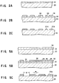
- FIGS. 1A to 1C are views for explaining the principle (the resolution when patterns are projected onto a wafer to expose the wafer) of a halftone phase shift mask.
- FIG. 1A is a view schematically showing the mask.
- a semitransparent halftone film 12 having patterns formed in accordance with the patterns to be projected is formed on a transparent quartz glass substrate 10.
- a semitransparent halftone film 12 having patterns formed in accordance with the patterns to be projected is formed on a transparent quartz glass substrate 10.
- about 2 to 15% of light 14 is transmitted through the halftone film 12 although the amplitude attenuates.
- nearly 100% of light 16 is transmitted only through the glass substrate 10 without transmitted through the halftone film 12. Accordingly, the amplitude distribution of the exposure light on the wafer is as shown in FIG. 1B.
- the amplitudes of the lights 14 and 16 have opposite polarities. Since the square of the amplitude of light is proportional to the light intensity, the intensity distribution of the exposure light projected onto the wafer surface is as shown in FIG. 1C, and the light intensity at the boundaries of the pattern (the edge of the halftone film 12) is 0. Consequently, the edge contrast of the patterns improves, and this improves the resolution of the patterns. Furthermore, as a similar effect is obtained both before and after the focal point, the resolution increases even if the focal point somewhat gets out of position. The result is an effect of improving the focusing margin.
- a halftone phase shift mask according to the first embodiment will be described below with reference to FIGS. 2A to 2C.
- This mask is for KrF excimer laser exposure.
- argon (Ar) gas and oxygen (O 2 ) gas are introduced into a chamber, and a halftone film 22 made of a zirconium oxide is formed on a transparent quartz glass substrate 20 by reactive sputtering using a zirconium compound target.
- Optical conditions of the halftone film 22 are so determined that the transmittance to exposure light is 2 to 15%, the phase of light transmitted through the film is shifted 180° from the phase of light not transmitted through the film, the reflectance to exposure light is 30% or less, and the transmittance to light for mask inspection is 30% or less. Consequently, a phase shift mask blank as shown in FIG. 2A is manufactured.
- the refractive index of the substrate 20 be n s
- the refractive index, extinction coefficient, and film thickness of the halftone film 22 be n, k, and d, respectively
- the refractive index of air be n o .
- phase shift is also important as well as T and R.
- T and R the argument of a complex transmittance t must be used.
- PS 2 ⁇ (n - 1)d/ ⁇
- the film formation conditions of the halftone film 22 shown in FIG. 2A are as follows.
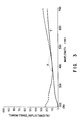
- FIG. 3 shows the spectral transmittance T characteristic and the spectral reflectance R characteristic of a halftone phase shift mask blank having a zirconium oxide compound film formed under the above film formation conditions.
- Film thickness d is set to 980 ⁇ according to equation (3) to have a phase shift of 180°.
- the blank has flat characteristics over a broad wavelength region.
- the spectral transmittance at 248 nm as the exposure light wavelength is 5.1%
- the transmittance to the e-line (wavelength: 546 nm) of a high-pressure mercury lamp as inspection light is 14.8%
- the transmittance to an He-Ne laser beam (wavelength: 633 nm) as another inspection light is about 18%
- the transmittance to an Ar laser beam (wavelength: 488 nm) as still another inspection light is about 13%. Accordingly, sufficient contrast can be obtained during inspection.
- the reflectance at the wavelength 248 nm of the exposure light is 16.9%. Consequently, it is possible to prevent the influence of multiple reflection during exposure and obtain a satisfactory value.
- an electron-beam resist is coated by a spinner to form an electron-beam resist layer 24, and a predetermined pattern is drawn by an electron beam and developed to form a resist pattern 24 having apertures 26 (FIG. 2B).
- the sheet resistance of the zirconium oxide compound film formed under the film formation conditions described above is 1.43 ⁇ 10 4 ⁇ / ⁇ . Accordingly, charge-up during the electron-beam lithography posed almost no problem.
- phase shift mask blank (FIG. 2B) having the resist pattern is patterned by dry etching. Thereafter, the electron-beam resist layer 24 is removed to obtain a halftone phase shift mask having a halftone pattern 22a (FIG. 2C).
- zirconium oxide is used as a halftone film in the above description, the same effect can be obtained by using general zirconium compounds.
- the halftone phase shift mask blank of this embodiment has a structure in which a halftone film made from a thin zirconium compound is formed on a transparent glass substrate.
- the values of the optical constants (the refractive index n, the extinction coefficient k, and the film thickness d) of the halftone film are so selected as to achieve a reflectance of 30% or less at the exposure light wavelength and a transmittance of 30% or less at the inspection light wavelength, in addition to the standard optical conditions for the phase shift mask (the transmittance of exposure light transmitted through the halftone film: 2 to 15%, the phase shift between light transmitted through the halftone film and light not transmitted through the film: 180°).
- the halftone film has a transmittance of 30% or less at the wavelength of visible light (e.g., a high-pressure mercury lamp e-line (546 nm) or an Ar ion laser beam (488 nm)) used in tests. Therefore, enough contrast can be obtained during the inspection. Also, the reflectance to the KrF laser wavelength is less than 30%. This prevents the pattern accuracy from being decreased due to multiple reflection occurring between the halftone layer and the wafer during photolithography. Since there is no influence of multiple reflection, no antireflection layer is necessary. Additionally, inspection and size measurement of the mask can be easily performed because the contrasts during the inspection and measurement are satisfactory.
- visible light e.g., a high-pressure mercury lamp e-line (546 nm) or an Ar ion laser beam (488 nm)
- a zirconium compound film has sufficient conductivity (sheet resistance 100 M ⁇ / ⁇ or less), it is possible to prevent charge-up during electron-beam lithography and improve the pattern formation accuracy. Analogously, this conductivity eliminates charging of static electricity and prevents easy adhesion of dust during manufacturing steps of the mask or when the mask is in use. Also, a zirconium film is hard, so it is possible to reduce defects caused by damage or marring in the step of manufacturing the phase shift mask or the test step and achieve sufficient durability against sulfuric acid in the cleaning step. Furthermore, since the film is a single metal compound, the film has high pattern formation accuracy and high pattern shape reproducibility.
- This second embodiment uses a zirconium silicide compound, e.g., a zirconium oxide silicide film, instead of a zirconium compound, as a halftone film.
- This mask is an i-line exposure mask.
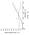
- FIG. 4 shows the spectral transmittance T characteristic and the spectral reflectance R characteristic of a halftone phase shift mask blank having a zirconium oxide silicide film formed under the above film formation conditions.
- the blank has flat characteristics over a broad wavelength region.
- the spectral transmittance at 365 nm as the exposure light wavelength is 8.0%
- the transmittance to an Ar ion laser beam (wavelength: 488 nm) as inspection light is 20.9%
- the transmittance to the e-line (wavelength: 546 nm) of a high-pressure mercury lamp as another inspection light is about 28%. Accordingly, sufficient contrast can be obtained during inspection.
- the reflectance at the wavelength 365 nm of the exposure light is 16.9%. Consequently, it is possible to prevent the influence of multiple reflection during exposure and obtain a satisfactory value.
- the sheet resistance is 5.52 ⁇ 10 6 ⁇ / ⁇ , so charge-up during the electron-beam lithography posed almost no problem.
- the halftone film in the second embodiment is not limited to zirconium oxide silicide.
- zirconium nitride silicide zirconium oxynitride silicide, zirconium oxycarbide silicide, zirconium carbonitride silicide, zirconium halide silicide (e.g., zirconium fluoride silicide and zirconium chloride silicide), zirconium halide oxide silicide (e.g., zirconium fluoride oxide silicide and zirconium chloride oxide silicide), and zirconium halide nitride silicide (e.g., zirconium fluoride nitride silicide and zirconium chloride nitride silicide).
- the halftone phase shift mask blank of the second embodiment has a structure in which a halftone film made from a thin zirconium oxide silicide compound film having an aperture pattern is formed on a transparent glass substrate.
- the values of the optical constants (the refractive index n, the extinction coefficient k, and the film thickness d) of the halftone film are so selected as to achieve a reflectance of 30% or less at an exposure light wavelength and a transmittance of 30% or less at the inspection light wavelength, in addition to the standard optical conditions for the phase shift mask (the transmittance of exposure light transmitted through the halftone film: 2 to 15%, the phase shift between light transmitted through the halftone film and light not transmitted through the film: 180°).
- the halftone film has a transmittance of 30% or less at the wavelength of visible light (e.g., a high-pressure mercury lamp e-line (546 nm) or an Ar ion laser beam (488 nm)) used in inspection. Therefore, enough contrast can be obtained during the inspection. Also, the reflectance to the i-line wavelength (365 nm) is less than 30%. This prevents the pattern accuracy from being decreased due to multiple reflection occurring between the halftone layer and the wafer during photolithography. Since there is no influence of multiple reflection, no antireflection layer is necessary. Additionally, inspection and size measurement of the mask can be easily performed because the contrasts during the inspection and measurement are satisfactory.
- visible light e.g., a high-pressure mercury lamp e-line (546 nm) or an Ar ion laser beam (488 nm)
- a zirconium oxide compound film has sufficient conductivity (sheet resistance 100 M ⁇ / ⁇ or less), it is possible to prevent charge-up during electron-beam lithography and improve the pattern formation accuracy. Analogously, this conductivity eliminates charging of static electricity and prevents easy adhesion of dust during manufacturing steps of the mask or when the mask is in use. Also, a zirconium silicide film is hard, so it is possible to reduce defects caused by damage or marring in the step of manufacturing a phase shift mask or the test step and achieve sufficient durability against sulfuric acid in the cleaning step. Furthermore, since the film is a single metal compound, the film has high pattern formation accuracy and high pattern shape reproducibility.
- phase shift masks having single-layer halftone films made of a zirconium oxide and a zirconium oxide silicide, respectively, have been explained.
- a light-shielding film is additionally formed on these halftone films.
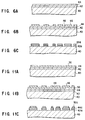
- FIGS. 5A to 5C show manufacturing steps of a mask obtained by forming a light-shielding film in the first embodiment.
- argon (Ar) gas and oxygen (O 2 ) gas are introduced into a chamber, and a halftone film 22 made of a zirconium oxide is formed on a transparent quartz glass substrate 20 by reactive sputtering using a zirconium compound target.
- a light-shielding film 30 is formed on the halftone film 22.
- This light-shielding film 30 is made from a single metal layer or a plurality of layers of a metal and a metal compound (for lowering the reflectance). Cr, Zr, ZrSi, Mo, MoSi, Ta, TaSi, or the like is used as a metal, and an oxide, a nitride, a carbide, or a halide (a fluoride or a chloride) is used as a metal compound.
- phase shift mask blank as shown in FIG. 5A is manufactured.
- the film formation conditions and optical constants of the halftone film 22 shown in FIG. 5A are the same as in the first embodiment.
- a halftone film pattern is drawn on the halftone mask blank with the light-shielding layer by an electron beam and developed to form a resist pattern 24 having apertures 26 (FIG. 5B).
- the light-shielding film 30 is dry etched with the resist pattern 24 and the halftone film 22 is dry etched with the light-shielding pattern as the mask.
- the electron-beam resist layer is coated on the entire surface of the light-shielding film 30. After the light-shielding pattern is drawn by an electron beam and developed, the light-shielding film 30 is dry etched with the resist pattern to remove the electron-beam resist layer.
- the halftone phase shift mask with a light-shielding film 30a having a halftone pattern 22a (FIG. 5C).
- the manufacturing method of the halftone phase shift mask is not limited to the above method.
- the light-shielding pattern is drawn by an electron beam on the halftone phase shift mask blank with the light-shielding film and the blank is developed to form the resist pattern.
- the light-shielding film is dry etched with the resist pattern and the resist is removed.
- the electron-beam resist layer is coated on the entire surface of the light-shielding film.
- the halftone film pattern is drawn by an electron beam and developed, the halftone film is dry etched with the resist pattern to remove the electron-beam resist layer.
- the halftone film of the halftone phase shift mask is light shielded at the portion except the edge portion thereof. It is required for the halftone film to have transmittance about 2 to 15%. However, it is not necessary to have transmittance of this level except the edge portion of the halftone pattern. Therefore, the edge of the light-shielding film 30a is located inside the edge by a distance w.
- the optimum distance w depends on the width d of the pattern. The reason why the light-shielding film is used is to improve the resolution of the fine pattern by using the phase shift technique. It is not necessary to use the phase shift technique for the rough pattern with a large pattern width. For the pattern having a large width, it is possible to set the distance w at 0.
- a mask manufactured by forming a light-shielding film in the second embodiment has the same effect as the third embodiment.
- the above embodiments relate to a phase shift mask having a single-layer halftone film.
- the present invention is also applicable to a mask having a multi-layer halftone film.
- Embodiments in which the halftone films of the first to third embodiments are replaced with multi-layer films will be described below.
- the fourth embodiment is a mask for KrF excimer laser exposure.
- argon (Ar) gas at a flow rate: 20 SCCM, oxygen (O 2 ) gas at a flow rate: 3 SCCM, and N 2 gas at a flow rate: 4 SCCM are introduced into a chamber, and a first halftone film 42 made from a zirconium oxynitride film having a thickness d of 622 ⁇ is formed on a transparent quartz glass substrate 40 by reactive sputtering using a zirconium compound target.
- the halftone film 42 has a refractive index n of 2.20 and an extinction coefficient k of 0.21 at an exposure light wavelength of 248 nm.
- argon (Ar) gas at a flow rate: 20 SCCM and oxygen (O 2 ) gas at a flow rate: 2 SCCM are introduced into a chamber, and a second halftone film 44 made from a zirconium oxide compound film having a thickness d of 624 ⁇ is formed on the zirconium oxynitride film 42 by reactive sputtering using a zirconium compound target.
- the halftone film 44 has a refractive index n of 1.79 and an extinction coefficient k of 0.72 at an exposure light wavelength of 248 nm.
- T and R can be calculated by directly using equations (1) and (2) as in the case of a single-layer film.
- the transmittance characteristics of the first and second halftone films are so chosen that the transmittance characteristic of the first halftone film (close to the substrate) is more transparent than a desired transmittance characteristic, the transparent characteristic of the second halftone film is more opaque than the desired transmittance characteristic, and the desired transmittance characteristic is obtained when they are synthesized. If the total sheet resistance of the multi-layer halftone film is lower that 100 M ⁇ / ⁇ , it is possible to reverse the above relationship. That is, the transmittance characteristic of the first halftone film is more opaque than a desired transmittance characteristic and the transmittance characteristic of the second halftone film is more transparent than the desired transmittance characteristic. In the fourth embodiment, it is possible to reverse the above relationship since the extinction coefficient k of the first halftone layer is 0.21.
- FIG. 7 shows the spectral transmittance T characteristic and the spectral reflectance R characteristic of the shift mask blank shown in FIG. 6A.
- the transmittance at the exposure light wavelength (the wavelength of a KrF excimer laser: 248 nm) is 5%, and the transmittance at the inspection light wavelength (488 nm) is 15.7%. Accordingly, sufficient contrast can be obtained during inspection. Also, the reflectance at the wavelength 248 nm of the exposure light is 12.2%. Consequently, it is possible to prevent the influence of multiple reflection during exposure and obtain a satisfactory value.
- an electron-beam resist is coated by a spinner to form an electron-beam resist layer 46, and a predetermined pattern is drawn by an electron beam and developed to form a resist pattern having apertures 48 (FIG. 6B).
- the sheet resistance of the second halftone film 44 made from a zirconium oxide compound film is 3.43 ⁇ 10 3 ⁇ / ⁇ . Accordingly, charge-up during the electron-beam lithography posed almost no problem.
- phase shift mask blank (FIG. 6B) having the resist pattern is patterned by dry etching using a halogen gas such as SiCl 4 , SF 6 , or CF 4
- the electron-beam resist layer 46 is removed to obtain a halftone phase shift mask having halftone patterns 42a and 44a (FIG. 6C).
- the dry etching conditions are that the pressure is 30 mTorr, the power is 300W, and the flow rate of SiCl 4 gas is 50 SCCM.
- zirconium oxide and a zirconium oxynitride film is used as a halftone film in the above description, the same effect can be obtained by using general zirconium compounds.
- the halftone phase shift mask blank of this embodiment has a structure in which a halftone film made from a multi-layer thin zirconium compound films having aperture patterns is formed on a transparent glass substrate.
- the values of the optical constants (the refractive index n, the extinction coefficient k, and the film thickness d) of the halftone film are so selected as to achieve a reflectance of 30% or less at the exposure light wavelength and a transmittance of 30% or less at the inspection light wavelength, in addition to the optical conditions for the phase shift mask (the transmittance of exposure light transmitted through the halftone film: 2 to 15%, the phase shift between light transmitted through the halftone film and light not transmitted through the film: 180°).
- the halftone film has a transmittance of 30% or less at the wavelength of visible light (e.g., a high-pressure mercury lamp e-line (546 nm) or an Ar ion laser beam (488 nm)) used in inspection. Therefore, enough contrast can be obtained during the inspection. Also, the reflectance to the KrF laser wavelength is less than 30%. This prevents the pattern accuracy from being decreased due to multiple reflection occurring between the halftone layer and the wafer during photolithography. Since there is no influence of multiple reflection, no antireflection layer is necessary. Additionally, inspection and size measurement of the mask can be easily performed because the contrasts during the inspection and measurement are satisfactory.
- visible light e.g., a high-pressure mercury lamp e-line (546 nm) or an Ar ion laser beam (488 nm)
- a zirconium compound film has a sufficient conductivity (sheet resistance 100M ⁇ / ⁇ or less), it is possible to prevent charge-up during electron-beam lithography and improve the pattern formation accuracy. Analogously, this conductivity eliminates charging of static electricity and prevents easy adhesion of dust during manufacturing steps of the mask or when the mask is in use. Also, a zirconium film is hard, so it is possible to reduce defects caused by damage or marring in the step of manufacturing the phase shift mask or the test step and achieve sufficient durability against sulfuric acid in the cleaning step. Furthermore, since the film is a single metal compound, the film has high pattern formation accuracy and high pattern shape reproducibility.
- the fifth embodiment which uses a multi-layer film of the same kind as in the fourth embodiment and having different optical constants will be described below.
- the fifth embodiment is a mask for ArF, laser exposure.
- argon (Ar) gas at a flow rate: 14 SCCM, oxygen (O 2 ) gas at a flow rate: 8 SCCM, and nitrogen (N 2 ) gas at a flow rate: 8 SCCM are introduced into a chamber, and a first halftone film made from a 345 ⁇ thick zirconium oxynitride film is formed on a transparent quartz glass substrate by reactive sputtering using a zirconium compound target.
- the first halftone film has a refractive index of 2.80 and an extinction coefficient of 0.33 at an exposure light wavelength of 193 nm.
- argon (Ar) gas at a flow rate: 20 SCCM and oxygen (O 2 ) gas at a flow rate: 2 SCCM are introduced into a chamber, and a second halftone film made from a 299 ⁇ thick zirconium oxide compound film is formed on the zirconium oxynitride film by reactive sputtering using a zirconium compound target.
- the second halftone film has a refractive index of 2.15 and an extinction coefficient of 1.08 at an exposure light wavelength of 193 nm.
- FIG. 8 shows the spectral transmittance T characteristic and the spectral reflectance R characteristic of the shift mask blank of the fifth embodiment.
- Exposure is performed by an ArF excimer laser.
- the transmittance at the exposure light wavelength (193 nm) is 5%
- the transmittance at the inspection light wavelength (488 nm) is 15.7%. Accordingly, sufficient contrast can be obtained during inspection.
- the reflectance at the wavelength 248 nm of the exposure light is 12.2%. Consequently, it is possible to prevent the influence of multiple reflection during exposure and obtain a satisfactory value.
- the sixth embodiment uses a zirconium silicide compound, e.g., a zirconium oxide silicide film, instead of a zirconium compound, as a multi-layer halftone film.
- the sixth embodiment is a mask for KrF excimer laser exposure.
- the manufacturing steps are the same as in the fourth embodiment shown in FIGS. 6A to 6C.
- argon (Ar) gas and oxygen (O 2 ) gas are introduced into a chamber, and first and second halftone films made from two zirconium oxide silicide films are formed, such that the transmittance is 6% when the phase shift is 180°, on a transparent quartz glass substrate by reactive sputtering using a zirconium silicide target.
- the film thickness of the first halftone film is 600 ⁇ , and that of the second halftone film 480 ⁇ .
- the film formation conditions of the first and second halftone films are as follows. A film farther from the substrate is the second halftone film. Film formation conditions of first halftone film
- FIG. 9 shows the spectral transmittance characteristic and the spectral reflectance characteristic of a halftone phase shift mask blank made from zirconium oxide silicide films formed under the above film formation conditions.
- the mask has flat characteristics over a broad wavelength region.
- the spectral transmittance at 248 nm as the wavelength of a KrF excimer laser as exposure light is 6.7%, and the transmittance at a inspection light wavelength of 546 nm is 26.8%. Accordingly, sufficient contrast can be obtained during inspection.
- the reflectance at the wavelength 248 nm of the exposure light is 24.7%. Consequently, it is possible to prevent the influence of multiple reflection during exposure and obtain a satisfactory value.
- the sheet resistance of the zirconium oxide silicide film is 3.33 k ⁇ / ⁇ . Accordingly, charge-up during the electron-beam lithography posed almost no problem.
- the seventh embodiment which uses a multi-layer film of the same kind as in the sixth embodiment and having different optical constants will be described below.
- the seventh embodiment is a halftone phase shift mask blank for ArF excimer laser exposure.
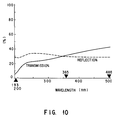
- FIG. 10 shows the spectral transmittance T characteristic and the spectral reflectance R characteristic of the shift mask blank of the seventh embodiment.
- Exposure is performed by an ArF excimer laser.
- the transmittance at the exposure light wavelength (193 nm) is 5%
- the transmittance at the inspection light wavelength (365 nm) is about 29%. Accordingly, sufficient contrast can be obtained during inspection.
- the reflectance at the wavelength 193 nm of the exposure light is about 28%. Consequently, it is possible to prevent the influence of multiple reflection during exposure and obtain a satisfactory value.
- the thickness of the first halftone film is set to 830 ⁇ and that of the second halftone film is set to 210 ⁇ according to equation (4).
- FIGS. 11A to 11C show manufacturing steps of a mask obtained by forming a light-shielding film in the fourth embodiment.
- This light-shielding film 50 is made from a single metal layer or a plurality of layers of a metal and a metal compound (for lowering the reflectance). Cr, Zr, ZrSi, Mo, MoSi, Ta, TaSi, or the like is used as a metal, and an oxide, a nitride, a carbide, or a halide (a fluoride or a chloride) is used as a metal compound.
- the phase shift mask blank as shown in FIG. 11A is manufactured.
- the film formation conditions and optical constants of the halftone films 42 and 44 shown in FIG. 11A are the same as in the fourth embodiment.
- the manufacturing method for the phase shift mask having the light-shielding film is the same as in the third embodiment shown in FIGS. 5A to 5C. Therefore, it is possible to set the distance w at 0 for the pattern having a large width.
- masks manufactured by forming a light-shielding film in the fifth to seventh embodiments have the same effect as the eighth embodiment.
- the present invention is not limited to the above embodiments and can be practiced in the form of various modifications.
- the substrate is not limited to a quartz glass.
- a calcium fluoride may be used as the substrate for an ArF laser exposure blank or mask.
- An RF sputtering apparatus may be instead of the DC sputtering apparatus.
- Inert gas used in the sputtering apparatus may include xenon gas, nitrogen gas, nitrogen oxide gas, nitrogen dioxide gas, or halogen gas.
- a halftone film made from a thin zirconium compound film is formed on a transparent substrate, and the values of the refractive index n, the extinction coefficient k, and the film thickness d of the zirconium compound film are so selected as to achieve a reflectance of 30% or less at the exposure light wavelength and a transmittance of 30% or less at the inspection light wavelength, in addition to the optical conditions for the halftone phase shift mask (the transmittance of exposure light transmitted through the halftone film: 2 to 15%, the phase shift between light transmitted through the halftone film and light not transmitted through the film but only through the substrate: 180° ). Therefore, enough contrast can be obtained during the inspection. Also, the reflectance to the exposure light wavelength is less than 30%.
- a zirconium film is hard, so it is possible to reduce defects caused by damage or marring in the step of manufacturing the phase shift mask or the test step and achieve sufficient durability against sulfuric acid in the cleaning step. Furthermore, since the film is a single metal compound, the film has high pattern formation accuracy and high pattern shape reproducibility.
- a quartz glass substrate (10) is placed in a DC or RF sputtering apparatus containing argon gas or oxygen gas.
- a zirconium compound target is reactively sputtered to form at least one halftone film (12), made of a zirconium compound target on the substrate, thereby forming a blank for a halftone phase shift mask.
- the refractive index, the extinction coefficient, and the film thickness of the halftone film are so determined that the transmittance and the reflectance to exposure light are 2 to 15% and 30% or less, respectively, and the transmittance to inspection light is 30% or less.
- zirconium compound examples include zirconium oxide, zirconium nitride, zirconium oxynitride, zirconium oxycarbide, zirconium carbonitride, zirconium halide, zirconium halide oxide, zirconium halide nitride, zirconium oxide silicide, zirconium nitride silicide, zirconium oxynitride silicide, zirconium oxycarbide silicide, zirconium carbonitride silicide, zirconium halide silicide, zirconium halide oxide silicide, and zirconium halide nitride silicide.
Abstract


Description
- r is the complex conjugate of r
-
-
-
-
- I is an imaginary number unit.
Where


Film formation conditions of first halftone film
- Power: 200W
- Pressure: 0.43 Pa
- Flow rate ratio of Ar gas to O2 gas: 90/10
This prevents the pattern accuracy from being decreased due to multiple reflection occurring between the halftone layer and the wafer during photolithography. Since there is no influence of multiple reflection, no antireflection layer is necessary. Additionally, inspection and size measurement of the mask can be easily performed because the contrasts during the inspection and measurement are satisfactory. Furthermore, since a zirconium compound film has sufficient conductivity, it is possible to prevent charge-up during electron-beam lithography and improve the pattern formation accuracy. Analogously, this conductivity eliminates charging of static electricity and prevents easy adhesion of dust during manufacturing steps of the mask or when the mask is in use. Also, a zirconium film is hard, so it is possible to reduce defects caused by damage or marring in the step of manufacturing the phase shift mask or the test step and achieve sufficient durability against sulfuric acid in the cleaning step. Furthermore, since the film is a single metal compound, the film has high pattern formation accuracy and high pattern shape reproducibility.
Claims (40)
- A blank for a halftone phase shift mask, characterized by comprising:a transparent substrate (10); anda halftone film (12) formed on said substrate and made of a zirconium compound, said halftone film giving a phase shift of 180° between light transmitted through the halftone film and light not transmitted through the halftone film.
- A blank according to claim 1, characterized in that said halftone film is a single-layer film (22).
- A blank according to claim 1, characterized in that said halftone film is a two-layer film (42, 44).
- A blank according to claim 1, characterized in that said zirconium compound is zirconium oxide, zirconium nitride, zirconium oxynitride, zirconium oxycarbide, zirconium carbonitride, zirconium halide, zirconium halide oxide, or zirconium halide nitride.
- A blank according to claim 4, characterized in that said halide is a fluoride or a chloride.
- A blank according to claim 1, characterized in that said zirconium compound is a zirconium silicide compound.
- A blank according to claim 6, characterized in that said zirconium silicide compound is zirconium oxide silicide, zirconium nitride silicide, zirconium oxynitride silicide, zirconium oxycarbide silicide, zirconium carbonitride silicide, zirconium halide silicide, zirconium halide oxide silicide, or zirconium halide nitride silicide.
- A blank according to claim 7, characterized in that said halide is a fluoride or a chloride.
- A blank according to claim 1, characterized by further comprising a light-shielding layer (30) on said halftone film.
- A blank according to claim 9, characterized in that said light-shielding layer is a single-layer film of a metal.
- A blank according to claim 9, characterized in that said light-shielding layer is a multi-layer film of a metal and a metal compound.
- A blank according to claim 10 or 11, characterized in that said metal layer is made of chromium, zirconium or zirconium silicide, Mo, MoSi, Ta, or TaSi.
- A blank according to claim 11, characterized in that said compound is an oxide, a nitride, a oxynitride, a oxycarbide, a carbonitride, a halide, a halide oxide, or a halide nitride.
- A blank according to claim 13, characterized in that said halide is a fluoride or a chloride.
- A blank according to claim 1, characterized in that said halftone film has a transmittance of 2 to 15% and a reflectance of not more than 30% to an exposure light, and a transmittance of not more than 30% to a inspection light.
- A blank according to claim 1, characterized in that a refractive index, an extinction coefficient, and a film thickness of said halftone film are so set to obtain a transmittance and a reflectance to an exposure light of 2 to 15% and not more than 30%, respectively, and a transmittance to a inspection light of not more than 30%.
- A blank according to claim 1, characterized in that said halftone film has a conductivity of not more than 100 M Ω/□.
- A blank according to claim 1, characterized in that said substrate is a quartz glass or a calcium fluoride.
- A halftone phase shift mask characterized by comprising:a transparent substrate (10); anda patterned halftone film (12) formed on said substrate and made of a zirconium compound, said halftone film giving a phase shift of 180° between light transmitted through the halftone film and light not transmitted through the halftone film.
- A mask according to claim 19, characterized in that said halftone film is a single-layer film (22).
- A mask according to claim 19, characterized in that said halftone film is a two-layer film (42, 44).
- A mask according to claim 19, characterized in that said zirconium compound is zirconium oxide, zirconium nitride, zirconium oxynitride, zirconium oxycarbide, zirconium carbonitride, zirconium halide, zirconium halide oxide, or zirconium halide nitride.
- A mask according to claim 22, characterized in that said halide is a fluoride or a chloride.
- A mask according to claim 19, characterized in that said zirconium compound is a zirconium silicide compound.
- A mask according to claim 24, characterized in that said zirconium silicide compound is zirconium oxide silicide, zirconium nitride silicide, zirconium oxynitride silicide, zirconium oxycarbide silicide, zirconium carbonitride silicide, zirconium halide silicide, zirconium halide oxide silicide, or zirconium halide nitride silicide.
- A mask according to claim 25, characterized in that said halide is a fluoride or a chloride.
- A mask according to claim 19, characterized by further comprising a light-shielding layer (30) on said halftone film.
- A mask according to claim 27, characterized in that said light-shielding layer is a single-layer film of a metal.
- A mask according to claim 27, characterized in that said light-shielding layer is a multi-layer film of a metal and a metal compound.
- A mask according to claim 28 or 29, characterized in that said metal layer is made of chromium, zirconium or zirconium silicide, Mo, MoSi, Ta, or TaSi.
- A mask according to claim 29, characterized in that said compound is an oxide, a nitride, a oxynitride, a oxycarbide, a carbonitride, a halide, a halide oxide, or a halide nitride.
- A mask according to claim 31, characterized in that said halide is a fluoride or a chloride.
- A mask according to claim 19, characterized in that said halftone film has a transmittance of 2 to 15% and a reflectance of not more than 30% to an exposure light, and a transmittance of not more than 30% to a inspection light.
- A mask according to claim 19, characterized in that a refractive index, an extinction coefficient, and a film thickness of said halftone film are so set to obtain a transmittance and a reflectance to an exposure light of 2 to 15% and not more than 30%, respectively, and a transmittance to a inspection light of not more than 30%.
- A mask according to claim 19, characterized in that said halftone film has a conductivity of not more than 100 M Ω/□.
- A mask according to claim 19, characterized in that said substrate is a quartz glass or a calcium fluoride.
- A method of manufacturing a blank for a halftone phase shift mask, characterized in that a transparent substrate (10) is placed in a sputtering apparatus containing inert gas, and a zirconium compound target is reactively sputtered to form at least one halftone film (12) made of a zirconium compound on said substrate.
- A method according to claim 37, characterized in that a light-shielding film is further formed on said halftone film.
- A method of manufacturing a halftone phase shift mask, characterized by comprising the steps of:placing a transparent substrate (20) in a sputtering apparatus containing inert gas, and reactively sputtering a zirconium compound target to form at least one halftone film (22) made of a zirconium compound on said substrate, thereby forming a blank for a halftone phase shift mask;forming a resist pattern (24) corresponding to an exposure pattern on said halftone film; andremoving said resist pattern (24) by etching.
- A method according to claim 39, characterized in that a light-shielding film is further formed on said halftone film.
Applications Claiming Priority (4)
| Application Number | Priority Date | Filing Date | Title |
|---|---|---|---|
| JP282409/96 | 1996-10-24 | ||
| JP28240996 | 1996-10-24 | ||
| JP322521/96 | 1996-12-03 | ||
| JP32252196A JPH10161294A (en) | 1996-12-03 | 1996-12-03 | Halftone phase shift mask blank, halftone phase shift mask and its production |
Publications (2)
| Publication Number | Publication Date |
|---|---|
| EP0838726A1 true EP0838726A1 (en) | 1998-04-29 |
| EP0838726B1 EP0838726B1 (en) | 2012-02-29 |
Family
ID=26554599
Family Applications (1)
| Application Number | Title | Priority Date | Filing Date |
|---|---|---|---|
| EP97118464A Expired - Lifetime EP0838726B1 (en) | 1996-10-24 | 1997-10-23 | Halftone phase shift mask, blank for the same, and methods of manufacturing these |
Country Status (4)
| Country | Link |
|---|---|
| US (1) | US5935735A (en) |
| EP (1) | EP0838726B1 (en) |
| KR (1) | KR100505494B1 (en) |
| TW (1) | TW346556B (en) |
Cited By (6)
| Publication number | Priority date | Publication date | Assignee | Title |
|---|---|---|---|---|
| EP1116999A1 (en) * | 2000-01-05 | 2001-07-18 | Shin-Etsu Chemical Co., Ltd. | Phase shift mask blank, phase shift mask and method of manufacture |
| EP1152292A2 (en) * | 2000-04-27 | 2001-11-07 | Dai Nippon Printing Co., Ltd. | Halftone phase shift photomask and blank for halftone phase shift photomask |
| EP1176465A2 (en) * | 2000-07-25 | 2002-01-30 | International Business Corporation | A ternary photomask and method of making the same |
| US6576374B1 (en) | 1999-07-02 | 2003-06-10 | Samsung Electronics Co., Ltd. | Mask blank and method of fabricating phase shift mask from the same |
| EP1582921A2 (en) * | 2004-03-31 | 2005-10-05 | Shin-Etsu Chemical Co., Ltd. | Film-depositing target and preparation of phase shift mask blank |
| EP1582920A2 (en) * | 2004-03-31 | 2005-10-05 | Shin-Etsu Chemical Co., Ltd. | Halftone phase shifting mask blank, halftone phase shifting mask, and pattern transfer method |
Families Citing this family (29)
| Publication number | Priority date | Publication date | Assignee | Title |
|---|---|---|---|---|
| EP1031877A4 (en) * | 1997-11-11 | 2001-05-09 | Nikon Corp | Photomask, aberration correcting plate, exposure device and method of producing microdevice |
| JP3276954B2 (en) * | 1998-07-31 | 2002-04-22 | ホーヤ株式会社 | Photomask blank, photomask, method for producing them, and method for forming fine pattern |
| WO2000020928A1 (en) | 1998-10-08 | 2000-04-13 | Rochester Institute Of Technology | Photomask for projection lithography at or below about 160 nm and a method |
| US6835505B2 (en) * | 1998-10-08 | 2004-12-28 | Rochester Institute Of Technology | Mask for projection photolithography at or below about 160 nm and a method thereof |
| JP4073569B2 (en) * | 1999-02-03 | 2008-04-09 | セイコーインスツル株式会社 | Recording medium that can be played back using near-field light |
| JP2001201842A (en) * | 1999-11-09 | 2001-07-27 | Ulvac Seimaku Kk | Phase shift photomask blank, phase shift photomask, and manufacturing method of semiconductor device |
| US6694275B1 (en) * | 2000-06-02 | 2004-02-17 | Timbre Technologies, Inc. | Profiler business model |
| US6524755B2 (en) | 2000-09-07 | 2003-02-25 | Gray Scale Technologies, Inc. | Phase-shift masks and methods of fabrication |
| JP2002090977A (en) * | 2000-09-12 | 2002-03-27 | Hoya Corp | Phase shift mask blank, photomask blank as well as manufacturing apparatus and manufacturing method for the same |
| JP2002141512A (en) * | 2000-11-06 | 2002-05-17 | Advanced Display Inc | Patterning method of thin film, tft array substrate using the patterning method, and manufacturing method of the tft array substrate |
| JP2003114514A (en) * | 2001-10-02 | 2003-04-18 | Sharp Corp | Pattern transferring method using mask, halftone mask, its manufacturing method and manufacturing method of circuit substrate |
| US6698008B2 (en) * | 2001-10-30 | 2004-02-24 | International Business Machines Corporation | Row-based placement scoring and legalization measure for books with phase shift mask dependencies |
| KR100815679B1 (en) * | 2001-11-27 | 2008-03-20 | 호야 가부시키가이샤 | Halftone phase shift mask blank, halftone phase shift mask, and manufacturing method thereof |
| DE10307518B4 (en) * | 2002-02-22 | 2011-04-14 | Hoya Corp. | Halftone phase shift mask blank, halftone phase shift mask and method of making the same |
| DE10307545A1 (en) * | 2002-02-22 | 2003-11-06 | Hoya Corp | Crop for halftone phase shift mask and associated phase shift mask |
| AU2003257547A1 (en) * | 2002-08-19 | 2004-03-03 | Hoya Corporation | Mask blank manufacturing method, transfer mask manufacturing method, sputtering target for manufacturing mask blank |
| US6855463B2 (en) * | 2002-08-27 | 2005-02-15 | Photronics, Inc. | Photomask having an intermediate inspection film layer |
| KR20060120613A (en) * | 2003-09-05 | 2006-11-27 | 쇼오트 아게 | Attenuated phase shift mask blank and photomask |
| US7879202B2 (en) * | 2003-12-15 | 2011-02-01 | Guardian Industries Corp. | Scratch resistant coated glass article including carbide layer(s) resistant to fluoride-based etchant(s) |
| US7387816B2 (en) * | 2003-12-15 | 2008-06-17 | Guardian Industries Corp. | Scratch resistant coated glass article including layer(s) resistant to fluoride-based etchant(s), and method of making article using combustion CVD |
| US7566481B2 (en) * | 2003-12-15 | 2009-07-28 | Guardian Industries Corp. | Method of making scratch resistant coated glass article including layer(s) resistant to fluoride-based etchant(s) |
| US7445273B2 (en) * | 2003-12-15 | 2008-11-04 | Guardian Industries Corp. | Scratch resistant coated glass article resistant fluoride-based etchant(s) |
| MXPA06007048A (en) * | 2003-12-18 | 2007-04-17 | Afg Ind Inc | Protective layer for optical coatings with enhanced corrosion and scratch resistance. |
| KR100549268B1 (en) * | 2003-12-31 | 2006-02-03 | 동부아남반도체 주식회사 | Phase Shifting Mask and Manufacturing Method Thereof |
| KR100851922B1 (en) | 2007-08-31 | 2008-08-12 | 주식회사 하이닉스반도체 | Method for fabricating semiconductor device |
| US8003164B2 (en) * | 2008-09-19 | 2011-08-23 | Guardian Industries Corp. | Method of making a scratch-and etch-resistant coated glass article |
| KR101821304B1 (en) * | 2013-05-03 | 2018-01-23 | 어플라이드 머티어리얼스, 인코포레이티드 | Optically tuned hardmask for multi-patterning applications |
| CN108227368A (en) * | 2018-01-17 | 2018-06-29 | 京东方科技集团股份有限公司 | A kind of mask plate, display base plate and display device |
| JP7109996B2 (en) | 2018-05-30 | 2022-08-01 | Hoya株式会社 | MASK BLANK, PHASE SHIFT MASK, AND SEMICONDUCTOR DEVICE MANUFACTURING METHOD |
Citations (8)
| Publication number | Priority date | Publication date | Assignee | Title |
|---|---|---|---|---|
| JPS58173744A (en) | 1982-04-05 | 1983-10-12 | インタ−ナショナル ビジネス マシ−ンズ コ−ポレ−ション | Mask |
| JPS6250811B2 (en) | 1980-09-30 | 1987-10-27 | Nippon Kogaku Kk | |
| US4890309A (en) | 1987-02-25 | 1989-12-26 | Massachusetts Institute Of Technology | Lithography mask with a π-phase shifting attenuator |
| JPH04136854A (en) | 1990-09-28 | 1992-05-11 | Hitachi Ltd | Photomask and production thereof, formation of pattern by using this method and photomask blank |
| EP0668539A2 (en) * | 1994-02-22 | 1995-08-23 | International Business Machines Corporation | Thinfilm materials for the preparation of attenuating phase shift masks |
| JPH0854725A (en) * | 1994-08-11 | 1996-02-27 | Toppan Printing Co Ltd | Halftone type phase shift mask and mask blank used for the same |
| JPH08171196A (en) * | 1994-12-19 | 1996-07-02 | Toppan Printing Co Ltd | Half-ton type phase shift mask, mask blank thereof and production of half-tone type phase shift mask |
| US5547787A (en) * | 1992-04-22 | 1996-08-20 | Kabushiki Kaisha Toshiba | Exposure mask, exposure mask substrate, method for fabricating the same, and method for forming pattern based on exposure mask |
Family Cites Families (2)
| Publication number | Priority date | Publication date | Assignee | Title |
|---|---|---|---|---|
| JP3339649B2 (en) * | 1993-07-30 | 2002-10-28 | 大日本印刷株式会社 | Method for manufacturing blank for halftone phase shift photomask and method for manufacturing halftone phase shift photomask |
| KR200148328Y1 (en) * | 1996-08-09 | 1999-06-15 | 왕중일 | Pll tuner |
-
1997
- 1997-10-22 US US08/954,939 patent/US5935735A/en not_active Expired - Lifetime
- 1997-10-23 TW TW086115684A patent/TW346556B/en not_active IP Right Cessation
- 1997-10-23 EP EP97118464A patent/EP0838726B1/en not_active Expired - Lifetime
- 1997-10-24 KR KR1019970054967A patent/KR100505494B1/en not_active IP Right Cessation
Patent Citations (8)
| Publication number | Priority date | Publication date | Assignee | Title |
|---|---|---|---|---|
| JPS6250811B2 (en) | 1980-09-30 | 1987-10-27 | Nippon Kogaku Kk | |
| JPS58173744A (en) | 1982-04-05 | 1983-10-12 | インタ−ナショナル ビジネス マシ−ンズ コ−ポレ−ション | Mask |
| US4890309A (en) | 1987-02-25 | 1989-12-26 | Massachusetts Institute Of Technology | Lithography mask with a π-phase shifting attenuator |
| JPH04136854A (en) | 1990-09-28 | 1992-05-11 | Hitachi Ltd | Photomask and production thereof, formation of pattern by using this method and photomask blank |
| US5547787A (en) * | 1992-04-22 | 1996-08-20 | Kabushiki Kaisha Toshiba | Exposure mask, exposure mask substrate, method for fabricating the same, and method for forming pattern based on exposure mask |
| EP0668539A2 (en) * | 1994-02-22 | 1995-08-23 | International Business Machines Corporation | Thinfilm materials for the preparation of attenuating phase shift masks |
| JPH0854725A (en) * | 1994-08-11 | 1996-02-27 | Toppan Printing Co Ltd | Halftone type phase shift mask and mask blank used for the same |
| JPH08171196A (en) * | 1994-12-19 | 1996-07-02 | Toppan Printing Co Ltd | Half-ton type phase shift mask, mask blank thereof and production of half-tone type phase shift mask |
Non-Patent Citations (4)
| Title |
|---|
| CARCIA P F ET AL: "MATERIALS SCREENING FOR ATTENUATING EMBEDDED PHASE-SHIFT PHOTOBLANKS FOR DUV AND 193 NM PHOTOLITHOGRAPHY", PROCEEDINGS OF THE SPIE, vol. 2884, 18 September 1996 (1996-09-18), pages 255 - 263, XP002036759 * |
| PATENT ABSTRACTS OF JAPAN vol. 096, no. 006 28 June 1996 (1996-06-28) * |
| PATENT ABSTRACTS OF JAPAN vol. 096, no. 011 29 November 1996 (1996-11-29) * |
| SMITH B W ET AL: "The effects of excimer laser radiation on attenuated phase shift masking materials", OPTICAL MICROLITHOGRAPHY X, SANTA CLARA, CA, USA, 12-14 MARCH 1997, vol. 3051, ISSN 0277-786X, PROCEEDINGS OF THE SPIE - THE INTERNATIONAL SOCIETY FOR OPTICAL ENGINEERING, 1997, SPIE-INT. SOC. OPT. ENG, USA, pages 236 - 244, XP002055644 * |
Cited By (16)
| Publication number | Priority date | Publication date | Assignee | Title |
|---|---|---|---|---|
| US6576374B1 (en) | 1999-07-02 | 2003-06-10 | Samsung Electronics Co., Ltd. | Mask blank and method of fabricating phase shift mask from the same |
| EP1116999A1 (en) * | 2000-01-05 | 2001-07-18 | Shin-Etsu Chemical Co., Ltd. | Phase shift mask blank, phase shift mask and method of manufacture |
| US6511778B2 (en) | 2000-01-05 | 2003-01-28 | Shin-Etsu Chemical Co., Ltd. | Phase shift mask blank, phase shift mask and method of manufacture |
| EP1152292A2 (en) * | 2000-04-27 | 2001-11-07 | Dai Nippon Printing Co., Ltd. | Halftone phase shift photomask and blank for halftone phase shift photomask |
| EP1152292A3 (en) * | 2000-04-27 | 2002-07-31 | Dai Nippon Printing Co., Ltd. | Halftone phase shift photomask and blank for halftone phase shift photomask |
| US6599667B2 (en) | 2000-04-27 | 2003-07-29 | Dai Nippon Printing Co., Ltd. | Halftone phase shift photomask and blank for halftone phase shift photomask |
| EP1176465A2 (en) * | 2000-07-25 | 2002-01-30 | International Business Corporation | A ternary photomask and method of making the same |
| EP1176465A3 (en) * | 2000-07-25 | 2002-08-07 | International Business Corporation | A ternary photomask and method of making the same |
| EP1582921A2 (en) * | 2004-03-31 | 2005-10-05 | Shin-Etsu Chemical Co., Ltd. | Film-depositing target and preparation of phase shift mask blank |
| EP1582920A2 (en) * | 2004-03-31 | 2005-10-05 | Shin-Etsu Chemical Co., Ltd. | Halftone phase shifting mask blank, halftone phase shifting mask, and pattern transfer method |
| EP1582920A3 (en) * | 2004-03-31 | 2006-08-09 | Shin-Etsu Chemical Co., Ltd. | Halftone phase shifting mask blank, halftone phase shifting mask, and pattern transfer method |
| EP1582921A3 (en) * | 2004-03-31 | 2007-05-30 | Shin-Etsu Chemical Co., Ltd. | Film-depositing target and preparation of phase shift mask blank |
| EP1813983A2 (en) * | 2004-03-31 | 2007-08-01 | Shin-Etsu Chemical Co., Ltd. | Halftone phase shift mask blank , halftone phase shift mask, and pattern transfer method |
| EP1813983A3 (en) * | 2004-03-31 | 2007-10-24 | Shin-Etsu Chemical Co., Ltd. | Halftone phase shifting mask blank, halftone phase shifting mask, and pattern transfer method |
| US7556892B2 (en) | 2004-03-31 | 2009-07-07 | Shin-Etsu Chemical Co., Ltd. | Halftone phase shift mask blank, halftone phase shift mask, and pattern transfer method |
| US7598004B2 (en) | 2004-03-31 | 2009-10-06 | Shin-Etsu Chemical Co., Ltd. | Film-depositing target and preparation of phase shift mask blank |
Also Published As
| Publication number | Publication date |
|---|---|
| TW346556B (en) | 1998-12-01 |
| EP0838726B1 (en) | 2012-02-29 |
| KR19980033168A (en) | 1998-07-25 |
| US5935735A (en) | 1999-08-10 |
| KR100505494B1 (en) | 2005-10-06 |
Similar Documents
| Publication | Publication Date | Title |
|---|---|---|
| US5935735A (en) | Halftone phase shift mask, blank for the same, and methods of manufacturing these | |
| US5582939A (en) | Method for fabricating and using defect-free phase shifting masks | |
| JP2983020B1 (en) | Halftone type phase shift mask blank and halftone type phase shift mask | |
| US5482799A (en) | Phase shift mask and manufacturing method thereof | |
| KR101333929B1 (en) | Photomask blank, photomask and production method thereof, and semiconductor device production method | |
| US6908715B2 (en) | Multi-layer, attenuated phase-shifting mask | |
| JP3037941B2 (en) | Halftone type phase shift mask and halftone type phase shift mask blank | |
| US20030228529A1 (en) | Photomask and method for repairing defects | |
| US5902702A (en) | Phase shift mask, blank for phase shift mask, and method of manufacturing phase shift mask | |
| TWI778231B (en) | Mask substrate, phase shift mask, and manufacturing method of semiconductor device | |
| JPH10186632A (en) | Blank for halftone type phase shift mask and halftone type phase shift mask | |
| JP3478067B2 (en) | Halftone phase shift mask and blank for halftone phase shift mask | |
| US7049034B2 (en) | Photomask having an internal substantially transparent etch stop layer | |
| JPH06175346A (en) | Production of phase shift mask and phase shift mask blank | |
| JP3645888B2 (en) | Halftone phase shift mask | |
| JP3289606B2 (en) | Blank for halftone type phase shift mask and halftone type phase shift mask | |
| US20050026053A1 (en) | Photomask having an internal substantially transparent etch stop layer | |
| JPH1184624A (en) | Blank for halftone type phase shift mask, halftone type phase shift mask and their production | |
| JPH05265181A (en) | Reticle for reduced projection exposure and blank used for the same | |
| JP3760927B2 (en) | Pattern transfer method | |
| JP4099836B2 (en) | Halftone phase shift mask blank, method of manufacturing the same, and halftone phase shift mask | |
| JP4345333B2 (en) | Phase shift mask and pattern transfer method using the same | |
| JPH10161294A (en) | Halftone phase shift mask blank, halftone phase shift mask and its production | |
| JPH07281414A (en) | Phase shift mask blank and phase shift mask as well as its production | |
| KR100231493B1 (en) | Phase shift mask |
Legal Events
| Date | Code | Title | Description |
|---|---|---|---|
| PUAI | Public reference made under article 153(3) epc to a published international application that has entered the european phase |
Free format text: ORIGINAL CODE: 0009012 |
|
| AK | Designated contracting states |
Kind code of ref document: A1 Designated state(s): DE FR GB IT |
|
| AX | Request for extension of the european patent |
Free format text: AL;LT;LV;RO;SI |
|
| 17P | Request for examination filed |
Effective date: 19980908 |
|
| AKX | Designation fees paid |
Free format text: DE FR GB IT |
|
| RBV | Designated contracting states (corrected) |
Designated state(s): DE FR GB IT |
|
| 17Q | First examination report despatched |
Effective date: 19990611 |
|
| GRAP | Despatch of communication of intention to grant a patent |
Free format text: ORIGINAL CODE: EPIDOSNIGR1 |
|
| GRAS | Grant fee paid |
Free format text: ORIGINAL CODE: EPIDOSNIGR3 |
|
| GRAA | (expected) grant |
Free format text: ORIGINAL CODE: 0009210 |
|
| AK | Designated contracting states |
Kind code of ref document: B1 Designated state(s): DE FR GB IT |
|
| REG | Reference to a national code |
Ref country code: GB Ref legal event code: FG4D |
|
| REG | Reference to a national code |
Ref country code: DE Ref legal event code: R096 Ref document number: 69740380 Country of ref document: DE Effective date: 20120419 |
|
| PLBE | No opposition filed within time limit |
Free format text: ORIGINAL CODE: 0009261 |
|
| STAA | Information on the status of an ep patent application or granted ep patent |
Free format text: STATUS: NO OPPOSITION FILED WITHIN TIME LIMIT |
|
| 26N | No opposition filed |
Effective date: 20121130 |
|
| REG | Reference to a national code |
Ref country code: DE Ref legal event code: R097 Ref document number: 69740380 Country of ref document: DE Effective date: 20121130 |
|
| PGFP | Annual fee paid to national office [announced via postgrant information from national office to epo] |
Ref country code: GB Payment date: 20141022 Year of fee payment: 18 Ref country code: FR Payment date: 20141008 Year of fee payment: 18 Ref country code: DE Payment date: 20141014 Year of fee payment: 18 |
|
| PGFP | Annual fee paid to national office [announced via postgrant information from national office to epo] |
Ref country code: IT Payment date: 20141017 Year of fee payment: 18 |
|
| REG | Reference to a national code |
Ref country code: DE Ref legal event code: R119 Ref document number: 69740380 Country of ref document: DE |
|
| GBPC | Gb: european patent ceased through non-payment of renewal fee |
Effective date: 20151023 |
|
| PG25 | Lapsed in a contracting state [announced via postgrant information from national office to epo] |
Ref country code: IT Free format text: LAPSE BECAUSE OF NON-PAYMENT OF DUE FEES Effective date: 20151023 Ref country code: DE Free format text: LAPSE BECAUSE OF NON-PAYMENT OF DUE FEES Effective date: 20160503 Ref country code: GB Free format text: LAPSE BECAUSE OF NON-PAYMENT OF DUE FEES Effective date: 20151023 |
|
| REG | Reference to a national code |
Ref country code: FR Ref legal event code: ST Effective date: 20160630 |
|
| PG25 | Lapsed in a contracting state [announced via postgrant information from national office to epo] |
Ref country code: FR Free format text: LAPSE BECAUSE OF NON-PAYMENT OF DUE FEES Effective date: 20151102 |