EP0843358B1 - Elektronikmodul in Flachbauweise und Chipkarte - Google Patents
Elektronikmodul in Flachbauweise und Chipkarte Download PDFInfo
- Publication number
- EP0843358B1 EP0843358B1 EP98101884A EP98101884A EP0843358B1 EP 0843358 B1 EP0843358 B1 EP 0843358B1 EP 98101884 A EP98101884 A EP 98101884A EP 98101884 A EP98101884 A EP 98101884A EP 0843358 B1 EP0843358 B1 EP 0843358B1
- Authority
- EP
- European Patent Office
- Prior art keywords
- semiconductor chip
- chip
- system carrier
- electronic module
- openings
- Prior art date
- Legal status (The legal status is an assumption and is not a legal conclusion. Google has not performed a legal analysis and makes no representation as to the accuracy of the status listed.)
- Expired - Lifetime
Links
Images


Classifications
-
- G—PHYSICS
- G06—COMPUTING; CALCULATING OR COUNTING
- G06K—GRAPHICAL DATA READING; PRESENTATION OF DATA; RECORD CARRIERS; HANDLING RECORD CARRIERS
- G06K19/00—Record carriers for use with machines and with at least a part designed to carry digital markings
- G06K19/06—Record carriers for use with machines and with at least a part designed to carry digital markings characterised by the kind of the digital marking, e.g. shape, nature, code
- G06K19/067—Record carriers with conductive marks, printed circuits or semiconductor circuit elements, e.g. credit or identity cards also with resonating or responding marks without active components
- G06K19/07—Record carriers with conductive marks, printed circuits or semiconductor circuit elements, e.g. credit or identity cards also with resonating or responding marks without active components with integrated circuit chips
- G06K19/077—Constructional details, e.g. mounting of circuits in the carrier
- G06K19/07745—Mounting details of integrated circuit chips
- G06K19/07747—Mounting details of integrated circuit chips at least one of the integrated circuit chips being mounted as a module
-
- H—ELECTRICITY
- H01—ELECTRIC ELEMENTS
- H01L—SEMICONDUCTOR DEVICES NOT COVERED BY CLASS H10
- H01L23/00—Details of semiconductor or other solid state devices
- H01L23/48—Arrangements for conducting electric current to or from the solid state body in operation, e.g. leads, terminal arrangements ; Selection of materials therefor
- H01L23/50—Arrangements for conducting electric current to or from the solid state body in operation, e.g. leads, terminal arrangements ; Selection of materials therefor for integrated circuit devices, e.g. power bus, number of leads
-
- G—PHYSICS
- G06—COMPUTING; CALCULATING OR COUNTING
- G06K—GRAPHICAL DATA READING; PRESENTATION OF DATA; RECORD CARRIERS; HANDLING RECORD CARRIERS
- G06K19/00—Record carriers for use with machines and with at least a part designed to carry digital markings
- G06K19/06—Record carriers for use with machines and with at least a part designed to carry digital markings characterised by the kind of the digital marking, e.g. shape, nature, code
- G06K19/067—Record carriers with conductive marks, printed circuits or semiconductor circuit elements, e.g. credit or identity cards also with resonating or responding marks without active components
- G06K19/07—Record carriers with conductive marks, printed circuits or semiconductor circuit elements, e.g. credit or identity cards also with resonating or responding marks without active components with integrated circuit chips
- G06K19/077—Constructional details, e.g. mounting of circuits in the carrier
- G06K19/0772—Physical layout of the record carrier
- G06K19/07724—Physical layout of the record carrier the record carrier being at least partially made by a molding process
-
- G—PHYSICS
- G06—COMPUTING; CALCULATING OR COUNTING
- G06K—GRAPHICAL DATA READING; PRESENTATION OF DATA; RECORD CARRIERS; HANDLING RECORD CARRIERS
- G06K19/00—Record carriers for use with machines and with at least a part designed to carry digital markings
- G06K19/06—Record carriers for use with machines and with at least a part designed to carry digital markings characterised by the kind of the digital marking, e.g. shape, nature, code
- G06K19/067—Record carriers with conductive marks, printed circuits or semiconductor circuit elements, e.g. credit or identity cards also with resonating or responding marks without active components
- G06K19/07—Record carriers with conductive marks, printed circuits or semiconductor circuit elements, e.g. credit or identity cards also with resonating or responding marks without active components with integrated circuit chips
- G06K19/077—Constructional details, e.g. mounting of circuits in the carrier
- G06K19/07745—Mounting details of integrated circuit chips
-
- H—ELECTRICITY
- H01—ELECTRIC ELEMENTS
- H01L—SEMICONDUCTOR DEVICES NOT COVERED BY CLASS H10
- H01L21/00—Processes or apparatus adapted for the manufacture or treatment of semiconductor or solid state devices or of parts thereof
- H01L21/02—Manufacture or treatment of semiconductor devices or of parts thereof
- H01L21/04—Manufacture or treatment of semiconductor devices or of parts thereof the devices having at least one potential-jump barrier or surface barrier, e.g. PN junction, depletion layer or carrier concentration layer
- H01L21/50—Assembly of semiconductor devices using processes or apparatus not provided for in a single one of the subgroups H01L21/06 - H01L21/326, e.g. sealing of a cap to a base of a container
- H01L21/56—Encapsulations, e.g. encapsulation layers, coatings
- H01L21/565—Moulds
-
- H—ELECTRICITY
- H01—ELECTRIC ELEMENTS
- H01L—SEMICONDUCTOR DEVICES NOT COVERED BY CLASS H10
- H01L23/00—Details of semiconductor or other solid state devices
- H01L23/48—Arrangements for conducting electric current to or from the solid state body in operation, e.g. leads, terminal arrangements ; Selection of materials therefor
- H01L23/488—Arrangements for conducting electric current to or from the solid state body in operation, e.g. leads, terminal arrangements ; Selection of materials therefor consisting of soldered or bonded constructions
- H01L23/495—Lead-frames or other flat leads
- H01L23/49503—Lead-frames or other flat leads characterised by the die pad
- H01L23/4951—Chip-on-leads or leads-on-chip techniques, i.e. inner lead fingers being used as die pad
-
- H—ELECTRICITY
- H01—ELECTRIC ELEMENTS
- H01L—SEMICONDUCTOR DEVICES NOT COVERED BY CLASS H10
- H01L23/00—Details of semiconductor or other solid state devices
- H01L23/48—Arrangements for conducting electric current to or from the solid state body in operation, e.g. leads, terminal arrangements ; Selection of materials therefor
- H01L23/488—Arrangements for conducting electric current to or from the solid state body in operation, e.g. leads, terminal arrangements ; Selection of materials therefor consisting of soldered or bonded constructions
- H01L23/495—Lead-frames or other flat leads
- H01L23/49503—Lead-frames or other flat leads characterised by the die pad
- H01L23/49513—Lead-frames or other flat leads characterised by the die pad having bonding material between chip and die pad
-
- H—ELECTRICITY
- H01—ELECTRIC ELEMENTS
- H01L—SEMICONDUCTOR DEVICES NOT COVERED BY CLASS H10
- H01L23/00—Details of semiconductor or other solid state devices
- H01L23/48—Arrangements for conducting electric current to or from the solid state body in operation, e.g. leads, terminal arrangements ; Selection of materials therefor
- H01L23/488—Arrangements for conducting electric current to or from the solid state body in operation, e.g. leads, terminal arrangements ; Selection of materials therefor consisting of soldered or bonded constructions
- H01L23/495—Lead-frames or other flat leads
- H01L23/49541—Geometry of the lead-frame
-
- H—ELECTRICITY
- H01—ELECTRIC ELEMENTS
- H01L—SEMICONDUCTOR DEVICES NOT COVERED BY CLASS H10
- H01L23/00—Details of semiconductor or other solid state devices
- H01L23/48—Arrangements for conducting electric current to or from the solid state body in operation, e.g. leads, terminal arrangements ; Selection of materials therefor
- H01L23/488—Arrangements for conducting electric current to or from the solid state body in operation, e.g. leads, terminal arrangements ; Selection of materials therefor consisting of soldered or bonded constructions
- H01L23/498—Leads, i.e. metallisations or lead-frames on insulating substrates, e.g. chip carriers
- H01L23/49855—Leads, i.e. metallisations or lead-frames on insulating substrates, e.g. chip carriers for flat-cards, e.g. credit cards
-
- H—ELECTRICITY
- H01—ELECTRIC ELEMENTS
- H01L—SEMICONDUCTOR DEVICES NOT COVERED BY CLASS H10
- H01L2224/00—Indexing scheme for arrangements for connecting or disconnecting semiconductor or solid-state bodies and methods related thereto as covered by H01L24/00
- H01L2224/01—Means for bonding being attached to, or being formed on, the surface to be connected, e.g. chip-to-package, die-attach, "first-level" interconnects; Manufacturing methods related thereto
- H01L2224/26—Layer connectors, e.g. plate connectors, solder or adhesive layers; Manufacturing methods related thereto
- H01L2224/31—Structure, shape, material or disposition of the layer connectors after the connecting process
- H01L2224/32—Structure, shape, material or disposition of the layer connectors after the connecting process of an individual layer connector
- H01L2224/321—Disposition
- H01L2224/32151—Disposition the layer connector connecting between a semiconductor or solid-state body and an item not being a semiconductor or solid-state body, e.g. chip-to-substrate, chip-to-passive
- H01L2224/32221—Disposition the layer connector connecting between a semiconductor or solid-state body and an item not being a semiconductor or solid-state body, e.g. chip-to-substrate, chip-to-passive the body and the item being stacked
- H01L2224/32245—Disposition the layer connector connecting between a semiconductor or solid-state body and an item not being a semiconductor or solid-state body, e.g. chip-to-substrate, chip-to-passive the body and the item being stacked the item being metallic
-
- H—ELECTRICITY
- H01—ELECTRIC ELEMENTS
- H01L—SEMICONDUCTOR DEVICES NOT COVERED BY CLASS H10
- H01L2224/00—Indexing scheme for arrangements for connecting or disconnecting semiconductor or solid-state bodies and methods related thereto as covered by H01L24/00
- H01L2224/01—Means for bonding being attached to, or being formed on, the surface to be connected, e.g. chip-to-package, die-attach, "first-level" interconnects; Manufacturing methods related thereto
- H01L2224/42—Wire connectors; Manufacturing methods related thereto
- H01L2224/47—Structure, shape, material or disposition of the wire connectors after the connecting process
- H01L2224/48—Structure, shape, material or disposition of the wire connectors after the connecting process of an individual wire connector
- H01L2224/4805—Shape
- H01L2224/4809—Loop shape
- H01L2224/48091—Arched
-
- H—ELECTRICITY
- H01—ELECTRIC ELEMENTS
- H01L—SEMICONDUCTOR DEVICES NOT COVERED BY CLASS H10
- H01L2224/00—Indexing scheme for arrangements for connecting or disconnecting semiconductor or solid-state bodies and methods related thereto as covered by H01L24/00
- H01L2224/01—Means for bonding being attached to, or being formed on, the surface to be connected, e.g. chip-to-package, die-attach, "first-level" interconnects; Manufacturing methods related thereto
- H01L2224/42—Wire connectors; Manufacturing methods related thereto
- H01L2224/47—Structure, shape, material or disposition of the wire connectors after the connecting process
- H01L2224/48—Structure, shape, material or disposition of the wire connectors after the connecting process of an individual wire connector
- H01L2224/481—Disposition
- H01L2224/48151—Connecting between a semiconductor or solid-state body and an item not being a semiconductor or solid-state body, e.g. chip-to-substrate, chip-to-passive
- H01L2224/48221—Connecting between a semiconductor or solid-state body and an item not being a semiconductor or solid-state body, e.g. chip-to-substrate, chip-to-passive the body and the item being stacked
- H01L2224/48245—Connecting between a semiconductor or solid-state body and an item not being a semiconductor or solid-state body, e.g. chip-to-substrate, chip-to-passive the body and the item being stacked the item being metallic
- H01L2224/48247—Connecting between a semiconductor or solid-state body and an item not being a semiconductor or solid-state body, e.g. chip-to-substrate, chip-to-passive the body and the item being stacked the item being metallic connecting the wire to a bond pad of the item
-
- H—ELECTRICITY
- H01—ELECTRIC ELEMENTS
- H01L—SEMICONDUCTOR DEVICES NOT COVERED BY CLASS H10
- H01L2224/00—Indexing scheme for arrangements for connecting or disconnecting semiconductor or solid-state bodies and methods related thereto as covered by H01L24/00
- H01L2224/01—Means for bonding being attached to, or being formed on, the surface to be connected, e.g. chip-to-package, die-attach, "first-level" interconnects; Manufacturing methods related thereto
- H01L2224/42—Wire connectors; Manufacturing methods related thereto
- H01L2224/47—Structure, shape, material or disposition of the wire connectors after the connecting process
- H01L2224/49—Structure, shape, material or disposition of the wire connectors after the connecting process of a plurality of wire connectors
- H01L2224/491—Disposition
- H01L2224/4912—Layout
- H01L2224/49175—Parallel arrangements
-
- H—ELECTRICITY
- H01—ELECTRIC ELEMENTS
- H01L—SEMICONDUCTOR DEVICES NOT COVERED BY CLASS H10
- H01L2224/00—Indexing scheme for arrangements for connecting or disconnecting semiconductor or solid-state bodies and methods related thereto as covered by H01L24/00
- H01L2224/73—Means for bonding being of different types provided for in two or more of groups H01L2224/10, H01L2224/18, H01L2224/26, H01L2224/34, H01L2224/42, H01L2224/50, H01L2224/63, H01L2224/71
- H01L2224/732—Location after the connecting process
- H01L2224/73251—Location after the connecting process on different surfaces
- H01L2224/73265—Layer and wire connectors
-
- H—ELECTRICITY
- H01—ELECTRIC ELEMENTS
- H01L—SEMICONDUCTOR DEVICES NOT COVERED BY CLASS H10
- H01L24/00—Arrangements for connecting or disconnecting semiconductor or solid-state bodies; Methods or apparatus related thereto
- H01L24/01—Means for bonding being attached to, or being formed on, the surface to be connected, e.g. chip-to-package, die-attach, "first-level" interconnects; Manufacturing methods related thereto
- H01L24/42—Wire connectors; Manufacturing methods related thereto
- H01L24/47—Structure, shape, material or disposition of the wire connectors after the connecting process
- H01L24/48—Structure, shape, material or disposition of the wire connectors after the connecting process of an individual wire connector
-
- H—ELECTRICITY
- H01—ELECTRIC ELEMENTS
- H01L—SEMICONDUCTOR DEVICES NOT COVERED BY CLASS H10
- H01L24/00—Arrangements for connecting or disconnecting semiconductor or solid-state bodies; Methods or apparatus related thereto
- H01L24/01—Means for bonding being attached to, or being formed on, the surface to be connected, e.g. chip-to-package, die-attach, "first-level" interconnects; Manufacturing methods related thereto
- H01L24/42—Wire connectors; Manufacturing methods related thereto
- H01L24/47—Structure, shape, material or disposition of the wire connectors after the connecting process
- H01L24/49—Structure, shape, material or disposition of the wire connectors after the connecting process of a plurality of wire connectors
-
- H—ELECTRICITY
- H01—ELECTRIC ELEMENTS
- H01L—SEMICONDUCTOR DEVICES NOT COVERED BY CLASS H10
- H01L2924/00—Indexing scheme for arrangements or methods for connecting or disconnecting semiconductor or solid-state bodies as covered by H01L24/00
- H01L2924/0001—Technical content checked by a classifier
- H01L2924/00014—Technical content checked by a classifier the subject-matter covered by the group, the symbol of which is combined with the symbol of this group, being disclosed without further technical details
-
- H—ELECTRICITY
- H01—ELECTRIC ELEMENTS
- H01L—SEMICONDUCTOR DEVICES NOT COVERED BY CLASS H10
- H01L2924/00—Indexing scheme for arrangements or methods for connecting or disconnecting semiconductor or solid-state bodies as covered by H01L24/00
- H01L2924/01—Chemical elements
- H01L2924/01014—Silicon [Si]
-
- H—ELECTRICITY
- H01—ELECTRIC ELEMENTS
- H01L—SEMICONDUCTOR DEVICES NOT COVERED BY CLASS H10
- H01L2924/00—Indexing scheme for arrangements or methods for connecting or disconnecting semiconductor or solid-state bodies as covered by H01L24/00
- H01L2924/01—Chemical elements
- H01L2924/01019—Potassium [K]
-
- H—ELECTRICITY
- H01—ELECTRIC ELEMENTS
- H01L—SEMICONDUCTOR DEVICES NOT COVERED BY CLASS H10
- H01L2924/00—Indexing scheme for arrangements or methods for connecting or disconnecting semiconductor or solid-state bodies as covered by H01L24/00
- H01L2924/01—Chemical elements
- H01L2924/0102—Calcium [Ca]
-
- H—ELECTRICITY
- H01—ELECTRIC ELEMENTS
- H01L—SEMICONDUCTOR DEVICES NOT COVERED BY CLASS H10
- H01L2924/00—Indexing scheme for arrangements or methods for connecting or disconnecting semiconductor or solid-state bodies as covered by H01L24/00
- H01L2924/01—Chemical elements
- H01L2924/01057—Lanthanum [La]
-
- H—ELECTRICITY
- H01—ELECTRIC ELEMENTS
- H01L—SEMICONDUCTOR DEVICES NOT COVERED BY CLASS H10
- H01L2924/00—Indexing scheme for arrangements or methods for connecting or disconnecting semiconductor or solid-state bodies as covered by H01L24/00
- H01L2924/01—Chemical elements
- H01L2924/01068—Erbium [Er]
-
- H—ELECTRICITY
- H01—ELECTRIC ELEMENTS
- H01L—SEMICONDUCTOR DEVICES NOT COVERED BY CLASS H10
- H01L2924/00—Indexing scheme for arrangements or methods for connecting or disconnecting semiconductor or solid-state bodies as covered by H01L24/00
- H01L2924/06—Polymers
- H01L2924/078—Adhesive characteristics other than chemical
- H01L2924/07802—Adhesive characteristics other than chemical not being an ohmic electrical conductor
-
- H—ELECTRICITY
- H01—ELECTRIC ELEMENTS
- H01L—SEMICONDUCTOR DEVICES NOT COVERED BY CLASS H10
- H01L2924/00—Indexing scheme for arrangements or methods for connecting or disconnecting semiconductor or solid-state bodies as covered by H01L24/00
- H01L2924/10—Details of semiconductor or other solid state devices to be connected
- H01L2924/102—Material of the semiconductor or solid state bodies
- H01L2924/1025—Semiconducting materials
- H01L2924/10251—Elemental semiconductors, i.e. Group IV
- H01L2924/10253—Silicon [Si]
-
- H—ELECTRICITY
- H01—ELECTRIC ELEMENTS
- H01L—SEMICONDUCTOR DEVICES NOT COVERED BY CLASS H10
- H01L2924/00—Indexing scheme for arrangements or methods for connecting or disconnecting semiconductor or solid-state bodies as covered by H01L24/00
- H01L2924/10—Details of semiconductor or other solid state devices to be connected
- H01L2924/11—Device type
- H01L2924/12—Passive devices, e.g. 2 terminal devices
- H01L2924/1203—Rectifying Diode
- H01L2924/12033—Gunn diode
-
- H—ELECTRICITY
- H01—ELECTRIC ELEMENTS
- H01L—SEMICONDUCTOR DEVICES NOT COVERED BY CLASS H10
- H01L2924/00—Indexing scheme for arrangements or methods for connecting or disconnecting semiconductor or solid-state bodies as covered by H01L24/00
- H01L2924/10—Details of semiconductor or other solid state devices to be connected
- H01L2924/11—Device type
- H01L2924/14—Integrated circuits
-
- H—ELECTRICITY
- H01—ELECTRIC ELEMENTS
- H01L—SEMICONDUCTOR DEVICES NOT COVERED BY CLASS H10
- H01L2924/00—Indexing scheme for arrangements or methods for connecting or disconnecting semiconductor or solid-state bodies as covered by H01L24/00
- H01L2924/15—Details of package parts other than the semiconductor or other solid state devices to be connected
- H01L2924/181—Encapsulation
-
- H—ELECTRICITY
- H05—ELECTRIC TECHNIQUES NOT OTHERWISE PROVIDED FOR
- H05K—PRINTED CIRCUITS; CASINGS OR CONSTRUCTIONAL DETAILS OF ELECTRIC APPARATUS; MANUFACTURE OF ASSEMBLAGES OF ELECTRICAL COMPONENTS
- H05K3/00—Apparatus or processes for manufacturing printed circuits
- H05K3/30—Assembling printed circuits with electric components, e.g. with resistor
- H05K3/32—Assembling printed circuits with electric components, e.g. with resistor electrically connecting electric components or wires to printed circuits
- H05K3/34—Assembling printed circuits with electric components, e.g. with resistor electrically connecting electric components or wires to printed circuits by soldering
- H05K3/341—Surface mounted components
- H05K3/3421—Leaded components
Definitions
- the invention relates to an electronic module in a flat design, a method for manufacturing of the electronics module, a use of the electronics module and a chip card with the Electronics module.
- Electronic modules of this type contain a semiconductor chip on which information is stored or are storable. Suitable areas of the semiconductor chip are with external contacts connected to the electronics module, which on a flat side, if necessary covered with a protective film, or along the edges of the electronics module and thus on one Surface of the semiconductor chip card, possibly covered by protective films, are arranged.
- the external contacts When using semiconductor chip cards, for example when inserting the semiconductor chip cards the external contacts come into a slot of a corresponding device associated mating contacts of the device in contact, which enables the device to read data stored in the semiconductor chip.
- the semiconductor chip card is used only when it is introduced into the device immediately To cause reaction; for example, one opens as a so-called electronic Key labeled semiconductor chip card a lock of a door or a cupboard, wherein the device of the lock designed as a reading device only that in the semiconductor chip reads stored data.
- the device is designed so that new data is stored in the semiconductor chip and / or data already stored is replaced can be;
- Such devices generally include one in addition to the reading device Input device in the form of a keyboard and a monitor.
- Semiconductor chip cards used for more complicated devices are, for example, so-called ATM cards or Postomat cards, with the help of which, usually with additional ductile Enter a PIN code, money, services such as telephone connections or goods can be obtained.
- semiconductor chip cards of this type have a relatively small number Thickness up. This basically limits the thickness of the electronics module.
- Another requirement is to design the electronic modules so that the Semiconductor chips both in the manufacture of the electronic modules and in the manufacture the semiconductor chip cards and in the later storage and handling of the Semiconductor chip cards are protected from damage.
- the semiconductor chips which as a result their crystalline structure has a tendency to run along fault lines parallel to their edges Breaking are often particularly in the storage and handling of the semiconductor chip card comparatively large pressure and bending stresses as well as high Temperature fluctuations and corresponding heat dilatations and internal heat dilatation differences exposed within the electronics module and semiconductor chip card.
- a suitable design of the semiconductor chip carrier and a suitable type of Semiconductor chip assembly tries to prevent the stresses mentioned a break in the semiconductor chip and / or a separation of the various components of the electronics module.
- Another problem is the dimensions, on the one hand, because they are absolutely small are what causes the usual manufacturing problems, and on the other hand because there are two conflicting demands to be met.
- the electronics module as small as possible and in particular as flat as possible, on the other hand it would be desirable to have one to use the most powerful, ie rather large-area semiconductor chip.
- the electronic modules of a first, widespread and advantageous type have a metallic system carrier.
- a metallic system carrier which has slot-like openings through which a chip island and external contacts are delimited, the latter being arranged in an outer surface of the electronic module.
- a perforated plastic tape is arranged on the metallic system carrier, the perforations of which are distributed in such a way that the openings of the system carrier, but not the external contacts and the chip island, are covered by the tape material.
- a semiconductor chip is mounted on the chip island and suitable areas of the semiconductor chip are connected to the external contacts by thin electrically conductive wires.
- a ring encircling the surroundings of the chip island is arranged on the plastic band.
- the ring is made integrally with the plastic band.
- the area inside the ring is now filled with plastic up to the height of the ring and forms the electronics module.
- the ring serves on the one hand to limit the electronics module or a potted plastic mass which forms the housing of the electronics module and on the other hand represents protection for the semiconductor chip.
- the production of both embodiments of this electronics module is relatively complex; in the first embodiment, the ring forms an additional structural element that has to be handled, while in the second embodiment the ring is integrated in the plastic band, but this has the consequence that the shape of the latter is complicated.
- EP-0 211 716 Another electronic module with external contacts located on an outer surface, which is also constructed on a metallic system carrier, is described by EP-0 211 716 (Eurotechnique).
- a chip island and external contacts are delimited by openings which are relatively complicated.
- the semiconductor chip is glued to the chip island, and the connection between suitable areas of the semiconductor chip and the external contacts takes place in the same way as described above.
- the semiconductor chip is encapsulated by a plastic compound. Individual wing-like areas of the system carrier are bent upwards by 90 ° and serve to better connect the plastic compound to the system carrier and to protect the semiconductor chip.
- a disadvantage of this system carrier is the relatively complicated shape of the system carrier and the need to bend the wings, which are located in the middle of the system carrier, before the system carrier is stabilized by a plastic compound with which the semiconductor chip is cast, which increases the risk of deformation of the of the entire system carrier.
- JP-2102098 (Matsushita), JP-59227143 (Dainipon) and EP-0 505 290 (Fujitsu) describe further electronic modules of the type already mentioned several times with a metallic system carrier and external contacts located on an outer surface.
- the shape of the system carriers of these electronic modules is very complicated, in particular the slots or punched-out areas which separate the different areas of the system carriers do not have straight edges, but rather rounded or dovetail-like or zigzag-like or angled edges; Various purposes are to be achieved with these shapes, but given the overall small dimensions, it must be regarded as a disadvantage that slots with extremely complex edges have to be produced.
- EP-0 591 668 Another electronic module of the type described so far with a metallic system carrier and external contacts lying on an outer surface is disclosed by EP-0 591 668 .
- the very small semiconductor chip is glued to an octagonal chip island.
- the system carrier is covered with a film, with the exception of a likewise octagonal area in which the chip island with the semiconductor chip and the external contacts are located.
- the possibility of obtaining a protective effect for the semiconductor chip through the film is not exploited, since the semiconductor chip is located in the recess in the film, which also limits the dimension of the semiconductor chip.
- the electronic module described in EP-0 197 438 also has a metallic system carrier and external contacts arranged in an outer surface. With this electronic module, no wires are provided for the conductive connection of the semiconductor chip and external contacts, presumably because one tried to avoid problems with the extremely thin and vulnerable wire connections.
- the electronics module contains a so-called lozenge, which is actually a component of the electronics module and comprises the semiconductor chip and the connections of the semiconductor chip to contact areas. The lozenge is placed on the system carrier in such a way that its contact areas come into contact with the external contacts of the system carrier.
- a disadvantage of this electronic module is that no measures have been taken to protect the semiconductor chip.
- EP-0 321 326 (Thomson) and in US-5,126,823 (Otsuka).
- the latter is a multichip electronics module with a metallic system carrier with two chip islands and a large number of peripheral contacts bent from the level of the system carrier, as well as with two semiconductor chips, which are connected to the external contacts in the usual way.
- the chip islands and the semiconductor chips are rectangular, approximately the same size, and are rotated by approximately 45 ° relative to the edges of the electronic module, as a result of which an approximately similar course of all external contacts is to be achieved.
- GB-1 383 297 (Beavitt) then describes an electronic module of the second type with external contacts protruding to the side, in which the conductive connection between the semiconductor chip and the system carrier, as in the case of the pastille construction described above, is achieved without the otherwise usual wire connections by the one
- the ends of strip-shaped parts of the system carrier are in direct contact with suitable areas of the semiconductor chip, while the other ends of these parts form the external contacts.
- An electronics module also designed according to the same principle is then known from JP-GM-Hei-1-44658 (rhythm watch); In this electronic module, parts of the system carrier form the conductive connection to the semiconductor chip instead of lead wires.
- JP-403073560 Hosoya
- the new electronics module is built on a metallic system carrier and shows Plastic housing made of a pourable plastic.
- This leadframe is out a portion of a metal strip and has several, generally through a pre-cut created breakthroughs.
- the system carrier is flat, with one exception of marginal areas, which in a later step of the production of the electronic module, are bent out of its plane, but only after the plastic housing has been manufactured, so that there is no danger of closing the system carrier during the bending process to damage.
- Part of the breakthroughs consist of narrow slots, each slot is bordered in its longitudinal direction by two straight lines; these can be parallel or not be parallel.
- the slot-like openings limit a chip island and external contacts, which are all essentially rectangular, possibly square.
- the chip island is the place over which a semiconductor chip is mounted; the size of the semiconductor chip is not open limits the dimensions of the chip island, but can protrude beyond it.
- For the Dimensions of the semiconductor chip are two trends. On the one hand, there is the need to increase the information capacity of the semiconductor chip, which is fundamentally leads to an enlargement of the same. On the other hand, the development of semiconductor chips is ongoing towards ever smaller dimensions. Suitable areas of the semiconductor chip are connected to an associated external contact via wire connections.
- a layer which the Chip insulated can be an adhesive layer, by means of which the Semiconductor chip is mounted, or around a flexible flat layer in the form of a film which the semiconductor chip is mounted with adhesive, and which is dimensioned so that it covers at least the area of the semiconductor chip, but which is preferably larger and can in particular also extend over parts of the external contacts, even the Fastening points of the wire connections on the external contacts in the area of the film may lie, which is perforated in suitable cases in such cases; the chip can, for Reduction of the overall height, also in a recess or perforation of the film with adhesive be attached to the system carrier.
- the generally straightforward rectangular foil has different functions.
- the film enables assembly of a relatively large-area and thus powerful semiconductor chip on one small chip island or in a relatively small electronics module and serves one Semiconductor chip, the edge regions of which extend beyond the external contacts to isolate the external contacts.
- the film acts as a mechanical damping and compensator to protect the semiconductor chip from impacts and equalize different Thermal dilations in the electronics module between the semiconductor chip and the system carrier out.
- the film prevents the casting compound from being poured out, that the still liquid plastic through the slit-shaped openings penetrates in the vicinity of the external contacts and contacts the outside of the housing External contacts, which must be exposed, attaches; this is important because a low-viscosity casting compound has to be used, since highly viscous casting compounds damage the very delicate and fragile wire connections during their inflow would.
- the semiconductor chip is arranged in a corner on the chip island, which means that each its edges at a predetermined angle, which is in any case greater than the manufacturing tolerance range for this angle, preferably below about 45 °, to the chip island limiting slot-shaped openings.
- the electronics module includes finally the already mentioned housing made of plastic, with which essentially the flat area of the lead frame including, of course, the film is covered and the semiconductor chip and the wire connections are cast or pressed. Out only the edge regions of the system carrier mentioned above protrude from the plastic housing. These edge areas are only bent out after the plastic has hardened or cranked, so only when the system carrier is fixed by the plastic, because then, as mentioned above, no deformation of the leadframe during this bending process is to be feared.
- the size of the chip island is not decisive for the size of the your mountable semiconductor chips. This can coincide with the chip island or smaller or be larger than the chip island; in the latter case, he can contact the outside contacts overlap.
- the film can also be dimensioned differently. Small foils extend to a maximum of to the openings that delimit the chip island, large foils extend over the Chip island out, but not to the edge areas of the system carrier.
- the new electronics module is used in a chip card.
- the chip card has essentially the same height as the entire electronic module, at most increased by the thickness of foils arranged on the flat sides of the chip card.
- the available height is therefore fully utilized by the electronics module, so that this can be as high as possible.
- the electronics module is therefore only on the side surrounded by the plastic mass of the chip card.
- the positioning of the electronic module when pouring the chip card is not done by positioning the plastic housing Electronics module but by positioning the system carrier within the chip card. Inaccuracies in the manufacture of the plastic housing of the electronic module are within certain limits irrelevant for the positioning of the external contacts.
- a decorative or labeling film can be used on one or both sides of the chip card.
- the new chip card can take the form of a credit card or any other form.
- Chip cards, which are used as electronic keys, preferably have key-like contours.
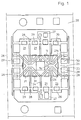
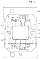
- FIG. 1 relates to the first embodiment and shows a greatly enlarged portion of a system carrier 20 in the form of a flat, normally punched sheet metal structure, which is usually also referred to as a 'lead frame'. As indicated by dash-dotted lines, further similar sections adjoin the side, that is to say that a longer, punched metal strip with a plurality of sections according to FIG. 1 is used in a known manner.
- a system carrier 20 In the center of the system carrier 20 there is a square, preferably rectangular or square chip island 22 . This is limited by slot-like openings 23 and held on both sides by bridges 25 .
- the slot-like openings 23 communicate with other slot-like openings 24 , and the latter, together with further openings, delimit approximately rectangular regions of the system carrier 20 , which are intended to form external contacts 21 on the finished electronic module.
- the present example is an electronic module for a semiconductor chip card in the manner of a credit card, which is why eight external contacts 21 , namely four each in two parallel rows and at predetermined locations within the chip card, are provided in accordance with the standard introduced for this purpose.
- the actual contact field 21a is bordered in dash-dotted lines in FIG. 1 on an external contact.
- the external contacts 21 as well as the bridges 25 have additional openings 31 in areas which are in the vicinity of the chip island 22 . Further outside, window-like openings 29 are provided in each external contact 21 and in the two bridges 25 . Approximately in line with these openings, the external contacts 21 and the bridges 25 are connected to one another by webs 28 , at which the slot-like openings 24 end.
- a semiconductor chip with an integrated circuit Arranged above the chip island 22 is a semiconductor chip with an integrated circuit, from which suitable areas are electrically connected to the external contacts 21 by means of electrically conductive wire connections.
- the dimensions of the semiconductor chip are not limited to the dimensions of the chip island 22 .
- two semiconductor chips 1a , 1b are shown in dash-dot lines, of which in reality only one semiconductor chip 1a or 1b is mounted.
- the small, square semiconductor chip 1a is located entirely on the chip island 22 .
- the semiconductor chip 1b which is rectangular and is substantially larger than the semiconductor chip 1a , projects beyond the chip island 22 on all sides and partially overlaps with the adjacent external contacts 21 ; the dimensions of the semiconductor chip 1b shown correspond to the maximum possible dimensions of the semiconductor chip in the present example.
- the slot-like openings 23 each of which is delimited on both sides in its longitudinal direction by a straight line, and which in turn border the chip island 22 and separate it from the external contacts 21 , to the edges of the square or rectangular semiconductor chip 1a , 1b run at an oblique angle, at a predeterminable angle, preferably as shown at an angle of approximately 45 °, so that the semiconductor chip 1 is arranged in a corner relative to the chip island 22 .
- the slot-like openings 24 separating the external contacts 21 and communicating with the slot-like openings 23 run along kinked lines, as a result of which these slot-like openings 24 also at least partially, mainly within the boundaries of the semiconductor chip 1b , also belong to the ones Edges of the semiconductor chip 1b are at an oblique angle.
- the slot-like openings 23, 24 mentioned form inevitable lines of weakness.
- the aforementioned measures or the overlapping of the semiconductor chip 1 relative to the chip island 22 ensure that the weakening lines of the system carrier 20 do not run parallel to the potential break lines of the semiconductor chip 1 , as a result of which the risk of breakage for the semiconductor chip 1 in the mechanical connection of the electronic module is considerably reduced .
- the arrangement is such that the diagonals of the square chip island 22 are parallel or perpendicular to the two rows of the external contacts 21 ; the chip island 22 could, for the same direction of the diagonals, also be approximately rhombic.
- a reverse arrangement is basically, for example, in another arrangement, the external contacts, conceivable in which respect, a square or rectangular chip island would arranged axially parallel to the leadframe 20, the semiconductor chip, however, an oblique angle to the system carrier 20 to the principal axes of the system carrier twentieth
- the course of the slot-like openings 24 separating the external contacts can also be varied, the desired effect being achieved to different degrees by the sections of these openings 24 that are inclined to the semiconductor chip 1b , especially in the areas covered by the semiconductor chip 1b .
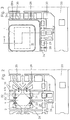
- the rectangular semiconductor chip 1 is mounted on the chip island 22 of the system carrier 20 .
- This semiconductor chip 1 is somewhat smaller than the maximum semiconductor chip 1b that can still be mounted according to FIG. 1 , but the semiconductor chip 1 projects significantly beyond the chip island 22 and overlaps with adjacent areas of the external contacts 21 .
- Wire connections 3 have already been produced in a known manner from corresponding regions of the circuit of the semiconductor chip 1 to the individual external contacts 21 .
- an insulating, at least on its side facing the lead frame 20 facing surface adhesive sheet 2 is mounted on the leadframe 20th
- This has about the format of the semiconductor chip 1 and consists of a temperature-resistant plastic, for example polyamide or polyester with an adhesive coating, which polymerizes at elevated temperature.
- a film 2 has the advantage of compensating for significant material-related differences in the heat dilatation between the metallic system carrier 20 and the semiconductor chip 1 and also of damping impacts which act on the system carrier 20 from the outside with respect to the semiconductor chip 1 .
- the semiconductor chip 1 is electrically insulated from the external contacts 21 by the film 2 .
- the assembly of the semiconductor chip 1 and the production of the wire connections 3 according to FIG. 2 take place fully automatically on powerful assembly devices, as are proven and widespread for the assembly of semiconductor chips on system carriers.
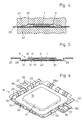
- the system carrier 20 equipped with the semiconductor chip 1 is introduced into an injection mold for the purpose of producing a flat plastic housing 10 , as is shown schematically in FIG. 4 ; it is preferably a multiple form in which the plastic housing of a plurality of electronic modules can be produced simultaneously.
- the essentially flat mold half 40 which is located at the bottom in FIGS . 4 to 6 , the also flat system carrier 20 lies on the entire surface, while the upper mold half 41 forms the mold cavity 10 ' .
- the semiconductor chip 1 and the system carrier 20 are encapsulated or molded with plastic compound by injection molding, as a result of which the outer contour of the plastic housing 10 is formed.
- the molded intermediate product with the plastic housing 10 is shown in FIG. 3 .
- all the slot-like openings 23 and 24 up to the webs 28 and also all other openings as shown in FIG. 1 have been filled with the plastic, with the exception, of course, of the openings and opening areas covered by the film 2 .
- the plastic mass, with the outside of the system carrier 20 resting on the lower mold half 40 is flush everywhere according to FIG. 4 ; this applies in particular to the cross section of all the openings 31 . 4 and 5 , the outer surface of the plastic housing 10 thus contains surface parts which are formed by the system carrier 20 , in particular also the external contacts 22 , and surface parts which are formed by the plastic mass, which are not caused by the Slide 2 covered breakthroughs has penetrated.
- the plastic material for the plastic housing 10 or a thermoset resin is used with a low viscosity to the wire connections during the casting process not to jeopardize by the inflowing pressurized plastic.
- the film 2 effectively prevents the plastic from reaching the underside of the external contacts 22 despite its low viscosity.
- a plastic with the lowest possible coefficient of thermal expansion is used, as is known for the encapsulation of silicon semiconductor chips under the name 'low stress' mass with a high quartz content.
- the metal of the system carrier 20 has a high coefficient of thermal expansion and expands accordingly in the mold 40, 41 at the processing temperature of the plastic to be pressed in.
- the relatively flat plastic housing 10 can be graduated in thickness, for example as shown in FIGS. 4 to 6 .
- the full housing thickness is only present in a central area where the plastic encloses the semiconductor chip 1 and forms the upper flat side 11 of the plastic housing 10 opposite the external contacts 22 or the lower flat side 12 .
- the intermediate product according to FIG. 3 formed after pressing the plastic housing 10 is now processed further.
- the electronic module is cut out of the frame of the system carrier 20 along two symmetrical lines 32 , of which only one is visible in FIG. 3 .
- the electrical functions of the electronic module can be tested via its external contacts 22 .
- extensions 26 and 27 or edge regions of the system carrier 20 around the housing 10 are bent along the bending lines 30 , such as 5 and 6 emerges. These offsets upwards and outwards take place in the direction of the outer surface 11 of the electronic module opposite the system carrier 20 ; in the present example, they extend over the entire thickness of the electronic module, such that the ends of the extensions 26 and 27 mentioned come to lie in the plane of the flat side 11 of the plastic housing 10 opposite the external contacts 21 .
- the two extensions 27 which are opposite each other with respect to the housing 10 , and a part of the extensions 26 are each mechanically connected to the external contacts 21 , while further extensions 26 originate from the two bridges 25 connected to the chip island 22 , as shown in FIG. 1 .
- the window-like openings 29 mentioned above in connection with FIG. 1 are now in the region of the offsets according to FIGS. 5 and 6 .
- Openings 35 are expediently provided in the ends of the two extensions 27 , for the grippers of an assembly robot to engage.
- centering openings 36 into which centering pins 46 of the casting mold according to FIG. 7 engage, in order to precisely position the electronics module in the mold cavity K ' for the chip card. It should be emphasized that this positioning takes place directly on the external contacts 22 of the electronic module and not indirectly via the plastic housing 10 of the electronic module; this results in a precise positioning of the external contacts 22 within the chip card.
- the extensions 27 of the system carrier 20 lying outside the plastic housing 10 are generally intended for interaction with automatic assembly machines when handling the electronics module designated M in FIG. 7 .
- the gripper and / or positioning contours 35, 36 which can also be designed differently than shown, are in exact positional relationship with the external contacts 21 of the electronic module M. This ensures safe, automatic manipulation and precise positioning, for example during test operations and when packing.
- a high positioning accuracy is obtained on the one hand by the attack on the system carrier 20 instead of the plastic housing, both due to the material and by the direct attack on the system carrier forming the external contacts, and on the other hand by the relatively large distance between the contours 36, 37 on the two extensions 27 .
- a thin decorative sheet be inserted 48th to which the electronic module M including 22 comes to lie with its flat side 12 of its external contacts.
- This decorative film 48 is, for example, a printed film for a thermal transfer printing process, in which the print pattern present on the film only connects to the plastic to be injected into the mold cavity K ' , but not to the metallic parts of the electronic module M.
- the relevant side of the chip card is printed with the decorative film 48 in a manner known per se.
- the electronics module M is covered in the upper mold half 45 by a label 47 which extends over the entire chip card and which in turn is printed.
- the plastic forming the chip card a thermoplastic, preferably ABS, is injected into the mold cavity K ' using known technology.
- the electronic module M is cast around it, being arranged flush with the plastic forming the chip card or in an aligned configuration.
- the thermoplastic plastic passes through the window-like openings 29 and laterally between all the extensions 26, 27 . This results in an extremely stable mechanical anchoring of the edge regions of the system carrier 20 which protrude beyond the plastic housing of the electronic module M in the plastic of the chip card. It is also important that the electronic module M on any of the flat sides 11, 12 of its plastic casing 10 with the thermoplastic plastic material of the chip card is back-cast. The thickness of the chip card is therefore equal to the thickness of the electronic module M.
- the entire possible thickness is therefore available for the plastic housing 10 of the electronics module M.
- a thickness of 0.72 mm thus remains for the plastic housing 10 of the electronic module M.
- the electronic module described or suitable variants of the same are recommended also for pouring into other flat chip cards or carrier bodies such as electronic Key.
- other types of installation and use are also possible, where the flat design of the electronic module is required or brings special advantages, such as for example for components for surface mounting (SMD technology, surface mounted devices).
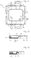
- FIGS. 8 to 13 A further embodiment of the electronic module in a flat design and the manufacture thereof can be seen from FIGS. 8 to 13 ; however, the injection molding of the plastic housing of the electronic module and the pouring of the electronic module into a chip card or another support body are not shown separately and reference is made to the relevant FIGS. 4 and 7 and the associated description.
- Some components of the electronic module according to the variant according to FIGS. 8 to 13 correspond to those of the embodiment described above and are provided with the same reference numerals.
- the following deviations from the system carrier 20 are to be mentioned on the system carrier 20 ' according to FIG. 8 : on the external contacts 21 , the parts removed from the chip island 22 are not connected to one another via webs corresponding to the webs 28 of FIG. 1 , but go separately the lateral edge areas of the system carrier 20 ' .
- the external contacts 21 have no openings corresponding to the openings 31 and 29 in FIG. 1 .
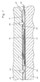
- the outer parts are connected to the system carrier 20 ′ via webs 16 , and slot-like openings 17 are provided on both sides of the webs 16 , which run parallel to each other and to the external contacts 21 and to the further bending lines 30 10, which can be seen from FIG . 9 shows the semiconductor chip 1 which is mounted on the system carrier 20 ' and is electrically connected to the external contacts 21 via the lines 3 .
- the semiconductor chip 1 is in turn connected to the system carrier 20 ' via the insulating film 2 ' lying between the semiconductor chip 1 and the system carrier 20 ' , but in the present embodiment the film 2' is extended far beyond the format of the semiconductor chip 1 by also expanding extends over the external contacts 21 and the bridges 25 and the slots 17 ; in particular, the film 2 ' also covers all of the slots 23 and 24 which delimit the chip island 22 and the external contacts 21 .
- the film 2 ' is e.g. B. made of ribbon material, typically made of polyimide, for example "KAPTON” or "MYLAR", of about 50 microns thick.
- the film 2 ' is perforated and has the following punched openings which are produced before being applied to the system carrier 20' : firstly two openings 5 which leave the webs 16 free, secondly openings 6 for the passage of the wires 3 onto the external contacts 21 , thirdly, an opening or bore 7 arranged for centering purposes, which is made to coincide with a corresponding bore 7 ' , shown in FIG. 8 , fourthly, an opening in the form of an edge cutout 8 in the region of a sprue 42 , which is used during the injection molding of the plastic housing 10 of the electronic module M is formed, the gate 42 and the plastic housing 10 in Fig. 9 shown in phantom, and sixthly, if necessary, an opening 9 in the area of the chip island 22 to the underside of the semiconductor chip 1 by means of a conductive adhesive to the lead frame 20 to connect.
- the prepared section of the film 2 ' can be laminated onto the system carrier 20' , as described above for the adhesive film 2 in connection with FIG. 2 .
- the assembly of the semiconductor chip 1 on the film 2 ' and the contacting by means of the wire connections 3 then also take place as described with reference to the embodiment of FIGS. 1 to 7 .
- the film 2 ' fulfills the task of producing an' elastic 'mechanical connection between the semiconductor chip 1 and the system carrier 20 , as well as further tasks: the adhesive film creates a large-area, intimate connection between the contacts 21 , the chip island 22 and the bridges 25 .
- the film 2 ' prevents the penetration of plastic into the slots 23, 24 and under the external contacts 21 on the lower outer surface of the electronic module M , ie the formation of annoying "flash" on this outside is prevented.
- the inherently insulating or high-resistance material from which the film 2 'is made and / or the adhesive layer can also have a certain targeted, low electrical conductivity, as a result of which voltage peaks, for example as a result of electrostatic discharges which reach the external contacts, are effectively damped so that you get a so-called 'ESD protection'; With chip cards, this is particularly important because the external contacts 22 are exposed there and are insulated from one another. An additional, important function of the film 2 ' in the area of the slots 17 is explained below with reference to FIGS. 11 and 13 .
- the mechanical connection of the plastic housing 10 to the system carrier 20 ' takes place practically exclusively indirectly via the film 2' .
- the adhesion of the plastic of the plastic housing 10 on the film 2 ' on the one hand and the adhesion of the film 2' on the system carrier 20 on the other hand is considerably stronger than the direct adhesion between the plastic of the plastic housing 10 and the metal of the system carrier 20 .
- the film 2 ' thus makes the electronics module M considerably more robust, and above all it effectively prevents the external contacts 21 from being detached or torn from the surface of the chip card.
- the sprue 42 which is located directly on the sheet metal of the system carrier 20 , can be easily detached from the latter and broken off at the edge of the plastic housing 10 .
- the edge regions of the metallic system carrier 20 lying on the edge of the electronic module are cranked along the bending lines 30 in a bending tool; however, the webs 16 remain flat and still hold the electronics module in association with the system carrier (s) 20 ' . Finally, the webs 16 are also cut away in a further punching tool and the finished electronic modules M are thus detached from the system carrier 20 ' , as can be seen from FIG. 11 .
- the electronics modules M according to FIGS. 11 to 13 which are produced fully automatically in the manner described, can now, analogously to the example described above with reference to FIG. 7 , be injection molded into a chip card or another carrier. This results in essentially the same properties and advantages with regard to reliable anchoring, etc.
- the encapsulation and connection with the plastic of the carrier surrounding the electronics module in turn takes place on the flat surface surrounding the plastic housing 10 , covered by the film 2 ′ , and on the bent parts 26 ', 27 and 34 , as can be easily seen from FIGS. 11 to 13 .
Description
- ein Elektronikmodul zu schaffen, welches sowohl bezüglich seiner Herstellung wie bezüglich seines Gebrauches optimal ausgebildet ist,
- ein Verfahren zur Herstellung des erfindungsgemässen Elektronikmoduls aufzuzeigen,
- eine Verwendung des erfindungsgemässen Elektronikmoduls zu zeigen und
- eine Chipkarte mit dem erfindungsgemässen Elektronikmodul vorzuschlagen.
- Fig. 1
- einen Systemträger für eine erste Ausführungsform eines Elektronikmoduls nach der Erfindung, von oben;
- Fig. 2 - 3
- aufeinanderfolgende Stufen während der Herstellung des auf dem Systemträger gemäss Fig. 1 aufgebauten Elektronikmoduls, von oben;
- Fig. 4
- den in Fig. 1 dargestellten Systemträger mit einem Halbleiterchip in einer Spritzgiessform, in welcher das in Fig. 2 gezeigte Zwischenprodukt hergestellt wird, in einem Schnitt entlang der Linie IV - IV der Fig. 2;
- Fig. 5
- das fertige, vom Systemträger freigeschnittene und verformte Elektronikmodul, in einem Schnitt entlang der Linie V - V der Fig. 3;
- Fig. 6
- das in Fig. 6 dargestellte Elektronikmodul, in einem Schaubild;
- Fig. 7
- das in den Fig. 6 und 7 dargestellte Elektronikmodul, eingelegt und positioniert in einer weiteren Spritzgiessform, in welcher das Elektronikmodul zur Herstellung einer Chipkarte umgossen wird, in vergrössertem Massstab, in einem Schnitt;
- Fig. 8
- einen Systemträger für eine zweite Ausführungsform des Elektronikmoduls, in gleicher Darstellung wie Fig. 1;
- Fig. 9 - 10
- aufeinanderfolgende Herstellungsstufen des auf dem Systemträger der Fig. 8 aufgebauten Elektronikmoduls, in den Fig. 2 und 3 entsprechenden Darstellungen;
- Fig. 11
- das in den Fig. 9 und 10 dargestellte Elektronikmodul, von oben;
- Fig. 12
- das in den Fig. 9 - 11 dargestellte Elektronikmodul, ausschnittweise in vergrössertem Massstab, in einem Schnitt längs der Linie C - C der Fig. 11, und
- Fig. 13
- das in Fig. 11 dargestellte Elektronikmodul, ausschnittweise in vergrössertem Massstab, in einem Schnitt längs der Linie D - D der Fig. 11.
Claims (11)
- Elektronikmodul (M) in Flachbauweise, umfassendeinen Systemträger (20, 20'), der aus einem Abschnitt eines Metallstreifens mit vorgestanzten Durchbrüchen gebildet und innerhalb von Randbereichen eben ist,von denen einige Durchbrüche (23, 24) schlitzartig und in ihrer Längsrichtung beidseitig geradlinig berandet sind und Aussenkontakte (21) sowie eine mindestens annähernd rechteckige, zur Aufnahme eines Halbleiterchips (1) bestimmte Chipinsel (22) begrenzen, undvon denen andere Durchbrüche (35, 36) in Randbereichen des Systemträgers (20, 20') angeordnet sind,den über der Chipinsel (20, 20') montierten rechteckigen Halbleiterchip (1), dessen Kanten gegenüber den Rändern der Chipinsel (20, 20') um einen Winkel gedreht sind, damit die durch die Durchbrüche (23, 24) verursachten Schwächungslinien des Systemträgers (20, 20') nicht mit den parallel zu den Kanten des Halbleiterchips (1) gerichteten potentiellen Bruchstellen des Halbleiterchips (1) zusammenfallen,Drahtverbindungen (3) zwischen dem Halbleiterchip (1) und den Aussenkontakten (21), undeine Kunststoffmasse, welche ein Kunststoffgehäuse (10) bildet und mit Ausnahme der Randbereiche des Systemträgers (20, 20') diesen überdeckt und den Halbleiterchip (1) und die Drahtverbindungen (3) umgibt, wobei die Aussenkontakte (21) an einer Flachseite des Kunststoffgehäuses (10) freiliegen.
- Elektronikmodul (M) nach Patentanspruch 1,
dadurch gekennzeichnet,
dass auf dem Systemträger (20, 20') eine Folie (2, 2') angebracht ist, wobei der Halbleiterchip (1) auf der Folie, (2, 2') oder in einer Aussparung der Folie (2, 2') montiert ist. - Elektronikmodul (M) nach mindestens einem der obigen Patentansprüche,
dadurch gekennzeichnet,
dass sich der Halbleiterchip (1a) vollständig über der Chipinsel (22) befindet. - Elektronikmodul (M) nach mindestens einem der obigen Patentansprüche,
dadurch gekennzeichnet,
dass der Halbleiterchip (1b) über die Chipinsel (22) hinausragt und sich mit mindestens einem Teil der Aussenkontakte (21) überlappt. - Elektronikmodul (M) nach mindestens einem der obigen Patentansprüche,
dadurch gekennzeichnet,
dass die Folie (2, 2') sich höchstens bis zu den die Chipinsel (22) begrenzenden Durchbrüchen (23) erstreckt. - Elektronikmodul (M) nach mindestens einem der obigen Patentansprüche,
dadurch gekennzeichnet,
dass sich die Folie (2, 2') höchstens innerhalb der Randbereiche erstreckt. - Verfahren zur Herstellung eines Elektronikmoduls (M) nach mindestens einem der obigen Patentansprüche, wobeiein als Systemträger (20, 20') dienender Abschnitt von einem ebenen Metallstreifen abgetrennt wird, welcher Systemträger (20) der Fläche des Elektronikmoduls (M) einschliesslich von Randbereichen entspricht, wobei im Metallstreifen Durchbrüche sind,von welchen einige Durchbrüche (23, 24) schlitzförmig sind und Aussenkontakte (21) sowie eine mindestens annähernde rechteckige, zur Aufnahme eines Halbleiterchips (1) bestimmte Chipinsel (22) begrenzen, wobei die schlitzförmigen Durchbrüche (23, 24) längs der Aussenkontakte b bzw. der Chipinsel (22) in ihrer Längsrichtung beidseitig durch Geraden berandet sind, undvon welchen andere Durchbrüche in den Randbereichen des Systemträgers (20. 20') angeordnet sind,über der Chipinsel (22) der viereckige Halbleiterchip (1) montiert wird, wobei seine Kanten gegenüber den die Chipinsel (22) begrenzenden Durchbrüchen (23) um einen vorgestimmten Winkel gedreht sind, damit die durch die Durchbrüche (23, 24) verursachten Schwächungslinien des Systemträgers (20, 20') nicht mit den parallel zu den Kanten des Halbleiterchips (1) gerichteten potentiellen Bruchstellen des Halbleiterchips (1) zusammenfallen,je eine Drahtverbindung (3) zwischen dem Halbleiterchip (1) und jedem der Aussenkontakte (21) hergestellt werden,der Systemträger (20, 20') mit dem Halbleiterchip (1) und den Drahtverbindungen (3) in eine einen Formhohlraum (10') bildende Giessform (40, 41) eingebracht wird, in welcher er aufliegt, wobei die Randbereiche des Systemträgers (20, 20') aus dem Formhohlraum (10') ragen,Kunststoff in den Formhohlraum (10') der Giessform (40, 41) eingebracht wird, um den Systemträger (20, 20') zu bedecken, den Halbleiterchip (1) mit den Drahtverbindungen (3) von oben und von den Seiten zu umpressen, zwecks Bildung eines Kunststoffgehäuses (10), an dessen unterer Flachseite (12) die Aussenkontakte (21) freiliegen, undder Systemträger (20, 20') ausserhalb der Randbereiche durchtrennt und die Randbereiche des Systemträgers (20, 20') an mindestens zwei sich gegenüberliegenden Seiten des Kunststoffgehäuses (20, 20') nach oben über die Höhe des Kunststoffgehäuses (10) und aussen abgekröpft werden.
- Verfahren nach Patentanspruch 7,
dadurch gekennzeichnet,
dass auf dem Systemträger (20, 20') eine mindestens einseitig klebende Folie (2, 2') angebracht wird, und dass der Halbleiterchip (1) auf der als mechanisches Dämpfungsglied wirkenden und einen Unterschied der Wärmedilatation von Halbleiterchip (1) und Systemträger (20, 20') ausgleichenden Folie (2, 2') oder in einer Aussparung der Folie (2, 2') montiert wird. - Verwendung des Elektronikmoduls (M) nach mindestens einem der Patentansprüche 1 bis 6 zur Herstellung einer Chipkarte,
dadurch gekennzeichnet,dass das Elektronikmodul (M) in eine einen Formhohlraum (K') bildende Giessform (44, 45) eingebracht wird, dessen Höhe im wesentlichen der Höhe des Kunststoffgehäuses (10) des Elektronikmoduls (M) entspricht, unddass der Formhohlraum (K') mit Kunststoff ausgegossen wird, wonach das Elektronikmodul (M) seitlich von Kunststoff umgeben ist, während die Flachseiten (11, 12) seines Kunststoffgehäuses (10) in einer Ebene mit den beiden Aussenflächen der Chipkarte liegen,wobei die Positionierung des Elektronikmoduls (M) durch Positionierung der Durchbrüche (35, 36) seiner Randbereiche erfolgt. - Verwendung des Elektronikmoduls nach Patentanspruch 9,
dadurch gekennzeichnet,
dass vor dem Einbringen des Kunststoffes in mindestens eine der Hälften der Giessform (44, 45) eine Dekorationsfolie (48) oder Etikette (47) eingelegt wird. - Chipkarte mit einem Elektronikmodul (M) nach mindestens einem der Patentansprüche 1 bis 6,
dadurch gekennzeichnet,
dass sie als rechteckige Kreditkarte oder als elektronischer Schlüssel, vorzugsweise mit einer schlüsselähnlichen Kontur, ausgebildet ist.
Applications Claiming Priority (4)
| Application Number | Priority Date | Filing Date | Title |
|---|---|---|---|
| CH363392 | 1992-11-27 | ||
| CH363392A CH686325A5 (de) | 1992-11-27 | 1992-11-27 | Elektronikmodul und Chip-Karte. |
| CH3633/92 | 1992-11-27 | ||
| EP93118564A EP0599194A1 (de) | 1992-11-27 | 1993-11-18 | Elektronikmodul in Flachbauweise |
Related Parent Applications (1)
| Application Number | Title | Priority Date | Filing Date |
|---|---|---|---|
| EP93118564A Division EP0599194A1 (de) | 1992-11-27 | 1993-11-18 | Elektronikmodul in Flachbauweise |
Publications (3)
| Publication Number | Publication Date |
|---|---|
| EP0843358A2 EP0843358A2 (de) | 1998-05-20 |
| EP0843358A3 EP0843358A3 (de) | 1998-05-27 |
| EP0843358B1 true EP0843358B1 (de) | 2000-05-10 |
Family
ID=4260178
Family Applications (4)
| Application Number | Title | Priority Date | Filing Date |
|---|---|---|---|
| EP95118345A Withdrawn EP0706214A3 (de) | 1992-11-27 | 1993-11-18 | Elektronikmodul und Chipkarte |
| EP93118564A Withdrawn EP0599194A1 (de) | 1992-11-27 | 1993-11-18 | Elektronikmodul in Flachbauweise |
| EP98101884A Expired - Lifetime EP0843358B1 (de) | 1992-11-27 | 1993-11-18 | Elektronikmodul in Flachbauweise und Chipkarte |
| EP00106889A Withdrawn EP1028462A1 (de) | 1992-11-27 | 1993-11-18 | Elektronikmodul in Flachbauweise |
Family Applications Before (2)
| Application Number | Title | Priority Date | Filing Date |
|---|---|---|---|
| EP95118345A Withdrawn EP0706214A3 (de) | 1992-11-27 | 1993-11-18 | Elektronikmodul und Chipkarte |
| EP93118564A Withdrawn EP0599194A1 (de) | 1992-11-27 | 1993-11-18 | Elektronikmodul in Flachbauweise |
Family Applications After (1)
| Application Number | Title | Priority Date | Filing Date |
|---|---|---|---|
| EP00106889A Withdrawn EP1028462A1 (de) | 1992-11-27 | 1993-11-18 | Elektronikmodul in Flachbauweise |
Country Status (11)
| Country | Link |
|---|---|
| US (1) | US5550402A (de) |
| EP (4) | EP0706214A3 (de) |
| JP (1) | JP2515086B2 (de) |
| KR (1) | KR0174761B1 (de) |
| AT (1) | ATE192883T1 (de) |
| AU (2) | AU671868B2 (de) |
| CA (1) | CA2109761C (de) |
| CH (1) | CH686325A5 (de) |
| DE (1) | DE59310040D1 (de) |
| IL (1) | IL107696A (de) |
| MY (1) | MY111079A (de) |
Cited By (1)
| Publication number | Priority date | Publication date | Assignee | Title |
|---|---|---|---|---|
| CN103928431A (zh) * | 2012-10-31 | 2014-07-16 | 矽力杰半导体技术(杭州)有限公司 | 一种倒装封装装置 |
Families Citing this family (46)
| Publication number | Priority date | Publication date | Assignee | Title |
|---|---|---|---|---|
| JP3383398B2 (ja) * | 1994-03-22 | 2003-03-04 | 株式会社東芝 | 半導体パッケージ |
| DE4443767A1 (de) * | 1994-12-08 | 1996-06-13 | Giesecke & Devrient Gmbh | Elektronisches Modul und Datenträger mit elektrischem Modul |
| DE19512191C2 (de) * | 1995-03-31 | 2000-03-09 | Siemens Ag | Kartenförmiger Datenträger und Leadframe zur Verwendung in einem solchen Datenträger |
| KR0170316B1 (ko) * | 1995-07-13 | 1999-02-01 | 김광호 | 반도체 장치의 패드 설계 방법 |
| JPH0964240A (ja) | 1995-08-25 | 1997-03-07 | Toshiba Corp | 半導体装置および半導体装置の製造方法 |
| DE19607212C1 (de) * | 1996-02-26 | 1997-04-10 | Richard Herbst | Verbundkörper, Verfahren und Kunststoff-Spritzgießwerkzeug zur Herstellung eines solchen |
| CN1134064C (zh) * | 1996-05-17 | 2004-01-07 | 西门子公司 | 半导体芯片用的载体元件 |
| JPH09327990A (ja) * | 1996-06-11 | 1997-12-22 | Toshiba Corp | カード型記憶装置 |
| US5796586A (en) * | 1996-08-26 | 1998-08-18 | National Semiconductor, Inc. | Substrate board having an anti-adhesive solder mask |
| US5796570A (en) * | 1996-09-19 | 1998-08-18 | National Semiconductor Corporation | Electrostatic discharge protection package |
| US5773876A (en) * | 1996-11-06 | 1998-06-30 | National Semiconductor Corporation | Lead frame with electrostatic discharge protection |
| US5907769A (en) * | 1996-12-30 | 1999-05-25 | Micron Technology, Inc. | Leads under chip in conventional IC package |
| DE19721281C2 (de) * | 1997-05-21 | 1999-04-01 | Ods Landis & Gyr Gmbh & Co Kg | Chipmodul für eine Chipkarte |
| TW330337B (en) * | 1997-05-23 | 1998-04-21 | Siliconware Precision Industries Co Ltd | Semiconductor package with detached die pad |
| EP0938060A1 (de) * | 1998-02-20 | 1999-08-25 | ESEC Management SA | Verfahren zur Herstellung eines Chipobjektes und Chipobjekt |
| WO1999050792A1 (en) * | 1998-03-27 | 1999-10-07 | Koninklijke Philips Electronics N.V. | Data carrier having an implanted module based on a metal lead frame |
| EP1068640A1 (de) * | 1998-04-06 | 2001-01-17 | Infineon Technologies AG | Verwendung der baulichen beschaffenheit eines elektronischen bauteils als referenz bei der positionierung des bauteils |
| DE19816066A1 (de) * | 1998-04-09 | 1999-10-14 | Philips Patentverwaltung | Folie als Träger von integrierten Schaltungen |
| FR2781068B1 (fr) | 1998-07-07 | 2000-10-13 | Rue Cartes Et Systemes De | Procede de fabrication d'une carte a microcircuit permettant de limiter les contraintes mecaniques transmises a celui-ci et carte ainsi obtenue |
| EP1118111A1 (de) * | 1998-09-29 | 2001-07-25 | Tyco Electronics Logistics AG | Verfahren zum eingiessen eines flachen elektronikmoduls in einen kunststoffkartenkörper durch thermoplastisches spritzgiessen |
| EP1009023A1 (de) * | 1998-12-09 | 2000-06-14 | ESEC Management SA | Verfahren zur Verbindung von zwei Leiterstrukturen und Kunststoffobjekt |
| US6179210B1 (en) * | 1999-02-09 | 2001-01-30 | Motorola, Inc. | Punch out pattern for hot melt tape used in smartcards |
| DE19922473A1 (de) * | 1999-05-19 | 2000-11-30 | Giesecke & Devrient Gmbh | Chipträgermodul |
| JP3822768B2 (ja) * | 1999-12-03 | 2006-09-20 | 株式会社ルネサステクノロジ | Icカードの製造方法 |
| EP1119047A1 (de) * | 2000-01-18 | 2001-07-25 | Infineon Technologies AG | Flächiger Träger für ein Chipmodul und Herstellungsverfahren für ein Chipmodul |
| US6538304B1 (en) * | 2000-11-16 | 2003-03-25 | Texas Instruments Incorporated | Corner bonding to lead frame |
| DE10111028A1 (de) * | 2001-03-07 | 2002-09-19 | Infineon Technologies Ag | Chipkartenmodul |
| DE10158770B4 (de) * | 2001-11-29 | 2006-08-03 | Infineon Technologies Ag | Leiterrahmen und Bauelement mit einem Leiterrahmen |
| CA2524328C (en) * | 2003-05-09 | 2011-01-04 | Widex A/S | A method for manufacturing a carrier element for a hearing aid and a carrier element for a hearing aid |
| DE10333840B4 (de) * | 2003-07-24 | 2006-12-28 | Infineon Technologies Ag | Halbleiterbauteil mit einem Kunststoffgehäuse, das eine Umverdrahrungsstruktur aufweist und Verfahren zu deren Herstellung |
| DE202004003554U1 (de) | 2004-03-04 | 2004-06-03 | Novacard Informationssysteme Gmbh | Chipkarte |
| US7495926B2 (en) * | 2004-10-05 | 2009-02-24 | Sony Ericsson Mobile Communications Ab | Interface module for electronic devices |
| US7714415B2 (en) * | 2006-04-28 | 2010-05-11 | Intersil Americas, Inc. | Leadframe structures for semiconductor packages |
| DE102007038318A1 (de) * | 2007-08-14 | 2009-02-19 | Giesecke & Devrient Gmbh | Hochgeprägter kartenförmiger Datenträger |
| JP2009253153A (ja) * | 2008-04-09 | 2009-10-29 | Asmo Co Ltd | 樹脂封止型半導体装置 |
| JP5649277B2 (ja) | 2008-12-22 | 2015-01-07 | ローム株式会社 | 半導体装置 |
| CN102484083A (zh) * | 2009-09-11 | 2012-05-30 | 罗姆股份有限公司 | 半导体装置及其制造方法 |
| EP2369904A1 (de) * | 2010-03-16 | 2011-09-28 | Gemalto SA | Elektronisches Modul mit seitlichen Kontakten, Vorrichtung mit einem solchen Modul und Herstellungsverfahren eines solchen Moduls |
| US8649820B2 (en) | 2011-11-07 | 2014-02-11 | Blackberry Limited | Universal integrated circuit card apparatus and related methods |
| US8936199B2 (en) | 2012-04-13 | 2015-01-20 | Blackberry Limited | UICC apparatus and related methods |
| USD703208S1 (en) | 2012-04-13 | 2014-04-22 | Blackberry Limited | UICC apparatus |
| USD701864S1 (en) | 2012-04-23 | 2014-04-01 | Blackberry Limited | UICC apparatus |
| EP2731058A1 (de) * | 2012-11-13 | 2014-05-14 | Gemalto SA | Verfahren zur Herstellung eines elektronischen Chip-Moduls gegen elektrostatische Entladungen |
| US11416728B2 (en) | 2019-08-15 | 2022-08-16 | Federal Card Services, LLC | Durable dual interface metal transaction cards |
| US11455507B2 (en) | 2019-10-13 | 2022-09-27 | Federal Card Services, LLC | Metal transaction cards containing ceramic having selected coloring and texture |
| WO2022227537A1 (zh) * | 2021-04-29 | 2022-11-03 | 上海凯虹科技电子有限公司 | 半导体器件及引线框架 |
Family Cites Families (28)
| Publication number | Priority date | Publication date | Assignee | Title |
|---|---|---|---|---|
| GB1383297A (en) * | 1972-02-23 | 1974-02-12 | Plessey Co Ltd | Electrical integrated circuit package |
| US4215360A (en) * | 1978-11-09 | 1980-07-29 | General Motors Corporation | Power semiconductor device assembly having a lead frame with interlock members |
| DE3029667A1 (de) * | 1980-08-05 | 1982-03-11 | GAO Gesellschaft für Automation und Organisation mbH, 8000 München | Traegerelement fuer einen ic-baustein |
| DE3130213A1 (de) * | 1981-07-30 | 1983-02-17 | Siemens AG, 1000 Berlin und 8000 München | Verfahren zur herstellung einer tragbaren karte zur informationsverarbeitung |
| JPS60747A (ja) * | 1983-06-17 | 1985-01-05 | Hitachi Ltd | レジンモ−ルドicパツケ−ジ |
| JPS60171733A (ja) * | 1984-02-17 | 1985-09-05 | Hitachi Micro Comput Eng Ltd | 半導体装置 |
| JPS615530A (ja) * | 1984-06-20 | 1986-01-11 | Hitachi Ltd | 半導体装置 |
| FR2579798B1 (fr) * | 1985-04-02 | 1990-09-28 | Ebauchesfabrik Eta Ag | Procede de fabrication de modules electroniques pour cartes a microcircuits et modules obtenus selon ce procede |
| JPS61234129A (ja) * | 1985-04-09 | 1986-10-18 | Yaesu Musen Co Ltd | トランシ−バの制御方式 |
| JPS61269345A (ja) * | 1985-05-24 | 1986-11-28 | Hitachi Ltd | 半導体装置 |
| FR2584862B1 (fr) * | 1985-07-12 | 1988-05-20 | Eurotechnique Sa | Procede de fabrication en continu de micromodules pour cartes contenant des composants, bande continue de micromodules et micromodules realises selon un tel procede |
| JP2505172B2 (ja) * | 1986-09-30 | 1996-06-05 | 日立マクセル株式会社 | Icカ−ド |
| CA1290676C (en) * | 1987-03-30 | 1991-10-15 | William Frank Graham | Method for bonding integrated circuit chips |
| US5150193A (en) * | 1987-05-27 | 1992-09-22 | Hitachi, Ltd. | Resin-encapsulated semiconductor device having a particular mounting structure |
| JP2696532B2 (ja) * | 1988-08-19 | 1998-01-14 | 株式会社日立製作所 | 半導体装置およびその製造方法 |
| DE3809005A1 (de) * | 1988-03-17 | 1989-09-28 | Hitachi Semiconductor Europ Gm | Chipmodul und seine herstellung und verwendung |
| US4937656A (en) * | 1988-04-22 | 1990-06-26 | Mitsubishi Denki Kabushiki Kaisha | Semiconductor device |
| JPH01270338A (ja) * | 1988-04-22 | 1989-10-27 | Mitsubishi Electric Corp | モールド封止半導体装置 |
| EP0339763A3 (de) * | 1988-04-28 | 1990-04-25 | Citizen Watch Co. Ltd. | IC-Karte |
| JPH02144658A (ja) * | 1988-11-28 | 1990-06-04 | Hitachi Ltd | 文字の配置制御方式 |
| FR2645680B1 (fr) * | 1989-04-07 | 1994-04-29 | Thomson Microelectronics Sa Sg | Encapsulation de modules electroniques et procede de fabrication |
| JPH0726139Y2 (ja) * | 1989-04-17 | 1995-06-14 | リズム時計工業株式会社 | Icカード |
| FR2659157B2 (fr) | 1989-05-26 | 1994-09-30 | Lemaire Gerard | Procede de fabrication d'une carte dite carte a puce, et carte obtenue par ce procede. |
| DE3924439A1 (de) * | 1989-07-24 | 1991-04-18 | Edgar Schneider | Traegerelement mit wenigstens einem integrierten schaltkreis, insbesondere zum einbau in chip-karten, sowie verfahren zur herstellung dieser traegerelemente |
| JPH0373560A (ja) * | 1989-08-14 | 1991-03-28 | Nec Corp | 半導体装置 |
| JPH0793400B2 (ja) * | 1990-03-06 | 1995-10-09 | 株式会社東芝 | 半導体装置 |
| FR2673042A1 (fr) * | 1991-02-18 | 1992-08-21 | Em Microelectronic Marin Sa | Module electronique resistant aux deformations mecaniques pour carte a microcircuits. |
| JP2927982B2 (ja) * | 1991-03-18 | 1999-07-28 | ジャパンゴアテックス株式会社 | 半導体装置 |
-
1992
- 1992-11-27 CH CH363392A patent/CH686325A5/de not_active IP Right Cessation
-
1993
- 1993-11-18 EP EP95118345A patent/EP0706214A3/de not_active Withdrawn
- 1993-11-18 EP EP93118564A patent/EP0599194A1/de not_active Withdrawn
- 1993-11-18 AT AT98101884T patent/ATE192883T1/de active
- 1993-11-18 DE DE59310040T patent/DE59310040D1/de not_active Expired - Fee Related
- 1993-11-18 EP EP98101884A patent/EP0843358B1/de not_active Expired - Lifetime
- 1993-11-18 EP EP00106889A patent/EP1028462A1/de not_active Withdrawn
- 1993-11-19 JP JP5290842A patent/JP2515086B2/ja not_active Expired - Lifetime
- 1993-11-22 IL IL107696A patent/IL107696A/en not_active IP Right Cessation
- 1993-11-22 AU AU51848/93A patent/AU671868B2/en not_active Ceased
- 1993-11-23 US US08/156,295 patent/US5550402A/en not_active Expired - Fee Related
- 1993-11-23 CA CA002109761A patent/CA2109761C/en not_active Expired - Fee Related
- 1993-11-26 MY MYPI93002490A patent/MY111079A/en unknown
- 1993-11-26 KR KR1019930025433A patent/KR0174761B1/ko not_active IP Right Cessation
-
1996
- 1996-07-04 AU AU58375/96A patent/AU688682B2/en not_active Ceased
Cited By (2)
| Publication number | Priority date | Publication date | Assignee | Title |
|---|---|---|---|---|
| CN103928431A (zh) * | 2012-10-31 | 2014-07-16 | 矽力杰半导体技术(杭州)有限公司 | 一种倒装封装装置 |
| CN103928431B (zh) * | 2012-10-31 | 2017-03-01 | 矽力杰半导体技术(杭州)有限公司 | 一种倒装封装装置 |
Also Published As
| Publication number | Publication date |
|---|---|
| KR0174761B1 (ko) | 1999-02-01 |
| EP0843358A3 (de) | 1998-05-27 |
| DE59310040D1 (de) | 2000-06-15 |
| AU688682B2 (en) | 1998-03-12 |
| IL107696A (en) | 1998-02-22 |
| CA2109761C (en) | 1998-01-06 |
| EP0599194A1 (de) | 1994-06-01 |
| EP1028462A1 (de) | 2000-08-16 |
| CA2109761A1 (en) | 1994-05-28 |
| AU5837596A (en) | 1996-09-05 |
| KR940013306A (ko) | 1994-06-25 |
| CH686325A5 (de) | 1996-02-29 |
| AU5184893A (en) | 1994-06-09 |
| JP2515086B2 (ja) | 1996-07-10 |
| MY111079A (en) | 1999-08-30 |
| IL107696A0 (en) | 1994-02-27 |
| EP0706214A3 (de) | 1998-01-14 |
| ATE192883T1 (de) | 2000-05-15 |
| EP0706214A2 (de) | 1996-04-10 |
| AU671868B2 (en) | 1996-09-12 |
| US5550402A (en) | 1996-08-27 |
| JPH06236958A (ja) | 1994-08-23 |
| EP0843358A2 (de) | 1998-05-20 |
Similar Documents
| Publication | Publication Date | Title |
|---|---|---|
| EP0843358B1 (de) | Elektronikmodul in Flachbauweise und Chipkarte | |
| DE3153769C2 (de) | Trägerelement zum Einbau in Ausweiskarten | |
| EP0756244B1 (de) | Schaltungseinheit und Verfahren zur Herstellung einer Schaltungseinheit | |
| DE69735361T2 (de) | Harzverkapselte halbleiteranordnung und herstellungsverfahren dafür | |
| DE2942397A1 (de) | Traegerband fuer elektronische schaltkreiselemente, verfahren zu seiner herstellung und anwendung bei einer signalverarbeitungseinrichtung | |
| EP0710919A2 (de) | Kontaktloses elektronisches Modul | |
| DE69534483T2 (de) | Leiterrahmen und Halbleiterbauelement | |
| DE3623419C2 (de) | ||
| DE4443767A1 (de) | Elektronisches Modul und Datenträger mit elektrischem Modul | |
| DE10223035A1 (de) | Elektronisches Bauteil mit Hohlraumgehäuse, insbesondere Hochfrequenz-Leistungsmodul | |
| DE10145752B4 (de) | Nicht-leitendes, ein Band oder einen Nutzen bildendes Substrat, auf dem eine Vielzahl von Trägerelementen ausgebildet ist | |
| DE10232788B4 (de) | Elektronisches Bauteil mit einem Halbleiterchip auf einem Systemträger, Systemträger und Verfahren zur Herstellung eines elektronischen Bauteils | |
| DE2855838C2 (de) | Bauteilanordnung | |
| DE19532755C1 (de) | Chipmodul, insbesondere für den Einbau in Chipkarten, und Verfahren zur Herstellung eines derartigen Chipmoduls | |
| DE19543427A1 (de) | Chipmodul | |
| DE2306288A1 (de) | Traeger fuer integrierte schaltungen | |
| DE602004004647T2 (de) | Verfahren zum zusammenbauen eines elektronischen komponent auf einem substrat | |
| DE19614501C2 (de) | Verfahren zum Herstellen eines Keramik-Metall-Substrates sowie Keramik-Metall-Substrat | |
| DE102005007643A1 (de) | Verfahren und Anordnung zum Kontaktieren von Halbleiterchips auf einem metallischen Substrat | |
| EP2260511B1 (de) | Bauelementanordnung und verfahren zur herstellung einer bauelementanordnung | |
| DE19809073A1 (de) | Chipmodul und Verfahren zur Herstellung einer Chipkarte | |
| DE102014108916B4 (de) | Bandförmiges Substrat zur Herstellung von Chipträgern, elektronisches Modul mit einem solchen Chipträger, elektronische Einrichtung mit einem solchen Modul und Verfahren zur Herstellung eines Substrates | |
| DE2929339A1 (de) | Halbleiteranordnung | |
| DE4041346B4 (de) | Standard-Kunststoffgehäuse mit darin verkapselten Halbleiterchips | |
| DE10358423B4 (de) | Modulbrücken für Smart Labels |
Legal Events
| Date | Code | Title | Description |
|---|---|---|---|
| PUAI | Public reference made under article 153(3) epc to a published international application that has entered the european phase |
Free format text: ORIGINAL CODE: 0009012 |
|
| PUAL | Search report despatched |
Free format text: ORIGINAL CODE: 0009013 |
|
| AC | Divisional application: reference to earlier application |
Ref document number: 599194 Country of ref document: EP |
|
| AK | Designated contracting states |
Kind code of ref document: A2 Designated state(s): AT BE CH DE DK ES FR GB GR IE IT LI LU MC NL PT SE |
|
| AK | Designated contracting states |
Kind code of ref document: A3 Designated state(s): AT BE CH DE DK ES FR GB GR IE IT LI LU MC NL PT SE |
|
| RHK1 | Main classification (correction) |
Ipc: H01L 23/495 |
|
| 17P | Request for examination filed |
Effective date: 19980723 |
|
| RAP1 | Party data changed (applicant data changed or rights of an application transferred) |
Owner name: ESEC SEMPAC S.A. |
|
| GRAG | Despatch of communication of intention to grant |
Free format text: ORIGINAL CODE: EPIDOS AGRA |
|
| 17Q | First examination report despatched |
Effective date: 19990115 |
|
| GRAG | Despatch of communication of intention to grant |
Free format text: ORIGINAL CODE: EPIDOS AGRA |
|
| GRAG | Despatch of communication of intention to grant |
Free format text: ORIGINAL CODE: EPIDOS AGRA |
|
| GRAH | Despatch of communication of intention to grant a patent |
Free format text: ORIGINAL CODE: EPIDOS IGRA |
|
| GRAH | Despatch of communication of intention to grant a patent |
Free format text: ORIGINAL CODE: EPIDOS IGRA |
|
| GRAA | (expected) grant |
Free format text: ORIGINAL CODE: 0009210 |
|
| RAP1 | Party data changed (applicant data changed or rights of an application transferred) |
Owner name: SEMPAC SA |
|
| AC | Divisional application: reference to earlier application |
Ref document number: 599194 Country of ref document: EP |
|
| AK | Designated contracting states |
Kind code of ref document: B1 Designated state(s): AT BE CH DE DK ES FR GB GR IE IT LI LU MC NL PT SE |
|
| PG25 | Lapsed in a contracting state [announced via postgrant information from national office to epo] |
Ref country code: NL Free format text: LAPSE BECAUSE OF FAILURE TO SUBMIT A TRANSLATION OF THE DESCRIPTION OR TO PAY THE FEE WITHIN THE PRESCRIBED TIME-LIMIT Effective date: 20000510 Ref country code: GR Free format text: LAPSE BECAUSE OF NON-PAYMENT OF DUE FEES Effective date: 20000510 Ref country code: ES Free format text: THE PATENT HAS BEEN ANNULLED BY A DECISION OF A NATIONAL AUTHORITY Effective date: 20000510 |
|
| REF | Corresponds to: |
Ref document number: 192883 Country of ref document: AT Date of ref document: 20000515 Kind code of ref document: T |
|
| REG | Reference to a national code |
Ref country code: CH Ref legal event code: EP |
|
| REG | Reference to a national code |
Ref country code: IE Ref legal event code: FG4D Free format text: GERMAN |
|
| ITF | It: translation for a ep patent filed |
Owner name: KARAGHIOSOFF GIORGIO |
|
| REF | Corresponds to: |
Ref document number: 59310040 Country of ref document: DE Date of ref document: 20000615 |
|
| ET | Fr: translation filed | ||
| GBT | Gb: translation of ep patent filed (gb section 77(6)(a)/1977) |
Effective date: 20000714 |
|
| PG25 | Lapsed in a contracting state [announced via postgrant information from national office to epo] |
Ref country code: SE Free format text: LAPSE BECAUSE OF FAILURE TO SUBMIT A TRANSLATION OF THE DESCRIPTION OR TO PAY THE FEE WITHIN THE PRESCRIBED TIME-LIMIT Effective date: 20000810 Ref country code: PT Free format text: LAPSE BECAUSE OF FAILURE TO SUBMIT A TRANSLATION OF THE DESCRIPTION OR TO PAY THE FEE WITHIN THE PRESCRIBED TIME-LIMIT Effective date: 20000810 Ref country code: DK Free format text: LAPSE BECAUSE OF FAILURE TO SUBMIT A TRANSLATION OF THE DESCRIPTION OR TO PAY THE FEE WITHIN THE PRESCRIBED TIME-LIMIT Effective date: 20000810 |
|
| NLV1 | Nl: lapsed or annulled due to failure to fulfill the requirements of art. 29p and 29m of the patents act | ||
| PG25 | Lapsed in a contracting state [announced via postgrant information from national office to epo] |
Ref country code: LU Free format text: LAPSE BECAUSE OF NON-PAYMENT OF DUE FEES Effective date: 20001118 Ref country code: AT Free format text: LAPSE BECAUSE OF NON-PAYMENT OF DUE FEES Effective date: 20001118 |
|
| PG25 | Lapsed in a contracting state [announced via postgrant information from national office to epo] |
Ref country code: MC Free format text: LAPSE BECAUSE OF NON-PAYMENT OF DUE FEES Effective date: 20001130 Ref country code: LI Free format text: LAPSE BECAUSE OF NON-PAYMENT OF DUE FEES Effective date: 20001130 Ref country code: CH Free format text: LAPSE BECAUSE OF NON-PAYMENT OF DUE FEES Effective date: 20001130 Ref country code: BE Free format text: LAPSE BECAUSE OF NON-PAYMENT OF DUE FEES Effective date: 20001130 |
|
| PG25 | Lapsed in a contracting state [announced via postgrant information from national office to epo] |
Ref country code: IE Free format text: LAPSE BECAUSE OF NON-PAYMENT OF DUE FEES Effective date: 20010309 |
|
| PLBE | No opposition filed within time limit |
Free format text: ORIGINAL CODE: 0009261 |
|
| STAA | Information on the status of an ep patent application or granted ep patent |
Free format text: STATUS: NO OPPOSITION FILED WITHIN TIME LIMIT |
|
| REG | Reference to a national code |
Ref country code: IE Ref legal event code: FD4D |
|
| 26N | No opposition filed | ||
| BERE | Be: lapsed |
Owner name: S.A. SEMPAC Effective date: 20001130 |
|
| REG | Reference to a national code |
Ref country code: CH Ref legal event code: PL |
|
| REG | Reference to a national code |
Ref country code: GB Ref legal event code: IF02 |
|
| REG | Reference to a national code |
Ref country code: GB Ref legal event code: 732E |
|
| PGFP | Annual fee paid to national office [announced via postgrant information from national office to epo] |
Ref country code: GB Payment date: 20021021 Year of fee payment: 10 |
|
| PGFP | Annual fee paid to national office [announced via postgrant information from national office to epo] |
Ref country code: FR Payment date: 20021119 Year of fee payment: 10 |
|
| PGFP | Annual fee paid to national office [announced via postgrant information from national office to epo] |
Ref country code: DE Payment date: 20021128 Year of fee payment: 10 |
|
| REG | Reference to a national code |
Ref country code: FR Ref legal event code: TP |
|
| PG25 | Lapsed in a contracting state [announced via postgrant information from national office to epo] |
Ref country code: GB Free format text: LAPSE BECAUSE OF NON-PAYMENT OF DUE FEES Effective date: 20031118 |
|
| PG25 | Lapsed in a contracting state [announced via postgrant information from national office to epo] |
Ref country code: DE Free format text: LAPSE BECAUSE OF NON-PAYMENT OF DUE FEES Effective date: 20040602 |
|
| GBPC | Gb: european patent ceased through non-payment of renewal fee |
Effective date: 20031118 |
|
| PG25 | Lapsed in a contracting state [announced via postgrant information from national office to epo] |
Ref country code: FR Free format text: LAPSE BECAUSE OF NON-PAYMENT OF DUE FEES Effective date: 20040730 |
|
| REG | Reference to a national code |
Ref country code: FR Ref legal event code: ST |
|
| PG25 | Lapsed in a contracting state [announced via postgrant information from national office to epo] |
Ref country code: IT Free format text: LAPSE BECAUSE OF NON-PAYMENT OF DUE FEES;WARNING: LAPSES OF ITALIAN PATENTS WITH EFFECTIVE DATE BEFORE 2007 MAY HAVE OCCURRED AT ANY TIME BEFORE 2007. THE CORRECT EFFECTIVE DATE MAY BE DIFFERENT FROM THE ONE RECORDED. Effective date: 20051118 |